EP2597693A1 - Self-referenced MRAM cell with optimized reliability - Google Patents
Self-referenced MRAM cell with optimized reliability Download PDFInfo
- Publication number
- EP2597693A1 EP2597693A1 EP20120007861 EP12007861A EP2597693A1 EP 2597693 A1 EP2597693 A1 EP 2597693A1 EP 20120007861 EP20120007861 EP 20120007861 EP 12007861 A EP12007861 A EP 12007861A EP 2597693 A1 EP2597693 A1 EP 2597693A1
- Authority
- EP
- European Patent Office
- Prior art keywords
- storage
- magnetizations
- layer
- magnetic
- magnetization
- Prior art date
- Legal status (The legal status is an assumption and is not a legal conclusion. Google has not performed a legal analysis and makes no representation as to the accuracy of the status listed.)
- Granted
Links
Images
Classifications
-
- G—PHYSICS
- G11—INFORMATION STORAGE
- G11C—STATIC STORES
- G11C11/00—Digital stores characterised by the use of particular electric or magnetic storage elements; Storage elements therefor
- G11C11/02—Digital stores characterised by the use of particular electric or magnetic storage elements; Storage elements therefor using magnetic elements
- G11C11/16—Digital stores characterised by the use of particular electric or magnetic storage elements; Storage elements therefor using magnetic elements using elements in which the storage effect is based on magnetic spin effect
- G11C11/161—Digital stores characterised by the use of particular electric or magnetic storage elements; Storage elements therefor using magnetic elements using elements in which the storage effect is based on magnetic spin effect details concerning the memory cell structure, e.g. the layers of the ferromagnetic memory cell
-
- G—PHYSICS
- G11—INFORMATION STORAGE
- G11C—STATIC STORES
- G11C11/00—Digital stores characterised by the use of particular electric or magnetic storage elements; Storage elements therefor
- G11C11/02—Digital stores characterised by the use of particular electric or magnetic storage elements; Storage elements therefor using magnetic elements
- G11C11/16—Digital stores characterised by the use of particular electric or magnetic storage elements; Storage elements therefor using magnetic elements using elements in which the storage effect is based on magnetic spin effect
- G11C11/165—Auxiliary circuits
- G11C11/1673—Reading or sensing circuits or methods
-
- G—PHYSICS
- G11—INFORMATION STORAGE
- G11C—STATIC STORES
- G11C11/00—Digital stores characterised by the use of particular electric or magnetic storage elements; Storage elements therefor
- G11C11/02—Digital stores characterised by the use of particular electric or magnetic storage elements; Storage elements therefor using magnetic elements
- G11C11/16—Digital stores characterised by the use of particular electric or magnetic storage elements; Storage elements therefor using magnetic elements using elements in which the storage effect is based on magnetic spin effect
- G11C11/165—Auxiliary circuits
- G11C11/1675—Writing or programming circuits or methods
-
- H—ELECTRICITY
- H01—ELECTRIC ELEMENTS
- H01F—MAGNETS; INDUCTANCES; TRANSFORMERS; SELECTION OF MATERIALS FOR THEIR MAGNETIC PROPERTIES
- H01F10/00—Thin magnetic films, e.g. of one-domain structure
- H01F10/32—Spin-exchange-coupled multilayers, e.g. nanostructured superlattices
- H01F10/324—Exchange coupling of magnetic film pairs via a very thin non-magnetic spacer, e.g. by exchange with conduction electrons of the spacer
- H01F10/3263—Exchange coupling of magnetic film pairs via a very thin non-magnetic spacer, e.g. by exchange with conduction electrons of the spacer the exchange coupling being symmetric, e.g. for dual spin valve, e.g. NiO/Co/Cu/Co/Cu/Co/NiO
-
- H—ELECTRICITY
- H10—SEMICONDUCTOR DEVICES; ELECTRIC SOLID-STATE DEVICES NOT OTHERWISE PROVIDED FOR
- H10B—ELECTRONIC MEMORY DEVICES
- H10B61/00—Magnetic memory devices, e.g. magnetoresistive RAM [MRAM] devices
-
- H—ELECTRICITY
- H10—SEMICONDUCTOR DEVICES; ELECTRIC SOLID-STATE DEVICES NOT OTHERWISE PROVIDED FOR
- H10N—ELECTRIC SOLID-STATE DEVICES NOT OTHERWISE PROVIDED FOR
- H10N50/00—Galvanomagnetic devices
- H10N50/01—Manufacture or treatment
-
- H—ELECTRICITY
- H10—SEMICONDUCTOR DEVICES; ELECTRIC SOLID-STATE DEVICES NOT OTHERWISE PROVIDED FOR
- H10N—ELECTRIC SOLID-STATE DEVICES NOT OTHERWISE PROVIDED FOR
- H10N50/00—Galvanomagnetic devices
- H10N50/10—Magnetoresistive devices
-
- H—ELECTRICITY
- H01—ELECTRIC ELEMENTS
- H01F—MAGNETS; INDUCTANCES; TRANSFORMERS; SELECTION OF MATERIALS FOR THEIR MAGNETIC PROPERTIES
- H01F10/00—Thin magnetic films, e.g. of one-domain structure
- H01F10/32—Spin-exchange-coupled multilayers, e.g. nanostructured superlattices
- H01F10/324—Exchange coupling of magnetic film pairs via a very thin non-magnetic spacer, e.g. by exchange with conduction electrons of the spacer
- H01F10/3254—Exchange coupling of magnetic film pairs via a very thin non-magnetic spacer, e.g. by exchange with conduction electrons of the spacer the spacer being semiconducting or insulating, e.g. for spin tunnel junction [STJ]
Definitions
- the present invention concerns a random access memory (MRAM) element suitable for a thermally-assisted write operation and for a self-referenced read operation that can be reliably written at higher temperatures relative to conventional MRAM cells.
- MRAM random access memory
- Magnetic random access memory (MRAM) cells using the so-called self-referenced reading operation typically comprise a magnetic tunnel junction formed of a magnetic storage layer having a magnetization which direction can be changed from a first stable direction to a second stable direction, a thin insulating layer, and a sense layer with a magnetization having a reversible direction.
- Self-referenced MRAM cells allows for performing the write and read operation with low power consumption and an increased speed.
- the self-referenced reading operation is described in European patent application EP 2276034 by the same applicant. It typically comprises as double sampling wherein the direction of sense layer magnetization is aligned in a first and second directions and the respective resistance of the magnetic tunnel junction is measured for each direction.
- Self-referenced MRAM cells can be advantageously used in MRAM-based CAM, non-volatile cells for security applications including user privilege, security or encryption information on a packet-by-packet basis for high-performance data switches, firewalls, bridges, and routers. Self-referenced MRAM cells are also useful for making functional memories with a reduced yield as well as for high temperature applications.
- a current pulse is passed through the magnetic tunnel junction in order to heat the MRAM cell to the high temperature.
- This current pulse is liable to subject the thin insulating layer to a considerable electric stress.
- the voltage applied through the magnetic tunnel junction could possibly reach or even exceed the breakdown voltage of such insulating layer.
- Even if the voltage applied across the insulating layer is lower than its breakdown voltage, the stress linked to the electric current pulse can result in considerable ageing effects in the long term, notably after a great number of voltage cycles, for example during writing cycles.
- the present disclosure concerns a magnetic random access memory (MRAM) element suitable for a thermally-assisted (TA) write operation and for a self-referenced read operation, comprising a magnetic tunnel junction portion having a first portion comprising: a first storage layer having a first storage magnetization; a first sense layer having a first free magnetization; and a first tunnel barrier layer between the first storage layer and the first sense layer; and a second portion, comprising: a second storage layer having a first storage magnetization; a second sense layer having a second free magnetization; and a second tunnel barrier layer between the second storage layer and the second sense layer; the magnetic tunnel junction portion further comprising an antiferromagnetic layer comprised between the first and second storage layers and pinning the first and second storage magnetizations at a low temperature threshold, and freeing the first and second storage magnetizations at a high temperature threshold; wherein during a write operation, the first and second free magnetization are magnetically saturable according to a direction of a write magnetic field when the write magnetic field
- the MRAM element can be further configured such that the first magnetic tunnel junction portion has a first resistance-area product that is substantially equal to a second resistance-area product of the second magnetic tunnel junction portion, such that a magnetoresistance ratio of the MRAM element remains substantially unchanged during the write operation.
- the present disclosure further pertains to a method for writing to the MRAM element using the TA write operation, comprising:
- the configuration of the disclosed MRAM element with the magnetic tunnel junction comprising the first and second tunnel barrier layers allows for reducing the voltage applied on the first and second tunnel barrier layers when the magnetic tunnel junction is heated the high temperature threshold, compared to a magnetic tunnel junction comprising only one barrier layer.
- the magnetic tunnel junction of the disclosed MRAM element can thus be heated effectively while minimizing risks of breakdown and ageing of the tunnel barrier layers.
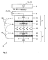
- Fig. 1 illustrates a random access memory (MRAM) element 1 according to an embodiment.
- the MRAM element 1 comprises a magnetic tunnel junction 2 having a first portion 2' comprising a first storage layer 23 having a first storage magnetization 231; a first sense layer 21 having a first free magnetization 211; and a first tunnel barrier layer 25 between the first storage layer 23 and the first sense layer 21.
- the magnetic tunnel junction 2 further comprises a second portion 2" comprising a second storage layer 24 having a second storage magnetization 232; a second sense layer 22 having a second free magnetization 212; and a second tunnel barrier layer 26 between the second storage layer 24 and the second sense layer 22.
- the magnetic tunnel junction 2 further comprises an antiferromagnetic layer 20 comprised between the first and second storage layers 23, 24 and pinning the first and second storage magnetizations 231, 232 at a low temperature threshold, below a critical temperature of the antiferromagnetic layer 20, and freeing the first and second storage magnetizations 231, 232 at a high temperature threshold, at and above the critical temperature.
- a thermally-assisted (TA) write operation of the MRAM element 1 can comprise the step of:
- the configuration of the magnetic tunnel junction 2, where the first and second storage layers 23, 24 are symmetrically arranged on each side of the antiferromagnetic layer 20 results in that the first storage magnetization 231 is switched substantially simultaneously and in a direction substantially parallel to the second storage magnetization 232.
- the MRAM element 1 further comprises a field line 5 in communication with the magnetic tunnel junction 2.
- the field line 5 is arranged for passing a field current 51 adapted to generate a write magnetic field 52 that is able to switch the first and second storage magnetizations 231, 232 along a direction that is substantially perpendicular with the field line 5.
- Heating the MRAM element 1 can be performed by passing a heating current 31 in the magnetic tunnel junction 2 via a current line 4 in electrical communication with the magnetic tunnel junction 2 (see Fig. 1 ).
- the current line 4 could be also used for passing the field current 51 destined to generate the write magnetic field 52.
- the first and second storage layers 23, 24 are configured such as to have a magnetic anisotropy being oriented in a direction being substantially perpendicular with the field line 5 such that the first and second storage magnetizations 231, 232 are switched substantially simultaneously and substantially in the same direction by applying the write magnetic field 52.
- switching the first and second storage magnetizations 231, 232 is performed by applying the magnetic field 52 with a magnitude such as to saturate the first free magnetization 211 in a direction according to the direction of the write magnetic field 52.
- the saturated first free magnetization 211 induces in turn a first local magnetic stray field 60 coupling the first storage magnetization 231 in a closed magnetic flux configuration such as to orient the first storage magnetization 231 in the direction of the saturated first free magnetization 211.
- the magnetic field 52 is also arranged such as to saturate the second sense magnetization 212 in the direction of the write magnetic field 52.
- the saturated second sense magnetization 212 induces a second local magnetic stray field 61 magnetically coupling the second free magnetization 212 with the storage magnetization 232 in a closed magnetic flux configuration such as to orient the second storage magnetization 232 in the direction of the saturated second free magnetization 212.
- the first and second local magnetic stray fields 60, 61 are represented orienting the first and second storage magnetization toward the right.
- first and second local magnetic stray fields 60, 61 are oriented in the same direction, the first local magnetic stray field 60 also orients the second storage magnetization 232 in the direction of the saturated first free magnetization 211 and the second local magnetic stray field 61 orients the first storage magnetization 231 in the direction of the saturated second free magnetization 212.
- the first and second storage magnetization 231, 232 is then switched in accordance to a net magnetic stray field corresponding to the sum of the first magnetic stray field 60 and second local magnetic stray field 61.
- the first and second free magnetizations 211, 212, and thus the magnitude of the first and second local magnetic stray fields 60, 61 can be varied by varying the thickness of the first and second free layers 21, 22.
- the thickness of the first and second sense layers 21, 22 is such that each of the first and second free magnetizations 211, 212 is greater than the sum of the first and second storage magnetizations 231, 232.
- the thickness of the sense layer 21 is such that the magnitude of the write magnetic field 52 required for saturating the free magnetizations 211, 212 can be below about 80 Oe.
- the magnitude of the local magnetic stray field 60, 61 can be further increased by providing the sense layer 21, 24 with a material that exhibits large spontaneous magnetization.
- the magnitude of the write magnetic field 52 required for saturating the free magnetizations 211, 212 can be further reduced by providing the sense layer 21, 22 with a small anisotropy.
- the first and second storage magnetizations 231, 232 are more effectively coupled with the first and second free magnetizations 211, 212 than with the write magnetic field 52 generated by the field line 5 (or current line 4).
- a self-referenced method for reading the MRAM element 1 comprises:
- adjusting the first and second sense magnetizations 211, 212 in the first read direction comprises applying a read magnetic field 54 having a first direction by passing a read field current 53 with a first polarity in the field line 5.
- Adjusting the first and second sense magnetizations 211, 212 in the second read direction comprises applying the read magnetic field 54 having a second direction by passing the read current 53 with a second polarity in the field line 5.
- the first and second sense layers 21, 22 are configured such as to have a magnetic anisotropy being oriented in a direction being substantially perpendicular with the field line 5 such that the first and second sense magnetizations 211, 212 become adjusted substantially simultaneously and substantially in the same first and second direction when applying the read magnetic field 54 in the first and second direction, respectively.
- Measuring the first and second junction resistance values R 1 , R 2 can be performed by passing a sense current 32 in the magnetic tunnel junction 2 via the current line 4.
- the MRAM element 1 is being further configured such that the first portion 2' of the magnetic tunnel junction 2 has a first resistance-area product RA 1 that is substantially equal to a second resistance-area product RA 2 of the second portion 2" of the magnetic tunnel junction 2. Since during the write operation, the first storage magnetization 231 is switched in a direction substantially parallel to the second storage magnetization 232, the magnetoresistance ratio MR of the MRAM element 1 remains substantially unchanged by the write operation.
- MR magnetoresistance ratio
- R 1 is a low resistance of the magnetic tunnel junction 2 measured when the first and second sense magnetizations 211, 212 are adjusted substantially parallel to the first and second storage magnetizations 231, 232
- R 2 is a high resistance of the magnetic tunnel junction 2 measured when the first and second sense magnetizations 211, 212 are adjusted substantially antiparallel to the first and second storage magnetizations 231, 232.
- first and second tunnel barrier layers 25, 26 comprise Al 2 O 3 or MgO.
- the first and second tunnel barrier layers 25, 26 may have substantially the same thickness.
- the first and second sense layers 21, 22 can also have substantially the same thickness.
Landscapes
- Engineering & Computer Science (AREA)
- Computer Hardware Design (AREA)
- Chemical & Material Sciences (AREA)
- Crystallography & Structural Chemistry (AREA)
- Power Engineering (AREA)
- Manufacturing & Machinery (AREA)
- Mram Or Spin Memory Techniques (AREA)
- Hall/Mr Elements (AREA)
- Semiconductor Memories (AREA)
Abstract
Description
- The present invention concerns a random access memory (MRAM) element suitable for a thermally-assisted write operation and for a self-referenced read operation that can be reliably written at higher temperatures relative to conventional MRAM cells.
- Magnetic random access memory (MRAM) cells using the so-called self-referenced reading operation typically comprise a magnetic tunnel junction formed of a magnetic storage layer having a magnetization which direction can be changed from a first stable direction to a second stable direction, a thin insulating layer, and a sense layer with a magnetization having a reversible direction. Self-referenced MRAM cells allows for performing the write and read operation with low power consumption and an increased speed. The self-referenced reading operation is described in European patent application
EP 2276034 by the same applicant. It typically comprises as double sampling wherein the direction of sense layer magnetization is aligned in a first and second directions and the respective resistance of the magnetic tunnel junction is measured for each direction. - Self-referenced MRAM cells can be advantageously used in MRAM-based CAM, non-volatile cells for security applications including user privilege, security or encryption information on a packet-by-packet basis for high-performance data switches, firewalls, bridges, and routers. Self-referenced MRAM cells are also useful for making functional memories with a reduced yield as well as for high temperature applications.
- In the case of high temperature applications, a current pulse is passed through the magnetic tunnel junction in order to heat the MRAM cell to the high temperature. This current pulse is liable to subject the thin insulating layer to a considerable electric stress. The voltage applied through the magnetic tunnel junction could possibly reach or even exceed the breakdown voltage of such insulating layer. Even if the voltage applied across the insulating layer is lower than its breakdown voltage, the stress linked to the electric current pulse can result in considerable ageing effects in the long term, notably after a great number of voltage cycles, for example during writing cycles.
- The present disclosure concerns a magnetic random access memory (MRAM) element suitable for a thermally-assisted (TA) write operation and for a self-referenced read operation, comprising a magnetic tunnel junction portion having a first portion comprising: a first storage layer having a first storage magnetization; a first sense layer having a first free magnetization; and a first tunnel barrier layer between the first storage layer and the first sense layer; and a second portion, comprising: a second storage layer having a first storage magnetization; a second sense layer having a second free magnetization; and a second tunnel barrier layer between the second storage layer and the second sense layer; the magnetic tunnel junction portion further comprising an antiferromagnetic layer comprised between the first and second storage layers and pinning the first and second storage magnetizations at a low temperature threshold, and freeing the first and second storage magnetizations at a high temperature threshold; wherein during a write operation, the first and second free magnetization are magnetically saturable according to a direction of a write magnetic field when the write magnetic field is applied; and wherein the first and second storage magnetization are switchable in a direction substantially parallel and corresponding to the direction of the saturated first and second free magnetizations.
- In an embodiment, the MRAM element can be further configured such that the first magnetic tunnel junction portion has a first resistance-area product that is substantially equal to a second resistance-area product of the second magnetic tunnel junction portion, such that a magnetoresistance ratio of the MRAM element remains substantially unchanged during the write operation.
- The present disclosure further pertains to a method for writing to the MRAM element using the TA write operation, comprising:
- heating the magnetic tunnel junction at the high temperature threshold;
- switching the first and second storage magnetizations; and
- cooling the MRAM element below the critical temperature such as to freeze the first and second storage magnetizations in their written state; wherein the first and second storage magnetizations are switched substantially simultaneously in a direction substantially parallel to each other. Said switching can comprise applying a write magnetic field such as to magnetically saturate the first and second free magnetization according to a direction of the write magnetic field; and the first and second storage magnetizations can be switched substantially simultaneously in a direction substantially parallel to each other.
- The configuration of the disclosed MRAM element with the magnetic tunnel junction comprising the first and second tunnel barrier layers allows for reducing the voltage applied on the first and second tunnel barrier layers when the magnetic tunnel junction is heated the high temperature threshold, compared to a magnetic tunnel junction comprising only one barrier layer. The magnetic tunnel junction of the disclosed MRAM element can thus be heated effectively while minimizing risks of breakdown and ageing of the tunnel barrier layers.
- The invention will be better understood with the aid of the description of an embodiment given by way of example and illustrated by
figure 1 illustrating a random access memory element according to an embodiment. -
Fig. 1 illustrates a random access memory (MRAM)element 1 according to an embodiment. TheMRAM element 1 comprises amagnetic tunnel junction 2 having a first portion 2' comprising afirst storage layer 23 having a first storage magnetization 231; afirst sense layer 21 having a firstfree magnetization 211; and a firsttunnel barrier layer 25 between thefirst storage layer 23 and thefirst sense layer 21. Themagnetic tunnel junction 2 further comprises asecond portion 2" comprising asecond storage layer 24 having asecond storage magnetization 232; asecond sense layer 22 having a secondfree magnetization 212; and a secondtunnel barrier layer 26 between thesecond storage layer 24 and thesecond sense layer 22. Themagnetic tunnel junction 2 further comprises anantiferromagnetic layer 20 comprised between the first andsecond storage layers second storage magnetizations 231, 232 at a low temperature threshold, below a critical temperature of theantiferromagnetic layer 20, and freeing the first andsecond storage magnetizations 231, 232 at a high temperature threshold, at and above the critical temperature. - In an embodiment, a thermally-assisted (TA) write operation of the
MRAM element 1 can comprise the step of: - heating the
magnetic tunnel junction 2 to the high temperature threshold; - switching the first and
second storage magnetizations 231, 232; and; - cooling the
magnetic tunnel junction 2 at the low temperature threshold, such as to freeze the first andsecond storage magnetizations 231, 232 in their written state. - The configuration of the
magnetic tunnel junction 2, where the first andsecond storage layers antiferromagnetic layer 20 results in that the first storage magnetization 231 is switched substantially simultaneously and in a direction substantially parallel to thesecond storage magnetization 232. - In an embodiment, the
MRAM element 1 further comprises afield line 5 in communication with themagnetic tunnel junction 2. Thefield line 5 is arranged for passing a field current 51 adapted to generate a write magnetic field 52 that is able to switch the first andsecond storage magnetizations 231, 232 along a direction that is substantially perpendicular with thefield line 5. Heating theMRAM element 1 can be performed by passing a heating current 31 in themagnetic tunnel junction 2 via acurrent line 4 in electrical communication with the magnetic tunnel junction 2 (seeFig. 1 ). Alternatively, thecurrent line 4 could be also used for passing the field current 51 destined to generate the write magnetic field 52. Once themagnetic tunnel junction 2 has been cooled to the low temperature threshold, the storage magnetization 231 becomes pinned in the switched, or written, orientation in accordance with the orientation of the write magnetic field 52. - The first and
second storage layers field line 5 such that the first andsecond storage magnetizations 231, 232 are switched substantially simultaneously and substantially in the same direction by applying the write magnetic field 52. - In another embodiment, switching the first and
second storage magnetizations 231, 232 is performed by applying the magnetic field 52 with a magnitude such as to saturate the firstfree magnetization 211 in a direction according to the direction of the write magnetic field 52. The saturated firstfree magnetization 211 induces in turn a first localmagnetic stray field 60 coupling the first storage magnetization 231 in a closed magnetic flux configuration such as to orient the first storage magnetization 231 in the direction of the saturated firstfree magnetization 211. The magnetic field 52 is also arranged such as to saturate thesecond sense magnetization 212 in the direction of the write magnetic field 52. The saturatedsecond sense magnetization 212 induces a second localmagnetic stray field 61 magnetically coupling the secondfree magnetization 212 with thestorage magnetization 232 in a closed magnetic flux configuration such as to orient thesecond storage magnetization 232 in the direction of the saturated secondfree magnetization 212. InFig. 1 , the first and second localmagnetic stray fields magnetic stray fields magnetic stray field 60 also orients thesecond storage magnetization 232 in the direction of the saturated firstfree magnetization 211 and the second localmagnetic stray field 61 orients the first storage magnetization 231 in the direction of the saturated secondfree magnetization 212. The first andsecond storage magnetization 231, 232 is then switched in accordance to a net magnetic stray field corresponding to the sum of the firstmagnetic stray field 60 and second localmagnetic stray field 61. - The first and second
free magnetizations magnetic stray fields free layers second sense layers free magnetizations second storage magnetizations 231, 232. Preferably, the thickness of thesense layer 21 is such that the magnitude of the write magnetic field 52 required for saturating thefree magnetizations magnetic stray field sense layer free magnetizations sense layer - Since the distance between the
first storage layer 23 and thefirst sense layer 21, and between thesecond storage layer 24 and thesecond sense layer 22 is small, typically in the nanometer range, the first andsecond storage magnetizations 231, 232 are more effectively coupled with the first and secondfree magnetizations - In another embodiment, a self-referenced method for reading the
MRAM element 1 comprises: - adjusting the first and
second sense magnetizations - measuring a first junction resistance value R1;
- adjusting the first and
second sense magnetizations - measuring a second junction resistance value R2.
- In an embodiment, adjusting the first and
second sense magnetizations field line 5. Adjusting the first andsecond sense magnetizations field line 5. The first andsecond sense layers field line 5 such that the first andsecond sense magnetizations magnetic tunnel junction 2 via thecurrent line 4. - The
MRAM element 1 is being further configured such that the first portion 2' of themagnetic tunnel junction 2 has a first resistance-area product RA1 that is substantially equal to a second resistance-area product RA2 of thesecond portion 2" of themagnetic tunnel junction 2. Since during the write operation, the first storage magnetization 231 is switched in a direction substantially parallel to thesecond storage magnetization 232, the magnetoresistance ratio MR of theMRAM element 1 remains substantially unchanged by the write operation. Here the magnetoresistance ratio MR is defined as:
where R1 is a low resistance of themagnetic tunnel junction 2 measured when the first andsecond sense magnetizations second storage magnetizations 231, 232, and R2 is a high resistance of themagnetic tunnel junction 2 measured when the first andsecond sense magnetizations second storage magnetizations 231, 232. - In an embodiment, the first and second tunnel barrier layers 25, 26 comprise Al2O3 or MgO. The first and second tunnel barrier layers 25, 26 may have substantially the same thickness. The first and second sense layers 21, 22 can also have substantially the same thickness.
-
- 1
- magnetic random access memory cell
- 2
- magnetic tunnel junction
- 2'
- first portion
- 2"
- second portion
- 20
- antiferromagnetic layer
- 21
- first sense layer
- 22
- second sense layer
- 23
- first storage layer
- 24
- second storage layer
- 25
- first tunnel barrier layer
- 26
- second tunnel barrier layer
- 211
- first free magnetization
- 212
- second free magnetization
- 231
- first ferromagnetic layer
- 232
- second ferromagnetic layer
- 24
- first antiferromagnetic layer
- 31
- heating current
- 32
- read current
- 4
- current line
- 5
- field line
- 51
- write current
- 52
- write magnetic field
- 53
- read field current
- 54
- read magnetic field
- 60
- first local magnetic stray field
- 61
- second local magnetic stray field
- MR
- magnetoresistance ratio
- R1
- low resistance
- R2
- high resistance
- RA1
- first resistance-area product
- RA2
- second resistance-area product
Claims (9)
- Magnetic random access memory (MRAM) element (1) suitable for a thermally-assisted (TA) write operation and for a self-referenced read operation and having a magnetoresistance ratio (MR), the MRAM element (1) comprising a magnetic tunnel junction portion (2) having a first portion (2') comprising:a first storage layer (23) having a first storage magnetization (231);a first sense layer (21) having a first free magnetization (211); anda first tunnel barrier layer (25) between the first storage layer (23) and the first sense layer (21);and a second portion (2"), comprising:a second storage layer (24) having a second storage magnetization (232);a second sense layer (22) having a second free magnetization (212); anda second tunnel barrier layer (26) between the second storage layer (24) and the second sense layer (22);the magnetic tunnel junction portion (2) further comprising an antiferromagnetic layer (20) comprised between the first and second storage layers (23, 24) and pinning the first and second storage magnetizations (231, 232) at a low temperature threshold, and freeing the first and second storage magnetizations (231, 232) at a high temperature threshold; characterized in thatduring a write operation, the first and second free magnetization (211, 212) are magnetically saturable according to a direction of a write magnetic field (52) when the write magnetic field (52) is applied; and in thatthe first and second storage magnetization (231, 232) are switchable in a direction substantially parallel and corresponding to the direction of the saturated first and second free magnetizations (211, 212).
- MRAM element (1) according to claim 1, being further configured such that during a read operation the first and second free magnetizations (211, 212) are adjusted substantially simultaneously and in a direction substantially parallel.
- MRAM element (1) according to the claims 1 or 2,
being further configured such that the first magnetic tunnel junction portion (2) has a first resistance-area product (RA1) that is substantially equal to a second resistance-area product (RA2) of the second magnetic tunnel junction portion (2'), such that a magnetoresistance ratio of the MRAM element (1) remains substantially unchanged during the write operation. - MRAM element (1) according to any one of claims 1 to 3,
wherein
the first and second tunnel barrier layers (25, 26) comprise Al2O3 or MgO. - MRAM element (1) according to to any one of claims 1 to 4,
wherein
the first and second tunnel barrier layers (25, 26) have substantially the same thickness. - A method for writing to the MRAM element (1) characterized by any one of claims 1 to 5 using the TA write operation, comprising:heating the MRAM element (1) at the high temperature threshold;switching the first and second storage magnetizations (231, 232); andcooling the MRAM element (1) at the low temperature threshold such as to freeze the first and second storage magnetizations (231, 232) in their written state; characterized in thatsaid switching comprising applying a write magnetic field (52) such as to magnetically saturate the first and second free magnetization (211, 212) according to a direction of the write magnetic field (52); and in thatthe first and second storage magnetizations (231, 232) are switched substantially simultaneously in a direction substantially parallel to each other.
- Method for writing according to claim 6, wherein
the MRAM element (1) further comprises a field line (5) in communication with the first and second magnetic tunnel junction portions (2, 2') and
wherein
said switching first and second storage magnetizations (231, 232) is performed by a magnetic field (52) generated by passing a field current (51) through the field line (5). - A method for reading the MRAM element (1) characterized by any one of claims 1 to 5, comprising:adjusting the first and second free magnetizations (211, 212) in a first read direction;measuring a first junction resistance value (R1);adjusting the first and second free magnetizations (211, 212) in a second read direction; andmeasuring a second junction resistance value (R2), wherein said adjusting the first and second free magnetizations (211, 212) is performed simultaneously.
- Method for reading according to claim 8, wherein
the MRAM element (1) further comprises a field line (5) in communication with the first and second magnetic tunnel junction portions (2, 2') and
wherein
said adjusting the first and second free magnetizations (211, 212) in a first read direction and in a second direction comprises applying a read magnetic field (54) by passing a read current (53) in the field line (5), the read magnetic field (54) having a first direction and a second direction opposed to the first direction, respectively.
Priority Applications (1)
| Application Number | Priority Date | Filing Date | Title |
|---|---|---|---|
| EP12007861.3A EP2597693B1 (en) | 2011-11-22 | 2012-11-21 | Self-referenced MRAM cell with optimized reliability |
Applications Claiming Priority (2)
| Application Number | Priority Date | Filing Date | Title |
|---|---|---|---|
| EP11290533.6A EP2597692A1 (en) | 2011-11-22 | 2011-11-22 | Self-referenced MRAM cell with optimized reliability |
| EP12007861.3A EP2597693B1 (en) | 2011-11-22 | 2012-11-21 | Self-referenced MRAM cell with optimized reliability |
Publications (2)
| Publication Number | Publication Date |
|---|---|
| EP2597693A1 true EP2597693A1 (en) | 2013-05-29 |
| EP2597693B1 EP2597693B1 (en) | 2017-06-07 |
Family
ID=45491346
Family Applications (2)
| Application Number | Title | Priority Date | Filing Date |
|---|---|---|---|
| EP11290533.6A Withdrawn EP2597692A1 (en) | 2011-11-22 | 2011-11-22 | Self-referenced MRAM cell with optimized reliability |
| EP12007861.3A Active EP2597693B1 (en) | 2011-11-22 | 2012-11-21 | Self-referenced MRAM cell with optimized reliability |
Family Applications Before (1)
| Application Number | Title | Priority Date | Filing Date |
|---|---|---|---|
| EP11290533.6A Withdrawn EP2597692A1 (en) | 2011-11-22 | 2011-11-22 | Self-referenced MRAM cell with optimized reliability |
Country Status (7)
| Country | Link |
|---|---|
| US (1) | US8885397B2 (en) |
| EP (2) | EP2597692A1 (en) |
| JP (1) | JP2013110417A (en) |
| KR (1) | KR20130056840A (en) |
| CN (1) | CN103137856B (en) |
| RU (1) | RU2591643C2 (en) |
| TW (1) | TWI529986B (en) |
Families Citing this family (6)
| Publication number | Priority date | Publication date | Assignee | Title |
|---|---|---|---|---|
| KR20130018470A (en) * | 2011-08-09 | 2013-02-25 | 에스케이하이닉스 주식회사 | Semiconductor device |
| US20150129946A1 (en) * | 2013-11-13 | 2015-05-14 | International Business Machines Corporation | Self reference thermally assisted mram with low moment ferromagnet storage layer |
| EP2958108B1 (en) * | 2014-06-17 | 2019-08-28 | CROCUS Technology | Self-referenced multibit MRAM cell having a synthetic antiferromagnetic storage layer |
| EP3023803B1 (en) * | 2014-11-19 | 2020-03-18 | Crocus Technology S.A. | MLU cell for sensing an external magnetic field and a magnetic sensor device comprising the MLU cell |
| US9799387B1 (en) * | 2016-12-21 | 2017-10-24 | Globalfoundries Singapore Pte. Ltd. | Integrated circuits with programmable memory cells and methods for programming the same |
| TWI764313B (en) * | 2020-10-12 | 2022-05-11 | 素國 霍 | Hybrid perpendicular and in-plane stt-mram |
Citations (5)
| Publication number | Priority date | Publication date | Assignee | Title |
|---|---|---|---|---|
| US5869963A (en) * | 1996-09-12 | 1999-02-09 | Alps Electric Co., Ltd. | Magnetoresistive sensor and head |
| US20050180202A1 (en) * | 2004-02-13 | 2005-08-18 | Yiming Huai | Method and system for providing heat assisted switching of a magnetic element utilizing spin transfer |
| US20060102969A1 (en) * | 2004-11-16 | 2006-05-18 | Yiming Huai | Spin scattering and heat assisted switching of a magnetic element |
| US7796428B2 (en) * | 2007-12-21 | 2010-09-14 | Commissariat A L'energie Atomique | Thermally assisted magnetic write memory |
| EP2276034A2 (en) | 2009-07-13 | 2011-01-19 | Crocus Technology S.A. | Self-referenced magnetic random access memory cell |
Family Cites Families (8)
| Publication number | Priority date | Publication date | Assignee | Title |
|---|---|---|---|---|
| JP4050446B2 (en) * | 2000-06-30 | 2008-02-20 | 株式会社東芝 | Solid state magnetic memory |
| US6822838B2 (en) * | 2002-04-02 | 2004-11-23 | International Business Machines Corporation | Dual magnetic tunnel junction sensor with a longitudinal bias stack |
| JP3935049B2 (en) * | 2002-11-05 | 2007-06-20 | 株式会社東芝 | Magnetic storage device and manufacturing method thereof |
| JP3766380B2 (en) * | 2002-12-25 | 2006-04-12 | 株式会社東芝 | Magnetic random access memory and data read method of the magnetic random access memory |
| US6667901B1 (en) * | 2003-04-29 | 2003-12-23 | Hewlett-Packard Development Company, L.P. | Dual-junction magnetic memory device and read method |
| US7180113B2 (en) * | 2005-02-10 | 2007-02-20 | Infineon Technologies Ag | Double-decker MRAM cell with rotated reference layer magnetizations |
| RU2367057C2 (en) * | 2007-10-31 | 2009-09-10 | Государственное образовательное учреждение высшего профессионального образования "Московский Инженерно-Физический Институт (государственный университет)" | Method of forming structures of magnetic tunnel barriers for magnetoresistive random access magnetic memory and structure of magnetic tunnel barrier for magnetoresistive random access magnetic memory (versions) |
| US8406041B2 (en) * | 2009-07-08 | 2013-03-26 | Alexander Mikhailovich Shukh | Scalable magnetic memory cell with reduced write current |
-
2011
- 2011-11-22 EP EP11290533.6A patent/EP2597692A1/en not_active Withdrawn
-
2012
- 2012-11-21 EP EP12007861.3A patent/EP2597693B1/en active Active
- 2012-11-21 US US13/683,239 patent/US8885397B2/en active Active
- 2012-11-22 JP JP2012256066A patent/JP2013110417A/en active Pending
- 2012-11-22 CN CN201210533712.0A patent/CN103137856B/en not_active Expired - Fee Related
- 2012-11-22 TW TW101143650A patent/TWI529986B/en not_active IP Right Cessation
- 2012-11-22 RU RU2012150042/08A patent/RU2591643C2/en not_active IP Right Cessation
- 2012-11-22 KR KR1020120133024A patent/KR20130056840A/en not_active Withdrawn
Patent Citations (5)
| Publication number | Priority date | Publication date | Assignee | Title |
|---|---|---|---|---|
| US5869963A (en) * | 1996-09-12 | 1999-02-09 | Alps Electric Co., Ltd. | Magnetoresistive sensor and head |
| US20050180202A1 (en) * | 2004-02-13 | 2005-08-18 | Yiming Huai | Method and system for providing heat assisted switching of a magnetic element utilizing spin transfer |
| US20060102969A1 (en) * | 2004-11-16 | 2006-05-18 | Yiming Huai | Spin scattering and heat assisted switching of a magnetic element |
| US7796428B2 (en) * | 2007-12-21 | 2010-09-14 | Commissariat A L'energie Atomique | Thermally assisted magnetic write memory |
| EP2276034A2 (en) | 2009-07-13 | 2011-01-19 | Crocus Technology S.A. | Self-referenced magnetic random access memory cell |
Non-Patent Citations (1)
| Title |
|---|
| WANG JIANGUO ET AL: "Low-current blocking temperature writing of double barrier magnetic random access memory cells", APPLIED PHYSICS LETTERS, AIP, AMERICAN INSTITUTE OF PHYSICS, MELVILLE, NY, US, vol. 84, no. 6, 9 February 2004 (2004-02-09), pages 945 - 947, XP012062056, ISSN: 0003-6951, DOI: 10.1063/1.1646211 * |
Also Published As
| Publication number | Publication date |
|---|---|
| US20130128659A1 (en) | 2013-05-23 |
| CN103137856A (en) | 2013-06-05 |
| EP2597692A1 (en) | 2013-05-29 |
| RU2591643C2 (en) | 2016-07-20 |
| JP2013110417A (en) | 2013-06-06 |
| TWI529986B (en) | 2016-04-11 |
| EP2597693B1 (en) | 2017-06-07 |
| KR20130056840A (en) | 2013-05-30 |
| US8885397B2 (en) | 2014-11-11 |
| TW201342677A (en) | 2013-10-16 |
| RU2012150042A (en) | 2014-05-27 |
| CN103137856B (en) | 2017-03-01 |
Similar Documents
| Publication | Publication Date | Title |
|---|---|---|
| EP2249350B1 (en) | Magnetic memory with a thermally assisted spin transfer torque writing procedure using a low writing current | |
| EP2477227B1 (en) | Magnetic tunnel junction comprising a polarizing layer | |
| EP2575135B1 (en) | Magnetic random access memory (MRAM) cell and method for reading the MRAM cell using a self-referenced read operation | |
| EP2605246B1 (en) | Self-referenced magnetic random access memory element comprising a synthetic storage layer | |
| EP2597693B1 (en) | Self-referenced MRAM cell with optimized reliability | |
| EP2725580B1 (en) | Thermally assisted MRAM cell and method for writing a plurality of bits in the MRAM cell | |
| EP2608208B1 (en) | Self-referenced MRAM cell and method for writing the cell using a spin transfer torque write operation | |
| EP2528060B1 (en) | Multibit cell with synthetic storage layer | |
| EP2575136B1 (en) | Self-reference magnetic random access memory (MRAM) cell comprising ferromagnetic layers | |
| EP2249349B1 (en) | Magnetic memory with a thermally assisted writing procedure and reduced writng field | |
| EP2942780A1 (en) | Multi-bit MRAM cell and method for writing and reading to such MRAM cell | |
| EP2626860B1 (en) | Self-referenced mram element with linear sensing signal | |
| US9305628B2 (en) | Self-referenced magnetic random access memory (MRAM) and method for writing to the MRAM cell with increased reliability and reduced power consumption | |
| US10115445B2 (en) | Magnetic memory device that is protected against reading using an external magnetic field and method for operating such magnetic memory device | |
| EP2958108B1 (en) | Self-referenced multibit MRAM cell having a synthetic antiferromagnetic storage layer | |
| EP2905783B1 (en) | Method for writing to a multibit TAS-MRAM device configured for self-referenced read operation with improved reproducibly |
Legal Events
| Date | Code | Title | Description |
|---|---|---|---|
| PUAI | Public reference made under article 153(3) epc to a published international application that has entered the european phase |
Free format text: ORIGINAL CODE: 0009012 |
|
| AK | Designated contracting states |
Kind code of ref document: A1 Designated state(s): AL AT BE BG CH CY CZ DE DK EE ES FI FR GB GR HR HU IE IS IT LI LT LU LV MC MK MT NL NO PL PT RO RS SE SI SK SM TR |
|
| AX | Request for extension of the european patent |
Extension state: BA ME |
|
| 17P | Request for examination filed |
Effective date: 20131113 |
|
| RBV | Designated contracting states (corrected) |
Designated state(s): AL AT BE BG CH CY CZ DE DK EE ES FI FR GB GR HR HU IE IS IT LI LT LU LV MC MK MT NL NO PL PT RO RS SE SI SK SM TR |
|
| 17Q | First examination report despatched |
Effective date: 20150508 |
|
| REG | Reference to a national code |
Ref country code: DE Ref legal event code: R079 Ref document number: 602012033145 Country of ref document: DE Free format text: PREVIOUS MAIN CLASS: H01L0043080000 Ipc: H01F0010320000 |
|
| RIC1 | Information provided on ipc code assigned before grant |
Ipc: G11C 11/16 20060101ALI20161006BHEP Ipc: H01L 43/08 20060101ALI20161006BHEP Ipc: H01F 10/32 20060101AFI20161006BHEP Ipc: H01L 43/12 20060101ALI20161006BHEP |
|
| GRAP | Despatch of communication of intention to grant a patent |
Free format text: ORIGINAL CODE: EPIDOSNIGR1 |
|
| STAA | Information on the status of an ep patent application or granted ep patent |
Free format text: STATUS: GRANT OF PATENT IS INTENDED |
|
| RAP1 | Party data changed (applicant data changed or rights of an application transferred) |
Owner name: CROCUS TECHNOLOGY S.A. |
|
| INTG | Intention to grant announced |
Effective date: 20161122 |
|
| GRAJ | Information related to disapproval of communication of intention to grant by the applicant or resumption of examination proceedings by the epo deleted |
Free format text: ORIGINAL CODE: EPIDOSDIGR1 |
|
| STAA | Information on the status of an ep patent application or granted ep patent |
Free format text: STATUS: EXAMINATION IS IN PROGRESS |
|
| GRAS | Grant fee paid |
Free format text: ORIGINAL CODE: EPIDOSNIGR3 |
|
| STAA | Information on the status of an ep patent application or granted ep patent |
Free format text: STATUS: GRANT OF PATENT IS INTENDED |
|
| GRAP | Despatch of communication of intention to grant a patent |
Free format text: ORIGINAL CODE: EPIDOSNIGR1 |
|
| INTC | Intention to grant announced (deleted) | ||
| GRAA | (expected) grant |
Free format text: ORIGINAL CODE: 0009210 |
|
| STAA | Information on the status of an ep patent application or granted ep patent |
Free format text: STATUS: THE PATENT HAS BEEN GRANTED |
|
| INTG | Intention to grant announced |
Effective date: 20170419 |
|
| AK | Designated contracting states |
Kind code of ref document: B1 Designated state(s): AL AT BE BG CH CY CZ DE DK EE ES FI FR GB GR HR HU IE IS IT LI LT LU LV MC MK MT NL NO PL PT RO RS SE SI SK SM TR |
|
| REG | Reference to a national code |
Ref country code: GB Ref legal event code: FG4D |
|
| GRAA | (expected) grant |
Free format text: ORIGINAL CODE: 0009210 |
|
| REG | Reference to a national code |
Ref country code: CH Ref legal event code: EP Ref country code: AT Ref legal event code: REF Ref document number: 899761 Country of ref document: AT Kind code of ref document: T Effective date: 20170615 |
|
| REG | Reference to a national code |
Ref country code: IE Ref legal event code: FG4D |
|
| REG | Reference to a national code |
Ref country code: DE Ref legal event code: R096 Ref document number: 602012033145 Country of ref document: DE |
|
| REG | Reference to a national code |
Ref country code: NL Ref legal event code: MP Effective date: 20170607 |
|
| REG | Reference to a national code |
Ref country code: LT Ref legal event code: MG4D |
|
| PG25 | Lapsed in a contracting state [announced via postgrant information from national office to epo] |
Ref country code: FI Free format text: LAPSE BECAUSE OF FAILURE TO SUBMIT A TRANSLATION OF THE DESCRIPTION OR TO PAY THE FEE WITHIN THE PRESCRIBED TIME-LIMIT Effective date: 20170607 Ref country code: GR Free format text: LAPSE BECAUSE OF FAILURE TO SUBMIT A TRANSLATION OF THE DESCRIPTION OR TO PAY THE FEE WITHIN THE PRESCRIBED TIME-LIMIT Effective date: 20170908 Ref country code: NO Free format text: LAPSE BECAUSE OF FAILURE TO SUBMIT A TRANSLATION OF THE DESCRIPTION OR TO PAY THE FEE WITHIN THE PRESCRIBED TIME-LIMIT Effective date: 20170907 Ref country code: HR Free format text: LAPSE BECAUSE OF FAILURE TO SUBMIT A TRANSLATION OF THE DESCRIPTION OR TO PAY THE FEE WITHIN THE PRESCRIBED TIME-LIMIT Effective date: 20170607 Ref country code: LT Free format text: LAPSE BECAUSE OF FAILURE TO SUBMIT A TRANSLATION OF THE DESCRIPTION OR TO PAY THE FEE WITHIN THE PRESCRIBED TIME-LIMIT Effective date: 20170607 Ref country code: ES Free format text: LAPSE BECAUSE OF FAILURE TO SUBMIT A TRANSLATION OF THE DESCRIPTION OR TO PAY THE FEE WITHIN THE PRESCRIBED TIME-LIMIT Effective date: 20170607 |
|
| REG | Reference to a national code |
Ref country code: AT Ref legal event code: MK05 Ref document number: 899761 Country of ref document: AT Kind code of ref document: T Effective date: 20170607 |
|
| REG | Reference to a national code |
Ref country code: FR Ref legal event code: PLFP Year of fee payment: 6 |
|
| PG25 | Lapsed in a contracting state [announced via postgrant information from national office to epo] |
Ref country code: LV Free format text: LAPSE BECAUSE OF FAILURE TO SUBMIT A TRANSLATION OF THE DESCRIPTION OR TO PAY THE FEE WITHIN THE PRESCRIBED TIME-LIMIT Effective date: 20170607 Ref country code: SE Free format text: LAPSE BECAUSE OF FAILURE TO SUBMIT A TRANSLATION OF THE DESCRIPTION OR TO PAY THE FEE WITHIN THE PRESCRIBED TIME-LIMIT Effective date: 20170607 Ref country code: RS Free format text: LAPSE BECAUSE OF FAILURE TO SUBMIT A TRANSLATION OF THE DESCRIPTION OR TO PAY THE FEE WITHIN THE PRESCRIBED TIME-LIMIT Effective date: 20170607 Ref country code: NL Free format text: LAPSE BECAUSE OF FAILURE TO SUBMIT A TRANSLATION OF THE DESCRIPTION OR TO PAY THE FEE WITHIN THE PRESCRIBED TIME-LIMIT Effective date: 20170607 Ref country code: BG Free format text: LAPSE BECAUSE OF FAILURE TO SUBMIT A TRANSLATION OF THE DESCRIPTION OR TO PAY THE FEE WITHIN THE PRESCRIBED TIME-LIMIT Effective date: 20170907 |
|
| PG25 | Lapsed in a contracting state [announced via postgrant information from national office to epo] |
Ref country code: RO Free format text: LAPSE BECAUSE OF FAILURE TO SUBMIT A TRANSLATION OF THE DESCRIPTION OR TO PAY THE FEE WITHIN THE PRESCRIBED TIME-LIMIT Effective date: 20170607 Ref country code: SK Free format text: LAPSE BECAUSE OF FAILURE TO SUBMIT A TRANSLATION OF THE DESCRIPTION OR TO PAY THE FEE WITHIN THE PRESCRIBED TIME-LIMIT Effective date: 20170607 Ref country code: CZ Free format text: LAPSE BECAUSE OF FAILURE TO SUBMIT A TRANSLATION OF THE DESCRIPTION OR TO PAY THE FEE WITHIN THE PRESCRIBED TIME-LIMIT Effective date: 20170607 Ref country code: EE Free format text: LAPSE BECAUSE OF FAILURE TO SUBMIT A TRANSLATION OF THE DESCRIPTION OR TO PAY THE FEE WITHIN THE PRESCRIBED TIME-LIMIT Effective date: 20170607 Ref country code: AT Free format text: LAPSE BECAUSE OF FAILURE TO SUBMIT A TRANSLATION OF THE DESCRIPTION OR TO PAY THE FEE WITHIN THE PRESCRIBED TIME-LIMIT Effective date: 20170607 |
|
| PG25 | Lapsed in a contracting state [announced via postgrant information from national office to epo] |
Ref country code: SM Free format text: LAPSE BECAUSE OF FAILURE TO SUBMIT A TRANSLATION OF THE DESCRIPTION OR TO PAY THE FEE WITHIN THE PRESCRIBED TIME-LIMIT Effective date: 20170607 Ref country code: IS Free format text: LAPSE BECAUSE OF FAILURE TO SUBMIT A TRANSLATION OF THE DESCRIPTION OR TO PAY THE FEE WITHIN THE PRESCRIBED TIME-LIMIT Effective date: 20171007 Ref country code: PL Free format text: LAPSE BECAUSE OF FAILURE TO SUBMIT A TRANSLATION OF THE DESCRIPTION OR TO PAY THE FEE WITHIN THE PRESCRIBED TIME-LIMIT Effective date: 20170607 Ref country code: IT Free format text: LAPSE BECAUSE OF FAILURE TO SUBMIT A TRANSLATION OF THE DESCRIPTION OR TO PAY THE FEE WITHIN THE PRESCRIBED TIME-LIMIT Effective date: 20170607 |
|
| REG | Reference to a national code |
Ref country code: DE Ref legal event code: R097 Ref document number: 602012033145 Country of ref document: DE |
|
| PLBE | No opposition filed within time limit |
Free format text: ORIGINAL CODE: 0009261 |
|
| STAA | Information on the status of an ep patent application or granted ep patent |
Free format text: STATUS: NO OPPOSITION FILED WITHIN TIME LIMIT |
|
| PG25 | Lapsed in a contracting state [announced via postgrant information from national office to epo] |
Ref country code: DK Free format text: LAPSE BECAUSE OF FAILURE TO SUBMIT A TRANSLATION OF THE DESCRIPTION OR TO PAY THE FEE WITHIN THE PRESCRIBED TIME-LIMIT Effective date: 20170607 |
|
| 26N | No opposition filed |
Effective date: 20180308 |
|
| PG25 | Lapsed in a contracting state [announced via postgrant information from national office to epo] |
Ref country code: SI Free format text: LAPSE BECAUSE OF FAILURE TO SUBMIT A TRANSLATION OF THE DESCRIPTION OR TO PAY THE FEE WITHIN THE PRESCRIBED TIME-LIMIT Effective date: 20170607 |
|
| PG25 | Lapsed in a contracting state [announced via postgrant information from national office to epo] |
Ref country code: MC Free format text: LAPSE BECAUSE OF FAILURE TO SUBMIT A TRANSLATION OF THE DESCRIPTION OR TO PAY THE FEE WITHIN THE PRESCRIBED TIME-LIMIT Effective date: 20170607 |
|
| PG25 | Lapsed in a contracting state [announced via postgrant information from national office to epo] |
Ref country code: LI Free format text: LAPSE BECAUSE OF NON-PAYMENT OF DUE FEES Effective date: 20171130 Ref country code: CH Free format text: LAPSE BECAUSE OF NON-PAYMENT OF DUE FEES Effective date: 20171130 |
|
| PG25 | Lapsed in a contracting state [announced via postgrant information from national office to epo] |
Ref country code: LU Free format text: LAPSE BECAUSE OF NON-PAYMENT OF DUE FEES Effective date: 20171121 |
|
| REG | Reference to a national code |
Ref country code: BE Ref legal event code: MM Effective date: 20171130 |
|
| REG | Reference to a national code |
Ref country code: IE Ref legal event code: MM4A |
|
| PG25 | Lapsed in a contracting state [announced via postgrant information from national office to epo] |
Ref country code: MT Free format text: LAPSE BECAUSE OF NON-PAYMENT OF DUE FEES Effective date: 20171121 |
|
| PG25 | Lapsed in a contracting state [announced via postgrant information from national office to epo] |
Ref country code: IE Free format text: LAPSE BECAUSE OF NON-PAYMENT OF DUE FEES Effective date: 20171121 |
|
| PG25 | Lapsed in a contracting state [announced via postgrant information from national office to epo] |
Ref country code: BE Free format text: LAPSE BECAUSE OF NON-PAYMENT OF DUE FEES Effective date: 20171130 |
|
| PG25 | Lapsed in a contracting state [announced via postgrant information from national office to epo] |
Ref country code: HU Free format text: LAPSE BECAUSE OF FAILURE TO SUBMIT A TRANSLATION OF THE DESCRIPTION OR TO PAY THE FEE WITHIN THE PRESCRIBED TIME-LIMIT; INVALID AB INITIO Effective date: 20121121 |
|
| PG25 | Lapsed in a contracting state [announced via postgrant information from national office to epo] |
Ref country code: CY Free format text: LAPSE BECAUSE OF NON-PAYMENT OF DUE FEES Effective date: 20170607 |
|
| PG25 | Lapsed in a contracting state [announced via postgrant information from national office to epo] |
Ref country code: MK Free format text: LAPSE BECAUSE OF FAILURE TO SUBMIT A TRANSLATION OF THE DESCRIPTION OR TO PAY THE FEE WITHIN THE PRESCRIBED TIME-LIMIT Effective date: 20170607 |
|
| REG | Reference to a national code |
Ref country code: DE Ref legal event code: R082 Ref document number: 602012033145 Country of ref document: DE Representative=s name: BECK & ROESSIG EUROPEAN PATENT ATTORNEYS, DE Ref country code: DE Ref legal event code: R082 Ref document number: 602012033145 Country of ref document: DE Representative=s name: BECK & ROESSIG - EUROPEAN PATENT ATTORNEYS, DE |
|
| PG25 | Lapsed in a contracting state [announced via postgrant information from national office to epo] |
Ref country code: TR Free format text: LAPSE BECAUSE OF FAILURE TO SUBMIT A TRANSLATION OF THE DESCRIPTION OR TO PAY THE FEE WITHIN THE PRESCRIBED TIME-LIMIT Effective date: 20170607 |
|
| PG25 | Lapsed in a contracting state [announced via postgrant information from national office to epo] |
Ref country code: PT Free format text: LAPSE BECAUSE OF FAILURE TO SUBMIT A TRANSLATION OF THE DESCRIPTION OR TO PAY THE FEE WITHIN THE PRESCRIBED TIME-LIMIT Effective date: 20170607 |
|
| PG25 | Lapsed in a contracting state [announced via postgrant information from national office to epo] |
Ref country code: AL Free format text: LAPSE BECAUSE OF FAILURE TO SUBMIT A TRANSLATION OF THE DESCRIPTION OR TO PAY THE FEE WITHIN THE PRESCRIBED TIME-LIMIT Effective date: 20170607 |
|
| P01 | Opt-out of the competence of the unified patent court (upc) registered |
Effective date: 20230620 |
|
| REG | Reference to a national code |
Ref country code: DE Ref legal event code: R081 Ref document number: 602012033145 Country of ref document: DE Owner name: CROCUS TECHNOLOGY SA, FR Free format text: FORMER OWNER: CROCUS TECHNOLOGY S.A., GRENOBLE, FR Ref country code: DE Ref legal event code: R081 Ref document number: 602012033145 Country of ref document: DE Owner name: ALLEGRO MICRO SYSTEMS LLC, MANCHESTER, US Free format text: FORMER OWNER: CROCUS TECHNOLOGY S.A., GRENOBLE, FR Ref country code: DE Ref legal event code: R081 Ref document number: 602012033145 Country of ref document: DE Owner name: ALLEGRO MICRO SYSTEMS LLC, WILMINGTON, US Free format text: FORMER OWNER: CROCUS TECHNOLOGY S.A., GRENOBLE, FR |
|
| PGFP | Annual fee paid to national office [announced via postgrant information from national office to epo] |
Ref country code: GB Payment date: 20231123 Year of fee payment: 12 |
|
| REG | Reference to a national code |
Ref country code: DE Ref legal event code: R081 Ref document number: 602012033145 Country of ref document: DE Owner name: ALLEGRO MICRO SYSTEMS LLC, MANCHESTER, US Free format text: FORMER OWNER: CROCUS TECHNOLOGY SA, GRENOBLE, FR Ref country code: DE Ref legal event code: R081 Ref document number: 602012033145 Country of ref document: DE Owner name: ALLEGRO MICRO SYSTEMS LLC, WILMINGTON, US Free format text: FORMER OWNER: CROCUS TECHNOLOGY SA, GRENOBLE, FR |
|
| REG | Reference to a national code |
Ref country code: DE Ref legal event code: R081 Ref document number: 602012033145 Country of ref document: DE Owner name: ALLEGRO MICRO SYSTEMS LLC, MANCHESTER, US Free format text: FORMER OWNER: ALLEGRO MICRO SYSTEMS LLC, WILMINGTON, DE, US |
|
| REG | Reference to a national code |
Ref country code: GB Ref legal event code: 732E Free format text: REGISTERED BETWEEN 20240229 AND 20240306 |
|
| PGFP | Annual fee paid to national office [announced via postgrant information from national office to epo] |
Ref country code: FR Payment date: 20240909 Year of fee payment: 13 |
|
| PGFP | Annual fee paid to national office [announced via postgrant information from national office to epo] |
Ref country code: DE Payment date: 20240925 Year of fee payment: 13 |
|
| GBPC | Gb: european patent ceased through non-payment of renewal fee |
Effective date: 20241121 |
|
| PG25 | Lapsed in a contracting state [announced via postgrant information from national office to epo] |
Ref country code: GB Free format text: LAPSE BECAUSE OF NON-PAYMENT OF DUE FEES Effective date: 20241121 |