EP2595317A1 - Method to apply a modulation controlling the state of a switch - Google Patents
Method to apply a modulation controlling the state of a switch Download PDFInfo
- Publication number
- EP2595317A1 EP2595317A1 EP11306507.2A EP11306507A EP2595317A1 EP 2595317 A1 EP2595317 A1 EP 2595317A1 EP 11306507 A EP11306507 A EP 11306507A EP 2595317 A1 EP2595317 A1 EP 2595317A1
- Authority
- EP
- European Patent Office
- Prior art keywords
- switch
- circuitry
- modulation
- duty cycle
- rush current
- Prior art date
- Legal status (The legal status is an assumption and is not a legal conclusion. Google has not performed a legal analysis and makes no representation as to the accuracy of the status listed.)
- Withdrawn
Links
- 238000000034 method Methods 0.000 title claims abstract description 23
- 238000005516 engineering process Methods 0.000 description 6
- 239000003990 capacitor Substances 0.000 description 2
- 230000003247 decreasing effect Effects 0.000 description 2
- 238000004891 communication Methods 0.000 description 1
- 230000000295 complement effect Effects 0.000 description 1
- 230000007423 decrease Effects 0.000 description 1
- 238000002513 implantation Methods 0.000 description 1
- 239000004065 semiconductor Substances 0.000 description 1
- 230000003068 static effect Effects 0.000 description 1
Images

Classifications
-
- H—ELECTRICITY
- H03—ELECTRONIC CIRCUITRY
- H03K—PULSE TECHNIQUE
- H03K17/00—Electronic switching or gating, i.e. not by contact-making and –breaking
- H03K17/08—Modifications for protecting switching circuit against overcurrent or overvoltage
- H03K17/081—Modifications for protecting switching circuit against overcurrent or overvoltage without feedback from the output circuit to the control circuit
- H03K17/0814—Modifications for protecting switching circuit against overcurrent or overvoltage without feedback from the output circuit to the control circuit by measures taken in the output circuit
-
- H—ELECTRICITY
- H03—ELECTRONIC CIRCUITRY
- H03K—PULSE TECHNIQUE
- H03K17/00—Electronic switching or gating, i.e. not by contact-making and –breaking
- H03K17/08—Modifications for protecting switching circuit against overcurrent or overvoltage
- H03K17/082—Modifications for protecting switching circuit against overcurrent or overvoltage by feedback from the output to the control circuit
Definitions
- the invention relates to a method to apply a modulation controlling the state of a switch, a modulation circuitry, a set comprising a switch and the modulation circuitry, a circuitry package and a mobile phone adapted for carrying out the suggested use.
- CMOS Complementary metal-oxide-semiconductor
- CMOS technology is used in microprocessors, microcontrollers, static RAM, and other digital logic circuits.
- CMOS technology is also used for several analog circuits such as image sensors, data converters, and highly integrated transceivers for many types of communication.
- CMOS process technology also addresses problems linked to the field of sub-micron technology.
- leakage current is very high compared to other technologies.
- Specific power switch implementations are widespread to overcome this leakage problem in the case of the low power applications in integrated circuits.
- In-rush current is the maximum, instantaneous input current drawn by an electrical device when first turned on.
- the in-rush current depends notably on the capacitance of the switched domain. It is desirable to control this in-rush current.
- FIG. 1 it may be proposed a method wherein a relatively high impedance switch is first turned on and a relatively low impedance switch is then turned on.
- the circuitry 110 illustrated on Figure 1 comprises a supply pad 112 and the power domain 114 which is always fed up with power. Both supply pad 112 and power domain 114 are linked simultaneously to a high impedance switch 116 and to a low impedance switch 117.
- supply pad 112 and power domain 114 are in parallel with high impedance switch 16 and low impedance switch 117 which are respectively controlled by a first control circuit 119 and a second circuit 120.
- Such switch 116 and 117 are controlled to turn on one after another to provide power from the supply pad 112 and from power domain 114 to the zone 118 while avoiding in-rush current. Therefore, switch 116 and 117 can be labeled a power switch.
- Another solution may be to use an analog feedback loop to control the switch gate voltage to limit the peak current.
- the implementation of such loop implies an extra area for the analog control circuit.
- analog circuit is generally a larger area than a digital implementation.
- the object of the present invention is to alleviate at least partly the above mentioned drawbacks.
- the invention aims to propose a solution to reduce the in-rush current produced by a switch while limiting the extra area involved.
- This object is achieved with a method to apply a modulation controlling the state of a switch in a circuitry for modulating the equivalent resistance of the switch seen by the circuitry, so as to reduce the in-rush current created by switching on the switch in the circuitry.
- modulation circuitry controlling the state of a switch in a circuitry for modulating the equivalent resistance of the switch seen by the circuitry so as to reduce the in-rush current created by switching on the switch in the circuitry, the modulation circuitry being adapted to produce a modulation for which a duty cycle is defined, the duty cycle increasing with time from 1% to 100%, preferably 10% to 100%.
- the modulation circuitry may be adapted to carry out the method to apply as previously described.
- the modulation circuitry in such set may be adapted to carry out the method to apply as previously described.
- circuitry comprising such set and a mobile phone comprising the circuitry.
- the invention is based on a study of the appearance of the in-rush current, and more specifically the parameters which have an influence on this phenomenon.
- FIG 2 is a schematic view of a basic implementation of a circuitry with a power switch.
- the circuitry 10 illustrated on Figure 1 comprises a supply pad 12 and the power domain 14 which is always fed up with power. Both supply pad 12 and power domain 14 are linked to a switch 16.
- supply pad 12 and power domain 14 are in parallel with relation to switch 16.
- Such switch 16 enables to provide power from the supply pad 12 and from power domain 14 to the zone 18 to be provided with power. Therefore, switch 16 can be labeled a power switch.
- Switch 16 is enabled or disabled by a control circuit 19.
- circuitry 10 of Figure 1 is a circuitry comprising a supply voltage submitted to a resistor and a capacitor placed in series.
- the capacitance of the equivalent capacitor can be deduced from the area of the zone 18 to be provided with power.
- the resistance of the equivalent resistor comes from the switch 16 size.
- the peak current can be deduced from the area of the zone 18 to be provided with power, the supply voltage and the switch 16 size.
- the evolution of the decreasing exponential is linked to the inverse of the product of the capacitance by the resistance.
- the time evolution is run by the area of the zone 18 to be provided with power and the switch 16 size.
- the switch 16 size As the area of the zone 18 to be provided with power and the supply voltage depend on the circuitry 10 considered, it is suggested to modify the switch 16 size, at least the switch 16 size seen by circuitry 10.
- the method to apply a modulation controlling the state of the switch 16.
- state it should be understood that the switch 16 has at least two states, a state where zone 18 is provided with power and another state where zone 18 is not provided with power.
- modulation modulates the equivalent resistance of the switch 16 seen by circuitry 10, so as to reduce the in-rush current created by switching on switch 16 in circuitry 10.
- a modulation of the state of switch 16 enables to switch on and switch off switch 16 alternatively. Therefore, compared to a case where switch 16 is only switched on once (for instance the case of Figure 1 ), the modulation proposed enables to modulate the equivalence resistance of switch 16 seen by circuitry 10. Indeed, when switch 16 is switched off, resistance of switch 16 seen by circuitry 10 is equal to infinity. Thus, when considering a mean value, the resistance of switch 16 is increased compared to the case where switch 16 is only switched on. This results in a reduced in-rush current created by switching on switch 16 in circuitry 10. This avoids the problem linked to a too large in-rush current. Notably, the always on domain 14 will not get lower voltage and the risk of its failure decreases since the risk of not enough supply voltage is greatly reduced.
- circuitry 10 represented on Figure 3 .
- Such circuitry 10 comprises the elements of circuitry 10 of Figure 2 with a control circuit 20 substituted to the control circuit 19.
- the control circuit 20 is a modulation circuitry 20 comprising a modulation circuit 21 and adapted to control the state of switch 16 in circuitry 10 for modulating the equivalent resistance of the switch generated by the circuitry so as to reduce the in-rush current created by switching on switch 16 in circuitry 10.
- the size of the modulation circuitry 20 is very reduced compared to the control circuitry of the switch 116 and 117 which has to be used in the case of Figure 1 (prior art). Indeed, only digital circuitry is required. The use proposed therefore enables to reduce the in-rush current produced by a switch while limiting the extra area involved.
- the modulation employed in modulation circuitry 20 is preferably a modulation for which a duty cycle can be defined.
- the modulation can be divided in two states, an active state and an inactive state.
- the duty cycle is the ratio between the time spent by the modulation is in the active state and the total duration in time spent by the modulation is in both state (active and inactive).
- a low duty cycle (few percent for instance) corresponds to a low power because the modulation is mostly in the inactive state and a duty cycle of 100% corresponds to a case wherein the modulation is only in the active state.
- modulation circuitry 20 The modulation employed in modulation circuitry 20 is illustrated in Figure 5 .
- a pulse-width modulation (also named after its acronym PWM) is an example of modulation for which a duty cycle can be defined.
- a pulse-width modulation is also named a pulse-duration modulation (also named after its acronym PDM).
- Pulse-width modulation as illustrated in Figure 5 , uses a rectangular pulse wave whose pulse width is modulated resulting in the variation of the average of the waveform.
- the pulse-width of the first pulse, noted W 1 is corresponding to a low percentage of the period of the signal.
- the pulse width of second pulse, noted W 2 is corresponding is corresponding to a low percentage of the period of the signal so that W 1 ⁇ W 2 .
- pulse-widths are defined so that W i ⁇ W i+1 , where i varies between 1 (first pulse) to n, pulse-width W n corresponding to a duty cycle of 100%.
- Generating a pulse-width modulation can be made in a very easy way by the so-called "intersective method". According to this method, this can be carried out by using only sawtooth or a triangle waveform and a comparator. An oscillator is adapted to provide a sawtooth or a triangle waveform. In a more refined implementation, the characteristics of such pulse-width modulation are defined or optimized based on the equivalent capacitance and/or the equivalent resistance.
- the first duty cycle W 1 may be inferior to the duty cycle reached at a predetermined time W t .
- W t the equivalent resistance of switch 16 seen by circuitry 10 during the first duty cycle is then inferior to the equivalent resistance of switch 16 seen by circuitry 10 at the predetermined time. This results in a reduced in-rush current.
- the first duty cycle W 1 may be inferior to 10% and the duty cycle reached at a predetermined time W t may be superior to 80%. Indeed, with such values, the reduction obtained in the in-rush current is greatly enhanced. Mathematically both relations are fulfilled if W 1 > 10% and W t ⁇ 80%
- the duty cycle increases with time.
- the duty cycle may increases from 1% to 100%, preferably from 10% to 100%.
- the first period wherein the switch is in the on-state should be as short as possible. This enables to obtain a smooth evolution of the equivalent resistance of switch 16 seen by circuitry 10. As illustration, this first period lasts less than 100 ns, preferably less than 10 nanoseconds, more preferably less than 1 ns.
- Figure 6 represents the evolutions with time of in-rush current in the circuitry 10 of Figure 3 and according to the modulation applied by modulation circuitry 20 (see Figure 5 ).
- the modulation corresponds to curve 22 whereas the in-rush current corresponds to curve 24.
- the modulation applied in this case is a PWM modulation whose duty cycle increases with time and represented in Figure 5 .
- the in-rush current is greatly reduced as expected.
- In-rush current is now sliced in pulses whose width is corresponding to respective width pulse modulation. For example, a first modulation pulse (W1) with a duty cycle of 10% will lead to an in-rush current of 10% length.
- W1 first modulation pulse
- the method to apply a modulation enables the in-rush current to be cut, while the mean value of the in-rush current is lowered.
- the in-rush current is tailored so as to reach a mean value different from 0 and represented as a dash line 26.
- This enables to obtain a substantially constant in-rush current which can be used for a dedicated purpose. Therefore, the mean value of the in-rush current may be determined based on a desired application. This can result in reduction in power consumption. For instance, mean values of the in-rush current may be equal to 100 mA or to 10 mA.
- modulation circuitry 20 controlling the state of the switch 16 in circuitry 10 for modulating the equivalent resistance of switch 16 seen by circuitry 10 so as to reduce the in-rush current created by switching on switch 16 in circuitry 10.
- Modulation circuitry 20 is adapted to produce a modulation for which a duty cycle is defined, the duty cycle increasing with time from 1% to 100%, preferably 10% to 100%.
- Such modulation circuitry 20 may be employed for controlling a switch and obtaining a reduced in-rush current with a limited area involved.
- Such set may be included in a circuitry, the circuitry being for instance a circuitry adapted to be included in a mobile phone.
Landscapes
- Dc-Dc Converters (AREA)
Abstract
Description
- The invention relates to a method to apply a modulation controlling the state of a switch, a modulation circuitry, a set comprising a switch and the modulation circuitry, a circuitry package and a mobile phone adapted for carrying out the suggested use.
- Complementary metal-oxide-semiconductor (also labeled after its acronym CMOS) is a technology for constructing integrated circuits. CMOS technology is used in microprocessors, microcontrollers, static RAM, and other digital logic circuits. CMOS technology is also used for several analog circuits such as image sensors, data converters, and highly integrated transceivers for many types of communication.
- The field of CMOS process technology also addresses problems linked to the field of sub-micron technology. Thus, leakage current is very high compared to other technologies. Specific power switch implementations are widespread to overcome this leakage problem in the case of the low power applications in integrated circuits.
- One physical problem taken into account in those implementations is the in-rush current appearing when enabling the power switch. In-rush current, input surge current or switch-on current refers to the maximum, instantaneous input current drawn by an electrical device when first turned on. The in-rush current depends notably on the capacitance of the switched domain. It is desirable to control this in-rush current.
- Several techniques exist to achieve this control. For instance, as illustrated in
figure 1 , it may be proposed a method wherein a relatively high impedance switch is first turned on and a relatively low impedance switch is then turned on. Thecircuitry 110 illustrated onFigure 1 comprises asupply pad 112 and thepower domain 114 which is always fed up with power. Bothsupply pad 112 andpower domain 114 are linked simultaneously to ahigh impedance switch 116 and to alow impedance switch 117. In the specific example ofFigure 1 ,supply pad 112 andpower domain 114 are in parallel withhigh impedance switch 16 andlow impedance switch 117 which are respectively controlled by afirst control circuit 119 and asecond circuit 120.Such switch supply pad 112 and frompower domain 114 to thezone 118 while avoiding in-rush current. Therefore,switch - However, implementing such solution may need an additional switch, an additional control or a separate high impedance switch and low impedance switch. This results in area penalty.
- Another solution may be to use an analog feedback loop to control the switch gate voltage to limit the peak current. The implementation of such loop implies an extra area for the analog control circuit. Indeed, analog circuit is generally a larger area than a digital implementation.
- The object of the present invention is to alleviate at least partly the above mentioned drawbacks.
- More particularly, the invention aims to propose a solution to reduce the in-rush current produced by a switch while limiting the extra area involved.
- This object is achieved with a method to apply a modulation controlling the state of a switch in a circuitry for modulating the equivalent resistance of the switch seen by the circuitry, so as to reduce the in-rush current created by switching on the switch in the circuitry.
- Preferred embodiments comprise one or more of the following features:
- ● a duty cycle is defined for the modulation, the first duty cycle is inferior to the duty cycle reached at a predetermined time;
- ● a duty cycle is defined for the modulation, the first duty cycle is inferior to 10% and the duty cycle reached at a predetermined time is superior to 80%;
- ● a duty cycle is defined for the modulation, the duty cycle is increasing with time;
- ● the duty cycle increases from 1% to 100%, preferably 10% to 100%;
- ● an on-state is defined for the switch and during a first period, the switch remains in the on-state for less than 100 ns, preferably less than 10 nanoseconds, more preferably less than 1 ns;
- ● the in-rush current is tailored so as to reach a mean value different from 0;
- ● the in-rush current is tailored so as to reach a constant mean value different from 0;
- ● the mean value is determined based on the regime desired after application of the modulation;
- ● the mean value is determined based on a desired application;
- ● the modulation is a pulse-width modulation; and
- ● the mean value is determined based on the regime desired after application of the modulation.
- It is also considered a modulation circuitry controlling the state of a switch in a circuitry for modulating the equivalent resistance of the switch seen by the circuitry so as to reduce the in-rush current created by switching on the switch in the circuitry, the modulation circuitry being adapted to produce a modulation for which a duty cycle is defined, the duty cycle increasing with time from 1% to 100%, preferably 10% to 100%.
- The modulation circuitry may be adapted to carry out the method to apply as previously described.
- It is further considered a set comprising a switch and a modulation circuitry being adapted to control the state of the switch in a circuitry for modulating the equivalent resistance of the switch seen by the circuitry so as to reduce the in-rush current created by switching on the switch in the circuitry.
- The modulation circuitry in such set may be adapted to carry out the method to apply as previously described.
- It is also considered a circuitry comprising such set and a mobile phone comprising the circuitry.
- Further features and advantages of the invention will appear from the following description of embodiments of the invention, given as non-limiting examples, with reference to the accompanying drawings listed hereunder.
-
-
Figure 1 is a schematic view of basic implantation of a circuitry with two power switch as per previous art, -
Figure 2 is a schematic view of a basic implementation of a circuitry with a power switch, -
Figure 3 is a schematic view of an example of implementation of a circuitry with a power switch according to the invention, -
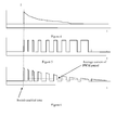
Figure 4 represents the evolution of in-rush current with time in the circuitry ofFigure 2 , -
Figure 5 represents the evolution of the modulation of the modulation circuitry, and -
Figure 6 represents the evolution of in-rush current with time in the circuitry ofFigure 4 . - The invention is based on a study of the appearance of the in-rush current, and more specifically the parameters which have an influence on this phenomenon.
-
Figure 2 is a schematic view of a basic implementation of a circuitry with a power switch. Thecircuitry 10 illustrated onFigure 1 comprises asupply pad 12 and thepower domain 14 which is always fed up with power. Bothsupply pad 12 andpower domain 14 are linked to aswitch 16. In the specific example ofFigure 1 ,supply pad 12 andpower domain 14 are in parallel with relation to switch 16.Such switch 16 enables to provide power from thesupply pad 12 and frompower domain 14 to thezone 18 to be provided with power. Therefore,switch 16 can be labeled a power switch.Switch 16 is enabled or disabled by a control circuit 19. - When
switch 16 is turned on, an in-rush current will flow fromsupply pad 12 as well as the always onpower domain 14. The evolution of such in-rush current with time is represented by the graph ofFigure 2 . The evolution is a decreasing exponential one with a peak current. Such peak current may be up to several A. 1A is considered for the value of peak current in the remainder of the description. - Such time evolution corresponds to the fact that the equivalent circuit of
circuitry 10 ofFigure 1 is a circuitry comprising a supply voltage submitted to a resistor and a capacitor placed in series. The capacitance of the equivalent capacitor can be deduced from the area of thezone 18 to be provided with power. The resistance of the equivalent resistor comes from theswitch 16 size. - In other words, the peak current can be deduced from the area of the
zone 18 to be provided with power, the supply voltage and theswitch 16 size. The evolution of the decreasing exponential is linked to the inverse of the product of the capacitance by the resistance. Thus, the time evolution is run by the area of thezone 18 to be provided with power and theswitch 16 size. - As the area of the
zone 18 to be provided with power and the supply voltage depend on thecircuitry 10 considered, it is suggested to modify theswitch 16 size, at least theswitch 16 size seen bycircuitry 10. - To achieve this, it is proposed the method to apply a modulation controlling the state of the
switch 16. By the expression "state", it should be understood that theswitch 16 has at least two states, a state wherezone 18 is provided with power and another state wherezone 18 is not provided with power. Such modulation modulates the equivalent resistance of theswitch 16 seen bycircuitry 10, so as to reduce the in-rush current created by switching onswitch 16 incircuitry 10. - A modulation of the state of
switch 16 enables to switch on and switch offswitch 16 alternatively. Therefore, compared to a case whereswitch 16 is only switched on once (for instance the case ofFigure 1 ), the modulation proposed enables to modulate the equivalence resistance ofswitch 16 seen bycircuitry 10. Indeed, whenswitch 16 is switched off, resistance ofswitch 16 seen bycircuitry 10 is equal to infinity. Thus, when considering a mean value, the resistance ofswitch 16 is increased compared to the case whereswitch 16 is only switched on. This results in a reduced in-rush current created by switching onswitch 16 incircuitry 10. This avoids the problem linked to a too large in-rush current. Notably, the always ondomain 14 will not get lower voltage and the risk of its failure decreases since the risk of not enough supply voltage is greatly reduced. - Such use may be implemented in
circuitry 10 represented onFigure 3 .Such circuitry 10 comprises the elements ofcircuitry 10 ofFigure 2 with acontrol circuit 20 substituted to the control circuit 19. Thecontrol circuit 20 is amodulation circuitry 20 comprising a modulation circuit 21 and adapted to control the state ofswitch 16 incircuitry 10 for modulating the equivalent resistance of the switch generated by the circuitry so as to reduce the in-rush current created by switching onswitch 16 incircuitry 10. - The size of the
modulation circuitry 20 is very reduced compared to the control circuitry of theswitch Figure 1 (prior art). Indeed, only digital circuitry is required. The use proposed therefore enables to reduce the in-rush current produced by a switch while limiting the extra area involved. - The modulation employed in
modulation circuitry 20 is preferably a modulation for which a duty cycle can be defined. In such case, the modulation can be divided in two states, an active state and an inactive state. The duty cycle is the ratio between the time spent by the modulation is in the active state and the total duration in time spent by the modulation is in both state (active and inactive). In other words, a low duty cycle (few percent for instance) corresponds to a low power because the modulation is mostly in the inactive state and a duty cycle of 100% corresponds to a case wherein the modulation is only in the active state. - The modulation employed in
modulation circuitry 20 is illustrated inFigure 5 . - A pulse-width modulation (also named after its acronym PWM) is an example of modulation for which a duty cycle can be defined. A pulse-width modulation is also named a pulse-duration modulation (also named after its acronym PDM). Pulse-width modulation, as illustrated in
Figure 5 , uses a rectangular pulse wave whose pulse width is modulated resulting in the variation of the average of the waveform. - The pulse-width of the first pulse, noted W1, is corresponding to a low percentage of the period of the signal. The pulse width of second pulse, noted W2, is corresponding is corresponding to a low percentage of the period of the signal so that W1 < W2. In a more general approach, pulse-widths are defined so that Wi < Wi+1, where i varies between 1 (first pulse) to n, pulse-width Wn corresponding to a duty cycle of 100%.
- Generating a pulse-width modulation can be made in a very easy way by the so-called "intersective method". According to this method, this can be carried out by using only sawtooth or a triangle waveform and a comparator. An oscillator is adapted to provide a sawtooth or a triangle waveform. In a more refined implementation, the characteristics of such pulse-width modulation are defined or optimized based on the equivalent capacitance and/or the equivalent resistance.
- In case the modulation for which a duty cycle can be defined, the first duty cycle W1 may be inferior to the duty cycle reached at a predetermined time Wt. This relation means that W1 < Wt Indeed, the equivalent resistance of
switch 16 seen bycircuitry 10 during the first duty cycle is then inferior to the equivalent resistance ofswitch 16 seen bycircuitry 10 at the predetermined time. This results in a reduced in-rush current. - Furthermore, the first duty cycle W1 may be inferior to 10% and the duty cycle reached at a predetermined time Wt may be superior to 80%. Indeed, with such values, the reduction obtained in the in-rush current is greatly enhanced. Mathematically both relations are fulfilled if W1 > 10% and Wt < 80%
- So as to enable a monotonic evolution of the equivalent resistance, the duty cycle increases with time. For instance, the duty cycle may increases from 1% to 100%, preferably from 10% to 100%.
- Moreover, the first period wherein the switch is in the on-state should be as short as possible. This enables to obtain a smooth evolution of the equivalent resistance of
switch 16 seen bycircuitry 10. As illustration, this first period lasts less than 100 ns, preferably less than 10 nanoseconds, more preferably less than 1 ns. -
Figure 6 represents the evolutions with time of in-rush current in thecircuitry 10 ofFigure 3 and according to the modulation applied by modulation circuitry 20 (seeFigure 5 ). The modulation corresponds to curve 22 whereas the in-rush current corresponds to curve 24. The modulation applied in this case is a PWM modulation whose duty cycle increases with time and represented inFigure 5 . When comparing the resulting in-rush current obtained in the case ofFigures 2 and 3 , the in-rush current is greatly reduced as expected. - In-rush current is now sliced in pulses whose width is corresponding to respective width pulse modulation. For example, a first modulation pulse (W1) with a duty cycle of 10% will lead to an in-rush current of 10% length. In summary, the method to apply a modulation enables the in-rush current to be cut, while the mean value of the in-rush current is lowered.
- In addition, according to the use illustrated by
Figure 6 , it appears that the in-rush current is tailored so as to reach a mean value different from 0 and represented as a dash line 26. This enables to obtain a substantially constant in-rush current which can be used for a dedicated purpose. Therefore, the mean value of the in-rush current may be determined based on a desired application. This can result in reduction in power consumption. For instance, mean values of the in-rush current may be equal to 100 mA or to 10 mA. - It is also proposed a
modulation circuitry 20 controlling the state of theswitch 16 incircuitry 10 for modulating the equivalent resistance ofswitch 16 seen bycircuitry 10 so as to reduce the in-rush current created by switching onswitch 16 incircuitry 10.Modulation circuitry 20 is adapted to produce a modulation for which a duty cycle is defined, the duty cycle increasing with time from 1% to 100%, preferably 10% to 100%.Such modulation circuitry 20 may be employed for controlling a switch and obtaining a reduced in-rush current with a limited area involved. - It is also proposed a set comprising
such modulation circuitry 20 and aswitch 16, theswitch 16 being controlled by themodulation circuitry 20. Such set may be included in a circuitry, the circuitry being for instance a circuitry adapted to be included in a mobile phone. - The invention has been described with reference to preferred embodiments. However, many variations are possible within the scope of the invention.
Claims (14)
- A method to apply a modulation controlling the state of a switch (16) in a circuitry (10) for modulating the equivalent resistance of the switch (16) seen by the circuitry (10), so as to reduce the in-rush current created by switching on the switch (16) in the circuitry (10).
- A method according to claim 1, wherein a duty cycle is defined for the modulation, the first duty cycle is inferior to the duty cycle reached at a predetermined time.
- A method according to claim 1 or claim 2, wherein a duty cycle is defined for the modulation, the first duty cycle is inferior to 10% and the duty cycle reached at a predetermined time is superior to 80%.
- A method according to any one of claims 1 to 3, wherein a duty cycle is defined for the modulation, the duty cycle is increasing with time.
- A method according to claim 4, wherein the duty cycle increases from 1% to 100%, preferably 10% to 100%.
- A method according to any one of claims 1 to 5, wherein an on-state is defined for the switch (16) and wherein during a first period, the switch (16) remains in the on-state for less than 100 ns, preferably less than 10 nanoseconds, more preferably less than 1 ns.
- A method according to any one of claims 1 to 6, wherein the in-rush current is tailored so as to reach a constant mean value different from 0.
- A method according to claim 7, wherein the mean value is determined based on the regime desired after application of the modulation.
- A method according to any one of claims 1 to 8, wherein the modulation is a pulse-width modulation.
- A modulation circuitry (20) controlling the state of a switch (16) in a circuitry (10) for modulating the equivalent resistance of the switch (16) seen by the circuitry (10) so as to reduce the in-rush current created by switching on the switch (16) in the circuitry (10), the modulation circuitry (20) being adapted to produce a modulation for which a duty cycle is defined, the duty cycle increasing with time from 1% to 100%, preferably 10% to 100%.
- A set comprising:- a switch (16),- a modulation circuitry (20) being adapted to control the state of the switch (16) in a circuitry (10) for modulating the equivalent resistance of the switch (16) seen by the circuitry (10) so as to reduce the in-rush current created by switching on the switch (16) in the circuitry (10).
- A set according to claim 11, wherein the modulation circuitry (20) is adapted to carry out the method to apply according to any one of claims 2 to 10.
- A circuitry comprising the set according to claim 11 or claim 12.
- A mobile phone comprising the circuitry according to claim 13.
Priority Applications (2)
| Application Number | Priority Date | Filing Date | Title |
|---|---|---|---|
| EP11306507.2A EP2595317A1 (en) | 2011-11-17 | 2011-11-17 | Method to apply a modulation controlling the state of a switch |
| PCT/EP2012/071228 WO2013072178A1 (en) | 2011-11-17 | 2012-10-26 | Method to apply a modulation controlling the state of a switch |
Applications Claiming Priority (1)
| Application Number | Priority Date | Filing Date | Title |
|---|---|---|---|
| EP11306507.2A EP2595317A1 (en) | 2011-11-17 | 2011-11-17 | Method to apply a modulation controlling the state of a switch |
Publications (1)
| Publication Number | Publication Date |
|---|---|
| EP2595317A1 true EP2595317A1 (en) | 2013-05-22 |
Family
ID=45217452
Family Applications (1)
| Application Number | Title | Priority Date | Filing Date |
|---|---|---|---|
| EP11306507.2A Withdrawn EP2595317A1 (en) | 2011-11-17 | 2011-11-17 | Method to apply a modulation controlling the state of a switch |
Country Status (2)
| Country | Link |
|---|---|
| EP (1) | EP2595317A1 (en) |
| WO (1) | WO2013072178A1 (en) |
Cited By (2)
| Publication number | Priority date | Publication date | Assignee | Title |
|---|---|---|---|---|
| GB2546961A (en) * | 2015-11-19 | 2017-08-09 | Continental automotive systems inc | High side output driver |
| CN118100618A (en) * | 2024-03-28 | 2024-05-28 | 西安视捷新能源有限公司 | A control method and device for solving light-load overvoltage of Vienna rectifier |
Citations (4)
| Publication number | Priority date | Publication date | Assignee | Title |
|---|---|---|---|---|
| US4625271A (en) * | 1984-10-05 | 1986-11-25 | Sundstrand Corporation | Soft-start circuit for a power converter |
| EP0532263A1 (en) * | 1991-09-13 | 1993-03-17 | Motorola, Inc. | DC/DC voltage converting device |
| US20070296386A1 (en) * | 2006-06-12 | 2007-12-27 | Nobuaki Umeki | Switching power-supply circuit and semiconductor integrated circuit |
| US20080185914A1 (en) * | 2007-02-05 | 2008-08-07 | Randall Anthony L | Redundant power supply with pulse width modulation soft start feature |
-
2011
- 2011-11-17 EP EP11306507.2A patent/EP2595317A1/en not_active Withdrawn
-
2012
- 2012-10-26 WO PCT/EP2012/071228 patent/WO2013072178A1/en not_active Ceased
Patent Citations (4)
| Publication number | Priority date | Publication date | Assignee | Title |
|---|---|---|---|---|
| US4625271A (en) * | 1984-10-05 | 1986-11-25 | Sundstrand Corporation | Soft-start circuit for a power converter |
| EP0532263A1 (en) * | 1991-09-13 | 1993-03-17 | Motorola, Inc. | DC/DC voltage converting device |
| US20070296386A1 (en) * | 2006-06-12 | 2007-12-27 | Nobuaki Umeki | Switching power-supply circuit and semiconductor integrated circuit |
| US20080185914A1 (en) * | 2007-02-05 | 2008-08-07 | Randall Anthony L | Redundant power supply with pulse width modulation soft start feature |
Cited By (3)
| Publication number | Priority date | Publication date | Assignee | Title |
|---|---|---|---|---|
| GB2546961A (en) * | 2015-11-19 | 2017-08-09 | Continental automotive systems inc | High side output driver |
| US10291012B2 (en) | 2015-11-19 | 2019-05-14 | Continental Powertrain USA, LLC | High side output driver |
| CN118100618A (en) * | 2024-03-28 | 2024-05-28 | 西安视捷新能源有限公司 | A control method and device for solving light-load overvoltage of Vienna rectifier |
Also Published As
| Publication number | Publication date |
|---|---|
| WO2013072178A1 (en) | 2013-05-23 |
Similar Documents
| Publication | Publication Date | Title |
|---|---|---|
| CN104410252B (en) | Source electrode drive circuit and its control method | |
| CN203416236U (en) | Gate driver for driving gate of switch, and system for switching high power load | |
| CN110958003B (en) | Adaptive gate driver | |
| EP1437823B1 (en) | Wide input range, DC-DC voltage-switching converter regulator device with boost and buck modes | |
| CN101277061A (en) | Synchronous Rectifier Control for Synchronous Boost Converter | |
| US8115523B2 (en) | Circuit to spread the spectrum of a PWM signal | |
| US20180342946A1 (en) | Active clamp power converter and method of reducing shoot-through current during soft start | |
| TW201251287A (en) | Constant on-time switching regulator implementing dual control loops | |
| US9531271B2 (en) | Spread spectrum power converter | |
| CN107749713B (en) | Load response improving unit, switching power converter and control method thereof | |
| CN102170282A (en) | Method and apparatus for adaptively modifying a pulse width of a pulse width modulated output | |
| JP7293342B2 (en) | Facilitating high-side control of switching power converters | |
| CN105449998A (en) | Circuit and method for driver control of switching circuit | |
| TW201014130A (en) | Level switch device for multilevel power converter | |
| CN104834340A (en) | Dynamic current pull-down for voltage regulator | |
| WO2015131595A1 (en) | Time-sequence control circuit and method | |
| EP2544371A1 (en) | Slew rate PWM controlled charge pump for limited in-rush current switch driving | |
| WO2013072178A1 (en) | Method to apply a modulation controlling the state of a switch | |
| US11843370B2 (en) | Switching device | |
| CN104682679B (en) | Power converter and its slope detection controller and method | |
| TW201117541A (en) | Dc-dc converter | |
| CN106448575B (en) | A backlight adjustment method and a backlight driving circuit | |
| CN101860180A (en) | MOS tube driver and power module | |
| AU2015377818B2 (en) | Electrical conversion | |
| US8134329B2 (en) | Buck converter with improved filter design |
Legal Events
| Date | Code | Title | Description |
|---|---|---|---|
| PUAI | Public reference made under article 153(3) epc to a published international application that has entered the european phase |
Free format text: ORIGINAL CODE: 0009012 |
|
| AK | Designated contracting states |
Kind code of ref document: A1 Designated state(s): AL AT BE BG CH CY CZ DE DK EE ES FI FR GB GR HR HU IE IS IT LI LT LU LV MC MK MT NL NO PL PT RO RS SE SI SK SM TR |
|
| AX | Request for extension of the european patent |
Extension state: BA ME |
|
| 17P | Request for examination filed |
Effective date: 20131030 |
|
| RBV | Designated contracting states (corrected) |
Designated state(s): AL AT BE BG CH CY CZ DE DK EE ES FI FR GB GR HR HU IE IS IT LI LT LU LV MC MK MT NL NO PL PT RO RS SE SI SK SM TR |
|
| RAP1 | Party data changed (applicant data changed or rights of an application transferred) |
Owner name: OCT CIRCUIT TECHNOLOGIES INTERNATIONAL LIMITED |
|
| STAA | Information on the status of an ep patent application or granted ep patent |
Free format text: STATUS: THE APPLICATION HAS BEEN WITHDRAWN |
|
| 18W | Application withdrawn |
Effective date: 20170703 |