EP2592650A1 - Silicon carbide substrate, semiconductor device, and soi wafer - Google Patents
Silicon carbide substrate, semiconductor device, and soi wafer Download PDFInfo
- Publication number
- EP2592650A1 EP2592650A1 EP11803571.6A EP11803571A EP2592650A1 EP 2592650 A1 EP2592650 A1 EP 2592650A1 EP 11803571 A EP11803571 A EP 11803571A EP 2592650 A1 EP2592650 A1 EP 2592650A1
- Authority
- EP
- European Patent Office
- Prior art keywords
- silicon carbide
- layer
- carbide substrate
- carbide layer
- thermal conductivity
- Prior art date
- Legal status (The legal status is an assumption and is not a legal conclusion. Google has not performed a legal analysis and makes no representation as to the accuracy of the status listed.)
- Granted
Links
Images

Classifications
-
- H—ELECTRICITY
- H10—SEMICONDUCTOR DEVICES; ELECTRIC SOLID-STATE DEVICES NOT OTHERWISE PROVIDED FOR
- H10D—INORGANIC ELECTRIC SEMICONDUCTOR DEVICES
- H10D86/00—Integrated devices formed in or on insulating or conducting substrates, e.g. formed in silicon-on-insulator [SOI] substrates or on stainless steel or glass substrates
-
- H—ELECTRICITY
- H10—SEMICONDUCTOR DEVICES; ELECTRIC SOLID-STATE DEVICES NOT OTHERWISE PROVIDED FOR
- H10D—INORGANIC ELECTRIC SEMICONDUCTOR DEVICES
- H10D62/00—Semiconductor bodies, or regions thereof, of devices having potential barriers
- H10D62/80—Semiconductor bodies, or regions thereof, of devices having potential barriers characterised by the materials
- H10D62/83—Semiconductor bodies, or regions thereof, of devices having potential barriers characterised by the materials being Group IV materials, e.g. B-doped Si or undoped Ge
- H10D62/832—Semiconductor bodies, or regions thereof, of devices having potential barriers characterised by the materials being Group IV materials, e.g. B-doped Si or undoped Ge being Group IV materials comprising two or more elements, e.g. SiGe
- H10D62/8325—Silicon carbide
-
- C—CHEMISTRY; METALLURGY
- C30—CRYSTAL GROWTH
- C30B—SINGLE-CRYSTAL GROWTH; UNIDIRECTIONAL SOLIDIFICATION OF EUTECTIC MATERIAL OR UNIDIRECTIONAL DEMIXING OF EUTECTOID MATERIAL; REFINING BY ZONE-MELTING OF MATERIAL; PRODUCTION OF A HOMOGENEOUS POLYCRYSTALLINE MATERIAL WITH DEFINED STRUCTURE; SINGLE CRYSTALS OR HOMOGENEOUS POLYCRYSTALLINE MATERIAL WITH DEFINED STRUCTURE; AFTER-TREATMENT OF SINGLE CRYSTALS OR A HOMOGENEOUS POLYCRYSTALLINE MATERIAL WITH DEFINED STRUCTURE; APPARATUS THEREFOR
- C30B29/00—Single crystals or homogeneous polycrystalline material with defined structure characterised by the material or by their shape
- C30B29/10—Inorganic compounds or compositions
- C30B29/36—Carbides
-
- H—ELECTRICITY
- H10—SEMICONDUCTOR DEVICES; ELECTRIC SOLID-STATE DEVICES NOT OTHERWISE PROVIDED FOR
- H10D—INORGANIC ELECTRIC SEMICONDUCTOR DEVICES
- H10D30/00—Field-effect transistors [FET]
- H10D30/60—Insulated-gate field-effect transistors [IGFET]
- H10D30/67—Thin-film transistors [TFT]
- H10D30/6758—Thin-film transistors [TFT] characterised by the insulating substrates
-
- H—ELECTRICITY
- H10—SEMICONDUCTOR DEVICES; ELECTRIC SOLID-STATE DEVICES NOT OTHERWISE PROVIDED FOR
- H10D—INORGANIC ELECTRIC SEMICONDUCTOR DEVICES
- H10D86/00—Integrated devices formed in or on insulating or conducting substrates, e.g. formed in silicon-on-insulator [SOI] substrates or on stainless steel or glass substrates
- H10D86/01—Manufacture or treatment
-
- H—ELECTRICITY
- H10—SEMICONDUCTOR DEVICES; ELECTRIC SOLID-STATE DEVICES NOT OTHERWISE PROVIDED FOR
- H10P—GENERIC PROCESSES OR APPARATUS FOR THE MANUFACTURE OR TREATMENT OF DEVICES COVERED BY CLASS H10
- H10P90/00—Preparation of wafers not covered by a single main group of this subclass, e.g. wafer reinforcement
- H10P90/19—Preparing inhomogeneous wafers
- H10P90/1904—Preparing vertically inhomogeneous wafers
- H10P90/1906—Preparing SOI wafers
-
- H—ELECTRICITY
- H10—SEMICONDUCTOR DEVICES; ELECTRIC SOLID-STATE DEVICES NOT OTHERWISE PROVIDED FOR
- H10W—GENERIC PACKAGES, INTERCONNECTIONS, CONNECTORS OR OTHER CONSTRUCTIONAL DETAILS OF DEVICES COVERED BY CLASS H10
- H10W10/00—Isolation regions in semiconductor bodies between components of integrated devices
- H10W10/10—Isolation regions comprising dielectric materials
- H10W10/181—Semiconductor-on-insulator [SOI] isolation regions, e.g. buried oxide regions of SOI wafers
-
- H—ELECTRICITY
- H10—SEMICONDUCTOR DEVICES; ELECTRIC SOLID-STATE DEVICES NOT OTHERWISE PROVIDED FOR
- H10W—GENERIC PACKAGES, INTERCONNECTIONS, CONNECTORS OR OTHER CONSTRUCTIONAL DETAILS OF DEVICES COVERED BY CLASS H10
- H10W40/00—Arrangements for thermal protection or thermal control
- H10W40/20—Arrangements for cooling
- H10W40/25—Arrangements for cooling characterised by their materials
- H10W40/255—Arrangements for cooling characterised by their materials having a laminate or multilayered structure, e.g. direct bond copper [DBC] ceramic substrates
-
- H—ELECTRICITY
- H10—SEMICONDUCTOR DEVICES; ELECTRIC SOLID-STATE DEVICES NOT OTHERWISE PROVIDED FOR
- H10W—GENERIC PACKAGES, INTERCONNECTIONS, CONNECTORS OR OTHER CONSTRUCTIONAL DETAILS OF DEVICES COVERED BY CLASS H10
- H10W70/00—Package substrates; Interposers; Redistribution layers [RDL]
- H10W70/60—Insulating or insulated package substrates; Interposers; Redistribution layers
- H10W70/67—Insulating or insulated package substrates; Interposers; Redistribution layers characterised by their insulating layers or insulating parts
- H10W70/69—Insulating materials thereof
- H10W70/692—Ceramics or glasses
Definitions
- the present invention relates to a silicon carbide substrate, a semiconductor device and an SOI wafer.
- the invention more particularly relates to a silicon carbide substrate for mounting a semiconductor element operating in a high-frequency region, and a semiconductor device and an SOI wafer using the same.
- Patent Literature 1 discloses a silicon carbide substrate composed of polycrystalline silicon carbide and having reduced loss in the high-frequency region by, for example, applying heat treatment.
- Patent Literature 1 JP 2009-260117A
- a semiconductor device having less high-frequency loss can be manufactured by mounting a semiconductor element on a surface of the silicon carbide substrate or forming an element using a silicon layer after its formation on the silicon carbide substrate through an insulating film.
- the silicon carbide substrate disclosed in Patent Literature 1 does not have a high thermal conductivity, sufficient heat dissipation may be hindered when a semiconductor element having a large amount of heat generation is mounted.
- the silicon carbide substrate disclosed in Patent Literature 1 is also known to have high insulation properties but does not have a high thermal conductivity as described above. Therefore, this silicon carbide substrate was not suitable in cases where excellent properties are required in both of the insulation properties and thermal conductivity.
- the present invention has been made to solve such prior art problems and has an object of providing a silicon carbide substrate having less high-frequency loss and exhibiting excellent heat dissipating characteristics. Another object of the invention is to provide a silicon carbide substrate exhibiting excellent insulation properties and heat dissipating characteristics. Still another object of the invention is to provide a semiconductor device and an SOI wafer which use such a silicon carbide substrate.
- a first silicon carbide substrate comprises: a first layer composed of polycrystalline silicon carbide; and a second layer composed of a polycrystalline silicon carbide and formed on a surface of the first layer, wherein the second layer has a less high-frequency loss than the first layer and the first layer has a higher thermal conductivity than the second layer.
- the high-frequency loss at a frequency of 20 GHz of the substrate is 2 dB/mm or less on a surface side of the second layer and the thermal conductivity of the substrate is 200 W/mK or more.
- the second layer preferably has a thickness of 10 ⁇ m or more accounting for up to 20% of a total thickness of the silicon carbide substrate.
- a second silicon carbide substrate comprises: a first layer composed of polycrystalline silicon carbide; and a second layer composed of polycrystalline silicon carbide and formed on a surface of the first layer, wherein the second layer has a higher specific resistance than the first layer and the first layer has a higher thermal conductivity than the second layer.
- the specific resistance of the substrate is 10 4 ⁇ cm or more on a surface side of the second layer and the thermal conductivity of the substrate is 200 W/mK or more.
- the first layer can be formed by a CVD process in an atmosphere containing nitrogen and the second layer can be formed by the CVD process in an atmosphere containing no nitrogen.
- a semiconductor device comprises the above-described silicon carbide substrate and a semiconductor element joined to a surface of the second layer of the silicon carbide substrate.
- An SOI wafer according to the invention comprises: the above-described silicon carbide substrate; an insulating layer formed on a surface of the second layer of the silicon carbide substrate; and a silicon layer formed on a surface of the insulating layer.
- a silicon carbide substrate obtained according to the invention includes a first layer and a second layer each composed of polycrystalline silicon carbide and has less high-frequency loss and exhibits excellent heat dissipating characteristics because the second layer has less high-frequency loss than the first layer and the first layer has a higher thermal conductivity than the second layer.
- a silicon carbide substrate S according to Embodiment 1 is shown in FIG. 1 .
- the silicon carbide substrate S is of a two-layer structure including a first silicon carbide layer 1 with a thickness D1 and a second silicon carbide layer 2 with a thickness D2 formed on a surface of the first silicon carbide layer 1.
- the first and second silicon carbide layers 1 and 2 are each composed of polycrystalline silicon carbide.
- the second silicon carbide layer 2 has less high-frequency loss than the first silicon carbide layer 1 and the first silicon carbide layer 1 has in the thickness direction a higher thermal conductivity than the second silicon carbide layer 2.
- the first silicon carbide layer 1 has a thermal conductivity of about 260 W/mK
- the second silicon carbide layer 2 has a thermal conductivity of about 100 W/mK.
- the first silicon carbide layer 1 has a value as large as about 50 dB/mm
- the second silicon carbide layer 2 has an extremely small value of about 1.4 to about 1.5 dB/mm.
- the second silicon carbide layer 2 has a specific resistance of 10 4 ⁇ cm or more.
- the silicon carbide substrate S By forming the two-layer structure including the first silicon carbide layer 1 and the second silicon carbide layer 2, the silicon carbide substrate S will have a high-frequency loss of 2 dB/mm or less at a frequency of 20 GHz on the surface side of the second silicon carbide layer 2 and a thermal conductivity of 200 W/mK or more in its thickness direction.
- the silicon carbide substrate S will also have a specific resistance of 10 4 ⁇ cm or more on the surface side of the second silicon carbide layer 2.
- the silicon carbide substrate S as described above can be fabricated as follows:
- the above-described formation method of the first silicon carbide layer 1 is repeated except that nitrogen gas is not supplied into the CVD apparatus, whereby silicon carbide is grown on the surfaces of the silicon carbide layer 1 to form the second silicon carbide layer 2.
- the surfaces of the thus formed second silicon carbide layer 2 are subjected to mechanical polishing using, for example, a diamond abrasive.
- the silicon carbide formed on the lateral surfaces of the graphite base material is ground and removed to obtain the graphite base material of which the upper surface and the lower surface each have the two-layer structure including the first silicon carbide layer 1 and the second silicon carbide layer 2 but the lateral surfaces are exposed.
- the graphite base material is heated in an oxygen atmosphere at a temperature of 900 to 1,400°C to burn and remove the graphite base material. Two silicon carbide substrates S are thus obtained.
- SiH 4 /CH 4 , SiH 4 /C 2 H 4 , SiH 4 /C 3 H 8 , SiCl 4 /CCl 4 , SiCl 4 /CH 4 , CH 3 SiCl 3 and (CH 3 ) 2 SiCl 2 may also be used as the material gases of silicon carbide.
- the first silicon carbide layer 1 was formed while supplying nitrogen gas and subsequently the second silicon carbide layer 2 was formed on the surfaces of the first silicon carbide layer 1 without supplying nitrogen gas.
- the formation of the first silicon carbide layer 1 and the formation of the second silicon carbide layer 2 may be performed consecutively while changing the conditions on the supply of nitrogen gas or be performed in separate steps independent of each other.
- a plurality of silicon carbide substrates S of the two-layer structure including the first silicon carbide layer 1 and the second silicon carbide layer 2 in which the total thickness Dt was fixed to 500 ⁇ m but the thickness D2 of the second silicon carbide layer 2 was changed to various values were fabricated and the high-frequency loss at a frequency of 20 GHz on the surface side of the second silicon carbide layer 2 was measured for each of the silicon carbide substrates S.
- the measurement results are shown in FIG. 2 . It is found that, when the thickness D2 of the second silicon carbide layer 2 is smaller than about 10 ⁇ m, the high-frequency loss value on the surface side of the second silicon carbide layer 2 increases sharply as the thickness D2 approaches 0. This is presumably because not only the second silicon carbide layer 2 as the surface layer but also the first silicon carbide layer 1 located on the lower side of the second silicon carbide layer 2 are affected by high-frequency waves due to the small thickness of the second silicon carbide layer 2.
- the thickness D2 of the second silicon carbide layer 2 is 10 ⁇ m or more, the high-frequency loss on the surface side of the second silicon carbide layer 2 has a value as small as up to 2 dB/mm and the high-frequency loss on the surface side of the second silicon carbide layer 2 is stable in a range of 1.4 to 1.5 dB/mm even if the thickness D2 has a large value which may approach 500 ⁇ m.
- a substrate showing a high-frequency loss of 2.0 dB/mm or less at a frequency of 20 GHz has no practical problem on the mounting of a semiconductor element operating in a high-frequency region. Therefore, the thickness D2 of the second silicon carbide layer 2 is preferably 10 ⁇ m or more.
- FIG. 3 shows a relation between the thickness D2 of the second silicon carbide layer 2 and the thermal conductivity of the whole of the silicon carbide substrate S in its thickness direction in the exemplary case where the thermal conductivity of the first silicon carbide layer 1 is 264 W/mK, that of the second silicon carbide layer 2 is about 105 W/mK and the total thickness Dt of the silicon carbide substrate S is 1,650 ⁇ m.
- the thermal conductivity of the whole of the silicon carbide substrate S increases with decreasing thickness D2 of the second silicon carbide layer 2.
- the inventors of the invention know that a sufficient heat-dissipating action may be achieved at a substrate thermal conductivity of 200 W/mK or more even when a semiconductor element operating in a high-frequency region is mounted.
- the thickness D2 of the second silicon carbide layer 2 corresponding to the thermal conductivity of 200 W/mK that is determined from the graph of FIG. 3 is about 350 ⁇ m, which shows that the thermal conductivity of the silicon carbide substrate S has a value of 200 W/mK or more when the thickness D2 of the second silicon carbide layer 2 is about 350 ⁇ m or less.
- the thickness D2 of about 350 ⁇ m is a value obtained with respect to the total thickness Dt of the silicon carbide substrate S of 1,650 ⁇ m, and the thickness D2 of the second silicon carbide layer 2 corresponding to the thermal conductivity of 200 W/mK varies with the total thickness Dt of the silicon carbide substrate S.
- the thermal conductivity of the silicon carbide substrate S is determined by the ratio of the thickness D2 of the second silicon carbide layer 2 to the total thickness Dt of the silicon carbide substrate S after the thermal conductivity of each of the first silicon carbide layer 1 and the second silicon carbide layer 2 is determined.
- the ratio of the thickness D2 of 350 ⁇ m to the total thickness Dt of 1,650 ⁇ m is about 20%.
- the thickness D2 of the second silicon carbide layer 2 is preferably up to 20% of the total thickness Dt of the silicon carbide substrate S.
- the thickness D2 of the second silicon carbide layer 2 is preferably set to a value of 10 ⁇ m or more which accounts for up to 20% of the total thickness Dt of the silicon carbide substrate S.
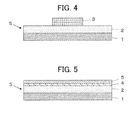
- the configuration of a semiconductor device according to Embodiment 2 is shown in FIG. 4 .
- the semiconductor device is the one having a semiconductor element 3 joined to a surface of the second silicon carbide layer 2 of the silicon carbide substrate S illustrated in Embodiment 1.
- the semiconductor element 3 is joined to the surface of the second silicon carbide layer 2 by, for example, brazing. It is also possible to form a predetermined conductive pattern on the surface of the second silicon carbide layer 2 and join the semiconductor element 3 onto the conductive pattern using a solder.
- the silicon carbide substrate S has a high-frequency loss as small as up to 2 dB/mm at a frequency of 20 GHz on the side of the surface of the second silicon carbide layer 2 on which the semiconductor element 3 is to be mounted, and also has a thermal conductivity of 200 W/mK or more, and therefore enables a highly reliable and stable operation to be performed even when the semiconductor element 3 is an element operating in a high-frequency region.
- the silicon carbide substrate S has a specific resistance as high as at least 10 4 ⁇ cm on the surface side of the second silicon carbide layer 2, the stable operation is ensured even when the semiconductor element 3 is used to configure a circuit requiring excellent insulation properties.
- FIG. 5 The configuration of an SOI (Silicon on Insulator) wafer according to Embodiment 3 is shown in FIG. 5 .
- the SOI wafer is obtained by forming an insulating layer 4 composed of SiO 2 or the like on a surface of the second silicon carbide layer 2 of the silicon carbide substrate S illustrated in Embodiment 1 and forming a silicon layer 5 on a surface of the insulating layer 4.
- the silicon layer 5 is used to form circuit components.
- the silicon carbide substrate S has a high-frequency loss as small as up to 2 dB/mm at a frequency of 20 GHz on the surface side of the second silicon carbide layer 2 and also has a thermal conductivity of 200 W/mK or more, and therefore an apparatus capable of a highly reliable and stable operation is realized even when the silicon layer 5 is used to form an element operating in a high-frequency region.
- the silicon carbide substrate S has a specific resistance as high as at least 10 4 ⁇ cm on the surface side of the second silicon carbide layer 2, the highly reliable and stable operation is possible even when the silicon layer 5 is used to configure a circuit requiring excellent insulation properties.
- a high-frequency circuit board for processing microwave, millimeter-wave or other signals may also be fabricated by forming high-frequency transmission lines on the silicon carbide substrate S illustrated in Embodiment 1.
- the presence of the silicon carbide substrate S enables a high-frequency circuit board having reduced transmission loss of high-frequency signals to be obtained.
Landscapes
- Chemical & Material Sciences (AREA)
- Inorganic Chemistry (AREA)
- Engineering & Computer Science (AREA)
- Crystallography & Structural Chemistry (AREA)
- Materials Engineering (AREA)
- Metallurgy (AREA)
- Organic Chemistry (AREA)
- Cooling Or The Like Of Semiconductors Or Solid State Devices (AREA)
- Recrystallisation Techniques (AREA)
- Electrodes Of Semiconductors (AREA)
Abstract
Description
- The present invention relates to a silicon carbide substrate, a semiconductor device and an SOI wafer. The invention more particularly relates to a silicon carbide substrate for mounting a semiconductor element operating in a high-frequency region, and a semiconductor device and an SOI wafer using the same.
- Semiconductor elements operating in the high-frequency region are conventionally used in electronic devices including mobile phones and various communication equipments and various dielectric ceramics have been proposed as the substrate materials for mounting such semiconductor elements.
Of those dielectric ceramics, silicon carbide is particularly known to have high mechanical strength and stable chemical properties in combination. However, because of the large loss in the high-frequency region, silicon carbide that was used in conventional mechanical parts and the like was not suitable for the material of a substrate on which a high-frequency semiconductor element is to be mounted.
Then, for instance,Patent Literature 1 discloses a silicon carbide substrate composed of polycrystalline silicon carbide and having reduced loss in the high-frequency region by, for example, applying heat treatment. - Patent Literature 1:
JP 2009-260117A - With the use of such a silicon carbide substrate, a semiconductor device having less high-frequency loss can be manufactured by mounting a semiconductor element on a surface of the silicon carbide substrate or forming an element using a silicon layer after its formation on the silicon carbide substrate through an insulating film.
However, since the silicon carbide substrate disclosed inPatent Literature 1 does not have a high thermal conductivity, sufficient heat dissipation may be hindered when a semiconductor element having a large amount of heat generation is mounted.
The silicon carbide substrate disclosed inPatent Literature 1 is also known to have high insulation properties but does not have a high thermal conductivity as described above. Therefore, this silicon carbide substrate was not suitable in cases where excellent properties are required in both of the insulation properties and thermal conductivity. - The present invention has been made to solve such prior art problems and has an object of providing a silicon carbide substrate having less high-frequency loss and exhibiting excellent heat dissipating characteristics.
Another object of the invention is to provide a silicon carbide substrate exhibiting excellent insulation properties and heat dissipating characteristics.
Still another object of the invention is to provide a semiconductor device and an SOI wafer which use such a silicon carbide substrate. - A first silicon carbide substrate according to the invention comprises: a first layer composed of polycrystalline silicon carbide; and a second layer composed of a polycrystalline silicon carbide and formed on a surface of the first layer, wherein the second layer has a less high-frequency loss than the first layer and the first layer has a higher thermal conductivity than the second layer.
Preferably, the high-frequency loss at a frequency of 20 GHz of the substrate is 2 dB/mm or less on a surface side of the second layer and the thermal conductivity of the substrate is 200 W/mK or more.
The second layer preferably has a thickness of 10 µm or more accounting for up to 20% of a total thickness of the silicon carbide substrate.
A second silicon carbide substrate according to the invention comprises: a first layer composed of polycrystalline silicon carbide; and a second layer composed of polycrystalline silicon carbide and formed on a surface of the first layer, wherein the second layer has a higher specific resistance than the first layer and the first layer has a higher thermal conductivity than the second layer.
Preferably, the specific resistance of the substrate is 104 Ωcm or more on a surface side of the second layer and the thermal conductivity of the substrate is 200 W/mK or more.
In each of the first and second silicon carbide substrates, the first layer can be formed by a CVD process in an atmosphere containing nitrogen and the second layer can be formed by the CVD process in an atmosphere containing no nitrogen. - A semiconductor device according to the invention comprises the above-described silicon carbide substrate and a semiconductor element joined to a surface of the second layer of the silicon carbide substrate.
An SOI wafer according to the invention comprises: the above-described silicon carbide substrate; an insulating layer formed on a surface of the second layer of the silicon carbide substrate; and a silicon layer formed on a surface of the insulating layer. - A silicon carbide substrate obtained according to the invention includes a first layer and a second layer each composed of polycrystalline silicon carbide and has less high-frequency loss and exhibits excellent heat dissipating characteristics because the second layer has less high-frequency loss than the first layer and the first layer has a higher thermal conductivity than the second layer.
-
- [
FIG. 1] FIG. 1 is a cross-sectional view showing a silicon carbide substrate according toEmbodiment 1 of the invention. - [
FIG. 2] FIG. 2 is a graph showing the relation between the thickness of a second silicon carbide layer and the high-frequency loss of the whole of the silicon carbide substrate. - [
FIG. 3] FIG. 3 is a graph showing the relation between the thickness of the second silicon carbide layer and the thermal conductivity of the whole of the silicon carbide substrate. - [
FIG. 4] FIG. 4 is a cross-sectional view showing a semiconductor device according toEmbodiment 2. - [
FIG. 5] FIG. 5 is a cross-sectional view showing an SOI wafer according toEmbodiment 3. - Embodiments of the invention are described below with reference to the accompanying drawings.
- A silicon carbide substrate S according to
Embodiment 1 is shown inFIG. 1 . The silicon carbide substrate S is of a two-layer structure including a firstsilicon carbide layer 1 with a thickness D1 and a secondsilicon carbide layer 2 with a thickness D2 formed on a surface of the firstsilicon carbide layer 1. The first and secondsilicon carbide layers silicon carbide layer 2 has less high-frequency loss than the firstsilicon carbide layer 1 and the firstsilicon carbide layer 1 has in the thickness direction a higher thermal conductivity than the secondsilicon carbide layer 2. - For example, the first
silicon carbide layer 1 has a thermal conductivity of about 260 W/mK, whereas the secondsilicon carbide layer 2 has a thermal conductivity of about 100 W/mK.
With regard to the high-frequency loss at a frequency of 20 GHz, the firstsilicon carbide layer 1 has a value as large as about 50 dB/mm, whereas the secondsilicon carbide layer 2 has an extremely small value of about 1.4 to about 1.5 dB/mm.
In addition, the secondsilicon carbide layer 2 has a specific resistance of 104 Ωcm or more.
By forming the two-layer structure including the firstsilicon carbide layer 1 and the secondsilicon carbide layer 2, the silicon carbide substrate S will have a high-frequency loss of 2 dB/mm or less at a frequency of 20 GHz on the surface side of the secondsilicon carbide layer 2 and a thermal conductivity of 200 W/mK or more in its thickness direction. The silicon carbide substrate S will also have a specific resistance of 104 Ωcm or more on the surface side of the secondsilicon carbide layer 2. - The silicon carbide substrate S as described above can be fabricated as follows:
- First, a graphite base material is held in a CVD apparatus, the internal pressure of the CVD apparatus is adjusted to, for example, 1.3 kPa and silicon carbide material gases including SiCl4 and C3H8 are supplied into the CVD apparatus at a volume ratio of 5 to 20% together with hydrogen gas serving as a carrier gas. Nitrogen gas is further supplied at a volume ratio of 0.5 to 2.5% with respect to the material gases and heating to a temperature of, for example, 1,000 to 1,600°C is carried out to grow silicon carbide to a predetermined thickness on the upper surface, lower surface and lateral surfaces of the graphite base material. The silicon carbide forms the first
silicon carbide layer 1. - Next, after the CVD apparatus is once evacuated, the above-described formation method of the first
silicon carbide layer 1 is repeated except that nitrogen gas is not supplied into the CVD apparatus, whereby silicon carbide is grown on the surfaces of thesilicon carbide layer 1 to form the secondsilicon carbide layer 2. - The surfaces of the thus formed second
silicon carbide layer 2 are subjected to mechanical polishing using, for example, a diamond abrasive. After that, the silicon carbide formed on the lateral surfaces of the graphite base material is ground and removed to obtain the graphite base material of which the upper surface and the lower surface each have the two-layer structure including the firstsilicon carbide layer 1 and the secondsilicon carbide layer 2 but the lateral surfaces are exposed.
Then, the graphite base material is heated in an oxygen atmosphere at a temperature of 900 to 1,400°C to burn and remove the graphite base material. Two silicon carbide substrates S are thus obtained. - SiH4/CH4, SiH4/C2H4, SiH4/C3H8, SiCl4/CCl4, SiCl4/CH4, CH3SiCl3 and (CH3)2SiCl2 may also be used as the material gases of silicon carbide.
In the above-described method, the firstsilicon carbide layer 1 was formed while supplying nitrogen gas and subsequently the secondsilicon carbide layer 2 was formed on the surfaces of the firstsilicon carbide layer 1 without supplying nitrogen gas. However, contrary to the above, it is also possible to first form the secondsilicon carbide layer 2 under the condition that nitrogen gas is not supplied and subsequently form the firstsilicon carbide layer 1 on the surfaces of the secondsilicon carbide layer 2 while supplying nitrogen gas.
The formation of the firstsilicon carbide layer 1 and the formation of the secondsilicon carbide layer 2 may be performed consecutively while changing the conditions on the supply of nitrogen gas or be performed in separate steps independent of each other. - A plurality of silicon carbide substrates S of the two-layer structure including the first
silicon carbide layer 1 and the secondsilicon carbide layer 2 in which the total thickness Dt was fixed to 500 µm but the thickness D2 of the secondsilicon carbide layer 2 was changed to various values were fabricated and the high-frequency loss at a frequency of 20 GHz on the surface side of the secondsilicon carbide layer 2 was measured for each of the silicon carbide substrates S. The measurement results are shown inFIG. 2 .
It is found that, when the thickness D2 of the secondsilicon carbide layer 2 is smaller than about 10 µm, the high-frequency loss value on the surface side of the secondsilicon carbide layer 2 increases sharply as the thickness D2 approaches 0. This is presumably because not only the secondsilicon carbide layer 2 as the surface layer but also the firstsilicon carbide layer 1 located on the lower side of the secondsilicon carbide layer 2 are affected by high-frequency waves due to the small thickness of the secondsilicon carbide layer 2. - On the other hand, when the thickness D2 of the second
silicon carbide layer 2 is 10 µm or more, the high-frequency loss on the surface side of the secondsilicon carbide layer 2 has a value as small as up to 2 dB/mm and the high-frequency loss on the surface side of the secondsilicon carbide layer 2 is stable in a range of 1.4 to 1.5 dB/mm even if the thickness D2 has a large value which may approach 500 µm.
According to the findings of the present inventors, a substrate showing a high-frequency loss of 2.0 dB/mm or less at a frequency of 20 GHz has no practical problem on the mounting of a semiconductor element operating in a high-frequency region. Therefore, the thickness D2 of the secondsilicon carbide layer 2 is preferably 10 µm or more. -
FIG. 3 shows a relation between the thickness D2 of the secondsilicon carbide layer 2 and the thermal conductivity of the whole of the silicon carbide substrate S in its thickness direction in the exemplary case where the thermal conductivity of the firstsilicon carbide layer 1 is 264 W/mK, that of the secondsilicon carbide layer 2 is about 105 W/mK and the total thickness Dt of the silicon carbide substrate S is 1,650 µm.
The thermal conductivity of the whole of the silicon carbide substrate S increases with decreasing thickness D2 of the secondsilicon carbide layer 2.
The inventors of the invention know that a sufficient heat-dissipating action may be achieved at a substrate thermal conductivity of 200 W/mK or more even when a semiconductor element operating in a high-frequency region is mounted. - The thickness D2 of the second
silicon carbide layer 2 corresponding to the thermal conductivity of 200 W/mK that is determined from the graph ofFIG. 3 is about 350 µm, which shows that the thermal conductivity of the silicon carbide substrate S has a value of 200 W/mK or more when the thickness D2 of the secondsilicon carbide layer 2 is about 350 µm or less. However, the thickness D2 of about 350 µm is a value obtained with respect to the total thickness Dt of the silicon carbide substrate S of 1,650 µm, and the thickness D2 of the secondsilicon carbide layer 2 corresponding to the thermal conductivity of 200 W/mK varies with the total thickness Dt of the silicon carbide substrate S. It seems that the thermal conductivity of the silicon carbide substrate S is determined by the ratio of the thickness D2 of the secondsilicon carbide layer 2 to the total thickness Dt of the silicon carbide substrate S after the thermal conductivity of each of the firstsilicon carbide layer 1 and the secondsilicon carbide layer 2 is determined. The ratio of the thickness D2 of 350 µm to the total thickness Dt of 1,650 µm is about 20%. - Therefore, in order that the silicon carbide substrate S may have a thermal conductivity of 200 W/mK or more, the thickness D2 of the second
silicon carbide layer 2 is preferably up to 20% of the total thickness Dt of the silicon carbide substrate S.
In other words, in consideration of both of the high-frequency loss and the heat dissipating characteristics, the thickness D2 of the secondsilicon carbide layer 2 is preferably set to a value of 10 µm or more which accounts for up to 20% of the total thickness Dt of the silicon carbide substrate S. - The configuration of a semiconductor device according to
Embodiment 2 is shown inFIG. 4 . The semiconductor device is the one having asemiconductor element 3 joined to a surface of the secondsilicon carbide layer 2 of the silicon carbide substrate S illustrated inEmbodiment 1. Thesemiconductor element 3 is joined to the surface of the secondsilicon carbide layer 2 by, for example, brazing.
It is also possible to form a predetermined conductive pattern on the surface of the secondsilicon carbide layer 2 and join thesemiconductor element 3 onto the conductive pattern using a solder.
According to the thus configured semiconductor device, the silicon carbide substrate S has a high-frequency loss as small as up to 2 dB/mm at a frequency of 20 GHz on the side of the surface of the secondsilicon carbide layer 2 on which thesemiconductor element 3 is to be mounted, and also has a thermal conductivity of 200 W/mK or more, and therefore enables a highly reliable and stable operation to be performed even when thesemiconductor element 3 is an element operating in a high-frequency region.
In addition, since the silicon carbide substrate S has a specific resistance as high as at least 104 Ωcm on the surface side of the secondsilicon carbide layer 2, the stable operation is ensured even when thesemiconductor element 3 is used to configure a circuit requiring excellent insulation properties. - The configuration of an SOI (Silicon on Insulator) wafer according to
Embodiment 3 is shown inFIG. 5 . The SOI wafer is obtained by forming an insulating layer 4 composed of SiO2 or the like on a surface of the secondsilicon carbide layer 2 of the silicon carbide substrate S illustrated inEmbodiment 1 and forming asilicon layer 5 on a surface of the insulating layer 4. Thesilicon layer 5 is used to form circuit components.
Also in the SOI wafer, the silicon carbide substrate S has a high-frequency loss as small as up to 2 dB/mm at a frequency of 20 GHz on the surface side of the secondsilicon carbide layer 2 and also has a thermal conductivity of 200 W/mK or more, and therefore an apparatus capable of a highly reliable and stable operation is realized even when thesilicon layer 5 is used to form an element operating in a high-frequency region.
In addition, since the silicon carbide substrate S has a specific resistance as high as at least 104 Ωcm on the surface side of the secondsilicon carbide layer 2, the highly reliable and stable operation is possible even when thesilicon layer 5 is used to configure a circuit requiring excellent insulation properties. - In addition, a high-frequency circuit board for processing microwave, millimeter-wave or other signals may also be fabricated by forming high-frequency transmission lines on the silicon carbide substrate S illustrated in
Embodiment 1. The presence of the silicon carbide substrate S enables a high-frequency circuit board having reduced transmission loss of high-frequency signals to be obtained. - 1 first silicon carbide layer, 2 second silicon carbide layer, 3 semiconductor element, 4 insulating layer, 5 silicon layer, S silicon carbide substrate.
Claims (8)
- A silicon carbide substrate comprising:a first layer composed of polycrystalline silicon carbide; anda second layer composed of polycrystalline silicon carbide and formed on a surface of said first layer,wherein said second layer has a less high-frequency loss than said first layer and said first layer has a higher thermal conductivity than said second layer.
- The silicon carbide substrate according to claim 1, whose high-frequency loss at a frequency of 20 GHz is 2 dB/mm or less on a surface side of said second layer and whose thermal conductivity is 200 W/mK or more.
- The silicon carbide substrate according to claim 1 or 2, wherein said-second layer has a thickness of 10 µm or more accounting for up to 20% of a total thickness of said silicon carbide substrate.
- A silicon carbide substrate comprising:a first layer composed of polycrystalline silicon carbide; anda second layer composed of polycrystalline silicon carbide and formed on a surface of said first layer,wherein said second layer has a higher specific resistance than said first layer and said first layer has a higher thermal conductivity than said second layer.
- The silicon carbide substrate according to claim 4, whose specific resistance is 104 Ωcm or more on a surface side of said second layer and whose thermal conductivity is 200 W/mK or more.
- The silicon carbide substrate according to any one of claims 1 to 5, wherein said first layer is formed by a chemical vapor deposition process in an atmosphere containing nitrogen and said second layer is formed by the chemical vapor deposition process in an atmosphere containing no nitrogen.
- A semiconductor device comprising:the silicon carbide substrate according to any one of claims 1 to 6; anda semiconductor element joined to a surface of said second layer of said silicon carbide substrate.
- An SOI wafer comprising:the silicon carbide substrate according to any one of claims 1 to 6;an insulating layer formed on a surface of said second layer of said silicon carbide substrate; anda silicon layer formed on a surface of said insulating layer.
Applications Claiming Priority (2)
| Application Number | Priority Date | Filing Date | Title |
|---|---|---|---|
| JP2010153730A JP4956649B2 (en) | 2010-07-06 | 2010-07-06 | Silicon carbide substrate, semiconductor device and SOI wafer |
| PCT/JP2011/065342 WO2012005237A1 (en) | 2010-07-06 | 2011-07-05 | Silicon carbide substrate, semiconductor device, and soi wafer |
Publications (3)
| Publication Number | Publication Date |
|---|---|
| EP2592650A1 true EP2592650A1 (en) | 2013-05-15 |
| EP2592650A4 EP2592650A4 (en) | 2015-04-01 |
| EP2592650B1 EP2592650B1 (en) | 2016-09-07 |
Family
ID=45441216
Family Applications (1)
| Application Number | Title | Priority Date | Filing Date |
|---|---|---|---|
| EP11803571.6A Active EP2592650B1 (en) | 2010-07-06 | 2011-07-05 | Silicon carbide substrate, semiconductor device, and soi wafer |
Country Status (7)
| Country | Link |
|---|---|
| US (1) | US8507922B2 (en) |
| EP (1) | EP2592650B1 (en) |
| JP (1) | JP4956649B2 (en) |
| KR (1) | KR101261898B1 (en) |
| CN (1) | CN103003937A (en) |
| TW (1) | TWI536558B (en) |
| WO (1) | WO2012005237A1 (en) |
Families Citing this family (11)
| Publication number | Priority date | Publication date | Assignee | Title |
|---|---|---|---|---|
| FR2953640B1 (en) * | 2009-12-04 | 2012-02-10 | S O I Tec Silicon On Insulator Tech | METHOD FOR MANUFACTURING A SEMICONDUCTOR TYPE STRUCTURE ON INSULATION, WITH REDUCED ELECTRICAL LOSSES AND CORRESPONDING STRUCTURE |
| JP2016092122A (en) * | 2014-10-31 | 2016-05-23 | 三井造船株式会社 | Silicon carbide substrate |
| KR20170019676A (en) * | 2015-08-12 | 2017-02-22 | 삼성전자주식회사 | Fabricating method of a semiconductor device |
| JP6533451B2 (en) * | 2015-11-09 | 2019-06-19 | 住友電気工業株式会社 | Wireless power receiver |
| KR102051668B1 (en) * | 2016-12-20 | 2019-12-04 | 주식회사 티씨케이 | A PART FOR SEMICONDUCTOR MANUFACTORING WITH SiC DEPOSITION LAYER AND MANUFACTORING METHOD THE SAME |
| JP2018157165A (en) | 2017-03-21 | 2018-10-04 | 株式会社東芝 | Semiconductor device, inverter circuit, drive device, vehicle, and elevator |
| US10600635B2 (en) | 2017-04-20 | 2020-03-24 | Elyakim Kassel | Method and apparatus for a semiconductor-on-higher thermal conductive multi-layer composite wafer |
| JP7322371B2 (en) * | 2018-09-27 | 2023-08-08 | 住友金属鉱山株式会社 | Method for manufacturing polycrystalline silicon carbide substrate |
| US11942534B2 (en) | 2022-03-08 | 2024-03-26 | Globalfoundries U.S. Inc. | Bipolar transistor with thermal conductor |
| FR3150342B1 (en) | 2023-06-26 | 2025-06-27 | Soitec Silicon On Insulator | POLYCRYSTALLINE SILICON CARBIDE SUPPORT FOR A SUBSTRATE INTENDED TO RECEIVE POWER SEMICONDUCTOR DEVICES AND SUBSTRATE COMPRISING SUCH A SUPPORT. |
| CN119725233B (en) * | 2025-02-27 | 2025-06-20 | 山东大学 | Silicon carbide insulating substrate based on double-sided aluminum coating and preparation method thereof |
Family Cites Families (7)
| Publication number | Priority date | Publication date | Assignee | Title |
|---|---|---|---|---|
| FR2781082B1 (en) * | 1998-07-10 | 2002-09-20 | Commissariat Energie Atomique | SEMICONDUCTOR THIN-LAYER STRUCTURE HAVING A HEAT-DISTRIBUTING LAYER |
| US20020089016A1 (en) * | 1998-07-10 | 2002-07-11 | Jean-Pierre Joly | Thin layer semi-conductor structure comprising a heat distribution layer |
| EP1358681A4 (en) * | 2001-01-03 | 2008-04-30 | Univ Mississippi | SILICON CARBIDE AND RELATED TRANSISTORS WITH A WIDE ENERGY DIFFERENCE FOR SEMI-INSULATING EPITAXIC LAYER FOR USE IN HIGH SPEED AND HIGH POWER APPLICATIONS |
| JP3881562B2 (en) * | 2002-02-22 | 2007-02-14 | 三井造船株式会社 | SiC monitor wafer manufacturing method |
| US20050070048A1 (en) * | 2003-09-25 | 2005-03-31 | Tolchinsky Peter G. | Devices and methods employing high thermal conductivity heat dissipation substrates |
| US7361930B2 (en) * | 2005-03-21 | 2008-04-22 | Agilent Technologies, Inc. | Method for forming a multiple layer passivation film and a device incorporating the same |
| JP5260127B2 (en) * | 2008-04-18 | 2013-08-14 | 国立大学法人東北大学 | Method for producing silicon carbide |
-
2010
- 2010-07-06 JP JP2010153730A patent/JP4956649B2/en active Active
-
2011
- 2011-06-30 TW TW100123088A patent/TWI536558B/en active
- 2011-07-05 WO PCT/JP2011/065342 patent/WO2012005237A1/en not_active Ceased
- 2011-07-05 US US13/808,556 patent/US8507922B2/en active Active
- 2011-07-05 KR KR1020127033927A patent/KR101261898B1/en active Active
- 2011-07-05 CN CN2011800323572A patent/CN103003937A/en active Pending
- 2011-07-05 EP EP11803571.6A patent/EP2592650B1/en active Active
Also Published As
| Publication number | Publication date |
|---|---|
| TWI536558B (en) | 2016-06-01 |
| EP2592650A4 (en) | 2015-04-01 |
| CN103003937A (en) | 2013-03-27 |
| KR20130018338A (en) | 2013-02-20 |
| TW201212225A (en) | 2012-03-16 |
| JP2012018960A (en) | 2012-01-26 |
| KR101261898B1 (en) | 2013-05-07 |
| EP2592650B1 (en) | 2016-09-07 |
| US8507922B2 (en) | 2013-08-13 |
| WO2012005237A1 (en) | 2012-01-12 |
| JP4956649B2 (en) | 2012-06-20 |
| US20130112997A1 (en) | 2013-05-09 |
Similar Documents
| Publication | Publication Date | Title |
|---|---|---|
| EP2592650B1 (en) | Silicon carbide substrate, semiconductor device, and soi wafer | |
| KR102180947B1 (en) | Selective deposition of diamond in thermal vias | |
| Huang et al. | Antennas in glass interposer for sub-THz applications | |
| EP4015486B1 (en) | Ceramic substrate, circuit board and method for producing same, and power module | |
| KR102652250B1 (en) | Substrate for integrated radio frequency device and method for manufacturing same | |
| JP2019527925A5 (en) | ||
| CN109791911A (en) | The production method of substrate-placing platform and substrate-placing platform | |
| US8465719B2 (en) | Silicon carbide substrate, semiconductor device, wiring substrate, and silicon carbide manufacturing method | |
| US11476178B2 (en) | Selectively-pliable chemical vapor deposition (CVD) diamond or other heat spreader | |
| CN113571416B (en) | A diamond-based gallium nitride high electron mobility transistor and its preparation method | |
| CN104465453B (en) | The wafer heater of plasma CVD equipment | |
| JP2016092122A (en) | Silicon carbide substrate | |
| He et al. | RF characterization of coplanar waveguide (CPW) transmission lines on single-crystalline diamond platform for integrated high power RF electronic systems | |
| US10600635B2 (en) | Method and apparatus for a semiconductor-on-higher thermal conductive multi-layer composite wafer | |
| EP4485502A1 (en) | Radio-frequency device substrate, and method for manufacturing same | |
| JP7334869B2 (en) | Nitride semiconductor substrate and manufacturing method thereof | |
| US20200067161A1 (en) | High-frequency substrate and manufacturing method for high-performance, high-frequency applications | |
| KR20120140495A (en) | Electrode for plasma generation and method of manufacturing the same | |
| TWI223337B (en) | Method of gap filling with high density plasma chemical vapor deposition | |
| JPS60167358A (en) | Circuit board for loading semiconductor element | |
| JPH0610139A (en) | Thin film deposition device |
Legal Events
| Date | Code | Title | Description |
|---|---|---|---|
| PUAI | Public reference made under article 153(3) epc to a published international application that has entered the european phase |
Free format text: ORIGINAL CODE: 0009012 |
|
| 17P | Request for examination filed |
Effective date: 20130104 |
|
| AK | Designated contracting states |
Kind code of ref document: A1 Designated state(s): AL AT BE BG CH CY CZ DE DK EE ES FI FR GB GR HR HU IE IS IT LI LT LU LV MC MK MT NL NO PL PT RO RS SE SI SK SM TR |
|
| DAX | Request for extension of the european patent (deleted) | ||
| RA4 | Supplementary search report drawn up and despatched (corrected) |
Effective date: 20150303 |
|
| RIC1 | Information provided on ipc code assigned before grant |
Ipc: C30B 29/36 20060101ALI20150225BHEP Ipc: H01L 23/15 20060101AFI20150225BHEP Ipc: H01L 27/12 20060101ALI20150225BHEP |
|
| REG | Reference to a national code |
Ref country code: DE Ref legal event code: R079 Ref document number: 602011030216 Country of ref document: DE Free format text: PREVIOUS MAIN CLASS: H01L0023150000 Ipc: H01L0023373000 |
|
| GRAP | Despatch of communication of intention to grant a patent |
Free format text: ORIGINAL CODE: EPIDOSNIGR1 |
|
| RIC1 | Information provided on ipc code assigned before grant |
Ipc: H01L 23/373 20060101AFI20160126BHEP |
|
| INTG | Intention to grant announced |
Effective date: 20160303 |
|
| GRAS | Grant fee paid |
Free format text: ORIGINAL CODE: EPIDOSNIGR3 |
|
| GRAA | (expected) grant |
Free format text: ORIGINAL CODE: 0009210 |
|
| AK | Designated contracting states |
Kind code of ref document: B1 Designated state(s): AL AT BE BG CH CY CZ DE DK EE ES FI FR GB GR HR HU IE IS IT LI LT LU LV MC MK MT NL NO PL PT RO RS SE SI SK SM TR |
|
| REG | Reference to a national code |
Ref country code: GB Ref legal event code: FG4D |
|
| REG | Reference to a national code |
Ref country code: CH Ref legal event code: EP |
|
| REG | Reference to a national code |
Ref country code: IE Ref legal event code: FG4D |
|
| REG | Reference to a national code |
Ref country code: AT Ref legal event code: REF Ref document number: 827534 Country of ref document: AT Kind code of ref document: T Effective date: 20161015 |
|
| REG | Reference to a national code |
Ref country code: DE Ref legal event code: R096 Ref document number: 602011030216 Country of ref document: DE |
|
| REG | Reference to a national code |
Ref country code: SE Ref legal event code: TRGR |
|
| REG | Reference to a national code |
Ref country code: LT Ref legal event code: MG4D |
|
| REG | Reference to a national code |
Ref country code: NL Ref legal event code: MP Effective date: 20160907 |
|
| PG25 | Lapsed in a contracting state [announced via postgrant information from national office to epo] |
Ref country code: HR Free format text: LAPSE BECAUSE OF FAILURE TO SUBMIT A TRANSLATION OF THE DESCRIPTION OR TO PAY THE FEE WITHIN THE PRESCRIBED TIME-LIMIT Effective date: 20160907 Ref country code: NO Free format text: LAPSE BECAUSE OF FAILURE TO SUBMIT A TRANSLATION OF THE DESCRIPTION OR TO PAY THE FEE WITHIN THE PRESCRIBED TIME-LIMIT Effective date: 20161207 Ref country code: RS Free format text: LAPSE BECAUSE OF FAILURE TO SUBMIT A TRANSLATION OF THE DESCRIPTION OR TO PAY THE FEE WITHIN THE PRESCRIBED TIME-LIMIT Effective date: 20160907 Ref country code: LT Free format text: LAPSE BECAUSE OF FAILURE TO SUBMIT A TRANSLATION OF THE DESCRIPTION OR TO PAY THE FEE WITHIN THE PRESCRIBED TIME-LIMIT Effective date: 20160907 |
|
| REG | Reference to a national code |
Ref country code: AT Ref legal event code: MK05 Ref document number: 827534 Country of ref document: AT Kind code of ref document: T Effective date: 20160907 |
|
| PG25 | Lapsed in a contracting state [announced via postgrant information from national office to epo] |
Ref country code: LV Free format text: LAPSE BECAUSE OF FAILURE TO SUBMIT A TRANSLATION OF THE DESCRIPTION OR TO PAY THE FEE WITHIN THE PRESCRIBED TIME-LIMIT Effective date: 20160907 Ref country code: ES Free format text: LAPSE BECAUSE OF FAILURE TO SUBMIT A TRANSLATION OF THE DESCRIPTION OR TO PAY THE FEE WITHIN THE PRESCRIBED TIME-LIMIT Effective date: 20160907 Ref country code: NL Free format text: LAPSE BECAUSE OF FAILURE TO SUBMIT A TRANSLATION OF THE DESCRIPTION OR TO PAY THE FEE WITHIN THE PRESCRIBED TIME-LIMIT Effective date: 20160907 Ref country code: GR Free format text: LAPSE BECAUSE OF FAILURE TO SUBMIT A TRANSLATION OF THE DESCRIPTION OR TO PAY THE FEE WITHIN THE PRESCRIBED TIME-LIMIT Effective date: 20161208 |
|
| PG25 | Lapsed in a contracting state [announced via postgrant information from national office to epo] |
Ref country code: RO Free format text: LAPSE BECAUSE OF FAILURE TO SUBMIT A TRANSLATION OF THE DESCRIPTION OR TO PAY THE FEE WITHIN THE PRESCRIBED TIME-LIMIT Effective date: 20160907 Ref country code: EE Free format text: LAPSE BECAUSE OF FAILURE TO SUBMIT A TRANSLATION OF THE DESCRIPTION OR TO PAY THE FEE WITHIN THE PRESCRIBED TIME-LIMIT Effective date: 20160907 |
|
| PG25 | Lapsed in a contracting state [announced via postgrant information from national office to epo] |
Ref country code: PT Free format text: LAPSE BECAUSE OF FAILURE TO SUBMIT A TRANSLATION OF THE DESCRIPTION OR TO PAY THE FEE WITHIN THE PRESCRIBED TIME-LIMIT Effective date: 20170109 Ref country code: SK Free format text: LAPSE BECAUSE OF FAILURE TO SUBMIT A TRANSLATION OF THE DESCRIPTION OR TO PAY THE FEE WITHIN THE PRESCRIBED TIME-LIMIT Effective date: 20160907 Ref country code: BG Free format text: LAPSE BECAUSE OF FAILURE TO SUBMIT A TRANSLATION OF THE DESCRIPTION OR TO PAY THE FEE WITHIN THE PRESCRIBED TIME-LIMIT Effective date: 20161207 Ref country code: BE Free format text: LAPSE BECAUSE OF FAILURE TO SUBMIT A TRANSLATION OF THE DESCRIPTION OR TO PAY THE FEE WITHIN THE PRESCRIBED TIME-LIMIT Effective date: 20160907 Ref country code: AT Free format text: LAPSE BECAUSE OF FAILURE TO SUBMIT A TRANSLATION OF THE DESCRIPTION OR TO PAY THE FEE WITHIN THE PRESCRIBED TIME-LIMIT Effective date: 20160907 Ref country code: SM Free format text: LAPSE BECAUSE OF FAILURE TO SUBMIT A TRANSLATION OF THE DESCRIPTION OR TO PAY THE FEE WITHIN THE PRESCRIBED TIME-LIMIT Effective date: 20160907 Ref country code: CZ Free format text: LAPSE BECAUSE OF FAILURE TO SUBMIT A TRANSLATION OF THE DESCRIPTION OR TO PAY THE FEE WITHIN THE PRESCRIBED TIME-LIMIT Effective date: 20160907 Ref country code: PL Free format text: LAPSE BECAUSE OF FAILURE TO SUBMIT A TRANSLATION OF THE DESCRIPTION OR TO PAY THE FEE WITHIN THE PRESCRIBED TIME-LIMIT Effective date: 20160907 Ref country code: IS Free format text: LAPSE BECAUSE OF FAILURE TO SUBMIT A TRANSLATION OF THE DESCRIPTION OR TO PAY THE FEE WITHIN THE PRESCRIBED TIME-LIMIT Effective date: 20170107 |
|
| REG | Reference to a national code |
Ref country code: DE Ref legal event code: R097 Ref document number: 602011030216 Country of ref document: DE |
|
| REG | Reference to a national code |
Ref country code: FR Ref legal event code: PLFP Year of fee payment: 7 |
|
| PG25 | Lapsed in a contracting state [announced via postgrant information from national office to epo] |
Ref country code: IT Free format text: LAPSE BECAUSE OF FAILURE TO SUBMIT A TRANSLATION OF THE DESCRIPTION OR TO PAY THE FEE WITHIN THE PRESCRIBED TIME-LIMIT Effective date: 20160907 |
|
| PLBE | No opposition filed within time limit |
Free format text: ORIGINAL CODE: 0009261 |
|
| STAA | Information on the status of an ep patent application or granted ep patent |
Free format text: STATUS: NO OPPOSITION FILED WITHIN TIME LIMIT |
|
| PG25 | Lapsed in a contracting state [announced via postgrant information from national office to epo] |
Ref country code: DK Free format text: LAPSE BECAUSE OF FAILURE TO SUBMIT A TRANSLATION OF THE DESCRIPTION OR TO PAY THE FEE WITHIN THE PRESCRIBED TIME-LIMIT Effective date: 20160907 |
|
| 26N | No opposition filed |
Effective date: 20170608 |
|
| PG25 | Lapsed in a contracting state [announced via postgrant information from national office to epo] |
Ref country code: SI Free format text: LAPSE BECAUSE OF FAILURE TO SUBMIT A TRANSLATION OF THE DESCRIPTION OR TO PAY THE FEE WITHIN THE PRESCRIBED TIME-LIMIT Effective date: 20160907 |
|
| REG | Reference to a national code |
Ref country code: CH Ref legal event code: PL |
|
| GBPC | Gb: european patent ceased through non-payment of renewal fee |
Effective date: 20170705 |
|
| REG | Reference to a national code |
Ref country code: IE Ref legal event code: MM4A |
|
| PG25 | Lapsed in a contracting state [announced via postgrant information from national office to epo] |
Ref country code: LI Free format text: LAPSE BECAUSE OF NON-PAYMENT OF DUE FEES Effective date: 20170731 Ref country code: CH Free format text: LAPSE BECAUSE OF NON-PAYMENT OF DUE FEES Effective date: 20170731 Ref country code: GB Free format text: LAPSE BECAUSE OF NON-PAYMENT OF DUE FEES Effective date: 20170705 Ref country code: IE Free format text: LAPSE BECAUSE OF NON-PAYMENT OF DUE FEES Effective date: 20170705 |
|
| REG | Reference to a national code |
Ref country code: FR Ref legal event code: PLFP Year of fee payment: 8 |
|
| PG25 | Lapsed in a contracting state [announced via postgrant information from national office to epo] |
Ref country code: LU Free format text: LAPSE BECAUSE OF NON-PAYMENT OF DUE FEES Effective date: 20170705 |
|
| REG | Reference to a national code |
Ref country code: DE Ref legal event code: R081 Ref document number: 602011030216 Country of ref document: DE Owner name: MITSUI ES MACHINERY CO., LTD., JP Free format text: FORMER OWNERS: MITSUI ENGINEERING SHIPBUILDING CO. LTD., TOKIO/TOKYO, JP; ADMAP, INC., TAMANO, OKAYAMA, JP Ref country code: DE Ref legal event code: R081 Ref document number: 602011030216 Country of ref document: DE Owner name: ADMAP, INC., TAMANO, JP Free format text: FORMER OWNERS: MITSUI ENGINEERING SHIPBUILDING CO. LTD., TOKIO/TOKYO, JP; ADMAP, INC., TAMANO, OKAYAMA, JP Ref country code: DE Ref legal event code: R082 Ref document number: 602011030216 Country of ref document: DE Representative=s name: PATENTANWAELTE BALS & VOGEL, DE Ref country code: DE Ref legal event code: R081 Ref document number: 602011030216 Country of ref document: DE Owner name: FERROTEC HOLDINGS CORPORATION, JP Free format text: FORMER OWNERS: MITSUI ENGINEERING & SHIPBUILDING CO. LTD., TOKIO/TOKYO, JP; ADMAP, INC., TAMANO, OKAYAMA, JP Ref country code: DE Ref legal event code: R082 Ref document number: 602011030216 Country of ref document: DE Representative=s name: GRUENECKER PATENT- UND RECHTSANWAELTE PARTG MB, DE Ref country code: DE Ref legal event code: R081 Ref document number: 602011030216 Country of ref document: DE Owner name: ADMAP, INC., TAMANO, JP Free format text: FORMER OWNERS: MITSUI ENGINEERING & SHIPBUILDING CO. LTD., TOKIO/TOKYO, JP; ADMAP, INC., TAMANO, OKAYAMA, JP Ref country code: DE Ref legal event code: R081 Ref document number: 602011030216 Country of ref document: DE Owner name: MITSUI E&S MACHINERY CO., LTD., JP Free format text: FORMER OWNERS: MITSUI ENGINEERING & SHIPBUILDING CO. LTD., TOKIO/TOKYO, JP; ADMAP, INC., TAMANO, OKAYAMA, JP |
|
| PG25 | Lapsed in a contracting state [announced via postgrant information from national office to epo] |
Ref country code: MT Free format text: LAPSE BECAUSE OF NON-PAYMENT OF DUE FEES Effective date: 20170705 |
|
| PG25 | Lapsed in a contracting state [announced via postgrant information from national office to epo] |
Ref country code: AL Free format text: LAPSE BECAUSE OF FAILURE TO SUBMIT A TRANSLATION OF THE DESCRIPTION OR TO PAY THE FEE WITHIN THE PRESCRIBED TIME-LIMIT Effective date: 20160907 |
|
| PG25 | Lapsed in a contracting state [announced via postgrant information from national office to epo] |
Ref country code: MC Free format text: LAPSE BECAUSE OF FAILURE TO SUBMIT A TRANSLATION OF THE DESCRIPTION OR TO PAY THE FEE WITHIN THE PRESCRIBED TIME-LIMIT Effective date: 20160907 Ref country code: HU Free format text: LAPSE BECAUSE OF FAILURE TO SUBMIT A TRANSLATION OF THE DESCRIPTION OR TO PAY THE FEE WITHIN THE PRESCRIBED TIME-LIMIT; INVALID AB INITIO Effective date: 20110705 |
|
| REG | Reference to a national code |
Ref country code: DE Ref legal event code: R081 Ref document number: 602011030216 Country of ref document: DE Owner name: FERROTEC MATERIAL TECHNOLOGIES CORPORATION, JP Free format text: FORMER OWNERS: ADMAP, INC., TAMANO, OKAYAMA, JP; MITSUI E&S MACHINERY CO., LTD., TOKIO, JP Ref country code: DE Ref legal event code: R082 Ref document number: 602011030216 Country of ref document: DE Representative=s name: BALS & VOGEL PATENTANWAELTE PARTG MBB, DE Ref country code: DE Ref legal event code: R082 Ref document number: 602011030216 Country of ref document: DE Representative=s name: PATENTANWAELTE BALS & VOGEL, DE Ref country code: DE Ref legal event code: R081 Ref document number: 602011030216 Country of ref document: DE Owner name: MITSUI E&S MACHINERY CO., LTD., JP Free format text: FORMER OWNERS: ADMAP, INC., TAMANO, OKAYAMA, JP; MITSUI E&S MACHINERY CO., LTD., TOKIO, JP Ref country code: DE Ref legal event code: R081 Ref document number: 602011030216 Country of ref document: DE Owner name: FERROTEC HOLDINGS CORPORATION, JP Free format text: FORMER OWNERS: ADMAP, INC., TAMANO, OKAYAMA, JP; MITSUI E&S MACHINERY CO., LTD., TOKIO, JP |
|
| REG | Reference to a national code |
Ref country code: DE Ref legal event code: R081 Ref document number: 602011030216 Country of ref document: DE Owner name: FERROTEC MATERIAL TECHNOLOGIES CORPORATION, JP Free format text: FORMER OWNER: MITSUI E&S MACHINERY CO., LTD., TOKIO, JP Ref country code: DE Ref legal event code: R081 Ref document number: 602011030216 Country of ref document: DE Owner name: FERROTEC HOLDINGS CORPORATION, JP Free format text: FORMER OWNER: MITSUI E&S MACHINERY CO., LTD., TOKIO, JP Ref country code: DE Ref legal event code: R082 Ref document number: 602011030216 Country of ref document: DE Representative=s name: PATENTANWAELTE BALS & VOGEL, DE |
|
| PG25 | Lapsed in a contracting state [announced via postgrant information from national office to epo] |
Ref country code: CY Free format text: LAPSE BECAUSE OF NON-PAYMENT OF DUE FEES Effective date: 20160907 |
|
| PG25 | Lapsed in a contracting state [announced via postgrant information from national office to epo] |
Ref country code: MK Free format text: LAPSE BECAUSE OF FAILURE TO SUBMIT A TRANSLATION OF THE DESCRIPTION OR TO PAY THE FEE WITHIN THE PRESCRIBED TIME-LIMIT Effective date: 20160907 |
|
| REG | Reference to a national code |
Ref country code: FI Ref legal event code: PCE Owner name: FERROTEC HOLDINGS CORPORATION |
|
| PG25 | Lapsed in a contracting state [announced via postgrant information from national office to epo] |
Ref country code: TR Free format text: LAPSE BECAUSE OF FAILURE TO SUBMIT A TRANSLATION OF THE DESCRIPTION OR TO PAY THE FEE WITHIN THE PRESCRIBED TIME-LIMIT Effective date: 20160907 |
|
| REG | Reference to a national code |
Ref country code: DE Ref legal event code: R081 Ref document number: 602011030216 Country of ref document: DE Owner name: FERROTEC MATERIAL TECHNOLOGIES CORPORATION, JP Free format text: FORMER OWNER: FERROTEC HOLDINGS CORPORATION, TOKYO, JP |
|
| REG | Reference to a national code |
Ref country code: FI Ref legal event code: PCE Owner name: FERROTEC MATERIAL TECHNOLOGIES CORPORATION |
|
| PGFP | Annual fee paid to national office [announced via postgrant information from national office to epo] |
Ref country code: SE Payment date: 20250613 Year of fee payment: 15 |
|
| PGFP | Annual fee paid to national office [announced via postgrant information from national office to epo] |
Ref country code: FI Payment date: 20250725 Year of fee payment: 15 |
|
| PGFP | Annual fee paid to national office [announced via postgrant information from national office to epo] |
Ref country code: DE Payment date: 20250731 Year of fee payment: 15 |
|
| PGFP | Annual fee paid to national office [announced via postgrant information from national office to epo] |
Ref country code: FR Payment date: 20250724 Year of fee payment: 15 |
|
| REG | Reference to a national code |
Ref country code: DE Ref legal event code: R079 Ref document number: 602011030216 Country of ref document: DE Free format text: PREVIOUS MAIN CLASS: H01L0023373000 Ipc: H10W0040250000 |