EP2592520A2 - Power supply with integrated voltage clamp and current sink - Google Patents
Power supply with integrated voltage clamp and current sink Download PDFInfo
- Publication number
- EP2592520A2 EP2592520A2 EP12181522.9A EP12181522A EP2592520A2 EP 2592520 A2 EP2592520 A2 EP 2592520A2 EP 12181522 A EP12181522 A EP 12181522A EP 2592520 A2 EP2592520 A2 EP 2592520A2
- Authority
- EP
- European Patent Office
- Prior art keywords
- voltage
- regulator
- input
- supplying power
- clamp
- Prior art date
- Legal status (The legal status is an assumption and is not a legal conclusion. Google has not performed a legal analysis and makes no representation as to the accuracy of the status listed.)
- Withdrawn
Links
Images



Classifications
-
- G—PHYSICS
- G05—CONTROLLING; REGULATING
- G05F—SYSTEMS FOR REGULATING ELECTRIC OR MAGNETIC VARIABLES
- G05F1/00—Automatic systems in which deviations of an electric quantity from one or more predetermined values are detected at the output of the system and fed back to a device within the system to restore the detected quantity to its predetermined value or values, i.e. retroactive systems
- G05F1/10—Regulating voltage or current
- G05F1/46—Regulating voltage or current wherein the variable actually regulated by the final control device is DC
- G05F1/613—Regulating voltage or current wherein the variable actually regulated by the final control device is DC using semiconductor devices in parallel with the load as final control devices
-
- G—PHYSICS
- G05—CONTROLLING; REGULATING
- G05F—SYSTEMS FOR REGULATING ELECTRIC OR MAGNETIC VARIABLES
- G05F1/00—Automatic systems in which deviations of an electric quantity from one or more predetermined values are detected at the output of the system and fed back to a device within the system to restore the detected quantity to its predetermined value or values, i.e. retroactive systems
- G05F1/10—Regulating voltage or current
- G05F1/46—Regulating voltage or current wherein the variable actually regulated by the final control device is DC
- G05F1/56—Regulating voltage or current wherein the variable actually regulated by the final control device is DC using semiconductor devices in series with the load as final control devices
- G05F1/565—Regulating voltage or current wherein the variable actually regulated by the final control device is DC using semiconductor devices in series with the load as final control devices sensing a condition of the system or its load in addition to means responsive to deviations in the output of the system, e.g. current, voltage, power factor
- G05F1/569—Regulating voltage or current wherein the variable actually regulated by the final control device is DC using semiconductor devices in series with the load as final control devices sensing a condition of the system or its load in addition to means responsive to deviations in the output of the system, e.g. current, voltage, power factor for protection
- G05F1/571—Regulating voltage or current wherein the variable actually regulated by the final control device is DC using semiconductor devices in series with the load as final control devices sensing a condition of the system or its load in addition to means responsive to deviations in the output of the system, e.g. current, voltage, power factor for protection with overvoltage detector
-
- G—PHYSICS
- G05—CONTROLLING; REGULATING
- G05F—SYSTEMS FOR REGULATING ELECTRIC OR MAGNETIC VARIABLES
- G05F1/00—Automatic systems in which deviations of an electric quantity from one or more predetermined values are detected at the output of the system and fed back to a device within the system to restore the detected quantity to its predetermined value or values, i.e. retroactive systems
- G05F1/10—Regulating voltage or current
- G05F1/46—Regulating voltage or current wherein the variable actually regulated by the final control device is DC
- G05F1/618—Regulating voltage or current wherein the variable actually regulated by the final control device is DC using semiconductor devices in series and in parallel with the load as final control devices
Definitions
- Various exemplary embodiments disclosed herein relate generally to circuitry for clamping voltage and sinking current.
- a voltage clamp may be used to adapt an input voltage signal to a component that cannot make use of or may be damaged by the voltage range of the original voltage input.
- a current sink is an electrical component or circuit that may drain current from other components.
- Various exemplary embodiments relate to a system for supplying power, including: an input/output port; a regulator, wherein the regulator supplies power to the input/output port in a first mode, sinks current from the input/output port in a second mode, and is disabled in a third mode; and a clamp, wherein the clamp is disabled in the first and second modes, and limits the voltage at the input/output port below a first value in the third mode.
- the regulator limits the voltage at the input/output port to below the first value in the second mode.
- the regulator is a push/pull low-dropout regulator.
- the regulator includes a source regulator and a sink regulator.
- the sink regulator is enabled when the voltage at the input/output port exceeds a threshold.
- the first value is a voltage that would damage the system.
- the regulator and the clamp are integrated in the same component.
- the regulator supplies power to a microcontroller.
- the microcontroller receives inputs from external switches.
- the regulator limits a voltage from the external switches in the second mode, and wherein the clamp limits the voltage from the external switches in the third mode.
- Various exemplary embodiments further relate to a method for supplying power, including: supplying power to an input/output port by a regulator in a first mode; sinking current from the input/output port by the regulator in a second mode; disabling the regulator in a third mode; and limiting the voltage at the input/output port below a first value by a clamp in the third mode.
- sinking current from the input/output port by the regulator includes limiting the voltage at the input/output port to below the first value in the second mode.
- the regulator is a push/pull low-dropout regulator.
- the regulator includes a source regulator and a sink regulator.
- the method for supplying power further includes enabling the sink regulator when the voltage at the input/output port exceeds a threshold.
- the regulator and the clamp are integrated in the same component.
- the method for supplying power further includes supplying power to a micro controller by the regulator.
- the micro controller receives inputs from external switches.
- the method for supplying power further includes: limiting a voltage from the external switches by the regulator in the second mode; and limiting the voltage from the external switches by the clamp in the third mode.
- various exemplary embodiments provide for a system and method for supplying power.
- Fig. 1 illustrates an embodiment of a conventional electronic control unit (ECU) 100.
- the ECU 100 may include a micro controller ( ⁇ C) 102 and an integrated circuit (IC) 104.
- the ECU 100, ⁇ C 102, and IC 104 maybe provided as integrated components or as separate components.
- the IC 104 may receive an input voltage Vin1 from a direct current voltage source, such as, for example, a 12V vehicle battery.
- a diode D1 may aid in decoupling the IC 104 from the power source.
- the IC 104 may include a low-dropout regulator (LDO) 106.
- the LDO 106 may regulate the input voltage Vin1 and may output a constant voltage from an input/output port V1 for powering the ⁇ C 102.
- LDO low-dropout regulator
- the voltage for powering the ⁇ C 102 may be input at the Vdd port of the ⁇ C 102.
- a zener diode D2 may be connected between ground and the V1 and Vdd ports of the IC 104 and ⁇ C 102.
- Input ports (P1, P2) of the ⁇ C 102 may be connected to one or more switches (SW1, SW2). The input ports may detect if one or more of the switches (SW1, SW2) is open or closed.
- the switches SW1 and SW2 may be switches within an automotive vehicle. While two switches are illustrated in Fig. 1 , more switches may be connected depending on the capabilities of the ⁇ C 102.
- Pull-up resistors R1 and R2 may cause the voltage applied to the input ports P1 and P2 to be proportional to an input voltage Vin2 when the corresponding switch (SW1, SW2) is open.
- the input voltage Vin2 maybe supplied by a direct current voltage source, such as, for example a 12V vehicle battery.
- the input voltages Vin1 and Vin2 may be supplied by the same voltage source or different voltages sources.
- Resistors R3 and R4 may limit the current flowing in ECU 100. Diodes D3 and D4 may protect the ⁇ C 102 from electrostatic discharge (ESD).
- the voltage supplied by Vin2 to the input ports P 1 and P2 of the ⁇ C 102 may be a large voltage that may damage the ⁇ C 102.
- the voltage supplied by a 12V vehicle battery may have a voltage supply range of up to 40V.
- the zener diode D2 may protect the ⁇ C 102 when a large voltage is supplied to one or more of the input ports P1 and P2.
- the input ports P1 and P2 may be connected to the zener diode D2 via the ESD diodes D3 and D4.
- the zener diode D1, and ESD diodes D3 and D4 may form a clamp that may limit the voltage on the input ports P1 and P2.
- the current (Isink) flowing into the zener diode D2 may be limited by the resistors R3 and R4.
- the zener voltage of the zener diode D2 may be chosen to be higher than the maximum output voltage of the LDO 106. For example, if the maximum output voltage of the LDO 106 is 5.5V, then the zener voltage may be chosen to be 7V to account for voltage spread and the maximum Isink current.
- the IC 104 in a conventional ECU 100 may be designed to passively withstand the voltage at the V1 port. The voltage that the IC 104 may withstand may be dependent on the manufacturing process of the IC. For example, an ABCD3 manufacturing process may include 5V CMOS components. An IC manufactured with the ABCD3 process may be able to passively withstand a voltage of 7V.
- the IC 104 may not be capable of withstanding certain voltages at the V1 port, and the IC 104 may fail or be damaged when one or more switches (SW1, SW2) is open.
- an IC manufactured using the ABCD9 process may include CMOS14 based components with a breakdown voltage of 3.6V.
- An IC manufactured using the ABCD9 process may have a maximum voltage of 6V and may be damaged at 7V. Therefore, it may be desirable to limit the voltage at the V1 port to below the maximum voltage of the IC.
- an external zener diode D2 may not be desirable to a system designer due to cost and component size considerations. Therefore, it may be desirable for the the clamping function of the external zener diode D2 to be incorporated into an IC.
- Fig. 2 illustrates an electronic control unit (ECU) 200 according to an embodiment of the present invention.
- the ECU 200 may include a micro controller ( ⁇ C) 202 and an integrated circuit (IC) 204.
- the ECU 200, ⁇ C 202, and IC 204 may be provided as integrated components or as separate components.
- the IC 204 may receive an input voltage Vin1 from a direct current voltage source, such as, for example, a 12V vehicle battery.
- a diode D1 may aid in decoupling the IC 204 from the power source.
- the IC 204 may include a push/pull low-dropout regulator (LDO) 206.
- LDO push/pull low-dropout regulator
- the push/pull LDO 206 may regulate the input voltage Vin1 and may output a constant voltage from an input/output port V1 for powering the ⁇ C 202.
- the voltage for powering the ⁇ C 202 may be input at the Vdd port of the ⁇ C 202.
- the IC 204 may further include an internal clamp 208.
- the internal clamp 208 may be connected to the V1 port of the IC 204.
- the IC 204 may further include switches SW3 and SW4 for enabling/disabling the push/pull LDO 206 and the internal clamp 208.
- the switches SW3 and SW4 may be activated by an enable/disable signal.
- the enable/disable signal may be supplied by digital logic circuitry (not shown) in the IC 202.
- Input ports (P1, P2) of the ⁇ C 202 may be connected to one or more switches (SW1, SW2).
- the input ports may detect if one or more of the switches (SW1, SW2) is open or closed.
- the switches SW1 and SW2 may be switches within an automotive vehicle. While two switches are illustrated in Fig. 2 , more switches may be connected depending on the capabilities of the ⁇ C 202.
- Pull-up resistors R1 and R2 may cause the voltage applied to the input ports P1 and P2 to be proportional to an input voltage Vin2 when the corresponding switch (SW1, SW2) is open.
- the input voltage Vin2 may be supplied by a direct current voltage source, such as, for example a 12V vehicle battery.
- the input voltages Vin1 and Vin2 may be supplied by the same voltage source or different voltages sources.
- Resistors R3 and R4 may limit the current flowing in ECU 200.
- Diodes D3 and D4 may protect the ⁇ C 102 from electrostatic discharge (ESD).
- the voltage supplied by Vin2 to the input ports P 1 and P2 of the ⁇ C 202 may be a large voltage that may damage the ⁇ C 202.
- the voltage supplied by a 12V vehicle battery may have a voltage supply range of up to 40V.
- the circuitry in the IC 204 may protect the ⁇ C 202 when a large voltage is supplied to one or more of the input ports P1 and P2.
- the input ports P 1 and P2 may be connected to the V1 port of the IC 204 via the ESD diodes D3 and D4.
- the current (Isink) flowing into the IC 204 may be limited by the resistors R3 and R4.
- the clamp 208 may be enabled when the push/pull LDO 206 is disabled or when the IC 204 is not receiving an input voltage Vin1.
- the clamp 208 may be disabled when the push/pull LDO 206 is enabled.
- the clamp 208 may function when a voltage is present at only the V1 port of the IC 204.
- the clamp 208 may protect the ⁇ C 202 when the push/pull LDO 206 is disabled (for example, when the voltage from Vin1 is very low or unavailable).
- the push/pull LDO 206 may protect the ⁇ C 202 when the clamp is disabled.
- the voltage at the V1 port may be clamped to between 0V and a voltage below the maximum voltage the IC 204 can withstand (Vmax).
- Vmax the maximum voltage the IC 204 can withstand
- the voltage at the V1 port maybe held within a minimum and maximum range (Vmin and Vmax).
- the push/pull LDO 206 may be capable of both sourcing current and sinking current. When the push/pull LDO 206 is enabled and the clamp 208 is disabled, the push/pull LDO 206 may sink excess current from the V1 port of the IC 206. The push/pull LDO 206 may be designed to sink the maximum reverse current allowed by the ⁇ C 202.
- Fig. 3 illustrates an embodiment of a clamp circuit 300.
- the clamp circuit 300 may include a cascode oflow-voltage NMOS transistors T1 and T2.
- Transistor T3 may enable/disable the clamp circuit 300.
- the current consumption of the clamp circuit 300 maybe limited by resistors R1 and R2. Resistors R1 and R2 may have a large value to limit the current consumption to an acceptable level. While NMOS transistors are shown in Fig. 3 , other types of clamping technology may be used for the clamp 208 illustrated in Fig. 2 .
- Fig. 4a illustrates an embodiment of a push/pull LDO 400.
- the push/pull LDO 400 illustrated in Fig. 4a may be based on a PMOS transistor T1.
- the push/pull LDO 400 may include an amplifier A1 and biasing resistors R1 and R2.
- the push/pull LDO 400 may further include push/pull drivers 402 and an NMOS transistor T2.
- the push/pull drivers 402 may drive the transistors T1 and T2 in a class-AB, class-B or class C configuration.
- the push/pull LDO 400 may be configured so that when current is flowing into the push/pull LDO 400 (through transistor T2), the output voltage at the V1 port is kept below Vmax.
- the additional components for sinking current may increase the quiescent current of the push/pull LDO 400.
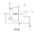
- Fig. 4b illustrates an alternate embodiment of a push/pull LDO 410.
- the push/pull LDO 410 illustrated in Fig. 4b may be based on a NMOS transistor T1.
- the other components in Fig. 4b may operate similarly to the push/pull LDO 400 illustrated in Fig. 4a .
- the push/pull LDO 410 may include an amplifier A1 and biasing resistors R1 and R2.
- the push/pull LDO 410 may further include push/pull drivers 412 and an NMOS transistor T2.
- the push/pull drivers 412 may drive the transistors T1 and T2 in a class-AB, class-B or class C configuration.
- the push/pull LDO 410 may be configured so that when current is flowing into the push/pull LDO 410 (through transistor T2), the output voltage at the V1 port is kept below Vmax. However, the additional components for sinking current may increase the quiescent current of the push/pull LDO 410.
- Fig. 5 illustrates an alternate embodiment of a push/pull LDO 500.
- the push/pull LDO 500 illustrated in Fig. 5 may include a source LDO 502 and a sink LDO 504.
- the source LDO 502 may include a PMOS transistor T1, an amplifier A1, and biasing resistors R1 and R2.
- the transistor T1 may be an NMOS transistor as described in Fig. 4a .
- the sink LDO 504 may be similar to the source LDO 502, but with a NMOS output transistor T2 connected to ground.
- a comparator C1 may compare the voltage at the V1 port to a threshold voltage Von.
- the comparator C1 may enable the sink LDO 504 by activating a switch SW1 when the voltage at the V1 port exceeds the threshold Von.
- an amplifier A2 may drive the transistor T2.
- the amplifier may be biased by resistors R3 and R4. Because the sink LDO 504 is only enabled when the voltage on the V1 port crosses a certain value (Von), the sink LDO 504 may not need to have a low quiescent current consumption, unlike the circuits illustrated in Figs. 4a and 4b .
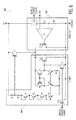
- Fig. 6 illustrates an embodiment of a combination circuit 600 that includes a clamp 602 and sink LDO 604.
- the combination circuit 600 may further include a high-voltage cascode transistor T1.
- the clamp 602 may limit the voltage at the V1 port to between a minimum voltage Vmin and a maximum voltage Vmax.
- the minimum voltage Vmin and maximum voltage Vmax may be determined by the design of the IC 204 and other system components.
- the clamp 602 may consume a maximum current of Imax when the clamp 602 is disabled.
- the sink LDO 604 may operate at close to the maximum voltage Vmax of the clamp 602. Both circuits may share the high-voltage cascode transistor T1 because transistor T1 may be relatively large in size compared to the clamp 602 and sink LDO 604 circuits.
- the clamp 602 may include transistors T2, T3, T4, T5, T6, T7, T8, T9, T10, T11, and T12, and resistors R1, R2, and R3.
- the sink LDO 604 may include a transistor T13, an amplifier A1, a switch SW1, and resistors R4 and R5.
- the combination circuit 600 may disable the clamp 602 when the sink LDO 604 is enabled, and enable the clamp 602 when the sink LDO is disabled.
- the clamp 602 may be enabled and the sink LDO disabled by a LOW enable/disable signal.
- the circuitry in the clamp 602 may function on a feedback loop which may regulate a voltage to approximately four times a bandgap voltage.
- the clamp 602 may be regulated to the condition that the current in transistor T9 equals the current in transistor T7 by driving the transistor T10 such that the current in transistors T1 and T10 equals the current at the V1 port.
- I T ⁇ 6 V T ⁇ ln 2 R ⁇ 3 V
- V ⁇ 1 4 ⁇ V BE + R ⁇ 1 + R ⁇ 2
- R ⁇ 3 ⁇ V T ⁇ ln ⁇ 2 4 ⁇ V BE + R ⁇ 1 + R ⁇ 2 4 ⁇ R ⁇ 3 ⁇ V T ⁇ ln ⁇ 2
- the output voltage at the V1 port may be regulated to 4 times a bandgap voltage (for example, approximately 4.8V).
- Resistors R1 and R2 may be used to bias the gate of the high-voltage cascode transistor T1.
- the high-voltage cascode transistor T1 may be biased such that the source voltage of the high-voltage cascode transistor T1 is lower than the maximum allowable voltage of the transistors used in the clamp 602 (for example, 3.3V).
- the resistors R1, R2 and R3 may have a high resistance, and may lower the current consumption of the clamp 602 when the clamp 602 is disabled.
- R1+R2 may be chosen to approximately equal 3M ⁇ .
- comparator may enables the sink LDO 604 and disable the clamp 602 by setting the enable/disable signal HIGH.
- the sink LDO 604 may use a reference voltage (for example, a bandgap voltage of 1.21V) which may then be multiplied with the ratio of resistors R4 andR5 by means of negative feedback.
- the amplifer A1 may drive transistor T13 which may sink a desired amount of current through the high-voltage cascode transistor T1.
- V V ⁇ 1 R ⁇ 4 + R ⁇ 5 R ⁇ 5 ⁇ V ref
- the combination circuit 600 may sink current from the V1 port and may maintain the voltage at the V1 port to within the desired Vmax and Vmin values.
- the combination circuit 600 may prevent damage to other system components, and may ensure other system components operate properly.
Landscapes
- Engineering & Computer Science (AREA)
- Physics & Mathematics (AREA)
- Electromagnetism (AREA)
- General Physics & Mathematics (AREA)
- Radar, Positioning & Navigation (AREA)
- Automation & Control Theory (AREA)
- Continuous-Control Power Sources That Use Transistors (AREA)
- Electronic Switches (AREA)
- Amplifiers (AREA)
- Dc-Dc Converters (AREA)
- Direct Current Feeding And Distribution (AREA)
Abstract
Description
- Various exemplary embodiments disclosed herein relate generally to circuitry for clamping voltage and sinking current.
- A voltage clamp may be used to adapt an input voltage signal to a component that cannot make use of or may be damaged by the voltage range of the original voltage input. A current sink is an electrical component or circuit that may drain current from other components.
- A brief summary of various exemplary embodiments is presented. Some simplifications and omissions may be made in the following summary, which is intended to highlight and introduce some aspects of the various exemplary embodiments, but not to limit the scope of the invention. Detailed descriptions of a preferred exemplary embodiment adequate to allow those of ordinary skill in the art to make and use the inventive concepts will follow in later sections.
- Various exemplary embodiments relate to a system for supplying power, including: an input/output port; a regulator, wherein the regulator supplies power to the input/output port in a first mode, sinks current from the input/output port in a second mode, and is disabled in a third mode; and a clamp, wherein the clamp is disabled in the first and second modes, and limits the voltage at the input/output port below a first value in the third mode.
- In some embodiments, the regulator limits the voltage at the input/output port to below the first value in the second mode. In some embodiments, the regulator is a push/pull low-dropout regulator. In some embodiments, the regulator includes a source regulator and a sink regulator. In some embodiments, the sink regulator is enabled when the voltage at the input/output port exceeds a threshold. In some embodiments, the first value is a voltage that would damage the system. In some embodiments, the regulator and the clamp are integrated in the same component. In some embodiments, the regulator supplies power to a microcontroller. In some embodiments, the microcontroller receives inputs from external switches. In some embodiments, the regulator limits a voltage from the external switches in the second mode, and wherein the clamp limits the voltage from the external switches in the third mode.
- Various exemplary embodiments further relate to a method for supplying power, including: supplying power to an input/output port by a regulator in a first mode; sinking current from the input/output port by the regulator in a second mode; disabling the regulator in a third mode; and limiting the voltage at the input/output port below a first value by a clamp in the third mode.
- In some embodiments, sinking current from the input/output port by the regulator includes limiting the voltage at the input/output port to below the first value in the second mode. In some embodiments, the regulator is a push/pull low-dropout regulator. In some embodiments, the regulator includes a source regulator and a sink regulator. In some embodiments, the method for supplying power further includes enabling the sink regulator when the voltage at the input/output port exceeds a threshold. In some embodiments, the regulator and the clamp are integrated in the same component. In some embodiments, the method for supplying power further includes supplying power to a micro controller by the regulator. In some embodiments, the micro controller receives inputs from external switches. In some embodiments, the method for supplying power further includes: limiting a voltage from the external switches by the regulator in the second mode; and limiting the voltage from the external switches by the clamp in the third mode.
- In order to better understand various exemplary embodiments, reference is made to the accompanying drawings, wherein:
-
Fig. 1 illustrates an embodiment of a conventional electronic control unit; -
Fig. 2 illustrates an electronic control unit according to an embodiment of the present invention; -
Fig. 3 illustrates an embodiment of a clamp; -
Fig. 4a illustrates an embodiment of a push/pull LDO regulator; -
Fig. 4b illustrates an alternate embodiment of a push/pull LDO regulator; -
Fig. 5 illustrates an alternate embodiment of a push/pull LDO regulator; and -
Fig. 6 illustrates an embodiment of a combination circuit. - Referring now to the drawings, in which like numerals refer to like components or steps, there are disclosed broad aspects of various exemplary embodiments.
- It should be appreciated by those skilled in the art that any block diagrams herein represent conceptual views of illustrative circuitry embodying the principals of the embodiments of the invention.
- According to the foregoing, various exemplary embodiments provide for a system and method for supplying power.
-
Fig. 1 illustrates an embodiment of a conventional electronic control unit (ECU) 100. The ECU 100 may include a micro controller (µC) 102 and an integrated circuit (IC) 104. The ECU 100,µC 102, and IC 104 maybe provided as integrated components or as separate components. TheIC 104 may receive an input voltage Vin1 from a direct current voltage source, such as, for example, a 12V vehicle battery. A diode D1 may aid in decoupling theIC 104 from the power source. The IC 104 may include a low-dropout regulator (LDO) 106. TheLDO 106 may regulate the input voltage Vin1 and may output a constant voltage from an input/output port V1 for powering theµC 102. The voltage for powering theµC 102 may be input at the Vdd port of theµC 102. A zener diode D2 may be connected between ground and the V1 and Vdd ports of theIC 104 andµC 102. Input ports (P1, P2) of theµC 102 may be connected to one or more switches (SW1, SW2). The input ports may detect if one or more of the switches (SW1, SW2) is open or closed. The switches SW1 and SW2 may be switches within an automotive vehicle. While two switches are illustrated inFig. 1 , more switches may be connected depending on the capabilities of theµC 102. Pull-up resistors R1 and R2 may cause the voltage applied to the input ports P1 and P2 to be proportional to an input voltage Vin2 when the corresponding switch (SW1, SW2) is open. The input voltage Vin2 maybe supplied by a direct current voltage source, such as, for example a 12V vehicle battery. The input voltages Vin1 and Vin2 may be supplied by the same voltage source or different voltages sources. Resistors R3 and R4 may limit the current flowing inECU 100. Diodes D3 and D4 may protect theµC 102 from electrostatic discharge (ESD). - The voltage supplied by Vin2 to the input ports P 1 and P2 of the
µC 102 may be a large voltage that may damage theµC 102. For example, the voltage supplied by a 12V vehicle battery may have a voltage supply range of up to 40V. The zener diode D2 may protect theµC 102 when a large voltage is supplied to one or more of the input ports P1 and P2. The input ports P1 and P2 may be connected to the zener diode D2 via the ESD diodes D3 and D4. The zener diode D1, and ESD diodes D3 and D4 may form a clamp that may limit the voltage on the input ports P1 and P2. The current (Isink) flowing into the zener diode D2 may be limited by the resistors R3 and R4. The zener voltage of the zener diode D2 may be chosen to be higher than the maximum output voltage of theLDO 106. For example, if the maximum output voltage of theLDO 106 is 5.5V, then the zener voltage may be chosen to be 7V to account for voltage spread and the maximum Isink current. TheIC 104 in aconventional ECU 100 may be designed to passively withstand the voltage at the V1 port. The voltage that theIC 104 may withstand may be dependent on the manufacturing process of the IC. For example, an ABCD3 manufacturing process may include 5V CMOS components. An IC manufactured with the ABCD3 process may be able to passively withstand a voltage of 7V. - However, in some embodiments, the
IC 104 may not be capable of withstanding certain voltages at the V1 port, and theIC 104 may fail or be damaged when one or more switches (SW1, SW2) is open. For example, an IC manufactured using the ABCD9 process may include CMOS14 based components with a breakdown voltage of 3.6V. An IC manufactured using the ABCD9 process may have a maximum voltage of 6V and may be damaged at 7V. Therefore, it may be desirable to limit the voltage at the V1 port to below the maximum voltage of the IC. - Alternatively, the use of an external zener diode D2 may not be desirable to a system designer due to cost and component size considerations. Therefore, it may be desirable for the the clamping function of the external zener diode D2 to be incorporated into an IC.
-
Fig. 2 illustrates an electronic control unit (ECU) 200 according to an embodiment of the present invention. TheECU 200 may include a micro controller (µC) 202 and an integrated circuit (IC) 204. TheECU 200,µC 202, andIC 204 may be provided as integrated components or as separate components. TheIC 204 may receive an input voltage Vin1 from a direct current voltage source, such as, for example, a 12V vehicle battery. A diode D1 may aid in decoupling theIC 204 from the power source. TheIC 204 may include a push/pull low-dropout regulator (LDO) 206. The push/pull LDO 206 may regulate the input voltage Vin1 and may output a constant voltage from an input/output port V1 for powering theµC 202. The voltage for powering theµC 202 may be input at the Vdd port of theµC 202. TheIC 204 may further include aninternal clamp 208. Theinternal clamp 208 may be connected to the V1 port of theIC 204. TheIC 204 may further include switches SW3 and SW4 for enabling/disabling the push/pull LDO 206 and theinternal clamp 208. The switches SW3 and SW4 may be activated by an enable/disable signal. The enable/disable signal may be supplied by digital logic circuitry (not shown) in theIC 202. - Input ports (P1, P2) of the
µC 202 may be connected to one or more switches (SW1, SW2). The input ports may detect if one or more of the switches (SW1, SW2) is open or closed. The switches SW1 and SW2 may be switches within an automotive vehicle. While two switches are illustrated inFig. 2 , more switches may be connected depending on the capabilities of theµC 202. Pull-up resistors R1 and R2 may cause the voltage applied to the input ports P1 and P2 to be proportional to an input voltage Vin2 when the corresponding switch (SW1, SW2) is open. The input voltage Vin2 may be supplied by a direct current voltage source, such as, for example a 12V vehicle battery. The input voltages Vin1 and Vin2 may be supplied by the same voltage source or different voltages sources. Resistors R3 and R4 may limit the current flowing inECU 200. Diodes D3 and D4 may protect theµC 102 from electrostatic discharge (ESD). - The voltage supplied by Vin2 to the input ports P 1 and P2 of the
µC 202 may be a large voltage that may damage theµC 202. For example, the voltage supplied by a 12V vehicle battery may have a voltage supply range of up to 40V. The circuitry in theIC 204 may protect theµC 202 when a large voltage is supplied to one or more of the input ports P1 and P2. The input ports P 1 and P2 may be connected to the V1 port of theIC 204 via the ESD diodes D3 and D4. The current (Isink) flowing into theIC 204 may be limited by the resistors R3 and R4. - The
clamp 208 may be enabled when the push/pullLDO 206 is disabled or when theIC 204 is not receiving an input voltage Vin1. Theclamp 208 may be disabled when the push/pullLDO 206 is enabled. Theclamp 208 may function when a voltage is present at only the V1 port of theIC 204. Theclamp 208 may protect theµC 202 when the push/pullLDO 206 is disabled (for example, when the voltage from Vin1 is very low or unavailable). The push/pull LDO 206 may protect theµC 202 when the clamp is disabled. When theclamp 208 is enabled, the voltage at the V1 port may be clamped to between 0V and a voltage below the maximum voltage theIC 204 can withstand (Vmax). When the push/pullLDO 206 is enabled, the voltage at the V1 port maybe held within a minimum and maximum range (Vmin and Vmax). - The push/
pull LDO 206 may be capable of both sourcing current and sinking current. When the push/pullLDO 206 is enabled and theclamp 208 is disabled, the push/pull LDO 206 may sink excess current from the V1 port of theIC 206. The push/pull LDO 206 may be designed to sink the maximum reverse current allowed by theµC 202. -
Fig. 3 illustrates an embodiment of aclamp circuit 300. Theclamp circuit 300 may include a cascode oflow-voltage NMOS transistors T1 and T2. Transistor T3 may enable/disable theclamp circuit 300. When transistor T3 is open (enable/disable signal = LOW), the output voltage at the V1 port may be the Vgs voltage of transistor T2. Depending on the size of transistor T2 and the drain current, the voltage at the V1 port may be much lower than Vmax. When the clamp is disabled (enable/disable signal = HIGH), the current consumption of theclamp circuit 300 maybe limited by resistors R1 and R2. Resistors R1 and R2 may have a large value to limit the current consumption to an acceptable level. While NMOS transistors are shown inFig. 3 , other types of clamping technology may be used for theclamp 208 illustrated inFig. 2 . -
Fig. 4a illustrates an embodiment of a push/pull LDO 400. The push/pullLDO 400 illustrated inFig. 4a may be based on a PMOS transistor T1. The push/pull LDO 400 may include an amplifier A1 and biasing resistors R1 and R2. In order for the push/pull LDO 400 to sink current, the push/pull LDO 400 may further include push/pulldrivers 402 and an NMOS transistor T2. The push/pulldrivers 402 may drive the transistors T1 and T2 in a class-AB, class-B or class C configuration. The push/pull LDO 400 may be configured so that when current is flowing into the push/pull LDO 400 (through transistor T2), the output voltage at the V1 port is kept below Vmax. However, the additional components for sinking current may increase the quiescent current of the push/pull LDO 400. -
Fig. 4b illustrates an alternate embodiment of a push/pull LDO 410. The push/pullLDO 410 illustrated inFig. 4b may be based on a NMOS transistor T1. The other components inFig. 4b may operate similarly to the push/pull LDO 400 illustrated inFig. 4a . The push/pull LDO 410 may include an amplifier A1 and biasing resistors R1 and R2. In order for the push/pull LDO 410 to sink current, the push/pull LDO 410 may further include push/pulldrivers 412 and an NMOS transistor T2. The push/pulldrivers 412 may drive the transistors T1 and T2 in a class-AB, class-B or class C configuration. The push/pull LDO 410 may be configured so that when current is flowing into the push/pull LDO 410 (through transistor T2), the output voltage at the V1 port is kept below Vmax. However, the additional components for sinking current may increase the quiescent current of the push/pull LDO 410. -
Fig. 5 illustrates an alternate embodiment of a push/pull LDO 500. The push/pullLDO 500 illustrated inFig. 5 may include asource LDO 502 and asink LDO 504. Thesource LDO 502 may include a PMOS transistor T1, an amplifier A1, and biasing resistors R1 and R2. Alternatively, the transistor T1 may be an NMOS transistor as described inFig. 4a . Thesink LDO 504 may be similar to thesource LDO 502, but with a NMOS output transistor T2 connected to ground. A comparator C1 may compare the voltage at the V1 port to a threshold voltage Von. The comparator C1 may enable thesink LDO 504 by activating a switch SW1 when the voltage at the V1 port exceeds the threshold Von. When thesink LDO 504 is enabled, an amplifier A2 may drive the transistor T2. The amplifier may be biased by resistors R3 and R4. Because thesink LDO 504 is only enabled when the voltage on the V1 port crosses a certain value (Von), thesink LDO 504 may not need to have a low quiescent current consumption, unlike the circuits illustrated inFigs. 4a and4b . -
Fig. 6 illustrates an embodiment of acombination circuit 600 that includes aclamp 602 and sinkLDO 604. Thecombination circuit 600 may further include a high-voltage cascode transistor T1. Theclamp 602 may limit the voltage at the V1 port to between a minimum voltage Vmin and a maximum voltage Vmax. The minimum voltage Vmin and maximum voltage Vmax may be determined by the design of theIC 204 and other system components. Theclamp 602 may consume a maximum current of Imax when theclamp 602 is disabled. Thesink LDO 604 may operate at close to the maximum voltage Vmax of theclamp 602. Both circuits may share the high-voltage cascode transistor T1 because transistor T1 may be relatively large in size compared to theclamp 602 and sinkLDO 604 circuits. - The
clamp 602 may include transistors T2, T3, T4, T5, T6, T7, T8, T9, T10, T11, and T12, and resistors R1, R2, and R3. Thesink LDO 604 may include a transistor T13, an amplifier A1, a switch SW1, and resistors R4 and R5. - Similarly to the system described in
Fig. 2 , thecombination circuit 600 may disable theclamp 602 when thesink LDO 604 is enabled, and enable theclamp 602 when the sink LDO is disabled. Theclamp 602 may be enabled and the sink LDO disabled by a LOW enable/disable signal. When theclamp 602 is enabled and thesink LDO 604 is disabled, the circuitry in theclamp 602 may function on a feedback loop which may regulate a voltage to approximately four times a bandgap voltage. Theclamp 602 may be regulated to the condition that the current in transistor T9 equals the current in transistor T7 by driving the transistor T10 such that the current in transistors T1 and T10 equals the current at the V1 port. The following equations may be used to calculate values in thecombination circuit 600 when the clamp is enabled:


- The output voltage at the V1 port may be regulated to 4 times a bandgap voltage (for example, approximately 4.8V). Resistors R1 and R2 may be used to bias the gate of the high-voltage cascode transistor T1. The high-voltage cascode transistor T1 may be biased such that the source voltage of the high-voltage cascode transistor T1 is lower than the maximum allowable voltage of the transistors used in the clamp 602 (for example, 3.3V). The resistors R1, R2 and R3 may have a high resistance, and may lower the current consumption of the
clamp 602 when theclamp 602 is disabled. The value of the resistors R1 and R2 may be determined using the following equation:
- For example, if the voltage at the V1 port is 5V, and the current is 1µA, then R1+R2 may be chosen to approximately equal 3MΩ.
- When a separate comparator (not shown) detects that the voltage at the V1 port is above a certain threshold (for example, 5.5V), comparator may enables the
sink LDO 604 and disable theclamp 602 by setting the enable/disable signal HIGH. Thesink LDO 604 may use a reference voltage (for example, a bandgap voltage of 1.21V) which may then be multiplied with the ratio of resistors R4 andR5 by means of negative feedback. The amplifer A1 may drive transistor T13 which may sink a desired amount of current through the high-voltage cascode transistor T1. The following equation may be used to calculate the voltage at the V1 port when thesink LDO 604 is enabled:
- The
combination circuit 600 may sink current from the V1 port and may maintain the voltage at the V1 port to within the desired Vmax and Vmin values. Thecombination circuit 600 may prevent damage to other system components, and may ensure other system components operate properly. - Although the various exemplary embodiments have been described in detail with particular reference to certain exemplary aspects thereof, it should be understood that the invention is capable of other embodiments and its details are capable of modifications in various obvious respects. As is readily apparent to those skilled in the art, variations and modifications can be affected while remaining within the spirit and scope of the invention. Accordingly, the foregoing disclosure, description, and figures are for illustrative purposes only and do not in any way limit the invention, which is defined only by the claims.
Claims (15)
- A system for supplying power, comprising:an input/output port;a regulator, wherein the regulator supplies power to the input/output port in a first mode, sinks current from the input/output port in a second mode, and is disabled in a third mode; anda clamp, wherein the clamp is disabled in the first and second modes, and limits the voltage at the input/output port below a first value in the third mode.
- The system for supplying power of claim 1, wherein the regulator limits the voltage at the input/output port to below the first value in the second mode.
- The system for supplying power of claim 1, wherein the regulator is a push/pull low-dropout regulator.
- The system for supplying power of claim 1, wherein the regulator includes a source regulator and a sink regulator.
- The system for supplying power of claim 4, wherein the sink regulator is enabled when the voltage at the input/output port exceeds a threshold.
- The system for supplying power of claim 1, wherein the first value is a voltage that would damage the system.
- The system for supplying power of claim 1, wherein the regulator and the clamp are integrated in the same component.
- The system for supplying power of claim 1, wherein the regulator supplies power to a microcontroller.
- The system for supplying power of claim 8, wherein the microcontrollerreceives inputs from external switches.
- The system for supplying power of claim 9, wherein the regulator limits a voltage from the external switches in the second mode, and wherein the clamp limits the voltage from the external switches in the third mode.
- A method for supplying power, comprising:supplying power to an input/output port by a regulator in a first mode;sinking current from the input/output port by the regulator in a second mode;disabling the regulator in a third mode; andlimiting the voltage at the input/output port below a first value by a clamp in the third mode.
- The method for supplying power of claim 11, wherein sinking current from the input/output port by the regulator includes limiting the voltage at the input/output port to below the first value in the second mode.
- The method for supplying power of claim 11, wherein the regulator is a push/pull low-dropout regulator.
- The method for supplying power of claim 11, wherein the regulator includes a source regulator and a sink regulator.
- The method for supplying power of claim 14, further comprising:enabling the sink regulator when the voltage at the input/output port exceeds a threshold.
Applications Claiming Priority (1)
| Application Number | Priority Date | Filing Date | Title |
|---|---|---|---|
| US13/292,214 US9651967B2 (en) | 2011-11-09 | 2011-11-09 | Power supply with integrated voltage clamp and current sink |
Publications (2)
| Publication Number | Publication Date |
|---|---|
| EP2592520A2 true EP2592520A2 (en) | 2013-05-15 |
| EP2592520A3 EP2592520A3 (en) | 2016-08-10 |
Family
ID=47215344
Family Applications (1)
| Application Number | Title | Priority Date | Filing Date |
|---|---|---|---|
| EP12181522.9A Withdrawn EP2592520A3 (en) | 2011-11-09 | 2012-08-23 | Power supply with integrated voltage clamp and current sink |
Country Status (3)
| Country | Link |
|---|---|
| US (1) | US9651967B2 (en) |
| EP (1) | EP2592520A3 (en) |
| CN (1) | CN103107690B (en) |
Families Citing this family (11)
| Publication number | Priority date | Publication date | Assignee | Title |
|---|---|---|---|---|
| US9525337B2 (en) | 2014-04-24 | 2016-12-20 | Qualcomm Incorporated | Charge-recycling circuits |
| US9680371B2 (en) | 2014-04-24 | 2017-06-13 | Qualcomm Incorporated | Charge pumps having variable gain and variable frequency |
| US9276562B2 (en) | 2014-04-24 | 2016-03-01 | Qualcomm, Incorporated | Charge-recycling circuits including switching power stages with floating rails |
| EP2952996B1 (en) | 2014-06-02 | 2019-03-13 | Dialog Semiconductor (UK) Limited | A current sink stage for LDO |
| CN104135213A (en) * | 2014-07-31 | 2014-11-05 | 苏州汇川技术有限公司 | Motor controller with short circuit protection function and motor control system with motor controller |
| CN110058632B (en) * | 2014-12-29 | 2025-04-11 | 意法半导体研发(深圳)有限公司 | Low Dropout Amplifier |
| US9588540B2 (en) | 2015-09-10 | 2017-03-07 | Freescale Semiconductor, Inc. | Supply-side voltage regulator |
| US9780783B1 (en) | 2016-03-31 | 2017-10-03 | Intel Corporation | Voltage tolerant termination presence detection |
| GB2550977B (en) * | 2016-05-31 | 2020-07-22 | Cirrus Logic Int Semiconductor Ltd | Monitoring of devices |
| GB2557222A (en) | 2016-11-30 | 2018-06-20 | Nordic Semiconductor Asa | Voltage regulator |
| US12326747B1 (en) * | 2022-12-16 | 2025-06-10 | Cadence Design Systems, Inc. | Dual-mode low dropout regulator with fast transient switching between modes |
Citations (1)
| Publication number | Priority date | Publication date | Assignee | Title |
|---|---|---|---|---|
| US20080012542A1 (en) * | 2006-07-11 | 2008-01-17 | Jiangang Liu | DC-DC converter with over-voltage protection |
Family Cites Families (12)
| Publication number | Priority date | Publication date | Assignee | Title |
|---|---|---|---|---|
| US6201375B1 (en) | 2000-04-28 | 2001-03-13 | Burr-Brown Corporation | Overvoltage sensing and correction circuitry and method for low dropout voltage regulator |
| US6583610B2 (en) * | 2001-03-12 | 2003-06-24 | Semtech Corporation | Virtual ripple generation in switch-mode power supplies |
| US20070075692A1 (en) | 2001-08-31 | 2007-04-05 | Ostrom Kenneth R | Methods and apparatus for current-controlled transient regulation |
| DE10332578B4 (en) * | 2002-08-06 | 2008-05-29 | Siemens Ag | Protection circuit and a method for operating the protection circuit, in particular for overvoltage protection of an electronic control system for a motor vehicle |
| US6707280B1 (en) | 2002-09-09 | 2004-03-16 | Arques Technology, Inc. | Bidirectional voltage regulator sourcing and sinking current for line termination |
| WO2005085969A1 (en) * | 2004-02-05 | 2005-09-15 | Monolithic Power Systems Inc. | A dc/dc voltage regulator with automatic current sensing selectability for linear and switch mode operation utilizing a single voltage reference |
| US7148670B2 (en) * | 2005-01-18 | 2006-12-12 | Micrel, Inc. | Dual mode buck regulator with improved transition between LDO and PWM operation |
| US7504807B2 (en) * | 2005-02-09 | 2009-03-17 | Panasonic Corporation | Switching regulator with voltage step up or pass in standby mode and with voltage step up/step down in normal operation mode |
| CN101398694A (en) | 2007-09-30 | 2009-04-01 | Nxp股份有限公司 | Non-capacitance low voltage difference constant voltage regulator with rapid excess voltage response |
| US7679341B2 (en) * | 2007-12-12 | 2010-03-16 | Monolithic Power Systems, Inc. | External control mode step down switching regulator |
| US7830128B2 (en) * | 2008-07-31 | 2010-11-09 | Monolithic Power Systems, Inc. | Switching regulator circuit for operation as a switching device in a switching mode and a passive device in a passive mode |
| US8378652B2 (en) * | 2008-12-23 | 2013-02-19 | Texas Instruments Incorporated | Load transient response time of LDOs with NMOS outputs with a voltage controlled current source |
-
2011
- 2011-11-09 US US13/292,214 patent/US9651967B2/en active Active
-
2012
- 2012-08-23 EP EP12181522.9A patent/EP2592520A3/en not_active Withdrawn
- 2012-11-06 CN CN201210438735.3A patent/CN103107690B/en active Active
Patent Citations (1)
| Publication number | Priority date | Publication date | Assignee | Title |
|---|---|---|---|---|
| US20080012542A1 (en) * | 2006-07-11 | 2008-01-17 | Jiangang Liu | DC-DC converter with over-voltage protection |
Also Published As
| Publication number | Publication date |
|---|---|
| CN103107690B (en) | 2016-01-20 |
| EP2592520A3 (en) | 2016-08-10 |
| CN103107690A (en) | 2013-05-15 |
| US9651967B2 (en) | 2017-05-16 |
| US20130113446A1 (en) | 2013-05-09 |
Similar Documents
| Publication | Publication Date | Title |
|---|---|---|
| EP2592520A2 (en) | Power supply with integrated voltage clamp and current sink | |
| US9454166B2 (en) | LDO regulator with improved load transient performance for internal power supply | |
| US7626792B2 (en) | Power supply control apparatus including highly-reliable overcurrent detecting circuit | |
| US10067554B2 (en) | VCONN pull-down circuits and related methods for USB type-C connections | |
| US9405309B2 (en) | Dual mode low-dropout linear regulator | |
| US8164378B2 (en) | Device and technique for transistor well biasing | |
| EP2952996B1 (en) | A current sink stage for LDO | |
| US10168363B1 (en) | Current sensor with extended voltage range | |
| US20100176875A1 (en) | Method for Improving Power-Supply Rejection | |
| CN102455730A (en) | Semiconductor integrated circuit for regulator | |
| US8704506B2 (en) | Voltage regulator soft-start circuit providing reference voltage ramp-up | |
| CN104135237B (en) | Gate driving circuit | |
| US8829952B2 (en) | Gate drive circuit | |
| US9800233B1 (en) | Voltage clamp circuits and related methods | |
| US8766679B1 (en) | Power on reset (POR) circuit | |
| EP2503690B1 (en) | Backdrive protection circuit | |
| CN112513771B (en) | Dual Input LDO Voltage Regulator | |
| CN111034048A (en) | High voltage output driver for a sensor device with reverse current blocking | |
| EP2592527A2 (en) | Power supply with extended minimum voltage output | |
| US10651641B2 (en) | Electronic device protection circuit, corresponding device and method | |
| CN105955385A (en) | High pressure resistant linear voltage regulator based on standard CMOS technology | |
| US20110095737A1 (en) | Voltage regulator, and integrated circuit using the same | |
| EP2876812A1 (en) | Input circuit with mirroring | |
| CN205608579U (en) | High pressure resistant linear voltage regulator based on standard CMOS technology | |
| US9287856B2 (en) | Tracking circuit |
Legal Events
| Date | Code | Title | Description |
|---|---|---|---|
| PUAI | Public reference made under article 153(3) epc to a published international application that has entered the european phase |
Free format text: ORIGINAL CODE: 0009012 |
|
| AK | Designated contracting states |
Kind code of ref document: A2 Designated state(s): AL AT BE BG CH CY CZ DE DK EE ES FI FR GB GR HR HU IE IS IT LI LT LU LV MC MK MT NL NO PL PT RO RS SE SI SK SM TR |
|
| AX | Request for extension of the european patent |
Extension state: BA ME |
|
| 17P | Request for examination filed |
Effective date: 20140331 |
|
| PUAL | Search report despatched |
Free format text: ORIGINAL CODE: 0009013 |
|
| AK | Designated contracting states |
Kind code of ref document: A3 Designated state(s): AL AT BE BG CH CY CZ DE DK EE ES FI FR GB GR HR HU IE IS IT LI LT LU LV MC MK MT NL NO PL PT RO RS SE SI SK SM TR |
|
| AX | Request for extension of the european patent |
Extension state: BA ME |
|
| RIC1 | Information provided on ipc code assigned before grant |
Ipc: G05F 1/571 20060101AFI20160704BHEP Ipc: G05F 1/595 20060101ALI20160704BHEP Ipc: G05F 1/618 20060101ALI20160704BHEP Ipc: G05F 1/613 20060101ALI20160704BHEP |
|
| RBV | Designated contracting states (corrected) |
Designated state(s): AL AT BE BG CH CY CZ DE DK EE ES FI FR GB GR HR HU IE IS IT LI LT LU LV MC MK MT NL NO PL PT RO RS SE SI SK SM TR |
|
| STAA | Information on the status of an ep patent application or granted ep patent |
Free format text: STATUS: EXAMINATION IS IN PROGRESS |
|
| 17Q | First examination report despatched |
Effective date: 20181219 |
|
| STAA | Information on the status of an ep patent application or granted ep patent |
Free format text: STATUS: THE APPLICATION IS DEEMED TO BE WITHDRAWN |
|
| 18D | Application deemed to be withdrawn |
Effective date: 20210504 |