EP2590217A2 - Stacked packages using laser direct structuring - Google Patents
Stacked packages using laser direct structuring Download PDFInfo
- Publication number
- EP2590217A2 EP2590217A2 EP20120190418 EP12190418A EP2590217A2 EP 2590217 A2 EP2590217 A2 EP 2590217A2 EP 20120190418 EP20120190418 EP 20120190418 EP 12190418 A EP12190418 A EP 12190418A EP 2590217 A2 EP2590217 A2 EP 2590217A2
- Authority
- EP
- European Patent Office
- Prior art keywords
- lds
- attached
- package
- die
- substrate
- Prior art date
- Legal status (The legal status is an assumption and is not a legal conclusion. Google has not performed a legal analysis and makes no representation as to the accuracy of the status listed.)
- Ceased
Links
Images




Classifications
-
- H—ELECTRICITY
- H05—ELECTRIC TECHNIQUES NOT OTHERWISE PROVIDED FOR
- H05K—PRINTED CIRCUITS; CASINGS OR CONSTRUCTIONAL DETAILS OF ELECTRIC APPARATUS; MANUFACTURE OF ASSEMBLAGES OF ELECTRICAL COMPONENTS
- H05K1/00—Printed circuits
- H05K1/02—Details
- H05K1/0296—Conductive pattern lay-out details not covered by sub groups H05K1/02 - H05K1/0295
-
- H—ELECTRICITY
- H05—ELECTRIC TECHNIQUES NOT OTHERWISE PROVIDED FOR
- H05K—PRINTED CIRCUITS; CASINGS OR CONSTRUCTIONAL DETAILS OF ELECTRIC APPARATUS; MANUFACTURE OF ASSEMBLAGES OF ELECTRICAL COMPONENTS
- H05K1/00—Printed circuits
- H05K1/02—Details
- H05K1/11—Printed elements for providing electric connections to or between printed circuits
- H05K1/111—Pads for surface mounting, e.g. lay-out
-
- H—ELECTRICITY
- H10—SEMICONDUCTOR DEVICES; ELECTRIC SOLID-STATE DEVICES NOT OTHERWISE PROVIDED FOR
- H10W—GENERIC PACKAGES, INTERCONNECTIONS, CONNECTORS OR OTHER CONSTRUCTIONAL DETAILS OF DEVICES COVERED BY CLASS H10
- H10W74/00—Encapsulations, e.g. protective coatings
- H10W74/40—Encapsulations, e.g. protective coatings characterised by their materials
- H10W74/47—Encapsulations, e.g. protective coatings characterised by their materials comprising organic materials, e.g. plastics or resins
- H10W74/473—Encapsulations, e.g. protective coatings characterised by their materials comprising organic materials, e.g. plastics or resins containing a filler
-
- H—ELECTRICITY
- H10—SEMICONDUCTOR DEVICES; ELECTRIC SOLID-STATE DEVICES NOT OTHERWISE PROVIDED FOR
- H10W—GENERIC PACKAGES, INTERCONNECTIONS, CONNECTORS OR OTHER CONSTRUCTIONAL DETAILS OF DEVICES COVERED BY CLASS H10
- H10W90/00—Package configurations
-
- H—ELECTRICITY
- H10—SEMICONDUCTOR DEVICES; ELECTRIC SOLID-STATE DEVICES NOT OTHERWISE PROVIDED FOR
- H10W—GENERIC PACKAGES, INTERCONNECTIONS, CONNECTORS OR OTHER CONSTRUCTIONAL DETAILS OF DEVICES COVERED BY CLASS H10
- H10W70/00—Package substrates; Interposers; Redistribution layers [RDL]
- H10W70/01—Manufacture or treatment
- H10W70/05—Manufacture or treatment of insulating or insulated package substrates, or of interposers, or of redistribution layers
- H10W70/093—Connecting or disconnecting other interconnections thereto or therefrom, e.g. connecting bond wires or bumps
-
- H—ELECTRICITY
- H10—SEMICONDUCTOR DEVICES; ELECTRIC SOLID-STATE DEVICES NOT OTHERWISE PROVIDED FOR
- H10W—GENERIC PACKAGES, INTERCONNECTIONS, CONNECTORS OR OTHER CONSTRUCTIONAL DETAILS OF DEVICES COVERED BY CLASS H10
- H10W70/00—Package substrates; Interposers; Redistribution layers [RDL]
- H10W70/40—Leadframes
-
- H—ELECTRICITY
- H10—SEMICONDUCTOR DEVICES; ELECTRIC SOLID-STATE DEVICES NOT OTHERWISE PROVIDED FOR
- H10W—GENERIC PACKAGES, INTERCONNECTIONS, CONNECTORS OR OTHER CONSTRUCTIONAL DETAILS OF DEVICES COVERED BY CLASS H10
- H10W70/00—Package substrates; Interposers; Redistribution layers [RDL]
- H10W70/60—Insulating or insulated package substrates; Interposers; Redistribution layers
-
- H—ELECTRICITY
- H10—SEMICONDUCTOR DEVICES; ELECTRIC SOLID-STATE DEVICES NOT OTHERWISE PROVIDED FOR
- H10W—GENERIC PACKAGES, INTERCONNECTIONS, CONNECTORS OR OTHER CONSTRUCTIONAL DETAILS OF DEVICES COVERED BY CLASS H10
- H10W72/00—Interconnections or connectors in packages
- H10W72/01—Manufacture or treatment
- H10W72/0198—Manufacture or treatment batch processes
-
- H—ELECTRICITY
- H10—SEMICONDUCTOR DEVICES; ELECTRIC SOLID-STATE DEVICES NOT OTHERWISE PROVIDED FOR
- H10W—GENERIC PACKAGES, INTERCONNECTIONS, CONNECTORS OR OTHER CONSTRUCTIONAL DETAILS OF DEVICES COVERED BY CLASS H10
- H10W72/00—Interconnections or connectors in packages
- H10W72/50—Bond wires
- H10W72/551—Materials of bond wires
- H10W72/552—Materials of bond wires comprising metals or metalloids, e.g. silver
- H10W72/5522—Materials of bond wires comprising metals or metalloids, e.g. silver comprising gold [Au]
-
- H—ELECTRICITY
- H10—SEMICONDUCTOR DEVICES; ELECTRIC SOLID-STATE DEVICES NOT OTHERWISE PROVIDED FOR
- H10W—GENERIC PACKAGES, INTERCONNECTIONS, CONNECTORS OR OTHER CONSTRUCTIONAL DETAILS OF DEVICES COVERED BY CLASS H10
- H10W72/00—Interconnections or connectors in packages
- H10W72/851—Dispositions of multiple connectors or interconnections
- H10W72/874—On different surfaces
- H10W72/884—Die-attach connectors and bond wires
-
- H—ELECTRICITY
- H10—SEMICONDUCTOR DEVICES; ELECTRIC SOLID-STATE DEVICES NOT OTHERWISE PROVIDED FOR
- H10W—GENERIC PACKAGES, INTERCONNECTIONS, CONNECTORS OR OTHER CONSTRUCTIONAL DETAILS OF DEVICES COVERED BY CLASS H10
- H10W74/00—Encapsulations, e.g. protective coatings
- H10W74/01—Manufacture or treatment
- H10W74/014—Manufacture or treatment using batch processing
-
- H—ELECTRICITY
- H10—SEMICONDUCTOR DEVICES; ELECTRIC SOLID-STATE DEVICES NOT OTHERWISE PROVIDED FOR
- H10W—GENERIC PACKAGES, INTERCONNECTIONS, CONNECTORS OR OTHER CONSTRUCTIONAL DETAILS OF DEVICES COVERED BY CLASS H10
- H10W74/00—Encapsulations, e.g. protective coatings
- H10W74/10—Encapsulations, e.g. protective coatings characterised by their shape or disposition
- H10W74/111—Encapsulations, e.g. protective coatings characterised by their shape or disposition the semiconductor body being completely enclosed
- H10W74/114—Encapsulations, e.g. protective coatings characterised by their shape or disposition the semiconductor body being completely enclosed by a substrate and the encapsulations
- H10W74/117—Encapsulations, e.g. protective coatings characterised by their shape or disposition the semiconductor body being completely enclosed by a substrate and the encapsulations the substrate having spherical bumps for external connection
-
- H—ELECTRICITY
- H10—SEMICONDUCTOR DEVICES; ELECTRIC SOLID-STATE DEVICES NOT OTHERWISE PROVIDED FOR
- H10W—GENERIC PACKAGES, INTERCONNECTIONS, CONNECTORS OR OTHER CONSTRUCTIONAL DETAILS OF DEVICES COVERED BY CLASS H10
- H10W90/00—Package configurations
- H10W90/701—Package configurations characterised by the relative positions of pads or connectors relative to package parts
- H10W90/721—Package configurations characterised by the relative positions of pads or connectors relative to package parts of bump connectors
- H10W90/724—Package configurations characterised by the relative positions of pads or connectors relative to package parts of bump connectors between a chip and a stacked insulating package substrate, interposer or RDL
-
- H—ELECTRICITY
- H10—SEMICONDUCTOR DEVICES; ELECTRIC SOLID-STATE DEVICES NOT OTHERWISE PROVIDED FOR
- H10W—GENERIC PACKAGES, INTERCONNECTIONS, CONNECTORS OR OTHER CONSTRUCTIONAL DETAILS OF DEVICES COVERED BY CLASS H10
- H10W90/00—Package configurations
- H10W90/701—Package configurations characterised by the relative positions of pads or connectors relative to package parts
- H10W90/721—Package configurations characterised by the relative positions of pads or connectors relative to package parts of bump connectors
- H10W90/726—Package configurations characterised by the relative positions of pads or connectors relative to package parts of bump connectors between a chip and a stacked lead frame, conducting package substrate or heat sink
-
- H—ELECTRICITY
- H10—SEMICONDUCTOR DEVICES; ELECTRIC SOLID-STATE DEVICES NOT OTHERWISE PROVIDED FOR
- H10W—GENERIC PACKAGES, INTERCONNECTIONS, CONNECTORS OR OTHER CONSTRUCTIONAL DETAILS OF DEVICES COVERED BY CLASS H10
- H10W90/00—Package configurations
- H10W90/701—Package configurations characterised by the relative positions of pads or connectors relative to package parts
- H10W90/731—Package configurations characterised by the relative positions of pads or connectors relative to package parts of die-attach connectors
- H10W90/734—Package configurations characterised by the relative positions of pads or connectors relative to package parts of die-attach connectors between a chip and a stacked insulating package substrate, interposer or RDL
-
- H—ELECTRICITY
- H10—SEMICONDUCTOR DEVICES; ELECTRIC SOLID-STATE DEVICES NOT OTHERWISE PROVIDED FOR
- H10W—GENERIC PACKAGES, INTERCONNECTIONS, CONNECTORS OR OTHER CONSTRUCTIONAL DETAILS OF DEVICES COVERED BY CLASS H10
- H10W90/00—Package configurations
- H10W90/701—Package configurations characterised by the relative positions of pads or connectors relative to package parts
- H10W90/731—Package configurations characterised by the relative positions of pads or connectors relative to package parts of die-attach connectors
- H10W90/736—Package configurations characterised by the relative positions of pads or connectors relative to package parts of die-attach connectors between a chip and a stacked lead frame, conducting package substrate or heat sink
-
- H—ELECTRICITY
- H10—SEMICONDUCTOR DEVICES; ELECTRIC SOLID-STATE DEVICES NOT OTHERWISE PROVIDED FOR
- H10W—GENERIC PACKAGES, INTERCONNECTIONS, CONNECTORS OR OTHER CONSTRUCTIONAL DETAILS OF DEVICES COVERED BY CLASS H10
- H10W90/00—Package configurations
- H10W90/701—Package configurations characterised by the relative positions of pads or connectors relative to package parts
- H10W90/751—Package configurations characterised by the relative positions of pads or connectors relative to package parts of bond wires
- H10W90/754—Package configurations characterised by the relative positions of pads or connectors relative to package parts of bond wires between a chip and a stacked insulating package substrate, interposer or RDL
-
- H—ELECTRICITY
- H10—SEMICONDUCTOR DEVICES; ELECTRIC SOLID-STATE DEVICES NOT OTHERWISE PROVIDED FOR
- H10W—GENERIC PACKAGES, INTERCONNECTIONS, CONNECTORS OR OTHER CONSTRUCTIONAL DETAILS OF DEVICES COVERED BY CLASS H10
- H10W90/00—Package configurations
- H10W90/701—Package configurations characterised by the relative positions of pads or connectors relative to package parts
- H10W90/751—Package configurations characterised by the relative positions of pads or connectors relative to package parts of bond wires
- H10W90/756—Package configurations characterised by the relative positions of pads or connectors relative to package parts of bond wires between a chip and a stacked lead frame, conducting package substrate or heat sink
Definitions
- This application is related to packaging of electronic devices.
- the stacked package includes a die attached to a substrate.
- the die is encapsulated with a laser direct structuring mold material.
- the laser direct structuring mold material is laser activated to form circuit traces on the top and side surfaces of the laser direct structuring mold material.
- the circuit traces then undergo metallization.
- a package is then attached to the metalized circuit traces and is electrically connected to the substrate via the metalized circuit traces.
- a method for manufacturing a stacked package using laser direct structuring comprises:
- the method may further comprise:
- the method may further comprise:
- the method may further comprise:
- the method may further comprise:
- the method may further comprise:
- the method may further comprise:
- the package may be attached using one of flip chip attachment or ball grid array attachment.
- a laser direct structuring (LDS) stacked package comprises:
- the LDS stacked package may further comprise:
- the LDS stacked package may further comprise:
- the LDS stacked package may further comprise:
- the package may be attached using one of flip chip attachment or ball grid array attachment.
- the present invention further provides an electronic device, comprising:
- the electronic device may further comprise:
- Figure 1 shows an embodiment of a stacked package using laser direct structuring
- Figures 2A, 2B and 2C show different sections and views of an embodiment of a stacked package using laser direct structuring
- Figure 3 shows an embodiment and process view of a stacked package substrate with die bond and wire bond processing
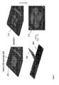
- Figure 4 shows an embodiment and process view of a stacked package substrate with molding, circuit creation and metallization processing
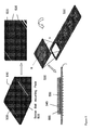
- Figure 5 shows an embodiment and process view of a stacked package substrate with solder ball attachment and singulation for an un-stacked configuration with a ball grid array
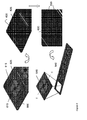
- Figure 6 shows an embodiment and process view of a stacked package substrate with solder ball attachment and singulation for a pre-stacked configuration with a ball grid array
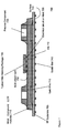
- Figure 7 shows a cross-sectional view of an embodiment of a stacked package with a pre-stacked configuration with a ball grid array
- Figure 8 shows a cross-sectional view of an embodiment of a stacked package with a pre-stacked flip-chip configuration with a ball grid array
- Figure 9 is an example flowchart for manufacturing a stacked package using laser direct structuring in an un-stacked configuration.
- Figure 10 is an example flowchart for manufacturing a stacked package using laser direct structuring in a pre-stacked configuration.
- Figure 1 shows an embodiment of a stacked package 100 using laser direct structuring (LDS).
- the stacked package 100 may include a substrate 105 that has a die 110 attached to one surface and solder balls 125 mounted on another surface.
- the die 110 may be encapsulated with molded interconnect device (MID) molding material 115.
- MID molded interconnect device
- the MID molding material 115 may be a laser direct structuring mold material.
- Circuit traces 120 are created on the MID molding material 115.
- a second package 130 may be mounted to the circuit traces 120 using a number of available techniques as described herein.
- Figure 1 shows the second package 130 connected via solder balls 135.
- the circuit traces 120 provide a connection path between the second package 130 and the substrate 105.
- a MID part is an injection molded thermoplastic part with integrated circuit traces using high temperature thermoplastics and structured metallization.
- the MID technology combines plastic components and circuitry in one part through selective metallization and may be implemented using LDS or two shot molding processes.
- the LDS process may use a thermoplastic material, doped with a metal-plastic additive activated by means of laser.
- a mold is created and a laser then writes the circuit trace on the plastic where the laser beam hits the plastic and the metal additive forms a micro-rough track.
- the metal particles of this track form the nuclei for the subsequent metallization.
- Plating with nickel and gold may be done in this manner.
- the LDS process nominally has a wide range of materials, full three-dimensionality in a sphere, and flexibility for changed routing of traces by the laser unit. Different functional components may be produced from one basic unit and fine traces with a diameter of ⁇ 80 microns are possible.
- the LDS process nominally uses one shot injection molding of commercially available doped thermo-plastic.
- the laser-activatable thermoplastic is doped with a special additive that is activated by the laser beam.
- a physical chemical reaction forms metallic nuclei. These act as a catalyst for reductive copper plating.
- the laser creates a microscopically rough surface in which the copper is firmly anchored during metallization.
- Metallization of the LDS parts, i.e., the circuitry is next.
- An additive build-up of the traces typically up to 5 to 8 um with electro-less copper baths, is followed by plating with nickel and gold.
- the stacked package using LDS provides the ability to do package on package stacking and results in an effective 3D integration of devices.
- stacked packaging using LDS may enable the stacking of high density logic devices and memory devices together.
- This vertical packaging integration is implemented using MID technology applied to packaging and in particular, by using MID molding material for the transfer molding process.
- miniaturization may be achieved due to the highly integrated packages. This results in a small form factor product with a small footprint.
- the stacked package may reduce main printed circuit board real estate area and may provide shorter interconnections for faster data transfer rate.
- Figures 2A, 2B and 2C show different sections and views of an embodiment of a stacked package using laser direct structuring.
- Figure 2A shows a substrate 205 that has a die 210 attached to one surface and solder balls 225 mounted on another surface. That is, the package platform may be a land grid array (LGA), ball grid array (BGA), plastic ball grid array (PBGA) or the like.
- the die 210 may be encapsulated with a LDS molding material 215. After encapsulating the die 210 with the LDS molding material 215, a surface of the LDS molding material 215 may be activated using 3D laser beams and plated with Ni/Au plating to create circuit traces 220 on the LDS molding material 215.
- the circuit traces may connect the top and side surfaces of the LDS molding material 215 with the substrate 205.
- Figure 2B shows a cross-sectional view taken along line A-A of the embodiment shown in Figure 2A .
- the circuit traces 220 may establish multiple connections paths to the substrate 205 along a top surface and side surfaces of the LDS molding material 215.
- Figure 2C shows a package 230 that may be stacked on the circuit traces 220.
- the package 230 may be any type of package and may include flip chip packages, chip scale packages, wire bonding packages, lead frame packages, surface mounted passives, passive components, active components and the like, by way of non-limiting examples.
- Figures 3-7 show an embodiment and process flow for a stacked package using LDS.
- Figure 3 shows a substrate strip 300 that may have multiple substrate units 305.
- the substrate may be flexible tape, ceramics, lead frame, rigid substrate such as bis-maleimide triazine (BT) or FR4 material and the like.
- Each substrate unit 305 may have a top surface 310 and a bottom surface 315.
- Each substrate unit 305 may further have wire bonding pads 320 on the top surface 310, by way of non-limiting example.
- the wire bonding pads 320 may be arranged in a rectangular format to form a die attach section 330.
- the bottom surface 310 may have solder ball mounting pads 335, by way of non-limiting example.
- a protective film 340 may be attached to the bottom surface 310 to protect the solder ball mounting pads 335 from further processing. Attachment of the protective film is done at the substrate strip level.
- a die 345 may be placed and wire bond attached to the die attach section 330 in each substrate unit 305 using wires 350.
- Other techniques such as flip-chip bonding techniques and processes known to those of skill in the art may also be used. These may include, by way of non-limiting example only, thermo-compression or thermo-sonic flip chip bonding techniques. Die attachment is done at the substrate strip level.
- Figure 4 shows an embodiment and process view of a stacked package substrate with molding, circuit creation and metallization processing.
- Figure 4 shows a substrate unit 400 having an attached die (not visible) that is covered with a mold 405.
- the mold 405 may be implemented using mold transfer techniques and processes known to those of skill in the art.
- the mold may be a LDS mold or other MID mold material. The mold transfer may be done at the strip level to increase efficiencies and decrease costs.
- the mold 405 may then be activated by using a laser to create circuitry 410 on the surface of the mold 405.
- Metallization processing may then be applied to the circuitry 410 to create plated circuit traces 415.
- the substrate unit 400 may then be flipped over and a protective film 420 may be removed from a bottom surface 425.
- Figure 5 shows an embodiment and process view of a stacked package substrate with solder ball attachment and singulation for an un-stacked configuration with a ball grid array.
- Figure 5 shows solder ball mounting pads 505 on a bottom surface 510 of a substrate unit 500.
- Solder balls 520 are attached to the solder ball mounting pads 505 to create a ball grid array 525 using solder ball attachment and reflow techniques and processes known to those of skill in the art.
- Singulation may then by used to separate an unstacked BGA substrate unit 535 from an unstacked BGA substrate strip 530. Singulation may be done using techniques and processes known to those of skill in the art.
- a cross-sectional view of the unstacked BGA substrate unit 535 taken along line B-B shows a substrate 540 with a wire bonded 545 die 550.
- the die 550 is encapsulated with a metalized circuit (not visible) mold material 555.
- the unstacked BGA substrate unit 525 may then be sent to an electronic manufacturing service (EMS) to have surface mounted components (SMTs) mounted on the BGA 525 and/or on the metalized circuit mold material 555.
- EMS electronic manufacturing service
- SMTs surface mounted components
- Another package as described herein above may also be attached to the metalized circuit mold material 555.
- Stacked package using LDS may provide a flexible design since this can work with most packages and work with different package suppliers. It may lead to faster times to market and non-recurring engineering (NRE) tooling may be minimal since this may only require a change to the laser programming.
- NRE non-recurring engineering
- the ability to fully test packages eliminates the known good die (KGD) issue due to die yields. Added flexibility includes having the choice of pre-stacked packages on the component level or un-stacked packages for the EMS to do the final stacking during the board assembly.
- the stacked package using LDS may improve logistics, provide procurement flexibility, and maintain confidential or proprietary information.
- Figure 6 shows an embodiment and process view of a stacked package substrate with solder ball attachment and singulation for a pre-stacked configuration with a ball grid array.
- Figure 6 shows a pre-stacked substrate unit 605 of a pre-stacked substrate strip 600, where a package 610 is attached to a metalized circuit mold material 615.
- the package 610 may be attached using flip-chip bonding techniques and processes known to those of skill in the art. These may include, by way of non-limiting example only, thermo-compression or thermo-sonic flip chip bonding techniques as well as flip chip bonding with conductive epoxy and flip chip bonding using anisotropic conductive paste (ACP).
- ACP anisotropic conductive paste
- a bottom surface 620 of the pre-stacked substrate strip 600 may include solder ball mounting pads 625. As described hereinabove, solder balls 630 are attached to the solder ball mounting pads 625 to create a ball grid array 635 using solder ball attachment and reflow techniques and processes known to those of skill in the art. Singulation may then be used to separate a pre-stacked BGA substrate unit 645 from a pre-stacked BGA substrate strip 640. Singulation may be done using techniques and processes known to those of skill in the art.
- FIG. 7 shows a cross-sectional view of a pre-stacked BGA substrate unit 700 taken along line C-C in Figure 6 .
- Pre-stacked BGA substrate unit 700 includes a substrate 705 having a die 710 wire bond attached with wire 715.
- Wire 715 may be gold wire.
- the die 710 may be encapsulated with a mold material 715 having a metalized circuit 720.
- a package 725 may be attached or mounted on the metalized circuit 720 using BGA attachment 730 techniques and processes known to those of skill in the art.
- the package 725 by way of non-limiting example, may be a wire bonded package.
- SMTs 735 may be attached or mounted on the metalized circuit 720 using techniques and processes known to those of skill in the art.
- a bottom surface 740 of the pre-stacked substrate unit 700 may include solder balls 745 to form a ball grid array.
- FIG 8 shows a cross-sectional view of a pre-stacked flip chip BGA substrate unit 800.
- Pre-stacked flip chip BGA substrate unit 800 includes a substrate 805 having a die 810 wire bond attached with wire 813.
- Wire 813 may be gold wire.
- the die 810 may be encapsulated with a mold material 815 having a metalized circuit 820.
- a package 825 may be attached or mounted on the metalized circuit 820 using flip chip attachment techniques and processes known to those of skill in the art and described hereinabove.
- SMTs 835 may be attached or mounted on the metalized circuit 820 using techniques and processes known to those of skill in the art.
- a bottom surface 840 of the pre-stacked substrate unit 800 may include solder balls 845 to form a ball grid array.
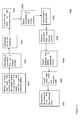
- Figure 9 is an example flowchart 900 for manufacturing a stacked package using laser direct structuring in an un-stacked configuration.
- a substrate may be processed to include wire bonding pads and a die attach section on a top surface and solder ball mounting pads on a bottom surface (910).
- a protective film may be attached to bottom surface (915).
- a die is attached to the substrate as described hereinabove (920).
- the die may be encapsulated with LDS mold material (925).
- the mold material is laser activated to create circuitry on the mold material (930).
- the circuitry undergoes metallization (935).
- the protective film is removed from the bottom surface (940). Solder balls are attached to solder ball mounting pads to create BGA (945).
- Each substrate unit is singulated from the substrate strip (950) and is sent to an EMS for package and SMT attachment (955).
- Figure 10 is an example flowchart 1000 for manufacturing a stacked package using laser direct structuring in a pre-stacked configuration.
- a substrate may be processed to include wire bonding pads and a die attach section on a top surface and solder ball mounting pads on a bottom surface (1010).
- a protective film may be attached to bottom surface (1015).
- a die is attached to the substrate as described hereinabove (1020).
- the die may be encapsulated with LDS mold material (1025).
- the mold material is laser activated to create circuitry on the mold material (1030).
- the circuitry undergoes metallization (1035).
- the protective film is removed from the bottom surface (1040).
- a package and/or SMTs are attached to the metalized circuitry on the mold (1045).
- Solder balls are attached to solder ball mounting pads to create BGA (1050).
- Each substrate unit is singulated from the substrate strip (1055).
- the methods described herein are not limited to any particular element(s) that perform(s) any particular function(s) and some steps of the methods presented need not necessarily occur in the order shown. For example, in some cases two or more method steps may occur in a different order or simultaneously. In addition, some steps of the described methods may be optional (even if not explicitly stated to be optional) and, therefore, may be omitted. These and other variations of the methods disclosed herein will be readily apparent, especially in view of the description of the stacked package described herein, and are considered to be within the full scope of the invention.
Landscapes
- Engineering & Computer Science (AREA)
- Microelectronics & Electronic Packaging (AREA)
- Encapsulation Of And Coatings For Semiconductor Or Solid State Devices (AREA)
- Wire Bonding (AREA)
- Manufacturing Of Printed Wiring (AREA)
- Structures For Mounting Electric Components On Printed Circuit Boards (AREA)
- Manufacturing & Machinery (AREA)
- Semiconductor Lasers (AREA)
Abstract
Description
- This application is related to packaging of electronic devices.
- The desire for smaller, compact, cheaper and feature rich electronic devices, such as digital cameras, digital video cameras, phones, music players and the like, drives and forces minimization and efficient use of circuit boards.
- Described herein is a stacked package using laser direct structuring. The stacked package includes a die attached to a substrate. The die is encapsulated with a laser direct structuring mold material. The laser direct structuring mold material is laser activated to form circuit traces on the top and side surfaces of the laser direct structuring mold material. The circuit traces then undergo metallization. A package is then attached to the metalized circuit traces and is electrically connected to the substrate via the metalized circuit traces.
- In accordance with a first aspect of the present invention, a method for manufacturing a stacked package using laser direct structuring (LDS), comprises:
- preparing a substrate strip with at least one die;
- encapsulating each die with LDS mold material;
- laser activating at least one surface of the LDS mold material on the at least one die to form circuit traces on the LDS mold material;
- metalizing the circuit traces; and
- attaching a package on metalized circuit traces.
- The method may further comprise:
- providing solder ball mounting pads on a surface opposite an attached die.
- The method may further comprise:
- attaching solder balls to the solder ball mounting pads to form a ball grid array.
- The method may further comprise:
- attaching a protective film to a surface opposite an attached die that protects solder ball mounting pads.
- The method may further comprise:
- singulating a substrate unit from the substrate strip after metallization of the circuit traces.
- The method may further comprise:
- singulating a substrate unit from the substrate strip.
- The method may further comprise:
- attaching components to the metalized circuit traces.
- The package may be attached using one of flip chip attachment or ball grid array attachment.
- In accordance with a second aspect of the present invention, a laser direct structuring (LDS) stacked package comprises:
- a substrate;
- a LDS mold material covered die attached to the substrate, wherein at least one surface of the LDS mold material has metalized circuit traces; and
- a package attached to the metalized circuit traces.
- The LDS stacked package may further comprise:
- solder ball mounting pads on a surface opposite an attached die.
- The LDS stacked package may further comprise:
- a ball grid array on a surface opposite an attached die.
- The LDS stacked package may further comprise:
- components attached to the metalized circuit traces.
- The package may be attached using one of flip chip attachment or ball grid array attachment.
- The present invention further provides an electronic device, comprising:
- a substrate having a top surface and a bottom surface;
- a laser direct structuring (LDS) mold material covered die attached to the top surface of the substrate, wherein at least one surface of the LDS mold material has metalized circuit traces; and
- a package attached to the metalized circuit traces.
- The electronic device may further comprise:
- components attached to the metalized circuit traces.
-
Figure 1 shows an embodiment of a stacked package using laser direct structuring; -
Figures 2A, 2B and 2C show different sections and views of an embodiment of a stacked package using laser direct structuring; -
Figure 3 shows an embodiment and process view of a stacked package substrate with die bond and wire bond processing; -
Figure 4 shows an embodiment and process view of a stacked package substrate with molding, circuit creation and metallization processing; -
Figure 5 shows an embodiment and process view of a stacked package substrate with solder ball attachment and singulation for an un-stacked configuration with a ball grid array; -
Figure 6 shows an embodiment and process view of a stacked package substrate with solder ball attachment and singulation for a pre-stacked configuration with a ball grid array; -
Figure 7 shows a cross-sectional view of an embodiment of a stacked package with a pre-stacked configuration with a ball grid array; -
Figure 8 shows a cross-sectional view of an embodiment of a stacked package with a pre-stacked flip-chip configuration with a ball grid array; -
Figure 9 is an example flowchart for manufacturing a stacked package using laser direct structuring in an un-stacked configuration; and -
Figure 10 is an example flowchart for manufacturing a stacked package using laser direct structuring in a pre-stacked configuration. - It is to be understood that the figures and descriptions of embodiments of the stacked package using laser direct structuring have been simplified to illustrate elements that are relevant for a clear understanding, while eliminating, for the purpose of clarity, many other elements found in typical electronics packaging. Those of ordinary skill in the art may recognize that other elements and/or steps are desirable and/or required in implementing the present invention. However, because such elements and steps are well known in the art, and because they do not facilitate a better understanding of the present invention, a discussion of such elements and steps is not provided herein.
- The non-limiting embodiments described herein are with respect to electronic devices. Other devices, modules and applications may also be used in view of these teachings without deviating from the spirit or scope as described herein. The stacked package using laser direct structuring may be modified for a variety of applications and uses while remaining within the spirit and scope of the claims. The embodiments and variations described herein, and/or shown in the drawings, are presented by way of example only and are not limiting as to the scope and spirit. The descriptions herein may be applicable to all embodiments of the stacked package using laser direct structuring although it may be described with respect to a particular embodiment.
- In general,
Figure 1 shows an embodiment of astacked package 100 using laser direct structuring (LDS). Thestacked package 100 may include asubstrate 105 that has a die 110 attached to one surface andsolder balls 125 mounted on another surface. Thedie 110 may be encapsulated with molded interconnect device (MID)molding material 115. By way of non-limiting example, theMID molding material 115 may be a laser direct structuring mold material. Circuit traces 120 are created on theMID molding material 115. Asecond package 130 may be mounted to the circuit traces 120 using a number of available techniques as described herein. By way of non-limiting example,Figure 1 shows thesecond package 130 connected viasolder balls 135. The circuit traces 120 provide a connection path between thesecond package 130 and thesubstrate 105. - A MID part is an injection molded thermoplastic part with integrated circuit traces using high temperature thermoplastics and structured metallization. The MID technology combines plastic components and circuitry in one part through selective metallization and may be implemented using LDS or two shot molding processes.
- In general, the LDS process may use a thermoplastic material, doped with a metal-plastic additive activated by means of laser. A mold is created and a laser then writes the circuit trace on the plastic where the laser beam hits the plastic and the metal additive forms a micro-rough track. The metal particles of this track form the nuclei for the subsequent metallization. In an electro-less copper bath the conductor path layers arise precisely on these tracks. Plating with nickel and gold may be done in this manner. The LDS process nominally has a wide range of materials, full three-dimensionality in a sphere, and flexibility for changed routing of traces by the laser unit. Different functional components may be produced from one basic unit and fine traces with a diameter of <80 microns are possible.
- Procedurally, in one embodiment, the LDS process nominally uses one shot injection molding of commercially available doped thermo-plastic. The laser-activatable thermoplastic is doped with a special additive that is activated by the laser beam. A physical chemical reaction forms metallic nuclei. These act as a catalyst for reductive copper plating. In addition to the activation, the laser creates a microscopically rough surface in which the copper is firmly anchored during metallization. Metallization of the LDS parts, i.e., the circuitry, is next. An additive build-up of the traces, typically up to 5 to 8 um with electro-less copper baths, is followed by plating with nickel and gold.
- As illustrated in
Figure 1 , the stacked package using LDS provides the ability to do package on package stacking and results in an effective 3D integration of devices. In a non-limiting example, stacked packaging using LDS may enable the stacking of high density logic devices and memory devices together. This vertical packaging integration is implemented using MID technology applied to packaging and in particular, by using MID molding material for the transfer molding process. Moreover, miniaturization may be achieved due to the highly integrated packages. This results in a small form factor product with a small footprint. The stacked package may reduce main printed circuit board real estate area and may provide shorter interconnections for faster data transfer rate. -
Figures 2A, 2B and 2C show different sections and views of an embodiment of a stacked package using laser direct structuring.Figure 2A shows asubstrate 205 that has a die 210 attached to one surface andsolder balls 225 mounted on another surface. That is, the package platform may be a land grid array (LGA), ball grid array (BGA), plastic ball grid array (PBGA) or the like. Thedie 210 may be encapsulated with aLDS molding material 215. After encapsulating thedie 210 with theLDS molding material 215, a surface of theLDS molding material 215 may be activated using 3D laser beams and plated with Ni/Au plating to create circuit traces 220 on theLDS molding material 215. The circuit traces may connect the top and side surfaces of theLDS molding material 215 with thesubstrate 205.Figure 2B shows a cross-sectional view taken along line A-A of the embodiment shown inFigure 2A . As illustrated, the circuit traces 220 may establish multiple connections paths to thesubstrate 205 along a top surface and side surfaces of theLDS molding material 215. -
Figure 2C shows apackage 230 that may be stacked on the circuit traces 220. Thepackage 230 may be any type of package and may include flip chip packages, chip scale packages, wire bonding packages, lead frame packages, surface mounted passives, passive components, active components and the like, by way of non-limiting examples. -
Figures 3-7 show an embodiment and process flow for a stacked package using LDS.Figure 3 shows asubstrate strip 300 that may havemultiple substrate units 305. The substrate may be flexible tape, ceramics, lead frame, rigid substrate such as bis-maleimide triazine (BT) or FR4 material and the like. Eachsubstrate unit 305 may have atop surface 310 and abottom surface 315. Eachsubstrate unit 305 may further havewire bonding pads 320 on thetop surface 310, by way of non-limiting example. Thewire bonding pads 320 may be arranged in a rectangular format to form a die attachsection 330. Thebottom surface 310 may have solderball mounting pads 335, by way of non-limiting example. Aprotective film 340 may be attached to thebottom surface 310 to protect the solderball mounting pads 335 from further processing. Attachment of the protective film is done at the substrate strip level. - A
die 345 may be placed and wire bond attached to the die attachsection 330 in eachsubstrate unit 305 usingwires 350. Other techniques such as flip-chip bonding techniques and processes known to those of skill in the art may also be used. These may include, by way of non-limiting example only, thermo-compression or thermo-sonic flip chip bonding techniques. Die attachment is done at the substrate strip level. -
Figure 4 shows an embodiment and process view of a stacked package substrate with molding, circuit creation and metallization processing.Figure 4 shows asubstrate unit 400 having an attached die (not visible) that is covered with amold 405. Themold 405 may be implemented using mold transfer techniques and processes known to those of skill in the art. The mold may be a LDS mold or other MID mold material. The mold transfer may be done at the strip level to increase efficiencies and decrease costs. - The
mold 405 may then be activated by using a laser to createcircuitry 410 on the surface of themold 405. Metallization processing may then be applied to thecircuitry 410 to create plated circuit traces 415. Thesubstrate unit 400 may then be flipped over and aprotective film 420 may be removed from abottom surface 425. -
Figure 5 shows an embodiment and process view of a stacked package substrate with solder ball attachment and singulation for an un-stacked configuration with a ball grid array.Figure 5 shows solderball mounting pads 505 on abottom surface 510 of asubstrate unit 500.Solder balls 520 are attached to the solderball mounting pads 505 to create aball grid array 525 using solder ball attachment and reflow techniques and processes known to those of skill in the art. Singulation may then by used to separate an unstackedBGA substrate unit 535 from an unstackedBGA substrate strip 530. Singulation may be done using techniques and processes known to those of skill in the art. - A cross-sectional view of the unstacked
BGA substrate unit 535 taken along line B-B shows a substrate 540 with a wire bonded 545die 550. Thedie 550 is encapsulated with a metalized circuit (not visible)mold material 555. The unstackedBGA substrate unit 525 may then be sent to an electronic manufacturing service (EMS) to have surface mounted components (SMTs) mounted on theBGA 525 and/or on the metalizedcircuit mold material 555. Another package as described herein above may also be attached to the metalizedcircuit mold material 555. - Stacked package using LDS may provide a flexible design since this can work with most packages and work with different package suppliers. It may lead to faster times to market and non-recurring engineering (NRE) tooling may be minimal since this may only require a change to the laser programming. The ability to fully test packages eliminates the known good die (KGD) issue due to die yields. Added flexibility includes having the choice of pre-stacked packages on the component level or un-stacked packages for the EMS to do the final stacking during the board assembly. The stacked package using LDS may improve logistics, provide procurement flexibility, and maintain confidential or proprietary information.
-
Figure 6 shows an embodiment and process view of a stacked package substrate with solder ball attachment and singulation for a pre-stacked configuration with a ball grid array.Figure 6 shows apre-stacked substrate unit 605 of apre-stacked substrate strip 600, where apackage 610 is attached to a metalizedcircuit mold material 615. Thepackage 610 may be attached using flip-chip bonding techniques and processes known to those of skill in the art. These may include, by way of non-limiting example only, thermo-compression or thermo-sonic flip chip bonding techniques as well as flip chip bonding with conductive epoxy and flip chip bonding using anisotropic conductive paste (ACP). - A
bottom surface 620 of thepre-stacked substrate strip 600 may include solderball mounting pads 625. As described hereinabove,solder balls 630 are attached to the solderball mounting pads 625 to create aball grid array 635 using solder ball attachment and reflow techniques and processes known to those of skill in the art. Singulation may then be used to separate a pre-stackedBGA substrate unit 645 from a pre-stackedBGA substrate strip 640. Singulation may be done using techniques and processes known to those of skill in the art. -
Figure 7 shows a cross-sectional view of a pre-stackedBGA substrate unit 700 taken along line C-C inFigure 6 . Pre-stackedBGA substrate unit 700 includes asubstrate 705 having a die 710 wire bond attached withwire 715.Wire 715, by way of non-limiting example, may be gold wire. Thedie 710 may be encapsulated with amold material 715 having a metalizedcircuit 720. Apackage 725 may be attached or mounted on the metalizedcircuit 720 usingBGA attachment 730 techniques and processes known to those of skill in the art. Thepackage 725, by way of non-limiting example, may be a wire bonded package.SMTs 735 may be attached or mounted on the metalizedcircuit 720 using techniques and processes known to those of skill in the art. Abottom surface 740 of thepre-stacked substrate unit 700 may includesolder balls 745 to form a ball grid array. -
Figure 8 shows a cross-sectional view of a pre-stacked flip chipBGA substrate unit 800. Pre-stacked flip chipBGA substrate unit 800 includes asubstrate 805 having a die 810 wire bond attached withwire 813.Wire 813, by way of non-limiting example, may be gold wire. The die 810 may be encapsulated with amold material 815 having a metalizedcircuit 820. Apackage 825 may be attached or mounted on the metalizedcircuit 820 using flip chip attachment techniques and processes known to those of skill in the art and described hereinabove.SMTs 835 may be attached or mounted on the metalizedcircuit 820 using techniques and processes known to those of skill in the art. Abottom surface 840 of thepre-stacked substrate unit 800 may includesolder balls 845 to form a ball grid array. -
Figure 9 is anexample flowchart 900 for manufacturing a stacked package using laser direct structuring in an un-stacked configuration. A substrate may be processed to include wire bonding pads and a die attach section on a top surface and solder ball mounting pads on a bottom surface (910). A protective film may be attached to bottom surface (915). A die is attached to the substrate as described hereinabove (920). The die may be encapsulated with LDS mold material (925). The mold material is laser activated to create circuitry on the mold material (930). The circuitry undergoes metallization (935). The protective film is removed from the bottom surface (940). Solder balls are attached to solder ball mounting pads to create BGA (945). Each substrate unit is singulated from the substrate strip (950) and is sent to an EMS for package and SMT attachment (955). -
Figure 10 is anexample flowchart 1000 for manufacturing a stacked package using laser direct structuring in a pre-stacked configuration. A substrate may be processed to include wire bonding pads and a die attach section on a top surface and solder ball mounting pads on a bottom surface (1010). A protective film may be attached to bottom surface (1015). A die is attached to the substrate as described hereinabove (1020). The die may be encapsulated with LDS mold material (1025). The mold material is laser activated to create circuitry on the mold material (1030). The circuitry undergoes metallization (1035). The protective film is removed from the bottom surface (1040). A package and/or SMTs are attached to the metalized circuitry on the mold (1045). Solder balls are attached to solder ball mounting pads to create BGA (1050). Each substrate unit is singulated from the substrate strip (1055). - As described herein, the methods described herein are not limited to any particular element(s) that perform(s) any particular function(s) and some steps of the methods presented need not necessarily occur in the order shown. For example, in some cases two or more method steps may occur in a different order or simultaneously. In addition, some steps of the described methods may be optional (even if not explicitly stated to be optional) and, therefore, may be omitted. These and other variations of the methods disclosed herein will be readily apparent, especially in view of the description of the stacked package described herein, and are considered to be within the full scope of the invention.
- Although features and elements are described above in particular combinations, each feature or element can be used alone without the other features and elements or in various combinations with or without other features and elements.
Claims (15)
- A method for manufacturing a stacked package using laser direct structuring (LDS), comprising:preparing a substrate strip with at least one die;encapsulating each die with LDS mold material;laser activating at least one surface of the LDS mold material on the at least one die to form circuit traces on the LDS mold material;metalizing the circuit traces; andattaching a package on metalized circuit traces.
- The method of claim 1, further comprising:providing solder ball mounting pads on a surface opposite an attached die.
- The method of claim 2, further comprising:attaching solder balls to the solder ball mounting pads to form a ball grid array.
- The method of any of the preceding claims, further comprising:attaching a protective film to a surface opposite an attached die that protects solder ball mounting pads.
- The method of any of the preceding claims, further comprising:singulating a substrate unit from the substrate strip after metallization of the circuit traces.
- The method of any of the preceding claims, further comprising:singulating a substrate unit from the substrate strip.
- The method of any of the preceding claims, further comprising:attaching components to the metalized circuit traces.
- The method of any of the preceding claims, wherein the package is attached using one of flip chip attachment or ball grid array attachment.
- A laser direct structuring (LDS) stacked package, comprising:a substrate;a LDS mold material covered die attached to the substrate, wherein at least one surface of the LDS mold material has metalized circuit traces; anda package attached to the metalized circuit traces.
- The LDS stacked package of claim 9, further comprising:solder ball mounting pads on a surface opposite an attached die.
- The LDS stacked package of claim 9 or claim 10, further comprising:a ball grid array on a surface opposite an attached die.
- The LDS stacked package of any of claims 9 to 11, further comprising:components attached to the metalized circuit traces.
- The LDS stacked package of any of claims 9 to 12, wherein the package is attached using one of flip chip attachment or ball grid array attachment.
- An electronic device, comprising:a substrate having a top surface and a bottom surface;a laser direct structuring (LDS) mold material covered die attached to the top surface of the substrate, wherein at least one surface of the LDS mold material has metalized circuit traces; anda package attached to the metalized circuit traces.
- The electronic device of claim 14, further comprising:components attached to the metalized circuit traces.
Applications Claiming Priority (1)
| Application Number | Priority Date | Filing Date | Title |
|---|---|---|---|
| US13/286,366 US8642387B2 (en) | 2011-11-01 | 2011-11-01 | Method of fabricating stacked packages using laser direct structuring |
Publications (2)
| Publication Number | Publication Date |
|---|---|
| EP2590217A2 true EP2590217A2 (en) | 2013-05-08 |
| EP2590217A3 EP2590217A3 (en) | 2015-09-30 |
Family
ID=47257449
Family Applications (1)
| Application Number | Title | Priority Date | Filing Date |
|---|---|---|---|
| EP12190418.9A Ceased EP2590217A3 (en) | 2011-11-01 | 2012-10-29 | Stacked packages using laser direct structuring |
Country Status (4)
| Country | Link |
|---|---|
| US (2) | US8642387B2 (en) |
| EP (1) | EP2590217A3 (en) |
| CN (1) | CN103094131B (en) |
| MX (1) | MX2012012713A (en) |
Cited By (3)
| Publication number | Priority date | Publication date | Assignee | Title |
|---|---|---|---|---|
| EP2869309A1 (en) * | 2013-11-01 | 2015-05-06 | Industrial Technology Research Institute | Method for forming metal circuit, liquid trigger material for forming metal circuit and metal circuit structure |
| EP3351063A4 (en) * | 2015-09-16 | 2018-10-17 | Jabil Inc. | System, apparatus and method for utilizing surface mount technology on plastic substrates |
| DE102020112879A1 (en) | 2020-05-12 | 2021-11-18 | Lpkf Laser & Electronics Aktiengesellschaft | Composite structure with at least one electronic component and a method for producing such a composite structure |
Families Citing this family (14)
| Publication number | Priority date | Publication date | Assignee | Title |
|---|---|---|---|---|
| US8642387B2 (en) | 2011-11-01 | 2014-02-04 | Flextronics Ap, Llc | Method of fabricating stacked packages using laser direct structuring |
| CN103530673A (en) * | 2013-07-25 | 2014-01-22 | 上海杉德金卡信息系统科技有限公司 | Finance PCI safety design method based on LDS technology |
| KR102147354B1 (en) | 2013-11-14 | 2020-08-24 | 삼성전자 주식회사 | Semiconductor package and method for manufacturing the same |
| KR102245003B1 (en) | 2014-06-27 | 2021-04-28 | 삼성전자주식회사 | Semiconductor packages capable of overcoming overhangs and methods for fabricating the same |
| DE202014008843U1 (en) * | 2014-11-06 | 2014-11-24 | Rosenberger Hochfrequenztechnik Gmbh & Co. Kg | Printed circuit board assembly |
| CN105140191B (en) * | 2015-09-17 | 2019-03-01 | 中芯长电半导体(江阴)有限公司 | A kind of packaging structure and method of making redistribution lead layer |
| JP6691835B2 (en) * | 2016-06-17 | 2020-05-13 | 株式会社アムコー・テクノロジー・ジャパン | Method for manufacturing semiconductor package |
| IT201700055983A1 (en) | 2017-05-23 | 2018-11-23 | St Microelectronics Srl | PROCEDURE FOR PRODUCING SEMICONDUCTOR, SEMICONDUCTOR AND CORRESPONDENT CIRCUIT DEVICES |
| CN107256847A (en) * | 2017-05-27 | 2017-10-17 | 华天科技(昆山)电子有限公司 | Increase chip-packaging structure of bonding pad area and preparation method thereof |
| TWI616999B (en) * | 2017-07-20 | 2018-03-01 | Atp Electronics Taiwan Inc. | Memory manufacturing method with stacked integrated circuit chip |
| US11302613B2 (en) | 2019-07-17 | 2022-04-12 | Infineon Technologies Ag | Double-sided cooled molded semiconductor package |
| US10886199B1 (en) * | 2019-07-17 | 2021-01-05 | Infineon Technologies Ag | Molded semiconductor package with double-sided cooling |
| CN113078118A (en) * | 2021-03-25 | 2021-07-06 | 福唐激光(苏州)科技有限公司 | Method for realizing POP (point of presence protocol) connection by laser and POP structure thereof |
| US12599004B2 (en) | 2022-09-28 | 2026-04-07 | Nxp Usa, Inc. | Semiconductor device with active mold package and method therefor |
Citations (1)
| Publication number | Priority date | Publication date | Assignee | Title |
|---|---|---|---|---|
| US20080169539A1 (en) * | 2007-01-12 | 2008-07-17 | Silicon Storage Tech., Inc. | Under bump metallurgy structure of a package and method of making same |
Family Cites Families (10)
| Publication number | Priority date | Publication date | Assignee | Title |
|---|---|---|---|---|
| CN1157790C (en) * | 2000-11-27 | 2004-07-14 | 矽品精密工业股份有限公司 | Chip stacking and packaging structure |
| US7633765B1 (en) * | 2004-03-23 | 2009-12-15 | Amkor Technology, Inc. | Semiconductor package including a top-surface metal layer for implementing circuit features |
| US7548430B1 (en) * | 2002-05-01 | 2009-06-16 | Amkor Technology, Inc. | Buildup dielectric and metallization process and semiconductor package |
| DE102004049654B3 (en) * | 2004-10-11 | 2006-04-13 | Infineon Technologies Ag | Semiconductor device with plastic housing and method for producing the same |
| DE102004049663B3 (en) * | 2004-10-11 | 2006-04-13 | Infineon Technologies Ag | Plastic housing and semiconductor device with such plastic housing and method for producing the same |
| DE102005006995B4 (en) * | 2005-02-15 | 2008-01-24 | Infineon Technologies Ag | Semiconductor device with plastic housing and external connections and method for producing the same |
| KR101187214B1 (en) * | 2009-03-13 | 2012-10-02 | 테세라, 인코포레이티드 | Stacked microelectronic assembly with microelectronic elements having vias extending through bond pads |
| EP2309535A1 (en) * | 2009-10-09 | 2011-04-13 | Telefonaktiebolaget L M Ericsson (Publ) | Chip package with a chip embedded in a wiring body |
| US8354297B2 (en) * | 2010-09-03 | 2013-01-15 | Stats Chippac, Ltd. | Semiconductor device and method of forming different height conductive pillars to electrically interconnect stacked laterally offset semiconductor die |
| US8642387B2 (en) * | 2011-11-01 | 2014-02-04 | Flextronics Ap, Llc | Method of fabricating stacked packages using laser direct structuring |
-
2011
- 2011-11-01 US US13/286,366 patent/US8642387B2/en not_active Expired - Fee Related
-
2012
- 2012-10-29 EP EP12190418.9A patent/EP2590217A3/en not_active Ceased
- 2012-10-31 MX MX2012012713A patent/MX2012012713A/en active IP Right Grant
- 2012-11-01 CN CN201210431122.7A patent/CN103094131B/en not_active Expired - Fee Related
-
2014
- 2014-01-02 US US14/146,376 patent/US9018749B2/en active Active
Patent Citations (1)
| Publication number | Priority date | Publication date | Assignee | Title |
|---|---|---|---|---|
| US20080169539A1 (en) * | 2007-01-12 | 2008-07-17 | Silicon Storage Tech., Inc. | Under bump metallurgy structure of a package and method of making same |
Non-Patent Citations (4)
| Title |
|---|
| ANONYMOUS: "Electroless plating - Wikipedia", 9 February 2019 (2019-02-09), XP055581150, Retrieved from the Internet <URL:https://en.wikipedia.org/wiki/Electroless_plating> [retrieved on 20190415] * |
| ANONYMOUS: "MIDs Make A Comeback | Plastics Technology", 1 June 2005 (2005-06-01), XP055782422, Retrieved from the Internet <URL:https://www.ptonline.com/articles/mids-make-a-comeback> [retrieved on 20210305] * |
| ANONYMOUS: "Molded interconnect device - Wikipedia, the free encyclopedia", 9 February 2015 (2015-02-09), XP055290225, Retrieved from the Internet <URL:https://en.wikipedia.org/w/index.php?title=Molded_interconnect_device&oldid=646412742> [retrieved on 20160721] * |
| LPKF: "Three-Dimensional Circuits LPKF LDS: Laser Direct Structuring for 3D Molded Interconnect Devices 2 Innovative Product Design with MID Technology Contents 2 More Functionality - New Possibilities 4 Flexible Solution for Three-Dimensional Circuits 6 Tomorrow's Technology in Today's Production 8 Inspir", 4 August 2014 (2014-08-04), XP055645749, Retrieved from the Internet <URL:https://www.lpkf.com/fileadmin/mediafiles/user_upload/products/pdf/EQ/3D-MID-LDS/brochure_lpkf_laser_direct_structuring_en.pdf> [retrieved on 20191122] * |
Cited By (7)
| Publication number | Priority date | Publication date | Assignee | Title |
|---|---|---|---|---|
| EP2869309A1 (en) * | 2013-11-01 | 2015-05-06 | Industrial Technology Research Institute | Method for forming metal circuit, liquid trigger material for forming metal circuit and metal circuit structure |
| US9499911B2 (en) | 2013-11-01 | 2016-11-22 | Industrial Technology Research Institute | Method for forming metal circuit, liquid trigger material for forming metal circuit and metal circuit structure |
| US9683292B2 (en) | 2013-11-01 | 2017-06-20 | Industrial Technology Research Institute | Metal circuit structure |
| EP3351063A4 (en) * | 2015-09-16 | 2018-10-17 | Jabil Inc. | System, apparatus and method for utilizing surface mount technology on plastic substrates |
| EP4319511A2 (en) | 2015-09-16 | 2024-02-07 | Jabil, Inc. | System, apparatus and method for utilizing surface mount technology on plastic substrates |
| EP4319511A3 (en) * | 2015-09-16 | 2024-04-03 | Jabil, Inc. | System, apparatus and method for utilizing surface mount technology on plastic substrates |
| DE102020112879A1 (en) | 2020-05-12 | 2021-11-18 | Lpkf Laser & Electronics Aktiengesellschaft | Composite structure with at least one electronic component and a method for producing such a composite structure |
Also Published As
| Publication number | Publication date |
|---|---|
| US20130105972A1 (en) | 2013-05-02 |
| US8642387B2 (en) | 2014-02-04 |
| US20140110162A1 (en) | 2014-04-24 |
| US9018749B2 (en) | 2015-04-28 |
| CN103094131B (en) | 2018-02-09 |
| MX2012012713A (en) | 2013-05-14 |
| CN103094131A (en) | 2013-05-08 |
| EP2590217A3 (en) | 2015-09-30 |
Similar Documents
| Publication | Publication Date | Title |
|---|---|---|
| US8642387B2 (en) | Method of fabricating stacked packages using laser direct structuring | |
| CN109585430B (en) | Stacked semiconductor package assembly including double-sided redistribution layer | |
| KR101522763B1 (en) | Apparatus and method for a component package | |
| US7170158B2 (en) | Double-sided circuit board and multi-chip package including such a circuit board and method for manufacture | |
| CN102867800B (en) | Functional chip is connected to packaging part to form package on package | |
| US7989269B2 (en) | Semiconductor package with penetrable encapsulant joining semiconductor die and method thereof | |
| JP5661225B2 (en) | Semiconductor device packaging method | |
| US6489676B2 (en) | Semiconductor device having an interconnecting post formed on an interposer within a sealing resin | |
| US20180114786A1 (en) | Method of forming package-on-package structure | |
| US20090315156A1 (en) | Packaged integrated circuit having conformal electromagnetic shields and methods to form the same | |
| JP2002252303A (en) | Flip chip semiconductor device in molded chip scale package and assembling method | |
| US8604610B1 (en) | Flexible power module semiconductor packages | |
| US20120056334A1 (en) | Semiconductor Device and Method of Forming Pre-Molded Substrate to Reduce Warpage During Die Mounting | |
| US6903449B2 (en) | Semiconductor component having chip on board leadframe | |
| KR20020061812A (en) | Ball grid array type multi chip package and stack package | |
| US10896877B1 (en) | System in package with double side mounted board | |
| US8994157B1 (en) | Circuit system in a package | |
| US6476475B1 (en) | Stacked SRAM die package | |
| US20110266673A1 (en) | Integrated circuit package structure and method | |
| US8987881B2 (en) | Hybrid lead frame and ball grid array package | |
| CN117711956B (en) | Integrated Antenna Structure | |
| TWI917773B (en) | Integrated antenna-in-package structure | |
| KR101392765B1 (en) | Semiconductor package and method for fabricating of the same | |
| US20060145313A1 (en) | Semiconductor package device having reduced mounting height and method for manufacturing the same | |
| CN118679558A (en) | Fan-out flip chip semiconductor package |
Legal Events
| Date | Code | Title | Description |
|---|---|---|---|
| PUAI | Public reference made under article 153(3) epc to a published international application that has entered the european phase |
Free format text: ORIGINAL CODE: 0009012 |
|
| AK | Designated contracting states |
Kind code of ref document: A2 Designated state(s): AL AT BE BG CH CY CZ DE DK EE ES FI FR GB GR HR HU IE IS IT LI LT LU LV MC MK MT NL NO PL PT RO RS SE SI SK SM TR |
|
| AX | Request for extension of the european patent |
Extension state: BA ME |
|
| RIC1 | Information provided on ipc code assigned before grant |
Ipc: H01L 25/10 20060101AFI20150421BHEP Ipc: H01L 23/31 20060101ALN20150421BHEP Ipc: H01L 21/56 20060101ALN20150421BHEP Ipc: H01L 23/29 20060101ALI20150421BHEP Ipc: H01L 21/60 20060101ALI20150421BHEP |
|
| PUAL | Search report despatched |
Free format text: ORIGINAL CODE: 0009013 |
|
| AK | Designated contracting states |
Kind code of ref document: A3 Designated state(s): AL AT BE BG CH CY CZ DE DK EE ES FI FR GB GR HR HU IE IS IT LI LT LU LV MC MK MT NL NO PL PT RO RS SE SI SK SM TR |
|
| AX | Request for extension of the european patent |
Extension state: BA ME |
|
| RIC1 | Information provided on ipc code assigned before grant |
Ipc: H01L 25/10 20060101AFI20150824BHEP Ipc: H01L 21/60 20060101ALI20150824BHEP Ipc: H01L 21/56 20060101ALN20150824BHEP Ipc: H01L 23/29 20060101ALI20150824BHEP Ipc: H01L 23/31 20060101ALN20150824BHEP |
|
| 17P | Request for examination filed |
Effective date: 20160330 |
|
| RBV | Designated contracting states (corrected) |
Designated state(s): AL AT BE BG CH CY CZ DE DK EE ES FI FR GB GR HR HU IE IS IT LI LT LU LV MC MK MT NL NO PL PT RO RS SE SI SK SM TR |
|
| STAA | Information on the status of an ep patent application or granted ep patent |
Free format text: STATUS: EXAMINATION IS IN PROGRESS |
|
| 17Q | First examination report despatched |
Effective date: 20190423 |
|
| STAA | Information on the status of an ep patent application or granted ep patent |
Free format text: STATUS: THE APPLICATION HAS BEEN REFUSED |
|
| 18R | Application refused |
Effective date: 20210319 |