EP2590203A2 - Charged particle beam system aperture - Google Patents
Charged particle beam system aperture Download PDFInfo
- Publication number
- EP2590203A2 EP2590203A2 EP12191348.7A EP12191348A EP2590203A2 EP 2590203 A2 EP2590203 A2 EP 2590203A2 EP 12191348 A EP12191348 A EP 12191348A EP 2590203 A2 EP2590203 A2 EP 2590203A2
- Authority
- EP
- European Patent Office
- Prior art keywords
- aperture
- substrate
- cavity
- conductive layer
- hole
- Prior art date
- Legal status (The legal status is an assumption and is not a legal conclusion. Google has not performed a legal analysis and makes no representation as to the accuracy of the status listed.)
- Granted
Links
Images






Classifications
-
- G—PHYSICS
- G21—NUCLEAR PHYSICS; NUCLEAR ENGINEERING
- G21K—HANDLING OF PARTICLES OR IONISING RADIATION NOT OTHERWISE PROVIDED FOR; IRRADIATION DEVICES; GAMMA RAY OR X-RAY MICROSCOPES
- G21K1/00—Arrangements for handling particles or ionising radiation, e.g. focusing or moderating
-
- H—ELECTRICITY
- H01—ELECTRIC ELEMENTS
- H01J—ELECTRIC DISCHARGE TUBES OR DISCHARGE LAMPS
- H01J37/00—Discharge tubes with provision for introducing objects or material to be exposed to the discharge, e.g. for the purpose of examination or processing thereof
- H01J37/02—Details
- H01J37/04—Arrangements of electrodes and associated parts for generating or controlling the discharge, e.g. electron-optical arrangement or ion-optical arrangement
- H01J37/09—Diaphragms; Shields associated with electron or ion-optical arrangements; Compensation of disturbing fields
-
- H—ELECTRICITY
- H01—ELECTRIC ELEMENTS
- H01J—ELECTRIC DISCHARGE TUBES OR DISCHARGE LAMPS
- H01J2237/00—Discharge tubes exposing object to beam, e.g. for analysis treatment, etching, imaging
- H01J2237/04—Means for controlling the discharge
- H01J2237/045—Diaphragms
-
- H—ELECTRICITY
- H01—ELECTRIC ELEMENTS
- H01J—ELECTRIC DISCHARGE TUBES OR DISCHARGE LAMPS
- H01J2237/00—Discharge tubes exposing object to beam, e.g. for analysis treatment, etching, imaging
- H01J2237/04—Means for controlling the discharge
- H01J2237/045—Diaphragms
- H01J2237/0451—Diaphragms with fixed aperture
- H01J2237/0453—Diaphragms with fixed aperture multiple apertures
Definitions
- the present invention relates to charged particle beam systems, more specifically, beam-defining apertures in charged particle beam systems.
- a source In charged particle beam systems, such as electron microscopes or focused ion beam (FIB) systems, a source generates charged particles which are then focused by an optical column into a beam and directed onto the surface of a target to be imaged and/or processed. In the column, this beam may be blanked, that is, diverted into a stop to turn it off, deflected to move it around on the target surface.
- FIB focused ion beam
- a beam having a lower beam current that is, fewer charged particles, can typically be focused to a smaller diameter than a beam having a greater current. Using a lower beam current can therefore provide higher resolution imaging or processing. A lower beam current also results in less damage to the target.
- An ion beam can be used to mill or sputter material in controlled patterns from the surface of a target.
- the milling rate is roughly proportional to the beam current. Higher beam currents are therefore preferred when it is desired to quickly remove material, although the higher beam current typically results in lower resolution processing. Processing will sometimes use a two-step processing, with a high current beam to remove material quickly, and then a lower current beam to more precisely complete the milling
- Some applications require imaging, coarse milling, and fine milling.
- a milled pattern needs to be precisely located with respect to a pre-existing feature on a target, it is necessary to first image the target with a lower current FIB, and then to switch to a higher current (typically larger diameter) FIB for coarse milling and then a lower current beam for fine milling.
- FIB current-typically larger diameter
- FIB current-typically larger diameter
- BDA beam-defining aperture
- FIG. 1 is a schematic cross-sectional view of a prior art aperture 100.
- a hole 110 is formed in a silicon substrate 108 of roughly the size of the desired aperture hole.
- Layers may be deposited on the silicon substrate such as a SiO 2 layer 106 and a Si x N y layer 104 to aid in the formation of this hole.
- a molybdenum layer 102 is then deposited on all surfaces conformally to protect the aperture from the ions in the ion beam.
- the layer is thin, typically 200-500 nm, to avoid substantially reducing the aperture hole diameter.
- Beam defining apertures in ion beam systems have a limited life because the ions in the ion beam impinge on the aperture structure, eroding it and expanding the hole.
- An object of the invention is to provide an improved beam defining aperture for charged particle beam systems, including focused ion beam systems, transmission electron microscopes, scanning transmission electron microscopes, and scanning electron microscopes.
- a preferred aperture structure includes a deposited film supported by a substrate, where the aperture size and shape is not determined by (i.e., patterned into) the substrate.
- FIG. 1 is a schematic cross-sectional view of a prior art aperture.
- FIG. 2 is a micrograph of a prior art rectangular aperture showing some of the defects typically found in the sidewalls when fabricated using rolled molybdenum sheet metal.
- FIG. 3 is a flow chart showing a method of making an aperture.
- FIGS. 4A-4E illustrate the processing steps of FIG. 3 .
- FIG. 5 is a flow chart showing another method of making an aperture.
- FIGS. 6A-6H illustrate the processing steps of FIG. 5 .
- FIG. 7 shows an aperture strip fabricated in accordance with steps of FIG. 3 or FIG. 5 .
- FIG. 8 shows an example layout of wafer on which are fabricated multiple apertures stripes similar to those shown in FIG. 7 .
- FIG. 2 is a micrograph of a prior art molybdenum aperture 200 (rectangular opening 202 in this example), illustrating various undesirable aspects.
- This aperture was fabricated from a thin molybdenum sheet, which itself was formed by rolling of sintered molybdenum material.
- the sintered molybdenum has many microcrystallites and cavities - when rolled, these structures are flattened to form the layered material shown in the sidewall of the aperture. Delaminations 204 are visible, resulting in cavities within the material. The cavities are exposed during the process which creates the aperture hole, resulting in openings in the wall as shown.
- patch fields 206 with differing work functions are also revealed during the aperture-forming process - these patch fields appear dark or bright in secondary electron imaging as shown. Both the patch fields and cavities may have deleterious effects on charged particle beams passing through the aperture due to induced local perturbations of the electric field within and near the aperture.
- aperture aspect ratios i.e., the ratios of the length of the hole to the hole diameter
- EDM the fabrication process is serial (i.e., one aperture hole is formed at a time).
- the aperture hole diameter is determined by the hole 110 etched in the silicon substrate prior to deposition of the molybdenum, not in the deposited molybdenum layer during or after deposition.
- a disadvantage of this fabrication method is that the molybdenum is necessarily relatively thin to avoid decreasing the final aperture opening size. In a FIB system, where the beam will sputter the aperture material, the thin molybdenum layer will rapidly deteriorate, resulting in short aperture lifetimes.
- a preferred embodiment of the invention includes a substrate of a first material and an aperture material different from the substrate material.
- the portion of the aperture material around the hole is not directly supported by the substrate, that is, the aperture material is cantilevered over a hole in the substrate, like a drum skin over a drum frame. That is, there is a cavity or hole in the substrate under an opening portion of the aperture material.
- the aperture opening is therefore defined by a hole in the aperture material, not by a hole in the substrate.
- the patterning of the aperture material therefore determining the aperture opening, not the patterning of the substrate.
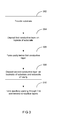
- FIG. 3 is a flowchart showing a first preferred fabrication method of making an aperture structure.
- FIGS. 4A-4E illustrate the steps of the flowchart in FIG. 3 .
- a silicon substrate is provided.
- FIG. 4A shows an initial silicon substrate 410.
- the silicon substrate is preferably a single crystal semiconductor silicon wafer.
- the silicon wafer is polished on both sides in order to facilitate smooth layer deposition and the eventual mounting of the die to an aperture support.
- the wafer thickness is not significant, so different wafer diameters may be used.
- a first conductive coating 420 ( FIG. 4B ) is deposited onto the top surface of the wafer 410.
- the first conductive coating is preferably metallic, and more preferably molybdenum.
- Other metals, such as tungsten, titanium, or platinum, and non-metals, such as graphite or conducting diamond (B-doped) can be used.
- Conductive coating 420 could be deposited by any known method, such as chemical vapor deposition (CVD), sputtering, or evaporation. A slightly tensile film is preferred to avoid buckling across the counter-bore or cavity opening.
- the substrate material is removed from a region of substrate 410 to form a cavity 430 below conductive layer 420 and expose the backside of a portion of conductive layer 420 as shown in FIG. 4C .
- the exposed portion of conductive layer 420 is referred to as the aperture opening defining portion 432.
- the aperture opening defining portion 432 may be the exposed portion of multiple conductive layers formed as a laminate.
- the substrate material can be etched, for example, using a deep reactive ion etch (DRIE) process.
- the cavity 430 is about 1.0 mm in diameter.
- the conductive layer 420 serves as an etch stop, thus the substrate etch proceeds to completion, ensuring that the bottom of the cavity 430 is entirely molybdenum.
- the lithographic patterning step used in the DRIE process is well known and not shown.
- a second conductive coating is deposited onto the backside of wafer and onto the exposed backside surface of layer 420, as well as on the sidewalls of cavity 430 as shown in FIG. 4D .
- the second conductive coating preferably comprises molybdenum, approximately 4 ⁇ m to 5 ⁇ m thick. Any deposition method could be used, such as the ones described above with respect to depositing conductive layer 420. Again, a slightly tensile film is preferred to avoid buckling of the aperture opening defining region across cavity 430.
- an aperture opening 450 is formed through the first and second conductive layers 420 and 440 as shown in FIG. 4E .
- Aperture opening 450 can be formed, for example, by photolithography or by ion beam milling.
- the combined thickness of the two conductive layers is preferably between 8 ⁇ m and 10 ⁇ m in this embodiment. Because the aperture opening is determined by the patterning of the conductive layer, instead of by the patterning of the substrate as in the prior art, the conductive layer can be much thicker, which produces a longer lasting aperture, resistant to ion beam etching.
- a substrate such as a silicon wafer
- FIG. 6A shows a silicon substrate, preferably a single crystal silicon wafer 610.
- the substrate is polished on both sides in order to facilitate layer deposition and eventual mounting of the die to an aperture rod or mounting device.
- the wafer thickness is not significant, so different wafer diameters may be used.
- a first conductive coating is deposited onto the top surface of the wafer 610, as shown in FIG. 6B .
- the first conductive coating can be deposited by the methods described above with respect to step 302 and can be composed of the same or similar materials as layer 420.
- the first conductive coating is preferably comprises a layer of molybdenum about 8 ⁇ m to 10 ⁇ m thick. Note that this deposition is thicker than the deposition of the conductive coating 420 of FIG. 4B because for this fabrication method, the final aperture opening defining region is comprised solely of the first molybdenum coating 620 material, not combined (or formed as a laminate of) first and second deposited conductive coatings 420 and 440 respectively of FIG. 4D and 4E . A slightly tensile film is preferred to avoid buckling across the cavity opening.
- a second conductive coating 630 ( FIG. 6C ) is applied to the bottom surface of the wafer 610, the side opposite of the first conductive coating 620.
- the materials of the second conductive layer can be, for example, those described with respect to the first conductive layer.
- both the first and second conductive layers comprise molybdenum, the second conductive layer approximately 4 ⁇ m to 5 ⁇ m thick. Any deposition method, such as the ones described above, can be used. A slightly tensile film is preferred to avoid buckling across the cavity opening.
- an opening 640 is etched into the second conductive coating 630 by lithographic patterning and subsequent first DRIE molybdenum etch.
- the resulting opening 640 is preferably about 1.0 mm in diameter in this embodiment and preferably serves as a hard mask for a second etch, such as a DRIE etch, in step 510.
- FIG. 6E shows the result of the etch process in step 510 forming a cavity 650 in the wafer 610 from the bottom side, using the conductive coating 630 on the bottom surface as a mask, forming cavity 650 into the wafer below conductive layer 620 and exposing the backside of a portion of conductive layer 620 as shown in FIG. 6E .
- the exposed portion of conductive layer 620 is referred to as the aperture opening defining portion 632.
- the aperture opening defining portion 632 may be the exposed portion of multiple conductive layers formed as a laminate.
- the cavity 650 size of the cavity is determined by the size of opening 640 and is preferably about 1.0 mm in diameter.
- the first molybdenum layer 620 serves as the etch stop, thus the silicon etch proceeds to completion, ensuring that the bottom of the cavity is entirely molybdenum.
- a third conductive layer 660 as shown in FIG. 6F is deposited from the back side of the wafer 610, coating the conductive layer 630, the walls of the etched cavity 650 in the substrate, and the bottom surface of conductive layer 620.
- a slightly tensile film is preferred to avoid buckling across the cavity opening.
- step 514 an anisotropic etch is applied to preferentially remove the third conductive layers from the back surface of the wafer 610 and from the bottom surface of conductive layer 620, while leaving a substantial portion of molybdenum remaining on the walls 670 of the cavity 650.
- the result of this step is that the conductive layer 620 from the first molybdenum deposition remains substantially intact, cantilevered across the cavity 650 as shown in FIG. 6G .
- the deposited thickness of layer 620 must be adequate to serve as an aperture.
- the substrate 610 be entirely encapsulated on all sides, including the side walls of cavity 650, by a protective layer of molybdenum or another metal since some processing steps may involve the use of XeF 2 , which will spontaneously attack and etch any exposed silicon surfaces.
- a hole is formed in layer 620 to form an aperture opening 680 as shown in FIG. 6H .
- the hole may be formed, for example, by photolithography or ion beam milling.
- the aperture opening 680 extends through the molybdenum layer 620 from the first molybdenum deposition, with a thickness between 8 and 10 ⁇ m.
- the size and shape of the aperture will vary with the requirements of the charged particle beam system.
- Apertures opening diameters typically vary from a few microns to hundreds of microns.
- the aperture opening is smaller than the diameter of the cavity, the charged particles are unaffected by the substrate.
- the diameter of the aperture opening is preferably less than 0.8 times the cavity diameter, more preferably less than 0.5 the cavity diameter, and most preferably less than 0.1 times the cavity diameter.
- the aperture opening shape is elliptical or oval.
- FIG. 7 shows an aperture strip 700 consisting of two rows with eight apertures 702 in each row.
- Aperture strip 700 includes sixteen cavities etched into the substrate 704.
- a through hole 706 located at the end of the aperture array enables the charged particle beam system operation effectively with no aperture blocking the beam - this hole also serves as a marker for the proper aperture strip orientation in the aperture motions assembly.
- An orientation marker 708 is etched into both sides of the aperture strip.
- aperture strips are selectively fabricated such that two or more aperture opening defining portion thicknesses are formed within the same aperture strip.
- the conductive coating thickness formed at the aperture opening can be different for one or more apertures within the same aperture strip thereby allowing a constant aspect ratio of apertures of different thicknesses to remain the same. As the diameter of the aperture opening gets larger, the thickness can also get larger to maintain a constant ratio of diameter to thickness.
- Some embodiments of the invention include an aperture structure for a charged particle beam system, the aperture structure comprising:
- the substrate comprises a semiconductor and the aperture material comprises a conductor.
- the substrate comprises silicon and the aperture material comprises molybdenum, tungsten, titanium, platinum, graphite or conducting diamond.
- the substrate is more than 10 times thicker than the aperture opening defining portion.
- the cavity in the substrate below the aperture opening defining portion has its shortest linear dimension normal to substrate surface at least ten times the longest linear dimension of the aperture opening normal to substrate surface.
- the closest distance from the material of the substrate material to the aperture opening is ten times the diameter of the aperture opening.
- At least two of the apertures are on a common substrate.
- Some embodiments of the invention include a charged particle beam column, comprising:
- Some embodiments of the invention include a method for fabricating a beam-defining aperture, comprising:
- Some embodiments further comprise depositing a second conductive layer on the bottom side of the substrate such that the wall of the cavity and bottom side of the first conductive layer are coated.
- depositing a first conductive layer comprises depositing tungsten, titanium, platinum, graphite or conducting diamond.
- depositing a first conductive layer comprises depositing a tensile structure.
- forming a cavity includes forming a cavity having a diameter of approximately 1 mm.
- Some embodiments of the invention include a method for fabricating a beam-defining aperture strip, comprising:
- the longest linear dimension of the aperture openings normal to the beam direction is less than 0.8 times the longest linear dimension of the aperture openings normal to the beam direction.
- the thickness of the first conductive layer is less than five times the thickness of the substrate.
- Some embodiments further comprise selectively depositing a third conductive coating forming a conductive laminate with the conductive coating at the aperture opening defining portion such that a one or more apertures have a conductive coating thickness at the aperture opening different from the remaining apertures within the same aperture strip.
Landscapes
- Physics & Mathematics (AREA)
- Chemical & Material Sciences (AREA)
- Analytical Chemistry (AREA)
- Spectroscopy & Molecular Physics (AREA)
- Engineering & Computer Science (AREA)
- General Engineering & Computer Science (AREA)
- High Energy & Nuclear Physics (AREA)
- Electron Beam Exposure (AREA)
Abstract
Description
- The present invention relates to charged particle beam systems, more specifically, beam-defining apertures in charged particle beam systems.
- In charged particle beam systems, such as electron microscopes or focused ion beam (FIB) systems, a source generates charged particles which are then focused by an optical column into a beam and directed onto the surface of a target to be imaged and/or processed. In the column, this beam may be blanked, that is, diverted into a stop to turn it off, deflected to move it around on the target surface.
- A beam having a lower beam current, that is, fewer charged particles, can typically be focused to a smaller diameter than a beam having a greater current. Using a lower beam current can therefore provide higher resolution imaging or processing. A lower beam current also results in less damage to the target.
- An ion beam can be used to mill or sputter material in controlled patterns from the surface of a target. The milling rate is roughly proportional to the beam current. Higher beam currents are therefore preferred when it is desired to quickly remove material, although the higher beam current typically results in lower resolution processing. Processing will sometimes use a two-step processing, with a high current beam to remove material quickly, and then a lower current beam to more precisely complete the milling
- Although an ideal beam would have all the ions uniformly distributed within a desired beam diameter, in actuality, the beam current distribution is more or less bell-shaped and tapers off away from the beam center. This "tail" reduces image resolution and makes it impossible to mill a straight vertical edge.
- Some applications require imaging, coarse milling, and fine milling. In particular, when a milled pattern needs to be precisely located with respect to a pre-existing feature on a target, it is necessary to first image the target with a lower current FIB, and then to switch to a higher current (typically larger diameter) FIB for coarse milling and then a lower current beam for fine milling. One important example of such an imaging/milling process is the preparation of thin "lamellae" (singular: "lamella") of various types of samples, such as semiconductor devices and cryo-frozen biological samples. In the case of semiconductor device failure analysis, a particular region of interest (Rol) within an integrated circuit, usually containing a defective device to be analyzed, is exposed by FIB milling on both sides, leaving a thin slice (lamella) of material remaining which contains the defective device - these lamellae are thin enough for use in high voltage transmission electron microscopes (TEMs) or scanning transmission electron microscopes (STEMs) where atomic resolutions are, in principle, available. Because the lamellae are only tens of nanometers thick, and the defects being observed may be on the scale of nanometers, the milling to create the lamella is extremely precise.
- During preparation of a lamella, it is necessary to switch between using large current, large diameter beams suitable for rapid milling, lower current, smaller diameter beam for fine milling, and even lower current, smaller diameter beams imaging. This is typically done by changing a beam-defining aperture (BDA) through which the beam passes. BDAs are typically holes in a metal strip, allowing only charged particles that pass through the hole to form the beam. There are typically several BDAs, or holes, in a metal strip, and switching apertures typically entails moving the strip so that a hole of a different diameter is positioned in the path of the beam.
-
FIG. 1 is a schematic cross-sectional view of aprior art aperture 100. Ahole 110 is formed in asilicon substrate 108 of roughly the size of the desired aperture hole. Layers may be deposited on the silicon substrate such as a SiO2 layer 106 and a SixNy layer 104 to aid in the formation of this hole. Amolybdenum layer 102 is then deposited on all surfaces conformally to protect the aperture from the ions in the ion beam. The layer is thin, typically 200-500 nm, to avoid substantially reducing the aperture hole diameter. Beam defining apertures in ion beam systems have a limited life because the ions in the ion beam impinge on the aperture structure, eroding it and expanding the hole. - An object of the invention is to provide an improved beam defining aperture for charged particle beam systems, including focused ion beam systems, transmission electron microscopes, scanning transmission electron microscopes, and scanning electron microscopes.
- The invention comprises new aperture structures and methods for fabricating these structures. A preferred aperture structure includes a deposited film supported by a substrate, where the aperture size and shape is not determined by (i.e., patterned into) the substrate.
- The foregoing has outlined rather broadly the features and technical advantages of the present invention in order that the detailed description of the invention that follows may be better understood. Additional features and advantages of the invention will be described hereinafter. It should be appreciated by those skilled in the art that the conception and specific embodiments disclosed may be readily utilized as a basis for modifying or designing other structures for carrying out the same purposes of the present invention. It should also be realized by those skilled in the art that such equivalent constructions do not depart from the spirit and scope of the invention as set forth in the appended claims.
- For a more thorough understanding of the present invention, and advantages thereof, reference is now made to the following descriptions taken in conjunction with the accompanying drawings, in which:
-
FIG. 1 is a schematic cross-sectional view of a prior art aperture. -
FIG. 2 is a micrograph of a prior art rectangular aperture showing some of the defects typically found in the sidewalls when fabricated using rolled molybdenum sheet metal. -
FIG. 3 is a flow chart showing a method of making an aperture. -
FIGS. 4A-4E illustrate the processing steps ofFIG. 3 . -
FIG. 5 is a flow chart showing another method of making an aperture. -
FIGS. 6A-6H illustrate the processing steps ofFIG. 5 . -
FIG. 7 shows an aperture strip fabricated in accordance with steps ofFIG. 3 orFIG. 5 . -
FIG. 8 shows an example layout of wafer on which are fabricated multiple apertures stripes similar to those shown inFIG. 7 . - Examination of prior art aperture holes has revealed many irregularities stemming from the methods used to form the aperture holes, including mechanical drilling, laser ablation, FIB-milling, etching, or electrical discharge machining (EDM). These irregularities include large burrs extending outwards from the aperture holes, irregularities in the aperture sidewalls, out-of-roundness and curtaining of the sidewalls (vertical grooves and ridges roughly parallel to the beam axis).
- Applicants have investigated the effect of aperture quality on the quality of the charged particle beams. Voids and patch fields observed on the sidewall structure of prior art molybdenum apertures are thought to cause undesirable deflections of charged particles passing through the apertures, especially of charged particles passing near the aperture sidewalls. This deflection causes the virtual source size to be enlarged, thereby making the focused beams at the substrate larger than they would be in the absence of these aperture wall effects.
-
FIG. 2 is a micrograph of a prior art molybdenum aperture 200 (rectangular opening 202 in this example), illustrating various undesirable aspects. This aperture was fabricated from a thin molybdenum sheet, which itself was formed by rolling of sintered molybdenum material. The sintered molybdenum has many microcrystallites and cavities - when rolled, these structures are flattened to form the layered material shown in the sidewall of the aperture.Delaminations 204 are visible, resulting in cavities within the material. The cavities are exposed during the process which creates the aperture hole, resulting in openings in the wall as shown. In addition, "patch fields" 206 with differing work functions are also revealed during the aperture-forming process - these patch fields appear dark or bright in secondary electron imaging as shown. Both the patch fields and cavities may have deleterious effects on charged particle beams passing through the aperture due to induced local perturbations of the electric field within and near the aperture. - Moreover, some prior art methods used to manufacture the aperture structures are expensive. If an aperture strip has a large range of hole diameters, it is typically necessary to form counter-bores or cavities at the locations of the smaller holes to maintain aperture aspect ratios (i.e., the ratios of the length of the hole to the hole diameter) within a range of typically 0.5 to 2.0 - forming these counter-bores or cavities further increases the cost of the aperture strip. The holes are typically individually formed (by drilling, laser ablation, FIB-milling, etching, or EDM) and the fabrication process is serial (i.e., one aperture hole is formed at a time).
- In the typical prior art fabrication sequence, the aperture hole diameter is determined by the
hole 110 etched in the silicon substrate prior to deposition of the molybdenum, not in the deposited molybdenum layer during or after deposition. A disadvantage of this fabrication method is that the molybdenum is necessarily relatively thin to avoid decreasing the final aperture opening size. In a FIB system, where the beam will sputter the aperture material, the thin molybdenum layer will rapidly deteriorate, resulting in short aperture lifetimes. - A preferred embodiment of the invention includes a substrate of a first material and an aperture material different from the substrate material. The portion of the aperture material around the hole is not directly supported by the substrate, that is, the aperture material is cantilevered over a hole in the substrate, like a drum skin over a drum frame. That is, there is a cavity or hole in the substrate under an opening portion of the aperture material. The aperture opening is therefore defined by a hole in the aperture material, not by a hole in the substrate. The patterning of the aperture material therefore determining the aperture opening, not the patterning of the substrate.
-
FIG. 3 is a flowchart showing a first preferred fabrication method of making an aperture structure.FIGS. 4A-4E illustrate the steps of the flowchart inFIG. 3 . - In
step 302, a silicon substrate is provided.FIG. 4A shows aninitial silicon substrate 410. The silicon substrate is preferably a single crystal semiconductor silicon wafer. Preferably, the silicon wafer is polished on both sides in order to facilitate smooth layer deposition and the eventual mounting of the die to an aperture support. The wafer thickness is not significant, so different wafer diameters may be used. - In
step 304, a first conductive coating 420 (FIG. 4B ) is deposited onto the top surface of thewafer 410. The first conductive coating is preferably metallic, and more preferably molybdenum. Other metals, such as tungsten, titanium, or platinum, and non-metals, such as graphite or conducting diamond (B-doped) can be used.Conductive coating 420 could be deposited by any known method, such as chemical vapor deposition (CVD), sputtering, or evaporation. A slightly tensile film is preferred to avoid buckling across the counter-bore or cavity opening. - In
step 306, the substrate material is removed from a region ofsubstrate 410 to form acavity 430 belowconductive layer 420 and expose the backside of a portion ofconductive layer 420 as shown inFIG. 4C . The exposed portion ofconductive layer 420 is referred to as the apertureopening defining portion 432. The apertureopening defining portion 432 may be the exposed portion of multiple conductive layers formed as a laminate. The substrate material can be etched, for example, using a deep reactive ion etch (DRIE) process. In some embodiments, thecavity 430 is about 1.0 mm in diameter. For this etch step, theconductive layer 420 serves as an etch stop, thus the substrate etch proceeds to completion, ensuring that the bottom of thecavity 430 is entirely molybdenum. The lithographic patterning step used in the DRIE process is well known and not shown. - In
step 308, a second conductive coating is deposited onto the backside of wafer and onto the exposed backside surface oflayer 420, as well as on the sidewalls ofcavity 430 as shown inFIG. 4D . The second conductive coating preferably comprises molybdenum, approximately 4 µm to 5 µm thick. Any deposition method could be used, such as the ones described above with respect to depositingconductive layer 420. Again, a slightly tensile film is preferred to avoid buckling of the aperture opening defining region acrosscavity 430. - In
step 310, anaperture opening 450 is formed through the first and secondconductive layers FIG. 4E .Aperture opening 450 can be formed, for example, by photolithography or by ion beam milling. The combined thickness of the two conductive layers is preferably between 8 µm and 10 µm in this embodiment. Because the aperture opening is determined by the patterning of the conductive layer, instead of by the patterning of the substrate as in the prior art, the conductive layer can be much thicker, which produces a longer lasting aperture, resistant to ion beam etching. -
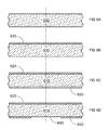
FIG. 5 is a flowchart showing a second preferred fabrication method of making an aperture structure.FIGS. 6A-6H illustrates the steps of the flowchart inFIG. 5 . - In
step 502, a substrate, such as a silicon wafer, is provided.FIG. 6A shows a silicon substrate, preferably a singlecrystal silicon wafer 610. Preferably, the substrate is polished on both sides in order to facilitate layer deposition and eventual mounting of the die to an aperture rod or mounting device. The wafer thickness is not significant, so different wafer diameters may be used. - In
step 504, a first conductive coating is deposited onto the top surface of thewafer 610, as shown inFIG. 6B . The first conductive coating can be deposited by the methods described above with respect to step 302 and can be composed of the same or similar materials aslayer 420. The first conductive coating is preferably comprises a layer of molybdenum about 8 µm to 10 µm thick. Note that this deposition is thicker than the deposition of theconductive coating 420 ofFIG. 4B because for this fabrication method, the final aperture opening defining region is comprised solely of thefirst molybdenum coating 620 material, not combined (or formed as a laminate of) first and second depositedconductive coatings FIG. 4D and 4E . A slightly tensile film is preferred to avoid buckling across the cavity opening. - In
optional step 506, a second conductive coating 630 (FIG. 6C ) is applied to the bottom surface of thewafer 610, the side opposite of the firstconductive coating 620. The materials of the second conductive layer can be, for example, those described with respect to the first conductive layer. In one embodiment, both the first and second conductive layers comprise molybdenum, the second conductive layer approximately 4 µm to 5 µm thick. Any deposition method, such as the ones described above, can be used. A slightly tensile film is preferred to avoid buckling across the cavity opening. - In
step 508, anopening 640 is etched into the secondconductive coating 630 by lithographic patterning and subsequent first DRIE molybdenum etch. The resultingopening 640 is preferably about 1.0 mm in diameter in this embodiment and preferably serves as a hard mask for a second etch, such as a DRIE etch, instep 510. -
FIG. 6E shows the result of the etch process instep 510 forming acavity 650 in thewafer 610 from the bottom side, using theconductive coating 630 on the bottom surface as a mask, formingcavity 650 into the wafer belowconductive layer 620 and exposing the backside of a portion ofconductive layer 620 as shown inFIG. 6E . The exposed portion ofconductive layer 620 is referred to as the apertureopening defining portion 632. The apertureopening defining portion 632 may be the exposed portion of multiple conductive layers formed as a laminate. Thecavity 650 size of the cavity is determined by the size ofopening 640 and is preferably about 1.0 mm in diameter. Thefirst molybdenum layer 620 serves as the etch stop, thus the silicon etch proceeds to completion, ensuring that the bottom of the cavity is entirely molybdenum. - In
step 512, a thirdconductive layer 660 as shown inFIG. 6F , preferably molybdenum, is deposited from the back side of thewafer 610, coating theconductive layer 630, the walls of the etchedcavity 650 in the substrate, and the bottom surface ofconductive layer 620. A slightly tensile film is preferred to avoid buckling across the cavity opening. - In
step 514, an anisotropic etch is applied to preferentially remove the third conductive layers from the back surface of thewafer 610 and from the bottom surface ofconductive layer 620, while leaving a substantial portion of molybdenum remaining on thewalls 670 of thecavity 650. The result of this step is that theconductive layer 620 from the first molybdenum deposition remains substantially intact, cantilevered across thecavity 650 as shown inFIG. 6G . Thus the deposited thickness oflayer 620 must be adequate to serve as an aperture. It is preferred, although not required in all embodiments, that thesubstrate 610 be entirely encapsulated on all sides, including the side walls ofcavity 650, by a protective layer of molybdenum or another metal since some processing steps may involve the use of XeF2, which will spontaneously attack and etch any exposed silicon surfaces. - In
step 516, a hole is formed inlayer 620 to form anaperture opening 680 as shown inFIG. 6H . The hole may be formed, for example, by photolithography or ion beam milling. Theaperture opening 680 extends through themolybdenum layer 620 from the first molybdenum deposition, with a thickness between 8 and 10 µm. - The size and shape of the aperture will vary with the requirements of the charged particle beam system. Apertures opening diameters typically vary from a few microns to hundreds of microns. The aperture opening is smaller than the diameter of the cavity, the charged particles are unaffected by the substrate. The diameter of the aperture opening is preferably less than 0.8 times the cavity diameter, more preferably less than 0.5 the cavity diameter, and most preferably less than 0.1 times the cavity diameter. In some embodiments, the aperture opening shape is elliptical or oval. When the aperture opening is not circular, the longest linear diameter of the aperture opening, normal to the substrate surface, is preferably less than 0.8 times the shortest linear dimension of the cavity normal to the substrate surface, more preferably less than 0.5 the shortest linear dimension of the cavity normal to the substrate surface, and most preferably less than 0.1 times the shortest linear dimension of the cavity normal to the substrate surface. The term "diameter" is used to refer to any major linear dimension of the opening, normal to the beam axis. The substrate is typically more than five times thicker than the aperture opening portion, more than 10 times thicker than the aperture opening portion, or more than 20 timers thicker than the aperture opening portion. In some embodiments, the aperture opening shape is a rectangular slit. Example widths of the aperture slit can be in the range from 1.0-3.0 µm with lengths around 500 µm.
-
FIG. 7 shows anaperture strip 700 consisting of two rows with eightapertures 702 in each row.Aperture strip 700 includes sixteen cavities etched into thesubstrate 704. A throughhole 706 located at the end of the aperture array enables the charged particle beam system operation effectively with no aperture blocking the beam - this hole also serves as a marker for the proper aperture strip orientation in the aperture motions assembly. Anorientation marker 708 is etched into both sides of the aperture strip. - In another embodiment, aperture strips are selectively fabricated such that two or more aperture opening defining portion thicknesses are formed within the same aperture strip. In other words, the conductive coating thickness formed at the aperture opening can be different for one or more apertures within the same aperture strip thereby allowing a constant aspect ratio of apertures of different thicknesses to remain the same. As the diameter of the aperture opening gets larger, the thickness can also get larger to maintain a constant ratio of diameter to thickness.
-
FIG. 8 shows an example layout 800 of one hundred ten aperture dice 802 (seeFIG. 7 ) arranged on a 150 mm diameter wafer. The kerf or scribe alley widths are not shown, but there is adequate edge exclusion to account for any necessary kerf widths without needing to change the layout. Any size wafer can be used in the fabrication process of the aperture strip. - Some embodiments of the invention include an aperture structure for a charged particle beam system, the aperture structure comprising:
- a substrate;
- an aperture material supported by the substrate and having an aperture opening defining portion including a hole defining an aperture opening; and
- a cavity in the substrate material below the aperture opening defining portion, so that the aperture is defined by the hole in the aperture material and not by the cavity in the substrate.
- In some embodiments, the substrate comprises a semiconductor and the aperture material comprises a conductor.
- In some embodiments, the substrate comprises silicon and the aperture material comprises molybdenum, tungsten, titanium, platinum, graphite or conducting diamond.
- In some embodiments, the substrate is more than 10 times thicker than the aperture opening defining portion.
- In some embodiments, the cavity in the substrate below the aperture opening defining portion has its shortest linear dimension normal to substrate surface at least ten times the longest linear dimension of the aperture opening normal to substrate surface.
- In some embodiments, the closest distance from the material of the substrate material to the aperture opening is ten times the diameter of the aperture opening.
- In some embodiments, at least two of the apertures are on a common substrate.
- Some embodiments of the invention include a charged particle beam column, comprising:
- a source of charged particles; and
- a focusing column for focusing the charged particles, the focusing column including an aperture strip as described above.
- Some embodiments of the invention include a method for fabricating a beam-defining aperture, comprising:
- depositing a first conductive layer on the top side of a substrate;
- forming a cavity on the bottom side of the substrate which exposes a portion of the bottom side of the first conductive layer; and
- forming a hole in the conductive layer, the hole opening into the cavity so that the aperture defined by the hole is determined by the patterning on the conductive coating and not by the cavity size.
- Some embodiments further comprise depositing a second conductive layer on the bottom side of the substrate such that the wall of the cavity and bottom side of the first conductive layer are coated.
- In some embodiments, depositing a first conductive layer comprises depositing molybdenum.
- In some embodiments, depositing a first conductive layer comprises depositing tungsten, titanium, platinum, graphite or conducting diamond.
- In some embodiments, depositing a first conductive layer comprises depositing a tensile structure.
- In some embodiments, forming a cavity includes forming a cavity having a diameter of approximately 1 mm.
- In some embodiments, forming a hole in the conductive layer includes forming a hole in the form of a circle, oval, or rectangular slit.
- Some embodiments of the invention include a method for fabricating a beam-defining aperture strip, comprising:
- depositing a first conductive coating on the top side of a substrate;
- forming a plurality of cavities on the bottom side of the substrate, the cavities exposing the bottom side of the first conductive coating;
- forming aperture openings through the first conductive layer, above one or more of the cavities; and
- dividing the substrate into multiple aperture strips.
- In some embodiments, the longest linear dimension of the aperture openings normal to the beam direction is less than 0.8 times the longest linear dimension of the aperture openings normal to the beam direction.
- In some embodiments, the thickness of the first conductive layer is less than five times the thickness of the substrate.
- Some embodiments further comprise selectively depositing a third conductive coating forming a conductive laminate with the conductive coating at the aperture opening defining portion such that a one or more apertures have a conductive coating thickness at the aperture opening different from the remaining apertures within the same aperture strip.
- Although the present invention and its advantages have been described in detail, it should be understood that various changes, substitutions and alterations can be made herein without departing from the spirit and scope of the invention as defined by the appended claims. For example, while the embodiments describe one aperture opening per substrate cavity, some embodiments could have multiple aperture openings per cavity. For example, a long, thin cavity could include multiple aperture openings. Coating the sides of the cavity with a conductor may be unnecessary in some embodiments.
- Moreover, the scope of the present application is not intended to be limited to the particular embodiments of the process, machine, manufacture, composition of matter, means, methods and steps described in the specification. As one of ordinary skill in the art will readily appreciate from the disclosure of the present invention, processes, machines, manufacture, compositions of matter, means, methods, or steps, presently existing or later to be developed that perform substantially the same function or achieve substantially the same result as the corresponding embodiments described herein may be utilized according to the present invention. Accordingly, the appended claims are intended to include within their scope such processes, machines, manufacture, compositions of matter, means, methods, or steps.
Claims (15)
- An aperture structure for a charged particle beam system, the aperture structure comprising:a substrate (410, 610);an aperture material (420, 620) supported by the substrate and having an aperture opening defining portion (432, 632) including a hole ( 450, 680) defining an aperture opening; anda cavity (430, 650) in the substrate material below the aperture opening defining portion;characterized in that the aperture is defined by the hole in the aperture material and not by the cavity in the substrate.
- The aperture structure of claim 1 in which:the substrate comprises a substrate material; andthe closest distance from the substrate material to the aperture opening is ten times the diameter of the aperture opening.
- The aperture structure of claim 1 in which the substrate comprises a semiconductor and the aperture material comprises a conductor.
- The aperture structure of claim 3 in which the substrate comprises silicon and the aperture material comprises molybdenum, tungsten, titanium, platinum, graphite or conducting diamond.
- The aperture structure of any of the above claims in which the substrate is more than 10 times thicker than the aperture opening defining portion.
- The aperture structure of any of the above claims in which the cavity in the substrate below the aperture opening defining portion has its shortest linear dimension normal to substrate surface at least ten times the longest linear dimension of the aperture opening normal to substrate surface.
- An aperture strip comprising at least two of the apertures of any of the above claims on a common substrate.
- A charged particle beam column, comprising:a source of charged particles;a focusing column for focusing the charged particles;characterized in that the focusing column includes the aperture strip of claim 7.
- A method for fabricating a beam-defining aperture, comprising:depositing a first conductive layer (420, 620) on the top side of a substrate;forming a cavity on the bottom side of the substrate which exposes a portion of the bottom side of the first conductive layer; andforming a hole in the conductive layer (450, 680), the hole opening into the cavity so that the aperture defined by the hole is determined by the patterning on the conductive coating and not by the cavity size.
- The method of claim 9 further comprising depositing a second conductive layer (440, 630) on the bottom side of the substrate such that the wall of the cavity and bottom side of the first conductive layer are coated.
- The method of claim 9 or claim 10 in which depositing the first conductive layer comprises depositing molybdenum, tungsten, titanium, platinum, graphite or conducting diamond.
- The method of any of claims 9-11 in which depositing the first conductive layer comprises depositing a tensile structure.
- The method of any of claims 9-12 in which forming the cavity includes forming the cavity having a diameter of approximately 1 mm.
- The method of any of claims 9-13 in which forming the hole in the conductive layer includes forming the hole in the form of a circle, oval, or rectangular slit.
- The method of any of claims 9-13 in which:forming a cavity on the bottom side of the substrate includes forming multiple cavities on the bottom side of the substrate, the cavities exposing the bottom side of the first conductive coating;forming a hole in the conductive layer includes forming a hole in the first conductive layer above each of the multiple cavities, the holes opening into the cavities so that apertures defined by the holes are determined by the patterning on the conductive coating and not by the cavity size; anddividing the substrate into multiple aperture strips.
Applications Claiming Priority (1)
| Application Number | Priority Date | Filing Date | Title |
|---|---|---|---|
| US201161556690P | 2011-11-07 | 2011-11-07 |
Publications (3)
| Publication Number | Publication Date |
|---|---|
| EP2590203A2 true EP2590203A2 (en) | 2013-05-08 |
| EP2590203A3 EP2590203A3 (en) | 2014-06-04 |
| EP2590203B1 EP2590203B1 (en) | 2017-02-01 |
Family
ID=47115607
Family Applications (1)
| Application Number | Title | Priority Date | Filing Date |
|---|---|---|---|
| EP12191348.7A Active EP2590203B1 (en) | 2011-11-07 | 2012-11-06 | Method of fabricating a beam-defining aperture for a focused ion beam and beam definition of a focused ion beam with such an aperture |
Country Status (4)
| Country | Link |
|---|---|
| US (1) | US8907296B2 (en) |
| EP (1) | EP2590203B1 (en) |
| JP (1) | JP2013101929A (en) |
| CN (1) | CN103094031B (en) |
Cited By (3)
| Publication number | Priority date | Publication date | Assignee | Title |
|---|---|---|---|---|
| US8759764B2 (en) | 2012-06-29 | 2014-06-24 | Fei Company | On-axis detector for charged particle beam system |
| US8907296B2 (en) | 2011-11-07 | 2014-12-09 | Fei Company | Charged particle beam system aperture |
| US9733164B2 (en) | 2012-06-11 | 2017-08-15 | Fei Company | Lamella creation method and device using fixed-angle beam and rotating sample stage |
Families Citing this family (4)
| Publication number | Priority date | Publication date | Assignee | Title |
|---|---|---|---|---|
| EP3010031B1 (en) * | 2014-10-16 | 2017-03-22 | Fei Company | Charged Particle Microscope with special aperture plate |
| CN104599927B (en) * | 2014-12-24 | 2016-11-30 | 西安理工大学 | A kind of preparation method of porous diaphragm |
| US9679742B2 (en) | 2015-10-30 | 2017-06-13 | Fei Company | Method for optimizing charged particle beams formed by shaped apertures |
| CN113228220A (en) * | 2018-12-26 | 2021-08-06 | Asml荷兰有限公司 | Method for manufacturing aperture device |
Family Cites Families (18)
| Publication number | Priority date | Publication date | Assignee | Title |
|---|---|---|---|---|
| DE2425464C3 (en) * | 1974-05-27 | 1978-11-02 | Siemens Ag, 1000 Berlin Und 8000 Muenchen | Process for the production of thin-film aperture diaphragms for particle beam devices |
| JPS6081751A (en) * | 1983-10-11 | 1985-05-09 | Nec Corp | Aperture drawing and its manufacturing method |
| US5899728A (en) * | 1997-12-22 | 1999-05-04 | Motorola, Inc. | Method of forming a lithographic mask |
| EP1388883B1 (en) | 2002-08-07 | 2013-06-05 | Fei Company | Coaxial FIB-SEM column |
| US7009187B2 (en) | 2002-08-08 | 2006-03-07 | Fei Company | Particle detector suitable for detecting ions and electrons |
| US7504182B2 (en) | 2002-09-18 | 2009-03-17 | Fei Company | Photolithography mask repair |
| RU2249241C1 (en) * | 2003-11-04 | 2005-03-27 | Гурович Борис Аронович | Image creator |
| EP2287883B1 (en) * | 2004-04-15 | 2017-08-16 | Carl Zeiss SMT GmbH | Apparatus and method for investigating or modifying a surface with a beam of charged particles |
| JP4528589B2 (en) * | 2004-09-27 | 2010-08-18 | 株式会社アドバンテスト | Mask inspection apparatus, mask inspection method, and electron beam exposure apparatus |
| EP2041756B1 (en) | 2006-07-14 | 2015-05-13 | FEI Company | A multi-source plasma focused ion beam system |
| JP2008204675A (en) | 2007-02-19 | 2008-09-04 | Hitachi High-Technologies Corp | Electron microscope, diaphragm plate used therefor, and method for producing diaphragm plate |
| WO2009089499A2 (en) | 2008-01-09 | 2009-07-16 | Fei Company | Multibeam system |
| EP2313230A4 (en) | 2008-07-09 | 2017-03-08 | FEI Company | Method and apparatus for laser machining |
| US8278220B2 (en) | 2008-08-08 | 2012-10-02 | Fei Company | Method to direct pattern metals on a substrate |
| US8168961B2 (en) | 2008-11-26 | 2012-05-01 | Fei Company | Charged particle beam masking for laser ablation micromachining |
| JP5756585B2 (en) | 2010-04-07 | 2015-07-29 | エフ・イ−・アイ・カンパニー | Combined laser and charged particle beam system |
| US8283629B1 (en) | 2011-04-15 | 2012-10-09 | Fei Company | Aberration-corrected wien ExB mass filter with removal of neutrals from the Beam |
| JP2013101929A (en) | 2011-11-07 | 2013-05-23 | Fei Co | Charged particle beam system aperture |
-
2012
- 2012-11-02 JP JP2012242805A patent/JP2013101929A/en active Pending
- 2012-11-06 US US13/669,626 patent/US8907296B2/en active Active
- 2012-11-06 EP EP12191348.7A patent/EP2590203B1/en active Active
- 2012-11-06 CN CN201210438995.0A patent/CN103094031B/en active Active
Non-Patent Citations (1)
| Title |
|---|
| None |
Cited By (3)
| Publication number | Priority date | Publication date | Assignee | Title |
|---|---|---|---|---|
| US8907296B2 (en) | 2011-11-07 | 2014-12-09 | Fei Company | Charged particle beam system aperture |
| US9733164B2 (en) | 2012-06-11 | 2017-08-15 | Fei Company | Lamella creation method and device using fixed-angle beam and rotating sample stage |
| US8759764B2 (en) | 2012-06-29 | 2014-06-24 | Fei Company | On-axis detector for charged particle beam system |
Also Published As
| Publication number | Publication date |
|---|---|
| US8907296B2 (en) | 2014-12-09 |
| CN103094031B (en) | 2017-05-24 |
| EP2590203A3 (en) | 2014-06-04 |
| EP2590203B1 (en) | 2017-02-01 |
| CN103094031A (en) | 2013-05-08 |
| JP2013101929A (en) | 2013-05-23 |
| US20130181140A1 (en) | 2013-07-18 |
Similar Documents
| Publication | Publication Date | Title |
|---|---|---|
| US8907296B2 (en) | Charged particle beam system aperture | |
| US9653309B2 (en) | Method for fabrication of high aspect ratio trenches and formation of nanoscale features therefrom | |
| US9336985B2 (en) | Method for creating S/TEM sample and sample structure | |
| US8884247B2 (en) | System and method for ex situ analysis of a substrate | |
| CN100580865C (en) | Device and method for investigating or modifying a surface with a charged particle beam | |
| US20130306878A1 (en) | Electrode of electrostatic lens and method of manufacturing the same | |
| KR20030024552A (en) | A semiconductor device and a manufacturing method of the same | |
| KR20010051732A (en) | Method of electron-beam exposure and mask and electron-beam exposure system used therein | |
| JP2009198412A (en) | Preparation method of sample for transmission electron microscope, and sample for transmission electron microscope | |
| US20110027998A1 (en) | Method of Manufacturing A Nano Structure By Etching, Using A Substrate Containing Silicon | |
| EP3234695B1 (en) | Mirror device | |
| US10401265B1 (en) | Methods for acquiring planar view stem images of device structures | |
| JP2011243540A (en) | Selected area aperture plate of transmission electron microscope, manufacturing method of selected area aperture plate, and observing method of selected area electron diffraction image | |
| WO2025113824A1 (en) | Method for producing a micro-optical unit for a multiple particle beam system, micro-optical unit and multiple particle beam system | |
| TW202603771A (en) | Image generation with improved scaning lines for smart charge distribution | |
| Atiqah et al. | Application of focused ion beam micromachining: a review | |
| US6251782B1 (en) | Specimen preparation by focused ion beam technique | |
| KR20180027346A (en) | Conductive contact neddle and charged particle beam apparatus | |
| JPH09186138A (en) | Ion beam processing apparatus | |
| KR20050033699A (en) | Method for forming sample using analysis by tem | |
| JP2014033077A (en) | Through-hole formation method | |
| KR20070016023A (en) | Grid structure for fixing sample of electron microscope | |
| DE102024105793B3 (en) | Manufacturing process for a monolithic multi-aperture plate and monolithic multi-aperture plate for a multi-beam electron beam system | |
| US8614427B1 (en) | Suspended membrane calibration sample | |
| CN119804090B (en) | Method of processing transmission samples using focused ion beam |
Legal Events
| Date | Code | Title | Description |
|---|---|---|---|
| PUAI | Public reference made under article 153(3) epc to a published international application that has entered the european phase |
Free format text: ORIGINAL CODE: 0009012 |
|
| AK | Designated contracting states |
Kind code of ref document: A2 Designated state(s): AL AT BE BG CH CY CZ DE DK EE ES FI FR GB GR HR HU IE IS IT LI LT LU LV MC MK MT NL NO PL PT RO RS SE SI SK SM TR |
|
| AX | Request for extension of the european patent |
Extension state: BA ME |
|
| PUAL | Search report despatched |
Free format text: ORIGINAL CODE: 0009013 |
|
| AK | Designated contracting states |
Kind code of ref document: A3 Designated state(s): AL AT BE BG CH CY CZ DE DK EE ES FI FR GB GR HR HU IE IS IT LI LT LU LV MC MK MT NL NO PL PT RO RS SE SI SK SM TR |
|
| AX | Request for extension of the european patent |
Extension state: BA ME |
|
| RIC1 | Information provided on ipc code assigned before grant |
Ipc: H01J 37/09 20060101AFI20140430BHEP |
|
| RBV | Designated contracting states (corrected) |
Designated state(s): AL AT BE BG CH CY CZ DE DK EE ES FI FR GB GR HR HU IE IS IT LI LT LU LV MC MK MT NL NO PL PT RO RS SE SI SK SM TR |
|
| 17P | Request for examination filed |
Effective date: 20141205 |
|
| 17Q | First examination report despatched |
Effective date: 20160120 |
|
| GRAP | Despatch of communication of intention to grant a patent |
Free format text: ORIGINAL CODE: EPIDOSNIGR1 |
|
| GRAJ | Information related to disapproval of communication of intention to grant by the applicant or resumption of examination proceedings by the epo deleted |
Free format text: ORIGINAL CODE: EPIDOSDIGR1 |
|
| INTG | Intention to grant announced |
Effective date: 20160926 |
|
| INTC | Intention to grant announced (deleted) | ||
| GRAP | Despatch of communication of intention to grant a patent |
Free format text: ORIGINAL CODE: EPIDOSNIGR1 |
|
| INTG | Intention to grant announced |
Effective date: 20161108 |
|
| GRAS | Grant fee paid |
Free format text: ORIGINAL CODE: EPIDOSNIGR3 |
|
| GRAA | (expected) grant |
Free format text: ORIGINAL CODE: 0009210 |
|
| AK | Designated contracting states |
Kind code of ref document: B1 Designated state(s): AL AT BE BG CH CY CZ DE DK EE ES FI FR GB GR HR HU IE IS IT LI LT LU LV MC MK MT NL NO PL PT RO RS SE SI SK SM TR |
|
| REG | Reference to a national code |
Ref country code: GB Ref legal event code: FG4D |
|
| REG | Reference to a national code |
Ref country code: CH Ref legal event code: EP Ref country code: AT Ref legal event code: REF Ref document number: 866188 Country of ref document: AT Kind code of ref document: T Effective date: 20170215 |
|
| REG | Reference to a national code |
Ref country code: IE Ref legal event code: FG4D |
|
| REG | Reference to a national code |
Ref country code: DE Ref legal event code: R096 Ref document number: 602012028204 Country of ref document: DE |
|
| REG | Reference to a national code |
Ref country code: NL Ref legal event code: MP Effective date: 20170201 |
|
| REG | Reference to a national code |
Ref country code: LT Ref legal event code: MG4D |
|
| REG | Reference to a national code |
Ref country code: AT Ref legal event code: MK05 Ref document number: 866188 Country of ref document: AT Kind code of ref document: T Effective date: 20170201 |
|
| PG25 | Lapsed in a contracting state [announced via postgrant information from national office to epo] |
Ref country code: FI Free format text: LAPSE BECAUSE OF FAILURE TO SUBMIT A TRANSLATION OF THE DESCRIPTION OR TO PAY THE FEE WITHIN THE PRESCRIBED TIME-LIMIT Effective date: 20170201 Ref country code: IS Free format text: LAPSE BECAUSE OF FAILURE TO SUBMIT A TRANSLATION OF THE DESCRIPTION OR TO PAY THE FEE WITHIN THE PRESCRIBED TIME-LIMIT Effective date: 20170601 Ref country code: LT Free format text: LAPSE BECAUSE OF FAILURE TO SUBMIT A TRANSLATION OF THE DESCRIPTION OR TO PAY THE FEE WITHIN THE PRESCRIBED TIME-LIMIT Effective date: 20170201 Ref country code: NO Free format text: LAPSE BECAUSE OF FAILURE TO SUBMIT A TRANSLATION OF THE DESCRIPTION OR TO PAY THE FEE WITHIN THE PRESCRIBED TIME-LIMIT Effective date: 20170501 Ref country code: HR Free format text: LAPSE BECAUSE OF FAILURE TO SUBMIT A TRANSLATION OF THE DESCRIPTION OR TO PAY THE FEE WITHIN THE PRESCRIBED TIME-LIMIT Effective date: 20170201 Ref country code: GR Free format text: LAPSE BECAUSE OF FAILURE TO SUBMIT A TRANSLATION OF THE DESCRIPTION OR TO PAY THE FEE WITHIN THE PRESCRIBED TIME-LIMIT Effective date: 20170502 |
|
| PG25 | Lapsed in a contracting state [announced via postgrant information from national office to epo] |
Ref country code: RS Free format text: LAPSE BECAUSE OF FAILURE TO SUBMIT A TRANSLATION OF THE DESCRIPTION OR TO PAY THE FEE WITHIN THE PRESCRIBED TIME-LIMIT Effective date: 20170201 Ref country code: BG Free format text: LAPSE BECAUSE OF FAILURE TO SUBMIT A TRANSLATION OF THE DESCRIPTION OR TO PAY THE FEE WITHIN THE PRESCRIBED TIME-LIMIT Effective date: 20170501 Ref country code: ES Free format text: LAPSE BECAUSE OF FAILURE TO SUBMIT A TRANSLATION OF THE DESCRIPTION OR TO PAY THE FEE WITHIN THE PRESCRIBED TIME-LIMIT Effective date: 20170201 Ref country code: PL Free format text: LAPSE BECAUSE OF FAILURE TO SUBMIT A TRANSLATION OF THE DESCRIPTION OR TO PAY THE FEE WITHIN THE PRESCRIBED TIME-LIMIT Effective date: 20170201 Ref country code: LV Free format text: LAPSE BECAUSE OF FAILURE TO SUBMIT A TRANSLATION OF THE DESCRIPTION OR TO PAY THE FEE WITHIN THE PRESCRIBED TIME-LIMIT Effective date: 20170201 Ref country code: AT Free format text: LAPSE BECAUSE OF FAILURE TO SUBMIT A TRANSLATION OF THE DESCRIPTION OR TO PAY THE FEE WITHIN THE PRESCRIBED TIME-LIMIT Effective date: 20170201 Ref country code: PT Free format text: LAPSE BECAUSE OF FAILURE TO SUBMIT A TRANSLATION OF THE DESCRIPTION OR TO PAY THE FEE WITHIN THE PRESCRIBED TIME-LIMIT Effective date: 20170601 Ref country code: NL Free format text: LAPSE BECAUSE OF FAILURE TO SUBMIT A TRANSLATION OF THE DESCRIPTION OR TO PAY THE FEE WITHIN THE PRESCRIBED TIME-LIMIT Effective date: 20170201 Ref country code: SE Free format text: LAPSE BECAUSE OF FAILURE TO SUBMIT A TRANSLATION OF THE DESCRIPTION OR TO PAY THE FEE WITHIN THE PRESCRIBED TIME-LIMIT Effective date: 20170201 |
|
| REG | Reference to a national code |
Ref country code: FR Ref legal event code: PLFP Year of fee payment: 6 |
|
| PG25 | Lapsed in a contracting state [announced via postgrant information from national office to epo] |
Ref country code: CZ Free format text: LAPSE BECAUSE OF FAILURE TO SUBMIT A TRANSLATION OF THE DESCRIPTION OR TO PAY THE FEE WITHIN THE PRESCRIBED TIME-LIMIT Effective date: 20170201 Ref country code: RO Free format text: LAPSE BECAUSE OF FAILURE TO SUBMIT A TRANSLATION OF THE DESCRIPTION OR TO PAY THE FEE WITHIN THE PRESCRIBED TIME-LIMIT Effective date: 20170201 Ref country code: IT Free format text: LAPSE BECAUSE OF FAILURE TO SUBMIT A TRANSLATION OF THE DESCRIPTION OR TO PAY THE FEE WITHIN THE PRESCRIBED TIME-LIMIT Effective date: 20170201 Ref country code: SK Free format text: LAPSE BECAUSE OF FAILURE TO SUBMIT A TRANSLATION OF THE DESCRIPTION OR TO PAY THE FEE WITHIN THE PRESCRIBED TIME-LIMIT Effective date: 20170201 Ref country code: EE Free format text: LAPSE BECAUSE OF FAILURE TO SUBMIT A TRANSLATION OF THE DESCRIPTION OR TO PAY THE FEE WITHIN THE PRESCRIBED TIME-LIMIT Effective date: 20170201 |
|
| REG | Reference to a national code |
Ref country code: DE Ref legal event code: R097 Ref document number: 602012028204 Country of ref document: DE |
|
| PG25 | Lapsed in a contracting state [announced via postgrant information from national office to epo] |
Ref country code: DK Free format text: LAPSE BECAUSE OF FAILURE TO SUBMIT A TRANSLATION OF THE DESCRIPTION OR TO PAY THE FEE WITHIN THE PRESCRIBED TIME-LIMIT Effective date: 20170201 Ref country code: SM Free format text: LAPSE BECAUSE OF FAILURE TO SUBMIT A TRANSLATION OF THE DESCRIPTION OR TO PAY THE FEE WITHIN THE PRESCRIBED TIME-LIMIT Effective date: 20170201 |
|
| PLBE | No opposition filed within time limit |
Free format text: ORIGINAL CODE: 0009261 |
|
| STAA | Information on the status of an ep patent application or granted ep patent |
Free format text: STATUS: NO OPPOSITION FILED WITHIN TIME LIMIT |
|
| 26N | No opposition filed |
Effective date: 20171103 |
|
| PG25 | Lapsed in a contracting state [announced via postgrant information from national office to epo] |
Ref country code: SI Free format text: LAPSE BECAUSE OF FAILURE TO SUBMIT A TRANSLATION OF THE DESCRIPTION OR TO PAY THE FEE WITHIN THE PRESCRIBED TIME-LIMIT Effective date: 20170201 |
|
| PG25 | Lapsed in a contracting state [announced via postgrant information from national office to epo] |
Ref country code: MC Free format text: LAPSE BECAUSE OF FAILURE TO SUBMIT A TRANSLATION OF THE DESCRIPTION OR TO PAY THE FEE WITHIN THE PRESCRIBED TIME-LIMIT Effective date: 20170201 |
|
| PG25 | Lapsed in a contracting state [announced via postgrant information from national office to epo] |
Ref country code: LI Free format text: LAPSE BECAUSE OF NON-PAYMENT OF DUE FEES Effective date: 20171130 Ref country code: CH Free format text: LAPSE BECAUSE OF NON-PAYMENT OF DUE FEES Effective date: 20171130 |
|
| PG25 | Lapsed in a contracting state [announced via postgrant information from national office to epo] |
Ref country code: LU Free format text: LAPSE BECAUSE OF NON-PAYMENT OF DUE FEES Effective date: 20171106 |
|
| REG | Reference to a national code |
Ref country code: BE Ref legal event code: MM Effective date: 20171130 |
|
| REG | Reference to a national code |
Ref country code: IE Ref legal event code: MM4A |
|
| PG25 | Lapsed in a contracting state [announced via postgrant information from national office to epo] |
Ref country code: MT Free format text: LAPSE BECAUSE OF NON-PAYMENT OF DUE FEES Effective date: 20171106 |
|
| REG | Reference to a national code |
Ref country code: FR Ref legal event code: PLFP Year of fee payment: 7 |
|
| PG25 | Lapsed in a contracting state [announced via postgrant information from national office to epo] |
Ref country code: IE Free format text: LAPSE BECAUSE OF NON-PAYMENT OF DUE FEES Effective date: 20171106 |
|
| PG25 | Lapsed in a contracting state [announced via postgrant information from national office to epo] |
Ref country code: BE Free format text: LAPSE BECAUSE OF NON-PAYMENT OF DUE FEES Effective date: 20171130 |
|
| PG25 | Lapsed in a contracting state [announced via postgrant information from national office to epo] |
Ref country code: HU Free format text: LAPSE BECAUSE OF FAILURE TO SUBMIT A TRANSLATION OF THE DESCRIPTION OR TO PAY THE FEE WITHIN THE PRESCRIBED TIME-LIMIT; INVALID AB INITIO Effective date: 20121106 |
|
| PG25 | Lapsed in a contracting state [announced via postgrant information from national office to epo] |
Ref country code: CY Free format text: LAPSE BECAUSE OF NON-PAYMENT OF DUE FEES Effective date: 20170201 |
|
| PG25 | Lapsed in a contracting state [announced via postgrant information from national office to epo] |
Ref country code: MK Free format text: LAPSE BECAUSE OF FAILURE TO SUBMIT A TRANSLATION OF THE DESCRIPTION OR TO PAY THE FEE WITHIN THE PRESCRIBED TIME-LIMIT Effective date: 20170201 |
|
| PG25 | Lapsed in a contracting state [announced via postgrant information from national office to epo] |
Ref country code: TR Free format text: LAPSE BECAUSE OF FAILURE TO SUBMIT A TRANSLATION OF THE DESCRIPTION OR TO PAY THE FEE WITHIN THE PRESCRIBED TIME-LIMIT Effective date: 20170201 |
|
| PG25 | Lapsed in a contracting state [announced via postgrant information from national office to epo] |
Ref country code: AL Free format text: LAPSE BECAUSE OF FAILURE TO SUBMIT A TRANSLATION OF THE DESCRIPTION OR TO PAY THE FEE WITHIN THE PRESCRIBED TIME-LIMIT Effective date: 20170201 |
|
| PGFP | Annual fee paid to national office [announced via postgrant information from national office to epo] |
Ref country code: DE Payment date: 20251010 Year of fee payment: 14 |
|
| PGFP | Annual fee paid to national office [announced via postgrant information from national office to epo] |
Ref country code: GB Payment date: 20251114 Year of fee payment: 14 |
|
| PGFP | Annual fee paid to national office [announced via postgrant information from national office to epo] |
Ref country code: FR Payment date: 20251111 Year of fee payment: 14 |