EP2587525A1 - Method for manufacturing semiconductor device - Google Patents
Method for manufacturing semiconductor device Download PDFInfo
- Publication number
- EP2587525A1 EP2587525A1 EP11826848.1A EP11826848A EP2587525A1 EP 2587525 A1 EP2587525 A1 EP 2587525A1 EP 11826848 A EP11826848 A EP 11826848A EP 2587525 A1 EP2587525 A1 EP 2587525A1
- Authority
- EP
- European Patent Office
- Prior art keywords
- chips
- polyimide
- semiconductor wafer
- forming
- ineffective
- Prior art date
- Legal status (The legal status is an assumption and is not a legal conclusion. Google has not performed a legal analysis and makes no representation as to the accuracy of the status listed.)
- Granted
Links
Images







Classifications
-
- H—ELECTRICITY
- H10—SEMICONDUCTOR DEVICES; ELECTRIC SOLID-STATE DEVICES NOT OTHERWISE PROVIDED FOR
- H10P—GENERIC PROCESSES OR APPARATUS FOR THE MANUFACTURE OR TREATMENT OF DEVICES COVERED BY CLASS H10
- H10P58/00—Singulating wafers or substrates into multiple chips, i.e. dicing
-
- H—ELECTRICITY
- H10—SEMICONDUCTOR DEVICES; ELECTRIC SOLID-STATE DEVICES NOT OTHERWISE PROVIDED FOR
- H10D—INORGANIC ELECTRIC SEMICONDUCTOR DEVICES
- H10D12/00—Bipolar devices controlled by the field effect, e.g. insulated-gate bipolar transistors [IGBT]
- H10D12/01—Manufacture or treatment
- H10D12/031—Manufacture or treatment of IGBTs
- H10D12/032—Manufacture or treatment of IGBTs of vertical IGBTs
- H10D12/038—Manufacture or treatment of IGBTs of vertical IGBTs having a recessed gate, e.g. trench-gate IGBTs
-
- H—ELECTRICITY
- H10—SEMICONDUCTOR DEVICES; ELECTRIC SOLID-STATE DEVICES NOT OTHERWISE PROVIDED FOR
- H10P—GENERIC PROCESSES OR APPARATUS FOR THE MANUFACTURE OR TREATMENT OF DEVICES COVERED BY CLASS H10
- H10P54/00—Cutting or separating of wafers, substrates or parts of devices
-
- H—ELECTRICITY
- H10—SEMICONDUCTOR DEVICES; ELECTRIC SOLID-STATE DEVICES NOT OTHERWISE PROVIDED FOR
- H10P—GENERIC PROCESSES OR APPARATUS FOR THE MANUFACTURE OR TREATMENT OF DEVICES COVERED BY CLASS H10
- H10P72/00—Handling or holding of wafers, substrates or devices during manufacture or treatment thereof
- H10P72/04—Apparatus for manufacture or treatment
- H10P72/0428—Apparatus for mechanical treatment or grinding or cutting
Definitions
- the present invention relates to a method of manufacturing a semiconductor device, and more particularly, to a semiconductor device manufacturing method of manufacturing a semiconductor wafer (hereinafter, simply referred to as a wafer) using dicing with a blade.
- a semiconductor wafer hereinafter, simply referred to as a wafer
- Fig. 13 is a diagram illustrating the cross-sectional structure of a main portion of an FS (Field Stop)-IGBT.
- the FS-IGBT includes a p well layer 52 that is provided (formed) in a surface layer of an n silicon substrate 51d (when a wafer 51 is cut into chips) with a thickness of about 150 ⁇ m and a trench 53 that passes through the p well layer 52.
- the FS-IGBT includes an n emitter layer 54 that is provided in a surface layer of the p well layer 52 so as to come into contact with the trench 53.
- a gate oxide film 55 is provided on the inner wall of the trench 53 and a gate electrode 56 is provided in the trench 53 through the gate oxide film 55.
- An interlayer insulating film 57 is provided on the gate electrode 56 and an emitter electrode 58 is provided on the interlayer insulating film 57 so as to be electrically connected to the n emitter layer 54.
- An n-FS layer 60 and a p collector layer 61 are provided on the rear surface of the n silicon substrate 51d and a collector electrode 62 is provided on the p collector layer 61 so as to be electrically connected thereto.
- the interlayer insulating film 57 is formed on the gate electrode 56 and the aluminum electrode 58a is formed on the interlayer insulating film 57.
- a protective tape is attached to the front surface of the thick wafer and the rear surface of the thick wafer is ground. Then, the protective tape peels off and wet etching is performed on a grinding surface to remove a fractured layer. In this way, a thin wafer 51 with a thickness of about 150 ⁇ m is obtained.
- Phosphorous (P) and boron (B) ions are implanted into the rear surface and annealing is performed to form an n-FS layer 60 and a p collector layer 61.
- Fig. 14 is a diagram illustrating a wafer according to the related art.
- (a) is a plan view illustrating the wafer according to the related art in which only polyimide on an emitter electrode of an effective chip is removed
- (b) is a cross-sectional view illustrating a main portion taken along the line X1-X1 of (a)
- (c) is a cross-sectional view illustrating a main portion taken along the line X2-X2 of (a).
- reference numeral 74 indicates the center line of a dicing line 73 and reference numeral 57a indicates an insulating film that covers the breakdown voltage structure of an IGBT and the dicing line 73.
- leading end of an arrow (a) is the end of the exposed emitter electrode and indicates the emitter-electrode-side end of the polyimide 76 and the leading end of an arrow (b) is the end of the dicing line 73 and indicates the end of the polyimide 76.
- the effective chip 71 means an available chip when chips are arranged at the center of the wafer 51.
- the ineffective chip 72 means a chip which is arranged in the outer circumference of the wafer 51 and is not available as an element since the edge thereof is chipped off or since a necessary process, such as deposition, is not completely performed.
- the collector electrode 62 which is a rear electrode, is formed on the rear surface of the wafer 51 by sputtering.
- a nickel film 58b and a gold film 58c are formed only on the aluminum electrode 58a on the surface surrounded by the end 76b of the polyimide 76 by electroless plating to form the emitter electrode 58 (see (c) of Fig. 14 ). This is needed in order to solder the emitter electrode 58 to an external lead conductor. As illustrated in (c) of Fig. 14 , the polyimide on the dicing line 73 is also removed. However, since the insulating film 57a is exposed, the nickel film 58b and the gold film 58c are not deposited by electroless plating.
- the wafer 51 is diced into chips along the dicing lines 73 by a blade 82.
- Fig. 15 is a diagram illustrating the structure of the wafer subjected to edge rinse and Fig. 16 is a diagram illustrating the structure of the wafer on which polyimide is not formed.
- (a) is a plan view illustrating a main portion and (b) is a cross-sectional view illustrating the main portion taken along the line X-X of (a).
- Fig. 15 is a diagram illustrating the structure of the wafer subjected to edge rinse
- Fig. 16 is a diagram illustrating the structure of the wafer on which polyimide is not formed.
- (a) is a plan view illustrating a main portion
- (b) is a cross-sectional view illustrating the main portion taken along the line X-X of (a).
- reference numeral 55a indicates an oxide film that is formed at the same time as the gate oxide film 55 is formed
- reference numeral 56a indicates a polyimide film that is formed at the same time as the gate electrode 56 is formed
- reference numeral 57a indicates an insulating film that is formed at the same time as the interlayer insulating film 57 is formed
- reference numeral 58d indicates an aluminum film that is formed at the same time as the aluminum electrode 58a is formed.
- edge rinse 90 is performed on the outer circumferential portion of the wafer 51 and, for example, silicon forming the wafer 51, a polysilicon film for forming the gate electrode 56, and a BPSG film, which is the interlayer insulating film 57 are exposed from the outer circumferential portion of the wafer 51.
- the edge rinse 90 is a process of removing a photoresist which covers the outer circumferential portion of the wafer 51.
- plating metal is abnormally deposited on a conductive film, such as the polysilicon film 56a or the aluminum film 58d in the plating process.
- a conductive film such as the polysilicon film 56a or the aluminum film 58d in the plating process.
- an abnormal deposit 91 peels off and is attached to the surface of a semiconductor chip (hereinafter, simply referred to as a chip) during the plating process or in the subsequent process, the reliability of the manufactured semiconductor device, such as an FS-IGBT, is reduced.
- the outer circumferential portion of the wafer 51 is covered with the polyimide 76 such that the outer circumferential portion of the wafer 51 is not plated.
- Patent Document 1 discloses a technique which forms a passivation film made of a resist on the main surface of a wafer in which a plurality of chips are formed so as to be separated from each other by dicing lines, removes the passivation film on the dicing lines while leaving the passivation film in a region that is several millimeters away from the outer circumferential portion of the wafer, attaches a protective tape to the main surface of the wafer, and grinds the rear surface of the water. In this way, the gap between the dicing line and the protective tape is closed until it reaches the outer circumferential portion of the wafer and the infiltration of abrasive water is prevented when the rear surface of the wafer is ground. Therefore, it is possible to prevent a pad portion of the chip from being contaminated due to Si scrap caused by the mixture of the abrasive water.
- Patent Document 1 JP 2007-36129 A
- Fig. 17 is a diagram illustrating an aspect in which a crack occurs due to polyimide during dicing.
- (a) is a plan view illustrating a main portion
- (b) is a cross-sectional view illustrating the main portion taken along the dicing line 73.
- the insulating film 57a is formed on the dicing line 73 on the front surface of the wafer 51 and the collector electrode 62, which is a rear electrode, is formed on the rear surface.
- the crack 83 extends to a portion A of the effective chip 71 and causes the deterioration of the characteristics of the effective chip 71 or a reduction in the reliability of the effective chip 71.
- Patent Document 1 discloses a structure in which the outer circumferential portion of the wafer is surrounded by a resist film such that an abrasive solution is not infiltrated into the surface of the wafer when the wafer is thinned.
- Patent Document 1 does not disclose a measure in which a plating film is formed on the front electrode (aluminum electrode) of an element such that a crack caused by polyimide does not occur in the rear surface of the effective chip during dicing. Therefore, the structure disclosed in Patent Document 1 cannot prevent the occurrence of a crack due to polyimide.
- an object of the invention is to provide a method of manufacturing a semiconductor device which can prevent the occurrence of a crack due to polyimide when a wafer is diced along dicing lines by a blade and the abnormal deposition of plating metal in an outer circumferential portion of the wafer and can increase the chemical life of a plating solution to reduce manufacturing costs.
- a method of manufacturing a semiconductor device includes: forming ineffective chips in a circumference of a first main surface of a semiconductor wafer; forming effective chips in a region surrounded by the ineffective chips; forming a front electrode on the effective chips and the ineffective chips; providing an insulating film on dicing lines which partition the effective chips and the ineffective chips; forming a rear electrode on a second main surface of the semiconductor wafer; forming polyimide on an outer circumferential portion of the first main surface of the semiconductor wafer with a predetermined width from an outer circumferential end of the semiconductor wafer such that the polyimide continuously covers the ineffective chips from the outer circumferential end of the semiconductor wafer to the inside and continuously covers a portion which is a predetermined distance away from the outer circumferential end of the semiconductor wafer to the effective chip in the dicing line interposed between the ineffective chips; forming a metal film on the front electrode formed on the effective
- a method of manufacturing a semiconductor device includes: forming ineffective chips in a circumference of a first main surface of a semiconductor wafer; forming effective chips in a region surrounded by the ineffective chips; forming a front electrode on the effective chips and the ineffective chips; providing an insulating film on dicing lines which partition the effective chips and the ineffective chips; forming a rear electrode on a second main surface of the semiconductor wafer; forming polyimide on an outer circumferential portion of the first main surface of the semiconductor wafer with a predetermined width from an outer circumferential end of the semiconductor wafer; and forming a metal film on the front electrode formed on the effective chips using plating.
- the polyimide is formed so as to continuously cover the ineffective chip from the outer circumferential end of the semiconductor wafer to the inside.
- an initial cutting direction, a direction intersecting the initial cutting direction, and a cutting end side of the initial cutting direction are predetermined.
- the polyimide is formed so as to continuously cover a portion which is a predetermined distance away from the outer circumferential end of the semiconductor wafer to the effective chip in the dicing line interposed between the ineffective chips on the cutting end side of the dicing line in the initial cutting direction.
- the semiconductor wafer is cut into semiconductor chips along the dicing lines in the initial cutting direction by the blade.
- a method of manufacturing a semiconductor device includes: forming ineffective chips in a circumference of a first main surface of a semiconductor wafer; forming effective chips in a region surrounded by the ineffective chips; forming a front electrode on the effective chips; forming an insulating film on the ineffective chips; forming the insulating film so as to extend on dicing lines which partition the effective chips and the ineffective chips; forming a rear electrode on a second main surface of the semiconductor wafer; forming polyimide on an outer circumferential portion of the first main surface of the semiconductor wafer with a predetermined width from an outer circumferential end of the semiconductor wafer such that the polyimide continuously covers a portion which is a predetermined distance away from the outer circumferential end of the semiconductor wafer to the effective chip; forming a metal film on the front electrode formed on the effective chips using plating; and cutting the semiconductor wafer into semiconductor chips along the dicing lines using a blade.
- the predetermined width of the polyimide from the outer circumferential end of the semiconductor wafer may be equal to or greater than 2 mm and equal to or less than 10 mm.
- the predetermined width of the polyimide from the outer circumferential end of the semiconductor wafer may be equal to or greater than 5 mm and equal to or less than 10 mm.
- the predetermined distance between the effective chip and the polyimide may be equal to or greater than 2 mm.
- the front electrode may be an aluminum electrode.
- the insulating film may be an oxide film.
- the metal film may be a plating film obtained by forming a gold film on a nickel film.
- the plating may be electroless plating.
- the main electrode may be a laminated film of an aluminum film, a nickel film, and a gold film.
- Fig. 1 , Fig. 2 , Fig. 3 , Fig. 4 , Fig. 5 , Fig. 6 , and Fig. 7 are diagrams illustrating a process of manufacturing a main portion of the semiconductor device according to the first embodiment of the invention.
- Fig. 8 is a diagram illustrating the cross-section of the main portion (cell) of the semiconductor device according to the first embodiment of the invention.
- Figs. 1 to 7 show the main portion of the semiconductor device manufactured by the semiconductor device manufacturing method according to the first embodiment of the invention in the order of processes.
- Fig. 8 shows an FS-IGBT as an example of the semiconductor device according to the first embodiment of the invention.
- the structure of the FS-IGBT is the same as that of the FS-IGBT illustrated in Fig. 14 and thus the detailed description thereof will not be repeated.
- reference numeral 1a indicates an n silicon substrate (wafer 1)
- reference numeral 2 indicates a p well layer
- reference numeral 3 indicates a trench
- reference numeral 4 indicates an n emitter layer
- reference numeral 5 indicates a gate oxide film
- reference numeral 6 indicates a gate electrode
- reference numeral 7 indicates an interlayer insulating film
- reference numeral 8 indicates an emitter electrode
- reference numeral 8a indicates an aluminum electrode
- reference numeral 8b indicates a nickel film
- reference numeral 8c indicates a gold film
- reference numeral 10 indicates an n-FS layer
- reference numeral 11 indicates a p collector layer
- reference numeral 12 indicates a collector electrode.
- Fig. 8 does not show a gate pad.
- the emitter electrode 8 includes the aluminum electrode 8a, and the nickel film 8b and the gold film 8c that cover the aluminum electrode 8a. Next, a process of manufacturing the FS-IGBT illustrated in Fig. 8 will be described with reference to Figs. 1 to 7 .
- a surface structure 9 including, for example, the p well layer 2, the n emitter layer 4, the gate electrode 6, and the aluminum electrode 8a (which is a front electrode and is a portion of the emitter electrode 8) is formed on the front surface of an n silicon substrate 1a (wafer 1).
- the interlayer insulating film 7 is formed between the gate electrode 6 and the aluminum electrode 8a.
- the aluminum electrode 8a may be made of an aluminum-silicon (Al-Si) film or an aluminum-silicon-copper (Al-Si-Cu) film other than an aluminum (Al) film.
- a protective tape 9a is attached to the surface of the surface structure, a rear surface 1b is ground, and the protective tape 9a peels off.
- wet etching is performed on the ground surface.
- a thick wafer (n silicon substrate) 1a is changed into a thin wafer 1 with a thickness of, for example, about 150 ⁇ m by the wet etching. The thickness varies depending on the breakdown voltage of the FS-IGBT.
- phosphorous and boron ions are implanted into the rear surface 1b annealing is performed to form the n-FS layer 10 and the p collector layer 11.
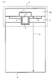
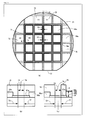
- Fig. 4 shows the structure of a wafer made of polyimide according to this embodiment.
- (a) is a plan view illustrating a main portion
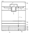
- (b) is a cross-sectional view illustrating the main portion taken along the line X1-X1 of (a)
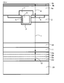
- (c) is a cross-sectional view illustrating the main portion taken along the line X2-X2 of (a).
- polyimide (polyimide in an outer circumferential portion is represented by reference numeral 25 and polyimide which is continuous with the polyimide in the outer circumferential portion and is arranged inside the polyimide is represented by reference numeral 26) is applied with a thickness of about 15 ⁇ m on the entire upper surface of the wafer 1. Then, the polyimide 26 which covers the aluminum electrode 8a of an effective chip 21 and the polyimide 26 on a dicing line 23 which is covered with the insulating film 7a are removed while the polyimide 25 in the outer circumferential portion of the wafer 1 and the polyimide 26 on an ineffective chip 22 remain.
- the insulating film 7a is, for example, a field oxide film or an insulating film which is formed at the same time as the interlayer insulating film 7 is formed.
- a breakdown voltage structure 20 (for example, a RESURF structure) of the effective chip 21 is covered with the insulating film 7a and the insulating film 7a is covered with the polyimide 26.
- the entire breakdown voltage structure 20 is covered with the insulating film 7a, only the emitter electrode 8a of the ineffective chip 22 may be covered, and the emitter electrode 8a and the insulating film 7a of the effective chip 21 may be exposed.
- the breakdown voltage structure 20 when a metal electrode, such as a guard ring, is exposed as the breakdown voltage structure 20, the breakdown voltage structure 20 is also covered with the polyimide 26 in order to prevent the deposition of a plating film on the metal electrode of the breakdown voltage structure 20 and protect the breakdown structure in the subsequent process.
- a metal electrode such as a guard ring
- the effective chip 21 means an available chip when chips are arranged at the center of the wafer 1. Specifically, a chip that is a distance L of 2 mm or more away from the end 25a of the polyimide 25 in the outer circumferential portion is the effective chip 21.
- the ineffective chip 22 means a chip which is arranged in the outer circumference of the wafer 1 and is not available as an element since the edge thereof is chipped off or since a necessary process, such as deposition, is not completely performed.
- a portion in which the polyimide 26 on the dicing line 23 is removed extends to the dicing line 23 interposed between the ineffective chips 22 (reference numeral 28 indicates the extending portion).
- the insulating film 7a is exposed from the removed portion.
- the insulating film 7a is, for example, a BPSG (boron phosphorous glass).
- the width W of the polyimide 25 which is formed in the outer circumferential portion of the wafer 1 from the end 1c of the wafer is equal to or greater than 2 mm.
- the width W is less than 2 mm, silicon or polysilicon is exposed by edge rinse and a plating film is likely to be abnormally deposited on the silicon or polysilicon, as described in the related art.
- the width W is equal to or greater than 5 mm, polysilicon or silicon exposed by edge rinse is reliably coated, which is preferable.
- the width W may be equal to or less than about 10 mm at most.
- the crack (see reference numeral 33 in Fig. 9 ) which occurs during dicing extends to the rear surface of the effective chip 21, which has an adverse effect on the semiconductor device. Therefore, the minimum distance W between the effective chip 21 and the polyimide 25 in the outer circumferential portion is equal to or greater than 2 mm. When the distance W is less than 2 mm, the crack 33 which occurs in the dicing line 23 is likely to reach the effective chip 21.
- the width of the dicing line 23 is, for example, about 80 ⁇ m.
- the crack which occurs in the rear surface of the effective chip 21 will be described below (see Fig. 9 ).
- reference numeral 24 indicates the center line of the dicing line 23 and reference numeral 27 indicates an orientation flat (OF).
- a rear electrode (collector electrode 12) is formed on the rear surface 1b of the wafer 1 by sputtering.
- the collector electrode 12 is a laminated film of an aluminum film 12a (or an aluminum-silicon film)/a titanium film 12b/a nickel film 12c/a gold film 12d from the surface of the wafer 1.
- the collector electrode 12 on the rear surface 1b of the wafer 1 is attached to a glass plate 29.
- the entire laminate is put into an electroless plating layer and the nickel film 8b and the gold film 8c are sequentially formed on the aluminum electrode 8a of the surface of the wafer by electroless plating to form the emitter electrode 8.
- the nickel film 8b and the gold film 8c are formed on the surface of the aluminum electrode 8a since there are needed for soldering to an external lead conductor (external lead wire) .
- process (4) is performed before process (2). In this case, the processes are performed in the order of (1), (4), (2), (3), (5), and (6). In addition, in some cases, process (1) of forming the aluminum electrode 8a is performed after process (3).
- the wafer 1 is diced (cut) into chips along the center line 24 of the dicing line 23 by a blade 32 (diamond cutter) with a diameter of, for example, about 50 mm.
- a cutting width is, for example, about 40 ⁇ m.
- Fig. 7 shows an aspect in which the wafer 1 is diced in a direction indicated by an arrow from the upper side of Fig. 7 to the OF 27.
- reference numeral 31 indicates a dicing tape for attaching the wafer 1.
- the polyimide 26 on a portion from the dicing line 23 to a dicing line (a portion represented by reference numeral 28) interposed between the ineffective chips 22 is removed to prevent a crack (see reference numeral 33 in Fig. 9 ) from occurring in the rear surface of the effective chip 21 as much as possible.
- a crack see reference numeral 33 in Fig. 9
- the occurrence of chipping silicon pieces peel off and are chipped off from the wafer 1 due to the concentration of the crack 33
- the aluminum electrode 8a of the ineffective chip 22 Since polyimide is coated on the aluminum electrode 8a of the ineffective chip 22, the aluminum electrode 8a is not plated. Therefore, the plated region (plating deposition area) is narrowed and it is possible to increase the chemical life of an electroless plating solution. As a result, it is possible to reduce manufacturing costs.
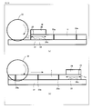
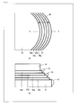
- Fig. 9 is a diagram (part 1) illustrating the state of the crack 33 which occurs in the rear surface of the wafer 1.
- Fig. 9 shows a state in which dicing is performed first along the dicing lines 23 when no dicing has been performed along the horizontal and vertical dicing lines 23.
- (a) is a diagram illustrating a case in which the blade 32 is inserted from the end 1c of the wafer (cutting starts)
- (b) is a diagram illustrating a case in which the blade 32 is separated from the end 1c of the wafer (cutting ends).
- the dicing line 23 interposed between the ineffective chips 22 is covered with the polyimide 25 and the polyimide 26.
- the width W of the polyimide 25 in the outer circumferential portion is 2 mm.
- the emitter electrode 8 or the collector electrode 12 is formed on the wafer 1, but the description thereof will be omitted for simplicity of explanation.
- the crack 33 starts from the end 1c of the wafer and ends in a portion 26a which is disposed immediately below the polyimide.
- the crack 33 starts from a portion (polyimide end 26b) before the portion 26a which is disposed immediately below the polyimide and ends in the portion 26a which is disposed immediately below the polyimide.
- the distance T from the end 26b of the polyimide is less than 2 mm and is generally about 1 mm.
- Fig. 10 is a diagram (part 2) illustrating the state of the crack 33 which occurs in the rear surface of the wafer 1.
- Fig. 10 illustrates the state of the crack 33 which occurs in the rear surface of the wafer 1 when the wafer is cut (diced) by the blade 32 along one of the horizontal and vertical dicing lines 23 and is then cut (diced) along the other dicing lines 23 which have not been cut and are perpendicular to the cut dicing lines 23a (the cut dicing line is represented by 23a).
- the cut dicing line is represented by 23a.
- (a) is a diagram illustrating a case in which the blade 32 is inserted from the end 1c of the wafer (cutting starts) and (b) is a diagram illustrating a case in which the blade 32 is separated from the end 1c of the wafer (cutting ends).
- the crack 33 starts from the end 1c of the wafer and ends in a portion 26a which is disposed immediately below the polyimide.
- the crack 33 starts and ends in the portion 26a which is disposed immediately below the polyimide.
- the crack 33 occurs in the portion 26a which is disposed immediately below the polyimide and does not reach the effective chip 21. Therefore, the crack 33 has no adverse effect on the effective chip 21.
- a position which is away from the portion 26a disposed immediately below the polyimide and where the crack 33 occurs is a position where the blade 32 is separated from the wafer 1 on the dicing line 23 into which the blade 32 is inserted first.
- An example in which the occurrence of the crack 33 is prevented will be described in a second embodiment on the basis of the above.
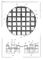
- FIG. 11 is a main process diagram illustrating a method of manufacturing the semiconductor device according to the second embodiment of the invention.
- (a) is a plan view illustrating a main portion
- (b) is a cross-sectional view illustrating the main portion taken along the line X1-X1 of (a)
- (c) is a cross-sectional view illustrating the main portion taken along the line X2-X2 of (a).
- the second embodiment differs from the first embodiment in that, in process (4) described above, the polyimide 26 on the dicing line 23 which is interposed between the ineffective chips 22 in the vicinity of the end of the dicing line 23 into which the blade 32 is inserted first is removed and the polyimide on the dicing lines 23 adjacent to the other ineffective chips 22 remains.
- Fig. 11 numbers (1) to (13) in parentheses indicate a dicing order and an arrow indicates a dicing direction.
- dicing is performed along first to seventh vertical dicing lines 23 ((1) to (7)). This direction is an initial dicing direction.
- dicing is performed along eighth to thirteenth horizontal dicing lines 23 ((8) to (13)).
- the blade 32 is inserted into the upper end of the wafer 1 and the end point of the blade 32 is the OF 27 at the lower end of the wafer 1.
- the polyimide 25 on the dicing line 23 at the end point in the outer circumferential portion remains and the polyimide 26 arranged inside the polyimide 25 is removed (in Fig. 11 , a region B).
- the crack 33 occurs in the portion 26a which is disposed immediately below the polyimide in the outer circumference of the dicing line 23 interposed between the ineffective chips 22 and a portion which is at a distance T of about 1 mm (2 mm or less at most) from the polyimide end 25a.
- the crack 33 which occurs in the portion 1 disposed immediately below the polyimide in the outer circumferential portion does not reach the effective chip 21. Therefore, the crack 33 does not have an adverse effect on the effective chip 21.
- the wafer is diced by the blade 32 along the eighth to thirteenth horizontal dicing lines 23 after the wafer is diced along the first to seventh vertical dicing lines 23a.
- the vertical dicing lines 23a which partition the effective chips 21 and the ineffective chips 22 have already been cut. Therefore, even when the crack 33 occurs in the portion 26a which is disposed immediately below the polyimide by dicing along the eighth to thirteenth horizontal dicing lines, it does not reach the effective chip 21 over the cut dicing lines. As a result, the crack does not have an adverse effect on the effective chip 21.
- a region in which no polyimide is formed such as the region B illustrated in (a) of Fig. 11 , may be not provided on the dicing line which is interposed between the ineffective chips on the cutting end side of the dicing line in a direction perpendicular to the initial cutting direction.
- the second embodiment is an effective method when the position of a portion in which the blade 32 is inserted to dice the wafer 1 is determined or one of the horizontal and vertical dicing lines 23 (23a) to be diced first is determined.
- the vertical direction (direction facing the orientation flat 27) is the initial cutting direction, but the cutting direction is not limited thereto.
- a vertical direction (direction in which cutting starts from the orientation flat 27) opposite to the cutting direction illustrated in Fig. 11 may be the initial cutting direction, or the horizontal direction (direction parallel to the orientation flat 27) may be the initial cutting direction.
- the order of the initial cutting direction and a cutting direction perpendicular to the initial cutting direction may be determined in advance.
- Fig. 12 is a main process diagram illustrating the method of manufacturing the semiconductor device according to the third embodiment of the invention.
- (a) is a plan view illustrating a main portion
- (b) is a cross-sectional view illustrating the main portion taken along the line X1-X1 of (a)
- (c) is a cross-sectional view illustrating the main portion taken along the line X2-X2 of (a).
- the third embodiment differs from the first embodiment in that, in process (4) described above, the aluminum electrode 8a is not formed on the surface of the ineffective chip 22 and the surface of the ineffective chip 22 is covered with the insulating film 7a which extends from the dicing line 23.
- a crack 33 occurs in a portion 26a which is disposed immediately below the polyimide.
- the crack 33 extends inward from a polyimide end 25a, it reaches only a portion that is about 1 mm inside from the polyimide end 25a. Since the effective chip 21 is at a distance of 2 mm or more from the polyimide end 25a, the crack 33 does not reach the effective chip 21 and does not have an adverse effect on the effective chip 21.
- the aluminum electrode 8a is not formed on the ineffective chip 22 and the insulating film 7a is formed on the ineffective chip 22, plating is not performed. Therefore, it is possible to increase the chemical life of an electroless plating solution and reduce manufacturing costs. In addition, since the outer circumferential portion of the wafer 1 is covered with the polyimide 25, abnormal deposition due to electroless plating does not occur.
- the method of manufacturing the semiconductor device according to the invention is applied to manufacture the FS-IGBT.
- the method of manufacturing the semiconductor device according to the invention is not limited to the manufacture of the FS-IGBT.
- the method of manufacturing the semiconductor device according to the invention may be applied to manufacture, for example, IGBTs other than the FS-IGBT, MOSFETs, and diodes.
- the outer circumferential portion of the wafer and the ineffective chips are covered with polyimide and the polyimide on the dicing line interposed between the ineffective chips is removed. In this way, it is possible to prevent the occurrence of a crack in the rear surface of the effective chip due to dicing using the blade.
- the outer circumferential wall of the wafer is covered with polyimide, it is possible to prevent the occurrence of abnormal deposition in the outer circumferential portion of the wafer due to electroless plating.
- the ineffective chips are covered with polyimide, it is possible to prevent the ineffective chips from being plated. Therefore, it is possible to increase the chemical life of a plating solution and reduce manufacturing costs.
- the outer circumferential portion of the wafer is covered with polyimide and the entire upper surface of the ineffective chip is covered with an oxide film, it is possible to prevent the occurrence of a crack in the rear surface of the effective chip due to dicing using the blade and the occurrence of abnormal deposition in the outer circumferential wall of the wafer due to electroless plating.
- the invention relates to a method of manufacturing a semiconductor device and is suitable for, particularly, a semiconductor device manufacturing method for manufacturing a semiconductor wafer (hereinafter, simply referred to as a wafer) using dicing with a blade.
Landscapes
- Internal Circuitry In Semiconductor Integrated Circuit Devices (AREA)
- Dicing (AREA)
- Formation Of Insulating Films (AREA)
Abstract
Description
- The present invention relates to a method of manufacturing a semiconductor device, and more particularly, to a semiconductor device manufacturing method of manufacturing a semiconductor wafer (hereinafter, simply referred to as a wafer) using dicing with a blade.
- In recent years, in power semiconductor devices, such as an IGBT (insulated gate bipolar transistor), a MOSFET (MOS field effect transistor), and a diode which are provided in inverters, the thickness of a silicon substrate for forming the power semiconductor device has been reduced in order to improve the electrical characteristics of the power semiconductor device.
-
Fig. 13 is a diagram illustrating the cross-sectional structure of a main portion of an FS (Field Stop)-IGBT. InFig. 13 , the FS-IGBT includesa p well layer 52 that is provided (formed) in a surface layer of ann silicon substrate 51d (when awafer 51 is cut into chips) with a thickness of about 150 µm and atrench 53 that passes through thep well layer 52. - In addition, the FS-IGBT includes an
n emitter layer 54 that is provided in a surface layer of thep well layer 52 so as to come into contact with thetrench 53. Agate oxide film 55 is provided on the inner wall of thetrench 53 and agate electrode 56 is provided in thetrench 53 through thegate oxide film 55. - An
interlayer insulating film 57 is provided on thegate electrode 56 and anemitter electrode 58 is provided on theinterlayer insulating film 57 so as to be electrically connected to then emitter layer 54. An n-FS layer 60 anda p collector layer 61 are provided on the rear surface of then silicon substrate 51d and acollector electrode 62 is provided on thep collector layer 61 so as to be electrically connected thereto. Next, a process of manufacturing the FS-IGBT will be described. - (1) A surface structure including, for example, the
p well layer 52, then emitter layer 54, thegate electrode 56, and analuminum electrode 58a (which is a front electrode and is a portion of the emitter electrode 58) is formed on the front surface of a thick wafer. Theinterlayer insulating film 57 is formed on thegate electrode 56 and thealuminum electrode 58a is formed on theinterlayer insulating film 57. - (2) A protective tape is attached to the front surface of the thick wafer and the rear surface of the thick wafer is ground. Then, the protective tape peels off and wet etching is performed on a grinding surface to remove a fractured layer. In this way, a
thin wafer 51 with a thickness of about 150 µm is obtained. - (3) Phosphorous (P) and boron (B) ions are implanted into the rear surface and annealing is performed to form an n-
FS layer 60 anda p collector layer 61. - (4)
Polyimide 76 is applied onto the entire upper surface of thewafer 51 and thepolyimide 76 on theemitter electrode 58 of aneffective chip 71 is removed (see (a) ofFig. 14). Fig. 14 is a diagram illustrating a wafer according to the related art. InFig. 14, (a) is a plan view illustrating the wafer according to the related art in which only polyimide on an emitter electrode of an effective chip is removed, (b) is a cross-sectional view illustrating a main portion taken along the line X1-X1 of (a), and (c) is a cross-sectional view illustrating a main portion taken along the line X2-X2 of (a). - In (b) and (c) of
Fig. 14 ,reference numeral 74 indicates the center line of adicing line 73 andreference numeral 57a indicates an insulating film that covers the breakdown voltage structure of an IGBT and thedicing line 73. In addition, in (a) and (c) ofFig. 14 , the leading end of an arrow (a) is the end of the exposed emitter electrode and indicates the emitter-electrode-side end of thepolyimide 76 and the leading end of an arrow (b) is the end of thedicing line 73 and indicates the end of thepolyimide 76. - In the
polyimide 76 which is applied onto the entire upper surface of thewafer 51, when thepolyimide 76 on theemitter electrode 58 of theeffective chip 71 is removed (see (a) ofFig. 14 ), thepolyimide 76 on thedicing line 73 which partition theeffective chips 71 is also removed and theinsulating film 57a on thedicing line 73 is exposed (see (c) ofFig. 14 ). On the other hand, theinsulating film 57a is covered with thepolyimide 76 on thedicing line 73 which partitions the ineffective chips 72 (see (b) ofFig. 14 ). - The
effective chip 71 means an available chip when chips are arranged at the center of thewafer 51. Theineffective chip 72 means a chip which is arranged in the outer circumference of thewafer 51 and is not available as an element since the edge thereof is chipped off or since a necessary process, such as deposition, is not completely performed. - (5) The
collector electrode 62, which is a rear electrode, is formed on the rear surface of thewafer 51 by sputtering. - (6) A
nickel film 58b and agold film 58c are formed only on thealuminum electrode 58a on the surface surrounded by theend 76b of thepolyimide 76 by electroless plating to form the emitter electrode 58 (see (c) ofFig. 14 ). This is needed in order to solder theemitter electrode 58 to an external lead conductor. As illustrated in (c) ofFig. 14 , the polyimide on thedicing line 73 is also removed. However, since theinsulating film 57a is exposed, thenickel film 58b and thegold film 58c are not deposited by electroless plating. - (7) The
wafer 51 is diced into chips along thedicing lines 73 by ablade 82. - Next, the reason why the outer circumferential portion of the
wafer 51 and a portion other than theeffective chips 71 are covered with thepolyimide 76 in the above-mentioned process will be described.Fig. 15 is a diagram illustrating the structure of the wafer subjected to edge rinse andFig. 16 is a diagram illustrating the structure of the wafer on which polyimide is not formed. InFig. 15, (a) is a plan view illustrating a main portion and (b) is a cross-sectional view illustrating the main portion taken along the line X-X of (a). InFig. 15 ,reference numeral 55a indicates an oxide film that is formed at the same time as thegate oxide film 55 is formed,reference numeral 56a indicates a polyimide film that is formed at the same time as thegate electrode 56 is formed,reference numeral 57a indicates an insulating film that is formed at the same time as theinterlayer insulating film 57 is formed, andreference numeral 58d indicates an aluminum film that is formed at the same time as thealuminum electrode 58a is formed. - (Reason 1) As illustrated in
Fig. 15 ,edge rinse 90 is performed on the outer circumferential portion of thewafer 51 and, for example, silicon forming thewafer 51, a polysilicon film for forming thegate electrode 56, and a BPSG film, which is theinterlayer insulating film 57 are exposed from the outer circumferential portion of thewafer 51. Theedge rinse 90 is a process of removing a photoresist which covers the outer circumferential portion of thewafer 51. - As such, when various films formed on the
wafer 51 are exposed from the outer circumferential portion by theedge rinse 90, plating metal is abnormally deposited on a conductive film, such as thepolysilicon film 56a or thealuminum film 58d in the plating process. When anabnormal deposit 91 peels off and is attached to the surface of a semiconductor chip (hereinafter, simply referred to as a chip) during the plating process or in the subsequent process, the reliability of the manufactured semiconductor device, such as an FS-IGBT, is reduced. In order to prevent the reduction in the reliability, the outer circumferential portion of thewafer 51 is covered with thepolyimide 76 such that the outer circumferential portion of thewafer 51 is not plated. - (Reason 2) As illustrated in
Fig. 16 , when the entire surface of thewafer 51 is not covered with thepolyimide 76, thealuminum electrode 58a of theineffective chip 72 is plated with plating metal 92 (for example, a nickel film or a metal film). As a result, the region to be plated increases and the chemical life of a plating solution is reduced, which results in an increase in manufacturing costs. In order to solve the problems, a portion other than theeffective chip 71 is covered with thepolyimide 76. However, theinsulating film 57a covers thebreakdown voltage structure 70 and thedicing line 73. -
Patent Document 1 discloses a technique which forms a passivation film made of a resist on the main surface of a wafer in which a plurality of chips are formed so as to be separated from each other by dicing lines, removes the passivation film on the dicing lines while leaving the passivation film in a region that is several millimeters away from the outer circumferential portion of the wafer, attaches a protective tape to the main surface of the wafer, and grinds the rear surface of the water. In this way, the gap between the dicing line and the protective tape is closed until it reaches the outer circumferential portion of the wafer and the infiltration of abrasive water is prevented when the rear surface of the wafer is ground. Therefore, it is possible to prevent a pad portion of the chip from being contaminated due to Si scrap caused by the mixture of the abrasive water. - Patent Document 1:
JP 2007-36129 A - However, in the above-mentioned technique according to the related art, when the wafer is diced along the
dicing lines 73 by theblade 82, abnormal stress is applied to thewafer 51 in the vicinity of a step portion at theend 76b of thepolyimide 76 and thecrack 83 is likely to occur in the rear surface of thewafer 51 to which thedicing tape 81 is attached (seeFig. 17). Fig. 17 is a diagram illustrating an aspect in which a crack occurs due to polyimide during dicing. InFig. 17, (a) is a plan view illustrating a main portion and (b) is a cross-sectional view illustrating the main portion taken along thedicing line 73. Although not illustrated inFig. 17 , theinsulating film 57a is formed on thedicing line 73 on the front surface of thewafer 51 and thecollector electrode 62, which is a rear electrode, is formed on the rear surface. Thecrack 83 extends to a portion A of theeffective chip 71 and causes the deterioration of the characteristics of theeffective chip 71 or a reduction in the reliability of theeffective chip 71. - Furthermore,
Patent Document 1 discloses a structure in which the outer circumferential portion of the wafer is surrounded by a resist film such that an abrasive solution is not infiltrated into the surface of the wafer when the wafer is thinned. However,Patent Document 1 does not disclose a measure in which a plating film is formed on the front electrode (aluminum electrode) of an element such that a crack caused by polyimide does not occur in the rear surface of the effective chip during dicing. Therefore, the structure disclosed inPatent Document 1 cannot prevent the occurrence of a crack due to polyimide. - In order to solve the above-mentioned problems of the related art, an object of the invention is to provide a method of manufacturing a semiconductor device which can prevent the occurrence of a crack due to polyimide when a wafer is diced along dicing lines by a blade and the abnormal deposition of plating metal in an outer circumferential portion of the wafer and can increase the chemical life of a plating solution to reduce manufacturing costs.
- In order to solve the above-mentioned problems and achieve the object of the invention, a method of manufacturing a semiconductor device according to the invention includes: forming ineffective chips in a circumference of a first main surface of a semiconductor wafer; forming effective chips in a region surrounded by the ineffective chips; forming a front electrode on the effective chips and the ineffective chips; providing an insulating film on dicing lines which partition the effective chips and the ineffective chips; forming a rear electrode on a second main surface of the semiconductor wafer; forming polyimide on an outer circumferential portion of the first main surface of the semiconductor wafer with a predetermined width from an outer circumferential end of the semiconductor wafer such that the polyimide continuously covers the ineffective chips from the outer circumferential end of the semiconductor wafer to the inside and continuously covers a portion which is a predetermined distance away from the outer circumferential end of the semiconductor wafer to the effective chip in the dicing line interposed between the ineffective chips; forming a metal film on the front electrode formed on the effective chips using plating; and cutting the semiconductor wafer into semiconductor chips along the dicing lines using a blade.
- A method of manufacturing a semiconductor device according to the invention includes: forming ineffective chips in a circumference of a first main surface of a semiconductor wafer; forming effective chips in a region surrounded by the ineffective chips; forming a front electrode on the effective chips and the ineffective chips; providing an insulating film on dicing lines which partition the effective chips and the ineffective chips; forming a rear electrode on a second main surface of the semiconductor wafer; forming polyimide on an outer circumferential portion of the first main surface of the semiconductor wafer with a predetermined width from an outer circumferential end of the semiconductor wafer; and forming a metal film on the front electrode formed on the effective chips using plating. In the forming of the polyimide, the polyimide is formed so as to continuously cover the ineffective chip from the outer circumferential end of the semiconductor wafer to the inside. For the dicing line, an initial cutting direction, a direction intersecting the initial cutting direction, and a cutting end side of the initial cutting direction are predetermined. In addition, the polyimide is formed so as to continuously cover a portion which is a predetermined distance away from the outer circumferential end of the semiconductor wafer to the effective chip in the dicing line interposed between the ineffective chips on the cutting end side of the dicing line in the initial cutting direction. The semiconductor wafer is cut into semiconductor chips along the dicing lines in the initial cutting direction by the blade.
- A method of manufacturing a semiconductor device according to the invention includes: forming ineffective chips in a circumference of a first main surface of a semiconductor wafer; forming effective chips in a region surrounded by the ineffective chips; forming a front electrode on the effective chips; forming an insulating film on the ineffective chips; forming the insulating film so as to extend on dicing lines which partition the effective chips and the ineffective chips; forming a rear electrode on a second main surface of the semiconductor wafer; forming polyimide on an outer circumferential portion of the first main surface of the semiconductor wafer with a predetermined width from an outer circumferential end of the semiconductor wafer such that the polyimide continuously covers a portion which is a predetermined distance away from the outer circumferential end of the semiconductor wafer to the effective chip; forming a metal film on the front electrode formed on the effective chips using plating; and cutting the semiconductor wafer into semiconductor chips along the dicing lines using a blade.
- In the method of manufacturing a semiconductor device according to the invention, the predetermined width of the polyimide from the outer circumferential end of the semiconductor wafer may be equal to or greater than 2 mm and equal to or less than 10 mm.
- In the method of manufacturing a semiconductor device according to the invention, the predetermined width of the polyimide from the outer circumferential end of the semiconductor wafer may be equal to or greater than 5 mm and equal to or less than 10 mm.
- In the method of manufacturing a semiconductor device according to the invention, the predetermined distance between the effective chip and the polyimide may be equal to or greater than 2 mm.
- In the method of manufacturing a semiconductor device according to the invention, the front electrode may be an aluminum electrode. The insulating film may be an oxide film. The metal film may be a plating film obtained by forming a gold film on a nickel film. The plating may be electroless plating. The main electrode may be a laminated film of an aluminum film, a nickel film, and a gold film.
-
-
Fig. 1 is a diagram (part 1) illustrating a process of manufacturing a main portion of a semiconductor device according to a first embodiment of the invention. -
Fig. 2 is a diagram (part 2) illustrating the process of manufacturing the main portion of the semiconductor device according to the first embodiment of the invention. -
Fig. 3 is a diagram (part 3) illustrating the process of manufacturing the main portion of the semiconductor device according to the first embodiment of the invention. -
Fig. 4 is a diagram (part 4) illustrating the process of manufacturing the main portion of the semiconductor device according to the first embodiment of the invention. -
Fig. 5 is a diagram (part 5) illustrating the process of manufacturing the main portion of the semiconductor device according to the first embodiment of the invention. -
Fig. 6 is a diagram (part 6) illustrating the process of manufacturing the main portion of the semiconductor device according to the first embodiment of the invention. -
Fig. 7 is a diagram (part 7) illustrating the process of manufacturing the main portion of the semiconductor device according to the first embodiment of the invention. -
Fig. 8 is a diagram illustrating the cross-section of the main portion (cell) of the semiconductor device according to the first embodiment of the invention. -
Fig. 9 is a diagram (part 1) illustrating the state of a crack which occurs in a rear surface of a wafer. -
Fig. 10 is a diagram (part 2) illustrating the state of the crack which occurs in the rear surface of the wafer. -
Fig. 11 is a main process diagram illustrating a method of manufacturing a main portion of a semiconductor device according to a second embodiment of the invention. -
Fig. 12 is a main process diagram illustrating a method of manufacturing a main portion of a semiconductor device according to a third embodiment of the invention. -
Fig. 13 is a diagram illustrating the cross-sectional structure of a main portion of an FS-IGBT. -
Fig. 14 is a diagram illustrating a wafer according to the related art. -
Fig. 15 is a diagram illustrating the structure of the wafer subjected to edge rinse. -
Fig. 16 is a diagram illustrating the structure of a wafer on which polyimide is not formed. -
Fig. 17 is a diagram illustrating an aspect in which a crack occurs due to polyimide during dicing. - Hereinafter, methods of manufacturing semiconductor devices according to exemplary embodiments of the invention will be described in detail with reference to the accompanying drawings. In the following description of the embodiments and the accompanying drawings, the same components are denoted by the same reference numerals and the description thereof will not be repeated.
- First, a method of manufacturing a semiconductor device according to a first embodiment of the invention will be described.
Fig. 1 ,Fig. 2 ,Fig. 3 ,Fig. 4 ,Fig. 5 ,Fig. 6 , andFig. 7 are diagrams illustrating a process of manufacturing a main portion of the semiconductor device according to the first embodiment of the invention.Fig. 8 is a diagram illustrating the cross-section of the main portion (cell) of the semiconductor device according to the first embodiment of the invention.Figs. 1 to 7 show the main portion of the semiconductor device manufactured by the semiconductor device manufacturing method according to the first embodiment of the invention in the order of processes.Fig. 8 shows an FS-IGBT as an example of the semiconductor device according to the first embodiment of the invention. The structure of the FS-IGBT is the same as that of the FS-IGBT illustrated inFig. 14 and thus the detailed description thereof will not be repeated. - In
Figs. 1 to 8 ,reference numeral 1a indicates an n silicon substrate (wafer 1),reference numeral 2 indicates a p well layer,reference numeral 3 indicates a trench,reference numeral 4 indicates an n emitter layer,reference numeral 5 indicates a gate oxide film,reference numeral 6 indicates a gate electrode,reference numeral 7 indicates an interlayer insulating film,reference numeral 8 indicates an emitter electrode,reference numeral 8a indicates an aluminum electrode,reference numeral 8b indicates a nickel film,reference numeral 8c indicates a gold film,reference numeral 10 indicates an n-FS layer,reference numeral 11 indicates a p collector layer, andreference numeral 12 indicates a collector electrode. However,Fig. 8 does not show a gate pad. Theemitter electrode 8 includes thealuminum electrode 8a, and thenickel film 8b and thegold film 8c that cover thealuminum electrode 8a. Next, a process of manufacturing the FS-IGBT illustrated inFig. 8 will be described with reference toFigs. 1 to 7 . - (1) As illustrated in
Fig. 1 , asurface structure 9 including, for example, thep well layer 2, then emitter layer 4, thegate electrode 6, and thealuminum electrode 8a (which is a front electrode and is a portion of the emitter electrode 8) is formed on the front surface of ann silicon substrate 1a (wafer 1). Theinterlayer insulating film 7 is formed between thegate electrode 6 and thealuminum electrode 8a. Thealuminum electrode 8a may be made of an aluminum-silicon (Al-Si) film or an aluminum-silicon-copper (Al-Si-Cu) film other than an aluminum (Al) film. - (2) As illustrated in
Fig. 2 , aprotective tape 9a is attached to the surface of the surface structure, arear surface 1b is ground, and theprotective tape 9a peels off. In addition, wet etching is performed on the ground surface. A thick wafer (n silicon substrate) 1a is changed into athin wafer 1 with a thickness of, for example, about 150 µm by the wet etching. The thickness varies depending on the breakdown voltage of the FS-IGBT. - (3) As illustrated in
Fig. 3 , phosphorous and boron ions are implanted into therear surface 1b annealing is performed to form the n-FS layer 10 and thep collector layer 11. - (4)
Fig. 4 shows the structure of a wafer made of polyimide according to this embodiment. InFig. 4, (a) is a plan view illustrating a main portion, (b) is a cross-sectional view illustrating the main portion taken along the line X1-X1 of (a), and (c) is a cross-sectional view illustrating the main portion taken along the line X2-X2 of (a). As illustrated inFig. 4 , polyimide (polyimide in an outer circumferential portion is represented byreference numeral 25 and polyimide which is continuous with the polyimide in the outer circumferential portion and is arranged inside the polyimide is represented by reference numeral 26) is applied with a thickness of about 15 µm on the entire upper surface of thewafer 1. Then, thepolyimide 26 which covers thealuminum electrode 8a of aneffective chip 21 and thepolyimide 26 on adicing line 23 which is covered with the insulatingfilm 7a are removed while thepolyimide 25 in the outer circumferential portion of thewafer 1 and thepolyimide 26 on anineffective chip 22 remain. The insulatingfilm 7a is, for example, a field oxide film or an insulating film which is formed at the same time as theinterlayer insulating film 7 is formed. - In (b) of
Fig. 4 , in some cases, a breakdown voltage structure 20 (for example, a RESURF structure) of theeffective chip 21 is covered with the insulatingfilm 7a and the insulatingfilm 7a is covered with thepolyimide 26. However, as illustrated inFig. 4 , when the entirebreakdown voltage structure 20 is covered with the insulatingfilm 7a, only theemitter electrode 8a of theineffective chip 22 may be covered, and theemitter electrode 8a and the insulatingfilm 7a of theeffective chip 21 may be exposed. Although not illustrated in the drawings, when a metal electrode, such as a guard ring, is exposed as thebreakdown voltage structure 20, thebreakdown voltage structure 20 is also covered with thepolyimide 26 in order to prevent the deposition of a plating film on the metal electrode of thebreakdown voltage structure 20 and protect the breakdown structure in the subsequent process. - The
effective chip 21 means an available chip when chips are arranged at the center of thewafer 1. Specifically, a chip that is a distance L of 2 mm or more away from theend 25a of thepolyimide 25 in the outer circumferential portion is theeffective chip 21. Theineffective chip 22 means a chip which is arranged in the outer circumference of thewafer 1 and is not available as an element since the edge thereof is chipped off or since a necessary process, such as deposition, is not completely performed. - A portion in which the
polyimide 26 on the dicingline 23 is removed extends to the dicingline 23 interposed between the ineffective chips 22 (reference numeral 28 indicates the extending portion). The insulatingfilm 7a is exposed from the removed portion. The insulatingfilm 7a is, for example, a BPSG (boron phosphorous glass). - The width W of the
polyimide 25 which is formed in the outer circumferential portion of thewafer 1 from theend 1c of the wafer is equal to or greater than 2 mm. When the width W is less than 2 mm, silicon or polysilicon is exposed by edge rinse and a plating film is likely to be abnormally deposited on the silicon or polysilicon, as described in the related art. When the width W is equal to or greater than 5 mm, polysilicon or silicon exposed by edge rinse is reliably coated, which is preferable. When the width W is too large, the number ofeffective chips 21 is reduced. Therefore, the width W may be equal to or less than about 10 mm at most. - In some cases, the crack (see
reference numeral 33 inFig. 9 ) which occurs during dicing extends to the rear surface of theeffective chip 21, which has an adverse effect on the semiconductor device. Therefore, the minimum distance W between theeffective chip 21 and thepolyimide 25 in the outer circumferential portion is equal to or greater than 2 mm. When the distance W is less than 2 mm, thecrack 33 which occurs in the dicingline 23 is likely to reach theeffective chip 21. The width of the dicingline 23 is, for example, about 80 µm. The crack which occurs in the rear surface of theeffective chip 21 will be described below (seeFig. 9 ). InFig. 4 ,reference numeral 24 indicates the center line of the dicingline 23 andreference numeral 27 indicates an orientation flat (OF). - (5) As illustrated in
Fig. 5 , a rear electrode (collector electrode 12) is formed on therear surface 1b of thewafer 1 by sputtering. Thecollector electrode 12 is a laminated film of analuminum film 12a (or an aluminum-silicon film)/atitanium film 12b/anickel film 12c/agold film 12d from the surface of thewafer 1. - (6) As illustrated in
Fig. 6 , thecollector electrode 12 on therear surface 1b of thewafer 1 is attached to aglass plate 29. The entire laminate is put into an electroless plating layer and thenickel film 8b and thegold film 8c are sequentially formed on thealuminum electrode 8a of the surface of the wafer by electroless plating to form theemitter electrode 8. Thenickel film 8b and thegold film 8c are formed on the surface of thealuminum electrode 8a since there are needed for soldering to an external lead conductor (external lead wire) . - In some cases, process (4) is performed before process (2). In this case, the processes are performed in the order of (1), (4), (2), (3), (5), and (6). In addition, in some cases, process (1) of forming the
aluminum electrode 8a is performed after process (3). - (7) As illustrated in
Fig. 7 , thewafer 1 is diced (cut) into chips along thecenter line 24 of the dicingline 23 by a blade 32 (diamond cutter) with a diameter of, for example, about 50 mm. When the wafer is diced along the dicingline 23 by the edge of theblade 32, a cutting width (dicing width) is, for example, about 40 µm.Fig. 7 shows an aspect in which thewafer 1 is diced in a direction indicated by an arrow from the upper side ofFig. 7 to theOF 27. InFig. 7 ,reference numeral 31 indicates a dicing tape for attaching thewafer 1. - As illustrated in
Fig. 4 , thepolyimide 26 on a portion from the dicingline 23 to a dicing line (a portion represented by reference numeral 28) interposed between theineffective chips 22 is removed to prevent a crack (seereference numeral 33 inFig. 9 ) from occurring in the rear surface of theeffective chip 21 as much as possible. When the occurrence of thecrack 33 is prevented, the occurrence of chipping (silicon pieces peel off and are chipped off from thewafer 1 due to the concentration of the crack 33) is also prevented. - Since polyimide is coated on the
aluminum electrode 8a of theineffective chip 22, thealuminum electrode 8a is not plated. Therefore, the plated region (plating deposition area) is narrowed and it is possible to increase the chemical life of an electroless plating solution. As a result, it is possible to reduce manufacturing costs. - Since the outer circumferential portion of the
wafer 1 is covered with thepolyimide 25, silicon or polysilicon which is exposed by edge rinse is covered with thepolyimide 25. As a result, abnormal plating deposition in the outer circumferential portion of thewafer 1 is prevented. In addition, since the outer circumferential portion of thewafer 1 is covered with thepolyimide 25, the occurrence of thecrack 33 is prevented. Therefore, the strength of the chip is improved and it is possible to improve the reliability of products. - Next, the detailed investigation result of the state of the
crack 33 which occurs in the rear surface of thewafer 1 when thewafer 1 is diced in the polyimide pattern illustrated inFig. 14 according to the related art will be described. For the pattern of thepolyimide 26, thepolyimide 26 on the dicingline 23 interposed between theineffective chips 22 is also covered. Therefore, inFig. 9 ,reference numeral 26b corresponds to reference numeral 76b inFig. 14 . -
Fig. 9 is a diagram (part 1) illustrating the state of thecrack 33 which occurs in the rear surface of thewafer 1.Fig. 9 shows a state in which dicing is performed first along the dicinglines 23 when no dicing has been performed along the horizontal and vertical dicing lines 23. InFig. 9, (a) is a diagram illustrating a case in which theblade 32 is inserted from theend 1c of the wafer (cutting starts) and (b) is a diagram illustrating a case in which theblade 32 is separated from theend 1c of the wafer (cutting ends). The dicingline 23 interposed between theineffective chips 22 is covered with thepolyimide 25 and thepolyimide 26. In addition, the width W of thepolyimide 25 in the outer circumferential portion is 2 mm. Theemitter electrode 8 or thecollector electrode 12 is formed on thewafer 1, but the description thereof will be omitted for simplicity of explanation. - As illustrated in (a) of
Fig. 9 , thecrack 33 starts from theend 1c of the wafer and ends in aportion 26a which is disposed immediately below the polyimide. In addition, as illustrated in (b) ofFig. 9 , thecrack 33 starts from a portion (polyimide end 26b) before theportion 26a which is disposed immediately below the polyimide and ends in theportion 26a which is disposed immediately below the polyimide. The distance T from theend 26b of the polyimide is less than 2 mm and is generally about 1 mm. - In (a) of
Fig. 9 , since thecrack 33 occurs in theportion 26a which is disposed immediately below the polyimide, thecrack 33 does not extend to theeffective chip 21. On the other hand, as illustrated in (b) ofFig. 9 , when thecrack 32 starts before theportion 26a which is disposed immediately below the polyimide and theeffective chip 21 approaches thepolyimide 26 on the dicingline 23, thecrack 33 is likely to extend to the rear surface of theeffective chip 21. -
Fig. 10 is a diagram (part 2) illustrating the state of thecrack 33 which occurs in the rear surface of thewafer 1.Fig. 10 illustrates the state of thecrack 33 which occurs in the rear surface of thewafer 1 when the wafer is cut (diced) by theblade 32 along one of the horizontal andvertical dicing lines 23 and is then cut (diced) along theother dicing lines 23 which have not been cut and are perpendicular to thecut dicing lines 23a (the cut dicing line is represented by 23a). InFig. 10, (a) is a diagram illustrating a case in which theblade 32 is inserted from theend 1c of the wafer (cutting starts) and (b) is a diagram illustrating a case in which theblade 32 is separated from theend 1c of the wafer (cutting ends). - As illustrated in (a) of
Fig. 10 , thecrack 33 starts from theend 1c of the wafer and ends in aportion 26a which is disposed immediately below the polyimide. In addition, as illustrated in (b) ofFig. 10 , thecrack 33 starts and ends in theportion 26a which is disposed immediately below the polyimide. InFig. 10 , in both cases, thecrack 33 occurs in theportion 26a which is disposed immediately below the polyimide and does not reach theeffective chip 21. Therefore, thecrack 33 has no adverse effect on theeffective chip 21. - As can be seen from the above, a position which is away from the
portion 26a disposed immediately below the polyimide and where thecrack 33 occurs is a position where theblade 32 is separated from thewafer 1 on the dicingline 23 into which theblade 32 is inserted first. An example in which the occurrence of thecrack 33 is prevented will be described in a second embodiment on the basis of the above. - Next, a method of manufacturing a semiconductor device according to the second embodiment of the invention will be described.
Fig. 11 is a main process diagram illustrating a method of manufacturing the semiconductor device according to the second embodiment of the invention. InFig. 11, (a) is a plan view illustrating a main portion, (b) is a cross-sectional view illustrating the main portion taken along the line X1-X1 of (a), and (c) is a cross-sectional view illustrating the main portion taken along the line X2-X2 of (a). - The second embodiment differs from the first embodiment in that, in process (4) described above, the
polyimide 26 on the dicingline 23 which is interposed between theineffective chips 22 in the vicinity of the end of the dicingline 23 into which theblade 32 is inserted first is removed and the polyimide on the dicing lines 23 adjacent to the otherineffective chips 22 remains. - In
Fig. 11 , numbers (1) to (13) in parentheses indicate a dicing order and an arrow indicates a dicing direction. First, dicing is performed along first to seventh vertical dicing lines 23 ((1) to (7)). This direction is an initial dicing direction. Then, dicing is performed along eighth to thirteenth horizontal dicing lines 23 ((8) to (13)). In the first to seventhvertical dicing lines 23, theblade 32 is inserted into the upper end of thewafer 1 and the end point of theblade 32 is theOF 27 at the lower end of thewafer 1. Thepolyimide 25 on the dicingline 23 at the end point in the outer circumferential portion remains and thepolyimide 26 arranged inside thepolyimide 25 is removed (inFig. 11 , a region B). - Since the
polyimide 26 is not formed on the dicing lines 23 (portion B) on the cutting end side of theblade 32 except for thepolyimide 25 in the outer circumferential portion, thecrack 33 occurs in theportion 26a which is disposed immediately below the polyimide in the outer circumference of the dicingline 23 interposed between theineffective chips 22 and a portion which is at a distance T of about 1 mm (2 mm or less at most) from thepolyimide end 25a. - Since the
effective chip 21 is at a distance of 2 mm or more from thepolyimide end 25a (distance L inFig. 4 ), thecrack 33 which occurs in theportion 1 disposed immediately below the polyimide in the outer circumferential portion does not reach theeffective chip 21. Therefore, thecrack 33 does not have an adverse effect on theeffective chip 21. - The wafer is diced by the
blade 32 along the eighth to thirteenthhorizontal dicing lines 23 after the wafer is diced along the first to seventhvertical dicing lines 23a. At that time, thevertical dicing lines 23a which partition theeffective chips 21 and theineffective chips 22 have already been cut. Therefore, even when thecrack 33 occurs in theportion 26a which is disposed immediately below the polyimide by dicing along the eighth to thirteenth horizontal dicing lines, it does not reach theeffective chip 21 over the cut dicing lines. As a result, the crack does not have an adverse effect on theeffective chip 21. - Therefore, a region in which no polyimide is formed, such as the region B illustrated in (a) of
Fig. 11 , may be not provided on the dicing line which is interposed between the ineffective chips on the cutting end side of the dicing line in a direction perpendicular to the initial cutting direction. - The second embodiment is an effective method when the position of a portion in which the
blade 32 is inserted to dice thewafer 1 is determined or one of the horizontal and vertical dicing lines 23 (23a) to be diced first is determined. - In the above-described embodiment, the vertical direction (direction facing the orientation flat 27) is the initial cutting direction, but the cutting direction is not limited thereto. A vertical direction (direction in which cutting starts from the orientation flat 27) opposite to the cutting direction illustrated in
Fig. 11 may be the initial cutting direction, or the horizontal direction (direction parallel to the orientation flat 27) may be the initial cutting direction. Alternatively, when the chips are arranged so as to be inclined with respect to the orientation flat 27, the order of the initial cutting direction and a cutting direction perpendicular to the initial cutting direction may be determined in advance. - As described above, when the initial cutting direction is determined in advance, for the dicing line arranged in the initial cutting direction, a portion, which is at a predetermined distance from the outer circumferential end of the semiconductor wafer with respect to the effective chip, in the dicing line interposed between the ineffective chips on the cutting end side is continuously covered. In other words, no polyimide is formed on the portion, which is at a predetermined distance from the effective chip, in the dicing line interposed between the ineffective chips on the cutting side. When the order of the cutting direction is not determined in advance, the method according to the first embodiment may be applied.
- Next, a method of manufacturing a semiconductor device according to a third embodiment of the invention will be described.
Fig. 12 is a main process diagram illustrating the method of manufacturing the semiconductor device according to the third embodiment of the invention. InFig. 12, (a) is a plan view illustrating a main portion, (b) is a cross-sectional view illustrating the main portion taken along the line X1-X1 of (a), and (c) is a cross-sectional view illustrating the main portion taken along the line X2-X2 of (a). The third embodiment differs from the first embodiment in that, in process (4) described above, thealuminum electrode 8a is not formed on the surface of theineffective chip 22 and the surface of theineffective chip 22 is covered with the insulatingfilm 7a which extends from the dicingline 23. - According to the method of manufacturing the semiconductor device according to the third embodiment of the invention, in process (4) described above, only the outer circumferential portion of the
wafer 1 is covered with thepolyimide 25. Therefore, acrack 33 occurs in aportion 26a which is disposed immediately below the polyimide. However, even when thecrack 33 extends inward from apolyimide end 25a, it reaches only a portion that is about 1 mm inside from thepolyimide end 25a. Since theeffective chip 21 is at a distance of 2 mm or more from thepolyimide end 25a, thecrack 33 does not reach theeffective chip 21 and does not have an adverse effect on theeffective chip 21. - Since the
aluminum electrode 8a is not formed on theineffective chip 22 and the insulatingfilm 7a is formed on theineffective chip 22, plating is not performed. Therefore, it is possible to increase the chemical life of an electroless plating solution and reduce manufacturing costs. In addition, since the outer circumferential portion of thewafer 1 is covered with thepolyimide 25, abnormal deposition due to electroless plating does not occur. - In the above-described first to third embodiments, the method of manufacturing the semiconductor device according to the invention is applied to manufacture the FS-IGBT. However, the method of manufacturing the semiconductor device according to the invention is not limited to the manufacture of the FS-IGBT. The method of manufacturing the semiconductor device according to the invention may be applied to manufacture, for example, IGBTs other than the FS-IGBT, MOSFETs, and diodes.
- As described above, according to the invention, the outer circumferential portion of the wafer and the ineffective chips are covered with polyimide and the polyimide on the dicing line interposed between the ineffective chips is removed. In this way, it is possible to prevent the occurrence of a crack in the rear surface of the effective chip due to dicing using the blade.
- According to the invention, since the outer circumferential wall of the wafer is covered with polyimide, it is possible to prevent the occurrence of abnormal deposition in the outer circumferential portion of the wafer due to electroless plating.
- According to the invention, since the ineffective chips are covered with polyimide, it is possible to prevent the ineffective chips from being plated. Therefore, it is possible to increase the chemical life of a plating solution and reduce manufacturing costs.
- According to the invention, since the outer circumferential portion of the wafer is covered with polyimide and the entire upper surface of the ineffective chip is covered with an oxide film, it is possible to prevent the occurrence of a crack in the rear surface of the effective chip due to dicing using the blade and the occurrence of abnormal deposition in the outer circumferential wall of the wafer due to electroless plating. In addition, it is possible to increase the chemical life of a plating solution and reduce manufacturing costs.
- As described above, the invention relates to a method of manufacturing a semiconductor device and is suitable for, particularly, a semiconductor device manufacturing method for manufacturing a semiconductor wafer (hereinafter, simply referred to as a wafer) using dicing with a blade.
-
- 1
- WAFER (THIN)
- 1a
- WAFER (THICK)
- 1b
- REAR SURFACE OF WAFER
- 1c
- END OF WAFER
- 2
- p WELL LAYER
- 3
- TRENCH
- 4
- n EMITTER LAYER
- 5
- GATE OXIDE FILM
- 6
- GATE ELECTRODE
- 7
- INTERLAYER INSULATING FILM
- 7a
- INSULATING FILM
- 8
- EMITTER ELECTRODE
- 8a
- ALUMINUM ELECTRODE
- 8b
- NICKEL FILM
- 8c
- GOLD FILM
- 9
- SURFACE STRUCTURE
- 10
- n-FS LAYER
- 11
- p COLLECTOR LAYER
- 12
- COLLECTOR ELECTRODE
- 12a
- ALUMINUM FILM
- 12b
- TITANIUM FILM
- 12c
- NICKEL FILM
- 12d
- GOLD FILM
- 20
- BREAKDOWN VOLTAGE STRUCTURE
- 21
- EFFECTIVE CHIP
- 22
- INEFFECTIVE CHIP
- 23
- DICING LINE
- 24
- CENTER LINE
- 25
- POLYIMIDE (OUTER CIRCUMFERENTIAL PORTION)
- 25a
- END OF
POLYIMIDE 25 - 26
- POLYIMIDE (INSIDE)
- 26a
- PORTION DISPOSED IMMEDIATELY BELOW POLYIMIDE
- 26b
- END OF
POLYIMIDE 26 - 27
- ORIENTATION FLAT (OF)
- 28
- EXTENDING PORTION
- 29
- GLASS PLATE
- 31
- DICING TAPE
- 32
- BLADE
- 33
- CRACK
Claims (7)
- A method of manufacturing a semiconductor device comprising:forming ineffective chips in a circumference of a first main surface of a semiconductor wafer;forming effective chips in a region surrounded by the ineffective chips;forming a front electrode on the effective chips and the ineffective chips;providing an insulating film on dicing lines which partition the effective chips and the ineffective chips;forming a rear electrode on a second main surface of the semiconductor wafer;forming polyimide on an outer circumferential portion of the first main surface of the semiconductor wafer with a predetermined width from an outer circumferential end of the semiconductor wafer such that the polyimide continuously covers the ineffective chips from the outer circumferential end of the semiconductor wafer to the inside and continuously covers a portion which is a predetermined distance away from the outer circumferential end of the semiconductor wafer to the effective chip in the dicing line interposed between the ineffective chips;forming a metal film on the front electrode formed on the effective chips using plating; andcutting the semiconductor wafer into semiconductor chips along the dicing lines using a blade.
- A method of manufacturing a semiconductor device comprising:forming ineffective chips in a circumference of a first main surface of a semiconductor wafer;forming effective chips in a region surrounded by the ineffective chips;forming a front electrode on the effective chips and the ineffective chips;providing an insulating film on dicing lines which partition the effective chips and the ineffective chips;forming a rear electrode on a second main surface of the semiconductor wafer;forming polyimide on an outer circumferential portion of the first main surface of the semiconductor wafer with a predetermined width from an outer circumferential end of the semiconductor wafer; andforming a metal film on the front electrode formed on the effective chips using plating,wherein, in the forming of the polyimide, the polyimide is formed so as to continuously cover the ineffective chip from the outer circumferential end of the semiconductor wafer to the inside,for the dicing line, an initial cutting direction, a direction intersecting the initial cutting direction, and a cutting end side of the initial cutting direction are predetermined,the polyimide is formed so as to continuously cover a portion which is a predetermined distance away from the outer circumferential end of the semiconductor wafer to the effective chip in the dicing line interposed between the ineffective chips on the cutting end side of the dicing line in the initial cutting direction, andthe semiconductor wafer is cut into semiconductor chips along the dicing lines in the initial cutting direction by the blade.
- A method of manufacturing a semiconductor device comprising:forming ineffective chips in a circumference of a first main surface of a semiconductor wafer;forming effective chips in a region surrounded by the ineffective chips;forming a front electrode on the effective chips;forming an insulating film on the ineffective chips;forming the insulating film so as to extend on dicing lines which partition the effective chips and the ineffective chipsforming a rear electrode on a second main surface of the semiconductor wafer;forming polyimide on an outer circumferential portion of the first main surface of the semiconductor wafer with a predetermined width from an outer circumferential end of the semiconductor wafer such that the polyimide continuously covers a portion which is a predetermined distance away from the outer circumferential end of the semiconductor wafer to the effective chip;forming a metal film on the front electrode formed on the effective chips using plating; andcutting the semiconductor wafer into semiconductor chips along the dicing lines using a blade.
- The method of manufacturing a semiconductor device according to any one of claims 1 to 3,
wherein the predetermined width of the polyimide from the outer circumferential end of the semiconductor wafer is equal to or greater than 2 mm and equal to or less than 10 mm. - The method of manufacturing a semiconductor device according to any one of claims 1 to 3,
wherein the predetermined width of the polyimide from the outer circumferential end of the semiconductor wafer is equal to or greater than 5 mm and equal to or less than 10 mm. - The method of manufacturing a semiconductor device according to any one of claims 1 to 3,
wherein the predetermined distance between the effective chip and the polyimide is equal to or greater than 2 mm. - The method of manufacturing a semiconductor device according to any one of claims 1 to 3,
wherein the front electrode is an aluminum electrode, the insulating film is an oxide film,
the metal film is a plating film obtained by forming a gold film on a nickel film,
the plating is electroless plating, and
the main electrode is a laminated film of an aluminum film, a nickel film, and a gold film.
Applications Claiming Priority (2)
| Application Number | Priority Date | Filing Date | Title |
|---|---|---|---|
| JP2010211487 | 2010-09-22 | ||
| PCT/JP2011/071408 WO2012039403A1 (en) | 2010-09-22 | 2011-09-20 | Method for manufacturing semiconductor device |
Publications (3)
| Publication Number | Publication Date |
|---|---|
| EP2587525A1 true EP2587525A1 (en) | 2013-05-01 |
| EP2587525A4 EP2587525A4 (en) | 2017-07-26 |
| EP2587525B1 EP2587525B1 (en) | 2020-03-25 |
Family
ID=45873887
Family Applications (1)
| Application Number | Title | Priority Date | Filing Date |
|---|---|---|---|
| EP11826848.1A Active EP2587525B1 (en) | 2010-09-22 | 2011-09-20 | Method of manufacturing semiconductor device |
Country Status (5)
| Country | Link |
|---|---|
| US (1) | US8865567B2 (en) |
| EP (1) | EP2587525B1 (en) |
| JP (1) | JP5609981B2 (en) |
| CN (1) | CN103069546B (en) |
| WO (1) | WO2012039403A1 (en) |
Families Citing this family (8)
| Publication number | Priority date | Publication date | Assignee | Title |
|---|---|---|---|---|
| JP6265594B2 (en) | 2012-12-21 | 2018-01-24 | ラピスセミコンダクタ株式会社 | Semiconductor device manufacturing method and semiconductor device |
| USD720313S1 (en) * | 2014-06-16 | 2014-12-30 | Emcore Solar Power, Inc. | Semiconductor wafer with dicing positions for solar cell fabrication |
| TWD174921S (en) * | 2014-12-17 | 2016-04-11 | 日本碍子股份有限公司 | Portion of composite substrates |
| JP6770443B2 (en) * | 2017-01-10 | 2020-10-14 | ルネサスエレクトロニクス株式会社 | Manufacturing method of semiconductor devices and semiconductor wafers |
| CN109616414A (en) * | 2018-11-06 | 2019-04-12 | 深圳方正微电子有限公司 | Wafer processing method and preparation method of semiconductor device |
| KR102935507B1 (en) | 2020-08-20 | 2026-03-06 | 삼성전자주식회사 | Semiconductor substrate and method of sawing a semiconductor substrate |
| USD1118897S1 (en) | 2021-09-08 | 2026-03-17 | Lam Research Corporation | Debubbler component |
| JP7638197B2 (en) | 2021-11-19 | 2025-03-03 | 三菱電機株式会社 | Semiconductor wafer and method for manufacturing the same |
Family Cites Families (7)
| Publication number | Priority date | Publication date | Assignee | Title |
|---|---|---|---|---|
| JPH05315304A (en) * | 1992-05-12 | 1993-11-26 | Sony Corp | Method for polishing back of wafer |
| JP3094939B2 (en) * | 1997-03-19 | 2000-10-03 | 株式会社村田製作所 | Electronic component manufacturing method |
| JP3829860B2 (en) * | 2004-01-30 | 2006-10-04 | 株式会社デンソー | Manufacturing method of semiconductor chip |
| JP4165467B2 (en) * | 2004-07-12 | 2008-10-15 | セイコーエプソン株式会社 | Dicing sheet and method for manufacturing semiconductor device |
| JP2007036129A (en) * | 2005-07-29 | 2007-02-08 | Renesas Technology Corp | Manufacturing method of semiconductor device |
| JP2007214268A (en) * | 2006-02-08 | 2007-08-23 | Seiko Instruments Inc | Manufacturing method of semiconductor device |
| JP2007287780A (en) * | 2006-04-13 | 2007-11-01 | Toshiba Corp | Semiconductor device manufacturing method and semiconductor device |
-
2011
- 2011-09-20 WO PCT/JP2011/071408 patent/WO2012039403A1/en not_active Ceased
- 2011-09-20 JP JP2012535042A patent/JP5609981B2/en active Active
- 2011-09-20 CN CN201180039092.9A patent/CN103069546B/en active Active
- 2011-09-20 EP EP11826848.1A patent/EP2587525B1/en active Active
- 2011-09-20 US US13/817,112 patent/US8865567B2/en active Active
Non-Patent Citations (1)
| Title |
|---|
| See references of WO2012039403A1 * |
Also Published As
| Publication number | Publication date |
|---|---|
| US8865567B2 (en) | 2014-10-21 |
| WO2012039403A1 (en) | 2012-03-29 |
| CN103069546B (en) | 2016-05-04 |
| EP2587525B1 (en) | 2020-03-25 |
| EP2587525A4 (en) | 2017-07-26 |
| JP5609981B2 (en) | 2014-10-22 |
| US20130203238A1 (en) | 2013-08-08 |
| CN103069546A (en) | 2013-04-24 |
| JPWO2012039403A1 (en) | 2014-02-03 |
Similar Documents
| Publication | Publication Date | Title |
|---|---|---|
| EP2587525B1 (en) | Method of manufacturing semiconductor device | |
| US10741504B2 (en) | Semiconductor device manufacturing method and semiconductor wafer | |
| US20170110452A1 (en) | Method of manufacturing a semiconductor device having reduced on-state resistance and structure | |
| CN103839910B (en) | The method of semiconductor apparatus assembly, semiconductor wafer and manufacture semiconductor devices including chip carrier | |
| EP2950338A1 (en) | Dicing method for wafer-level packaging and semiconductor chip with dicing structure adapted for wafer-level packaging | |
| JP2016018952A (en) | Semiconductor device manufacturing method and semiconductor device | |
| CN206639796U (en) | Semiconductor devices | |
| US20170162458A1 (en) | Method for manufacturing semiconductor device | |
| US11658093B2 (en) | Semiconductor element with electrode having first section and second sections in contact with the first section, and semiconductor device | |
| JP3620528B2 (en) | Manufacturing method of semiconductor device | |
| US9543154B2 (en) | Method for manufacturing semiconductor device | |
| EP1952435A1 (en) | Semiconductor wafer including semiconductor chips divided by scribe line and process-monitor electrode pads formed on scribe line | |
| JP2025085827A (en) | Semiconductor Device | |
| EP2927961A1 (en) | Semiconductor device | |
| US20160064325A1 (en) | Semiconductor device and structure therefor | |
| US10403497B2 (en) | Method of manufacturing silicon carbide semiconductor device and silicon carbide semiconductor device | |
| US20180144982A1 (en) | Semiconductor devices and methods for manufacturing semiconductor devices | |
| US11270948B2 (en) | Semiconductor wafer, semiconductor chip and method of fabricating a semiconductor wafer | |
| JP7392329B2 (en) | semiconductor equipment | |
| US20250391793A1 (en) | Semiconductor device and method of manufacturing semicondutor device | |
| US20200144136A1 (en) | Semiconductor element and method for producing the same | |
| US12080762B2 (en) | Silicon carbide semiconductor device and method of manufacturing silicon carbide semiconductor device | |
| JP2026080332A (en) | Semiconductor device and method for manufacturing a semiconductor device | |
| JP2015103705A (en) | Semiconductor device manufacturing method, semiconductor device, and semiconductor manufacturing apparatus |
Legal Events
| Date | Code | Title | Description |
|---|---|---|---|
| PUAI | Public reference made under article 153(3) epc to a published international application that has entered the european phase |
Free format text: ORIGINAL CODE: 0009012 |
|
| 17P | Request for examination filed |
Effective date: 20130124 |
|
| AK | Designated contracting states |
Kind code of ref document: A1 Designated state(s): AL AT BE BG CH CY CZ DE DK EE ES FI FR GB GR HR HU IE IS IT LI LT LU LV MC MK MT NL NO PL PT RO RS SE SI SK SM TR |
|
| DAX | Request for extension of the european patent (deleted) | ||
| REG | Reference to a national code |
Ref country code: DE Ref legal event code: R079 Ref document number: 602011065883 Country of ref document: DE Free format text: PREVIOUS MAIN CLASS: H01L0021301000 Ipc: H01L0021780000 |
|
| RA4 | Supplementary search report drawn up and despatched (corrected) |
Effective date: 20170623 |
|
| RIC1 | Information provided on ipc code assigned before grant |
Ipc: H01L 21/78 20060101AFI20170619BHEP |
|
| STAA | Information on the status of an ep patent application or granted ep patent |
Free format text: STATUS: EXAMINATION IS IN PROGRESS |
|
| 17Q | First examination report despatched |
Effective date: 20180719 |
|
| GRAP | Despatch of communication of intention to grant a patent |
Free format text: ORIGINAL CODE: EPIDOSNIGR1 |
|
| STAA | Information on the status of an ep patent application or granted ep patent |
Free format text: STATUS: GRANT OF PATENT IS INTENDED |
|
| INTG | Intention to grant announced |
Effective date: 20190925 |
|
| GRAS | Grant fee paid |
Free format text: ORIGINAL CODE: EPIDOSNIGR3 |
|
| GRAA | (expected) grant |
Free format text: ORIGINAL CODE: 0009210 |
|
| STAA | Information on the status of an ep patent application or granted ep patent |
Free format text: STATUS: THE PATENT HAS BEEN GRANTED |
|
| AK | Designated contracting states |
Kind code of ref document: B1 Designated state(s): AL AT BE BG CH CY CZ DE DK EE ES FI FR GB GR HR HU IE IS IT LI LT LU LV MC MK MT NL NO PL PT RO RS SE SI SK SM TR |
|
| REG | Reference to a national code |
Ref country code: GB Ref legal event code: FG4D |
|
| REG | Reference to a national code |
Ref country code: AT Ref legal event code: REF Ref document number: 1249560 Country of ref document: AT Kind code of ref document: T Effective date: 20200415 Ref country code: IE Ref legal event code: FG4D |
|
| REG | Reference to a national code |
Ref country code: DE Ref legal event code: R096 Ref document number: 602011065883 Country of ref document: DE |
|
| PG25 | Lapsed in a contracting state [announced via postgrant information from national office to epo] |
Ref country code: NO Free format text: LAPSE BECAUSE OF FAILURE TO SUBMIT A TRANSLATION OF THE DESCRIPTION OR TO PAY THE FEE WITHIN THE PRESCRIBED TIME-LIMIT Effective date: 20200625 Ref country code: RS Free format text: LAPSE BECAUSE OF FAILURE TO SUBMIT A TRANSLATION OF THE DESCRIPTION OR TO PAY THE FEE WITHIN THE PRESCRIBED TIME-LIMIT Effective date: 20200325 Ref country code: FI Free format text: LAPSE BECAUSE OF FAILURE TO SUBMIT A TRANSLATION OF THE DESCRIPTION OR TO PAY THE FEE WITHIN THE PRESCRIBED TIME-LIMIT Effective date: 20200325 |
|
| PG25 | Lapsed in a contracting state [announced via postgrant information from national office to epo] |
Ref country code: GR Free format text: LAPSE BECAUSE OF FAILURE TO SUBMIT A TRANSLATION OF THE DESCRIPTION OR TO PAY THE FEE WITHIN THE PRESCRIBED TIME-LIMIT Effective date: 20200626 Ref country code: BG Free format text: LAPSE BECAUSE OF FAILURE TO SUBMIT A TRANSLATION OF THE DESCRIPTION OR TO PAY THE FEE WITHIN THE PRESCRIBED TIME-LIMIT Effective date: 20200625 Ref country code: HR Free format text: LAPSE BECAUSE OF FAILURE TO SUBMIT A TRANSLATION OF THE DESCRIPTION OR TO PAY THE FEE WITHIN THE PRESCRIBED TIME-LIMIT Effective date: 20200325 Ref country code: SE Free format text: LAPSE BECAUSE OF FAILURE TO SUBMIT A TRANSLATION OF THE DESCRIPTION OR TO PAY THE FEE WITHIN THE PRESCRIBED TIME-LIMIT Effective date: 20200325 Ref country code: LV Free format text: LAPSE BECAUSE OF FAILURE TO SUBMIT A TRANSLATION OF THE DESCRIPTION OR TO PAY THE FEE WITHIN THE PRESCRIBED TIME-LIMIT Effective date: 20200325 |
|
| REG | Reference to a national code |
Ref country code: NL Ref legal event code: MP Effective date: 20200325 |
|
| REG | Reference to a national code |
Ref country code: LT Ref legal event code: MG4D |
|
| PG25 | Lapsed in a contracting state [announced via postgrant information from national office to epo] |
Ref country code: NL Free format text: LAPSE BECAUSE OF FAILURE TO SUBMIT A TRANSLATION OF THE DESCRIPTION OR TO PAY THE FEE WITHIN THE PRESCRIBED TIME-LIMIT Effective date: 20200325 |
|
| PG25 | Lapsed in a contracting state [announced via postgrant information from national office to epo] |
Ref country code: CZ Free format text: LAPSE BECAUSE OF FAILURE TO SUBMIT A TRANSLATION OF THE DESCRIPTION OR TO PAY THE FEE WITHIN THE PRESCRIBED TIME-LIMIT Effective date: 20200325 Ref country code: RO Free format text: LAPSE BECAUSE OF FAILURE TO SUBMIT A TRANSLATION OF THE DESCRIPTION OR TO PAY THE FEE WITHIN THE PRESCRIBED TIME-LIMIT Effective date: 20200325 Ref country code: EE Free format text: LAPSE BECAUSE OF FAILURE TO SUBMIT A TRANSLATION OF THE DESCRIPTION OR TO PAY THE FEE WITHIN THE PRESCRIBED TIME-LIMIT Effective date: 20200325 Ref country code: SM Free format text: LAPSE BECAUSE OF FAILURE TO SUBMIT A TRANSLATION OF THE DESCRIPTION OR TO PAY THE FEE WITHIN THE PRESCRIBED TIME-LIMIT Effective date: 20200325 Ref country code: LT Free format text: LAPSE BECAUSE OF FAILURE TO SUBMIT A TRANSLATION OF THE DESCRIPTION OR TO PAY THE FEE WITHIN THE PRESCRIBED TIME-LIMIT Effective date: 20200325 Ref country code: PT Free format text: LAPSE BECAUSE OF FAILURE TO SUBMIT A TRANSLATION OF THE DESCRIPTION OR TO PAY THE FEE WITHIN THE PRESCRIBED TIME-LIMIT Effective date: 20200818 Ref country code: SK Free format text: LAPSE BECAUSE OF FAILURE TO SUBMIT A TRANSLATION OF THE DESCRIPTION OR TO PAY THE FEE WITHIN THE PRESCRIBED TIME-LIMIT Effective date: 20200325 Ref country code: IS Free format text: LAPSE BECAUSE OF FAILURE TO SUBMIT A TRANSLATION OF THE DESCRIPTION OR TO PAY THE FEE WITHIN THE PRESCRIBED TIME-LIMIT Effective date: 20200725 |
|
| REG | Reference to a national code |
Ref country code: AT Ref legal event code: MK05 Ref document number: 1249560 Country of ref document: AT Kind code of ref document: T Effective date: 20200325 |
|
| REG | Reference to a national code |
Ref country code: DE Ref legal event code: R097 Ref document number: 602011065883 Country of ref document: DE |
|
| PG25 | Lapsed in a contracting state [announced via postgrant information from national office to epo] |
Ref country code: DK Free format text: LAPSE BECAUSE OF FAILURE TO SUBMIT A TRANSLATION OF THE DESCRIPTION OR TO PAY THE FEE WITHIN THE PRESCRIBED TIME-LIMIT Effective date: 20200325 Ref country code: IT Free format text: LAPSE BECAUSE OF FAILURE TO SUBMIT A TRANSLATION OF THE DESCRIPTION OR TO PAY THE FEE WITHIN THE PRESCRIBED TIME-LIMIT Effective date: 20200325 Ref country code: AT Free format text: LAPSE BECAUSE OF FAILURE TO SUBMIT A TRANSLATION OF THE DESCRIPTION OR TO PAY THE FEE WITHIN THE PRESCRIBED TIME-LIMIT Effective date: 20200325 Ref country code: ES Free format text: LAPSE BECAUSE OF FAILURE TO SUBMIT A TRANSLATION OF THE DESCRIPTION OR TO PAY THE FEE WITHIN THE PRESCRIBED TIME-LIMIT Effective date: 20200325 |
|
| PLBE | No opposition filed within time limit |
Free format text: ORIGINAL CODE: 0009261 |
|
| STAA | Information on the status of an ep patent application or granted ep patent |
Free format text: STATUS: NO OPPOSITION FILED WITHIN TIME LIMIT |
|
| PG25 | Lapsed in a contracting state [announced via postgrant information from national office to epo] |
Ref country code: PL Free format text: LAPSE BECAUSE OF FAILURE TO SUBMIT A TRANSLATION OF THE DESCRIPTION OR TO PAY THE FEE WITHIN THE PRESCRIBED TIME-LIMIT Effective date: 20200325 |
|
| 26N | No opposition filed |
Effective date: 20210112 |
|
| PG25 | Lapsed in a contracting state [announced via postgrant information from national office to epo] |
Ref country code: MC Free format text: LAPSE BECAUSE OF FAILURE TO SUBMIT A TRANSLATION OF THE DESCRIPTION OR TO PAY THE FEE WITHIN THE PRESCRIBED TIME-LIMIT Effective date: 20200325 |
|
| REG | Reference to a national code |
Ref country code: CH Ref legal event code: PL |
|
| GBPC | Gb: european patent ceased through non-payment of renewal fee |
Effective date: 20200920 |
|
| PG25 | Lapsed in a contracting state [announced via postgrant information from national office to epo] |
Ref country code: SI Free format text: LAPSE BECAUSE OF FAILURE TO SUBMIT A TRANSLATION OF THE DESCRIPTION OR TO PAY THE FEE WITHIN THE PRESCRIBED TIME-LIMIT Effective date: 20200325 |
|
| REG | Reference to a national code |
Ref country code: BE Ref legal event code: MM Effective date: 20200930 |
|
| PG25 | Lapsed in a contracting state [announced via postgrant information from national office to epo] |
Ref country code: LU Free format text: LAPSE BECAUSE OF NON-PAYMENT OF DUE FEES Effective date: 20200920 |
|
| PG25 | Lapsed in a contracting state [announced via postgrant information from national office to epo] |
Ref country code: FR Free format text: LAPSE BECAUSE OF NON-PAYMENT OF DUE FEES Effective date: 20200930 |
|
| PG25 | Lapsed in a contracting state [announced via postgrant information from national office to epo] |
Ref country code: BE Free format text: LAPSE BECAUSE OF NON-PAYMENT OF DUE FEES Effective date: 20200930 Ref country code: CH Free format text: LAPSE BECAUSE OF NON-PAYMENT OF DUE FEES Effective date: 20200930 Ref country code: IE Free format text: LAPSE BECAUSE OF NON-PAYMENT OF DUE FEES Effective date: 20200920 Ref country code: GB Free format text: LAPSE BECAUSE OF NON-PAYMENT OF DUE FEES Effective date: 20200920 Ref country code: LI Free format text: LAPSE BECAUSE OF NON-PAYMENT OF DUE FEES Effective date: 20200930 |
|
| PG25 | Lapsed in a contracting state [announced via postgrant information from national office to epo] |
Ref country code: TR Free format text: LAPSE BECAUSE OF FAILURE TO SUBMIT A TRANSLATION OF THE DESCRIPTION OR TO PAY THE FEE WITHIN THE PRESCRIBED TIME-LIMIT Effective date: 20200325 Ref country code: MT Free format text: LAPSE BECAUSE OF FAILURE TO SUBMIT A TRANSLATION OF THE DESCRIPTION OR TO PAY THE FEE WITHIN THE PRESCRIBED TIME-LIMIT Effective date: 20200325 Ref country code: CY Free format text: LAPSE BECAUSE OF FAILURE TO SUBMIT A TRANSLATION OF THE DESCRIPTION OR TO PAY THE FEE WITHIN THE PRESCRIBED TIME-LIMIT Effective date: 20200325 |
|
| PG25 | Lapsed in a contracting state [announced via postgrant information from national office to epo] |
Ref country code: MK Free format text: LAPSE BECAUSE OF FAILURE TO SUBMIT A TRANSLATION OF THE DESCRIPTION OR TO PAY THE FEE WITHIN THE PRESCRIBED TIME-LIMIT Effective date: 20200325 Ref country code: AL Free format text: LAPSE BECAUSE OF FAILURE TO SUBMIT A TRANSLATION OF THE DESCRIPTION OR TO PAY THE FEE WITHIN THE PRESCRIBED TIME-LIMIT Effective date: 20200325 |
|
| PGFP | Annual fee paid to national office [announced via postgrant information from national office to epo] |
Ref country code: DE Payment date: 20250730 Year of fee payment: 15 |
|
| REG | Reference to a national code |
Ref country code: DE Ref legal event code: R079 Ref document number: 602011065883 Country of ref document: DE Free format text: PREVIOUS MAIN CLASS: H01L0021780000 Ipc: H10P0058000000 |