EP2587504A1 - Vertically mounted capacitor assembly - Google Patents
Vertically mounted capacitor assembly Download PDFInfo
- Publication number
- EP2587504A1 EP2587504A1 EP12190460.1A EP12190460A EP2587504A1 EP 2587504 A1 EP2587504 A1 EP 2587504A1 EP 12190460 A EP12190460 A EP 12190460A EP 2587504 A1 EP2587504 A1 EP 2587504A1
- Authority
- EP
- European Patent Office
- Prior art keywords
- capacitor
- assembly
- clamping assembly
- capacitor elements
- conductive
- Prior art date
- Legal status (The legal status is an assumption and is not a legal conclusion. Google has not performed a legal analysis and makes no representation as to the accuracy of the status listed.)
- Granted
Links
Images


Classifications
-
- H—ELECTRICITY
- H01—ELECTRIC ELEMENTS
- H01G—CAPACITORS; CAPACITORS, RECTIFIERS, DETECTORS, SWITCHING DEVICES, LIGHT-SENSITIVE OR TEMPERATURE-SENSITIVE DEVICES OF THE ELECTROLYTIC TYPE
- H01G4/00—Fixed capacitors; Processes of their manufacture
- H01G4/38—Multiple capacitors, i.e. structural combinations of fixed capacitors
-
- H—ELECTRICITY
- H01—ELECTRIC ELEMENTS
- H01G—CAPACITORS; CAPACITORS, RECTIFIERS, DETECTORS, SWITCHING DEVICES, LIGHT-SENSITIVE OR TEMPERATURE-SENSITIVE DEVICES OF THE ELECTROLYTIC TYPE
- H01G2/00—Details of capacitors not covered by a single one of groups H01G4/00-H01G11/00
- H01G2/02—Mountings
-
- H—ELECTRICITY
- H01—ELECTRIC ELEMENTS
- H01G—CAPACITORS; CAPACITORS, RECTIFIERS, DETECTORS, SWITCHING DEVICES, LIGHT-SENSITIVE OR TEMPERATURE-SENSITIVE DEVICES OF THE ELECTROLYTIC TYPE
- H01G2/00—Details of capacitors not covered by a single one of groups H01G4/00-H01G11/00
- H01G2/02—Mountings
- H01G2/06—Mountings specially adapted for mounting on a printed-circuit support
-
- H—ELECTRICITY
- H01—ELECTRIC ELEMENTS
- H01G—CAPACITORS; CAPACITORS, RECTIFIERS, DETECTORS, SWITCHING DEVICES, LIGHT-SENSITIVE OR TEMPERATURE-SENSITIVE DEVICES OF THE ELECTROLYTIC TYPE
- H01G9/00—Electrolytic capacitors, rectifiers, detectors, switching devices, light-sensitive or temperature-sensitive devices; Processes of their manufacture
- H01G9/26—Structural combinations of electrolytic capacitors, rectifiers, detectors, switching devices, light-sensitive or temperature-sensitive devices with each other
Definitions
- the invention relates generally to mounting electronic components, and more specifically to methods and apparatus for mounting capacitors.
- Capacitors mounted to circuit boards and printed wire boards are usually oriented longitudinally parallel to the board to maximize contact area and minimize the length of leads.
- the board surface area and longtitudinal length may limit the number of capacitors that can be included, restricting the amount of capacitive storage available for certain space-restricted applications.
- radial lead capacitors can be used and oriented longitudinally perpendicular to the board.
- the internal geometry of radial lead capacitors is more complex, with many high-power capacitors such as electrolytic tantalum capacitors not readily adaptable to such a design.
- a capacitor assembly comprises a plurality of capacitor elements, a clamping assembly, and a conductive path.
- the clamping assembly retains the plurality of capacitor elements longitudinally perpendicular to a mounting surface.
- the conductive path electrically connects the plurality of capacitor elements to one or more circuit elements disposed proximate the mounting surface.
- a capacitor clamping assembly comprises an upper electrically insulating section, a lower electrically insulating section, and a conductive path.
- a combination of the upper section and the lower section defines a cylinder having a plurality of internal recesses disposed circumferentially around the cylinder for retaining a corresponding plurality of capacitor elements longitudinally perpendicular to a mounting surface.
- the conductive path is provided for electrically connecting the plurality of capacitor elements to at least one electrical circuit element disposed proximate the mounting surface.
- a capacitor clamping assembly comprises a mounting base, a central strut, and a plurality of peripheral struts arranged circumferentially around the central strut.
- the struts project perpendicularly from the mounting base.
- Combination of the central strut and the plurality of peripheral struts define a plurality of recesses therebetween for retaining a corresponding plurality of capacitor elements circumferentially around the central strut in a vertical orientation and perpendicular to a mounting surface.
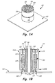
- FIG. 1A is an isometric view of a first example capacitor assembly with elements mounted perpendicular to a wiring board.
- FIG. 1B is a sectional view of the first example capacitor assembly.
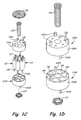
- FIG. 1C is an exploded view of the first example capacitor clamping assembly.
- FIG. 1D shows details of the first example vertical clamping assembly.
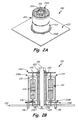
- FIG. 2A is an isometric view of a second example capacitor assembly with elements mounted perpendicular to a wiring board.
- FIG. 2B is a sectional view of the second example capacitor assembly.
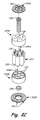
- FIG. 2C is an exploded view of the second example capacitor clamping assembly.
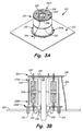
- FIG. 3A is an isometric view of a third example capacitor assembly with elements mounted perpendicular to a wiring board.
- FIG. 3B is a sectional view of the third example capacitor assembly.
- FIG. 3C is an exploded view of the third example capacitor clamping assembly.
- FIG. 4A is an isometric view of a fourth example capacitor assembly with elements mounted perpendicular to a wiring board.
- FIG. 4B is a sectional view of the fourth example capacitor assembly.
- FIG. 4C is an exploded view of the fourth example capacitor clamping assembly.
- FIG. 1A shows capacitor assembly 110, capacitor elements 112, clamping assembly 114, solder plate 116, mounting bolt 118, mounting nut 120, and printed wire board assembly (PWBA) 122.
- PWBA printed wire board assembly
- capacitor assembly 110 includes capacitor elements 112 retained vertically within clamping assembly 114.
- capacitor elements 112 are elongate and are oriented vertically, or their longitudinal axis is perpendicular to an operative mounting surface of a circuit board, here PWBA 122.
- PWBA 122 a circuit board
- capacitor elements 112 are electrically linked to the circuit(s) on PWBA 122 directly through positive leads disposed beneath capacitor assembly 110, and indirectly through capacitor clamping assembly 114.
- the clamping assembly includes a conductive path (shown shaded) to incorporate the capacitor elements to the circuit.
- PWBA 122 and its equivalents include a plurality of wiring and circuit elements for power electronics, system control, or other applications.
- PWBA wiring will vary based on each particular application and thus has been omitted for reasons of clarity from the examples provided herein.
- FIG. 1B shows capacitor assembly 110, capacitor elements 112, clamping assembly 114, solder plate 116, mounting bolt 118, mounting nut 120, printed wire board assembly (PWBA) 122, cathodes 124, anodes 126, dielectrics 128, positive leads 130, negative leads 132, capacitor insulators 133, upper clamp section 134A, lower clamp section 134B, central conductor 135, and conductive nut 137.
- PWBA printed wire board assembly
- FIG. 1B is a sectional view of assembly 110 from FIG. 1A .
- Capacitor assembly 110 is secured to PWBA 122 by mounting screw 118 and nut 120.
- Capacitor elements 112 are axial lead capacitors substantially disposed longitudinally perpendicular to PWBA 122 and respectively include cathode 124 and anode 126 with dielectric 128. Connection is made via respective cathode (negative) leads 132 and anode (positive) leads 130.
- clamping assembly 114 generally orients first positive leads 130 generally toward the mounting surface (PWBA 122) and second distal negative leads 132 away from the mounting surface. Leads 130, 132 are electrically linked to a conductive path component of clamping assembly 114, directly or indirectly joining capacitors 112 to electrical circuit(s) on PWBA 122.
- capacitor elements 112 are tantalum capacitors, available commercially from numerous vendors.
- Anode 126 is tantalum with a dielectric 128 layer of tantalum oxide.
- Solid tantalum capacitors can have a manganese oxide cathode 124. Except for leads 130, 132, cathode 124 and anode 126 are encapsulated in insulator 133 which can be an electrically insulating and thermally conductive epoxy or a urethane.
- Tantalum oxide dielectric 128 has a very high dielectric constant, allowing a very thin dielectric layer and is thus one of the highest power capacitors.
- leads 130, 132 are a copper alloy such as brass (e.g., UNS C36000, C46400, or C26000), or tellurium copper (e.g., UNS C14500).
- This combination of structural and electronic materials also aids in rejecting heat from capacitor elements 112 while maximizing electrical performance.
- Capacitor mounting assembly 114 includes solder plate 116, upper and lower clamp sections 134A, 134B, center conductive sleeve 135, and conductive nut 137.
- positive terminals 130 can be soldered or otherwise electrically connected to PWBA 122.
- Solder plate 116 is conductive and electrically joins cathodes 124 via negative leads 132.
- solder plate 116 provides an electrical current path through mounting assembly 114.
- negative charge accumulates in cathodes 124 and a positive charge accumulates in anodes 126 to maintain an electrical potential across dielectric 128.
- the conductive current path, including cathode 124 and anode 126, is shaded for illustrative purposes.
- Dielectric 128 is differentially shaded from the conductive path.
- Clamping assembly 114 (and related alternative embodiments below) reacts forces caused by vibrational and torsional stresses to ensure continued connection of capacitor assembly 110. These stresses are characteristic of operational stresses experienced by these and other high-power capacitors 112. Electrolytic tantalum capacitors are frequently used in space and military applications in power electronics to maintain operation through virtually any environment. Vertical mounting of these and other capacitors can reduce board area compared to longitudinal mounting. The mass and large profile of these and other high-power capacitors in a vertical mounting arrangement exacerbate stresses in and around the capacitor elements, which can cause the leads to prematurely wear or fracture.
- Positive leads 130 are soldered or otherwise electrically connected to PWBA 122 beneath capacitor assembly 110.
- Capacitor mounting assembly 110 includes ports or other pathways in the base (shown in FIG. 1C ) for leads 130 to extend therethrough.
- Capacitor assembly 114 allows vertical mounting of capacitor elements 112, putting the smaller form factor of the capacitor elements onto the board.
- leads 130 can be stored under the capacitor assembly rather than taking up even more board space as compared to traditional mounting of axial-lead capacitors.
- positive leads 130 are bent or folded to provide slack to accommodate thermal expansion from resistance heating. Folding also accommodates high vibration and torsional stress which may also be present depending on the operating environment.
- leads project straight from the capacitor elements and the clamping assembly includes another conductive structure to resist stresses.
- FIG. 1C shows capacitor elements 112, clamping assembly 114, solder plate 116, positive leads 130, negative leads 132, upper clamp section 134A, lower clamp section 134B, center conductive sleeve 135, recesses 136, conductive nut 137, lead pathways 138, outer pins 142A, 142B, and inner pins 144A, 144B.
- FIG. 1C is an exploded view showing capacitor elements 112 and the various components of clamping assembly 114.
- Respective upper and lower clamp sections 134A, 134B together substantially form a cylinder with recesses 136 for capacitor elements 112.
- Each recess 136 has a pathway 138 for negative and positive leads 130, 132 to protrude therethrough for connection to the conductive path.
- Positive leads 132 can be soldered or otherwise secured directly to PWBA 122 as shown in FIG. 1B .
- Negative leads 130 are soldered or secured to solder plate 116.
- solder plate 116 forms part of the conductive path linking capacitors 112 with PWBA 122.
- Clamping sections 134A, 134B can be epoxy or other electrically insulating resin to isolate the conductive path.
- clamp sections 134A, 134B can include outer pins 142A, 142B and inner pins 144A, 144B to axially stiffen assembly 110 to mitigate effects of these stresses as shown in FIG. 1D .
- FIG. 1D shows clamping assembly 114, upper clamp section 134A, lower clamp section 134B, center conductive sleeve 135, recesses 136, conductive 137, lead pathways 138, outer pins 142A, 142B, inner pins 144A, 144B, central cylinder portion 146, peripheral strut portions 148, and outer cylinder surfaces 150A, 150B.
- upper and lower clamp sections 134A, 134B each have respective outer pins 142A, 142B, projecting above and below assembly 114.
- Clamp sections 134A, 134B also each include at least one inner pin 144A, 144B projecting toward the opposing clamp section. Together these provide axial stiffness to clamping assembly 114 which minimizes torsional forces of one element relative to another.
- outer pins 142A also project through conductive solder plate 116 (shown in FIG. 1C ) and outer pins 142B project through holes in PWBA 122.
- pins 142A, 142B, 144A, 144B may be added, moved, or omitted.
- upper section 134A is an inverted instance of lower section 134B and vice versa.
- sections 134A, 134B substantially define a cylinder with central portion 146, vertical strut portions 148, and outer portions 150 linking outer parts of strut portions 148.
- Clamp sections 134A, 134B, including outer pins 142A, 142B and inner pins 144A, 144B are electrically insulating to prevent short circuits. These sections can be epoxy- or urethane-based which will also aid in heat rejection.
- the examples showing this and other embodiments depict a small gap between sections 134A, 134B, even when assembly 110 is mounted to PWBA 122 (shown in FIGS. 1A and 1B ).
- Sections 134A, 134B can alternatively fit tightly, defining a cylinder without a gap therebetween.
- capacitor assembly 110 with vertically oriented capacitor elements are shown in the remaining figures.
- FIG. 2A shows a second example embodiment with capacitor assembly 210, capacitor elements 212, clamping assembly 214, upper conductive solder plate 216A, lower mounting solder plate 216B, mounting bolt 218, mounting nut 220, and PWBA 222.
- capacitor assembly 210 includes capacitor elements 212 retained by clamping assembly 214. Capacitors 212 are secured between upper and lower solder plates 216A, 216B with axial mounting bolt 218 and nut 220.
- FIG. 2B is a sectional view of FIG. 2A showing capacitor assembly 210, capacitor elements 212, clamping assembly 214, upper conductive solder plate 216A, lower mounting solder plate 216B, mounting bolt 218, mounting nut 220, PWBA 222, cathodes 224, anodes 226, dielectrics 228, positive leads 230, negative leads 232, capacitor insulators 233, upper clamp section 234A, lower clamp section 234B, center conductive sleeve 235, insulating nut 239, and conductive pins 241.
- capacitor elements 212 each include respective cathode 224 and anode 226 with dielectric 228 disposed therebetween. These elements are surrounded by electrical insulator 233 which isolates the electrical elements from the surrounding environment. In this and the other examples, capacitor elements 212 are the same tantalum-based capacitors as described with respect to FIGS. 1A-1C .
- Clamping assembly 214 includes upper section 234A and lower portion 234B and a conductive path (shaded) with upper solder plate 216A, lower solder plate 216B, and center conductive sleeve 235.
- Upper solder plate 216A and solder plate 216B are electrically conductive to provide a conductive path through clamping assembly 214 for electrically connecting capacitors 212 to PWBA 222.
- Upper plate 216A is electrically connected to center conductive sleeve 235 to provide a conductive path to distal second (negative) leads 232 soldered thereto.
- First (positive) leads 230 project through and are soldered to lower solder plate 216B.
- the conductive path through capacitor assembly 210 is completed by connecting anodes 226 to lower solder plate 216B via positive leads 230.
- Plate 216B includes conductive pins 241 soldered to PWBA 222, which provides most or all of the electrical connection between anode 226 and circuit(s) disposed on PWBA 222.
- Positive leads 230 may or may not also be soldered to PWBA 222, depending on the electrical requirements of the particular circuit(s) for which capacitor assembly 210 is being used.
- Insulating nut 239 isolates sleeve 236 from lower solder plate 216B and positive leads 230. Insulating nut 239 threads to the end of sleeve 235, isolating it from lower solder plate 216B and positive leads 230. Together sleeve 235 and nut 239 secure capacitors 212 within clamping assemblies 234A, 234B. Positive leads 230 need not be bent to withstand torsional and vibrational stresses because plate 216B provides both a conductive path and axial stiffness through conductive pins 241.
- FIG. 2C shows capacitor elements 212, clamping assembly 214, upper solder plate 216A, lower solder plate 216B, PWBA 222, positive leads 230, negative leads 232, upper clamp section 234A, lower clamp section 234B, center conductive sleeve 235, clamp recesses 236, lead pathways 238, insulating nut 239, conductive pins 241, inner pins 244A, 244B, and upper solder plate recess 252.
- FIG. 2C is an exploded view of clamping assembly 214 with receiving sections 236 and lead pathways 238 for retaining and orienting six capacitor elements 212 perpendicular to PWBA 222. It will be appreciated that capacitor elements having different dimensions (cross-section and/or height) may result in modifying the arrangement of clamping assembly 214 with the goal of minimizing vibration and/or board area.
- Upper solder plate 216A includes annular solder plate groove 252 for plate 216A to radially expand and contract. Solder plate 216A and the elements therearound are prone to thermal expansion. Solder plate recess 252 reduces stress and breakage of negative leads 232 by providing room for expansion of various elements of the assembly.
- Lower solder plate 216B also includes a larger center aperture for receiving insulating nut 239 which electrically isolates center conductive sleeve 235. Nut 239 can be produced, for example, using a phenolic resin or other material with suitable electrically insulating and thermally conductive properties.
- FIG. 3A is a third example embodiment showing capacitor assembly 310, capacitor elements 312, clamping assembly 314, upper solder plate 316A, lower solder plate 316B, mounting screw 318, PWBA 322, cathode terminals 332, outer lead 354, and outer lead guide 356.
- Capacitor assembly 310 operates similarly to assembly 210. However, outer lead 354 is provided to conduct current and complete the conductive path in lieu of a conductive sleeve through the center of the clamping assembly. Outer lead 354 connects outer lead guide 356 on solder plate 316A with PWBA 322. Outer lead 354 can be a single wire up to negative leads 332. Capacitor assembly 310 is mounted using a downward oriented mounting bolt or screw 318, with nut 320 securing the assembly beneath PWBA 322.
- FIG. 3B is a sectional view of FIG. 3A showing capacitor assembly 310, capacitor elements 312, clamping assembly 314, upper mounting solder plate 316A, lower mounting solder plate 316B, mounting screw 318, mounting nut 320, PWBA 322, cathode 324, anode 326, dielectric 328, positive lead 330, negative lead 332, upper clamp section 334A, lower clamp section 334B, insulating ring 339, and conductive pins 341.
- FIG. 3C shows an exploded view of capacitor assembly 310 that also includes recesses 336 and lead pathways 338.
- clamping assembly 314 includes upper and lower clamp sections 334A, 334B for vertically retaining capacitor elements 312.
- upper solder plate 316A is conductive so as to electrically connect negative leads 332.
- the conductive path through capacitor assembly 310 is completed by connecting anodes 326 to lower solder plate 316B via positive leads 330.
- Plate 316B includes conductive pins 341 soldered to PWBA 322, which provides most or all of the electrical connection between the circuit(s) on PWBA 322 and anodes 326.
- Positive leads 330 may or may not also be soldered to PWBA 322, depending on the electrical requirements of the particular circuit(s) for which capacitor assembly 410 is being used.
- Lower solder plate 316B is electrically isolated from the rest of PWBA 322 by insulating ring 339.
- outer lead 354 completes the charge pathway between capacitor elements 312 and PWBA 322, avoiding the need for a center conductor in assembly 314.
- upper and lower clamping sections 334A, 334B do not include inner pins.
- clamping sections 334A, 334B can be readily adapted to include one or more inner or outer pins as seen in FIGS. 1A-1D or 2A-2C to axially stiffen capacitor assembly 310.
- Retention structures other than cylinders can be used with a conductive path and can include either open or closed sides. An example of an open-sided clamping assembly is shown in FIGS. 4A-4C .
- FIG. 4A is a fourth example embodiment of a vertical capacitor assembly.
- FIG. 4A shows capacitor assembly 410, capacitor elements 412, clamping assembly 414, upper conductive plate 416, upper plate screws 418, and PWBA 422.
- clamping assembly 414 does not fully encapsulate capacitor elements 412 with capacitors open to the environment. And instead of soldering the upper plate to the distal leads, this example shows conductive plate 416 secured directly to clamping assembly 414 by a plurality of screws 418.
- clamping assembly 414 is a single piece and leaves capacitor elements 412 open to the surrounding environment. This may be helpful, for example, when there is sufficient air flow around capacitor assembly 410 to facilitate convection cooling.
- FIG. 4B is a sectional view of FIG. 4A showing capacitor assembly 410, capacitor elements 412, upper conductive plate 416, conductive plate screws 418, board mounting screw 420, printed wire board assembly (PWBA) 422, cathode 424, anode 426, dielectric 428, positive leads 430, negative terminals 432, clamping structure 434, clamp base 460, and central strut 462.
- PWBA printed wire board assembly
- 4C is an exploded view showing capacitor assembly 410, capacitor elements 412, clamping assembly 414, upper conductive plate 416, upper plate screws 418, board mounting screw 420, positive leads 430, negative terminals 432, clamping structure 434, capacitor recesses 436, lead pathways 438, base 460, central strut 462, and peripheral struts 464.
- FIG. 4B shows one example of the conductive path through clamping assembly 414.
- FIG. 4C shows how capacitor elements 412 are retained perpendicular to PWBA 422.
- Capacitor assembly 410 is secured to PWBA 422 by center board mounting screw 420.
- Clamping assembly 414 includes clamping structure 434 having base 460 with central strut 462 and a circumferentially distributed plurality of peripheral struts 464 projecting perpendicularly therefrom. This combination of base 460 and perpendicular struts 462, 464 defines vertical recesses 436 for vertically retaining capacitor elements 412 perpendicular to PWBA 422.
- Conductive plate 416 is directly in contact with negative terminals 432. As compared to leads, terminals 432 engage more surface area at the distal ends of capacitors 412 directly with plate 416.
- the conductive path for capacitors 412 generally continues through clamping structure 434. Electrical continuity can be provided by at least an electrically conductive portion integrated as at least part of each strut 462, 464. If capacitors 412 are sufficiently isolated with insulators 433, substantially all of struts 462, 464 can form part of the conductive path. Electrical isolation can be provided by portions of base 460 and capacitor insulation 433.
- Clamping structure 434 can be soldered to PWBA 422 at various points to connect assembly 410 to the circuit. One such group of solder points can be selected directly beneath center strut 462 and peripheral struts 464. Struts 462, 464 can also be threaded for receiving conductive or non-conductive plate screws 418.
- Center strut 462 and peripheral struts 464 are arranged in generally a cylindrical orientation. This is in contrast to the outer cylindrical surface as in the previous examples showing a two-piece non-conductive clamp.
- the single piece clamp shown in FIGS. 4A-4C simplifies assembly of the capacitors and their connection to the mounting surface.
- leads 430 are shown in this example as projecting straight into PWBA 422. But as described in FIGS. 1A-1C , positive leads 430 can alternatively be bent or folded such that they retain some slack when surrounding elements of capacitor assembly 410 thermally expand and contract. As was previously noted, bending or folding leads 430 can minimize weakening or fracture from torsional and/or vibrational stresses.
Landscapes
- Engineering & Computer Science (AREA)
- Power Engineering (AREA)
- Microelectronics & Electronic Packaging (AREA)
- Manufacturing & Machinery (AREA)
- Fixed Capacitors And Capacitor Manufacturing Machines (AREA)
- Structures For Mounting Electric Components On Printed Circuit Boards (AREA)
Abstract
Description
- The invention relates generally to mounting electronic components, and more specifically to methods and apparatus for mounting capacitors.
- Capacitors mounted to circuit boards and printed wire boards are usually oriented longitudinally parallel to the board to maximize contact area and minimize the length of leads. However, in many cases, the board surface area and longtitudinal length may limit the number of capacitors that can be included, restricting the amount of capacitive storage available for certain space-restricted applications. In some applications, radial lead capacitors can be used and oriented longitudinally perpendicular to the board. However, the internal geometry of radial lead capacitors is more complex, with many high-power capacitors such as electrolytic tantalum capacitors not readily adaptable to such a design.
- Complicating the issue are high power density axial- and radial-lead capacitors, with weight, vibration, and heat that can weaken or fracture the leads. Mounting capacitors vertically (perpendicular to a mounting surface) without a support or other mounting structure actually increases these problems compared to other types of mounting. Operational torsion and heat can cause damage to the connections, the capacitor structure, and the board itself.
- A capacitor assembly comprises a plurality of capacitor elements, a clamping assembly, and a conductive path. The clamping assembly retains the plurality of capacitor elements longitudinally perpendicular to a mounting surface. The conductive path electrically connects the plurality of capacitor elements to one or more circuit elements disposed proximate the mounting surface.
- A capacitor clamping assembly comprises an upper electrically insulating section, a lower electrically insulating section, and a conductive path. A combination of the upper section and the lower section defines a cylinder having a plurality of internal recesses disposed circumferentially around the cylinder for retaining a corresponding plurality of capacitor elements longitudinally perpendicular to a mounting surface. The conductive path is provided for electrically connecting the plurality of capacitor elements to at least one electrical circuit element disposed proximate the mounting surface.
- A capacitor clamping assembly comprises a mounting base, a central strut, and a plurality of peripheral struts arranged circumferentially around the central strut. The struts project perpendicularly from the mounting base. Combination of the central strut and the plurality of peripheral struts define a plurality of recesses therebetween for retaining a corresponding plurality of capacitor elements circumferentially around the central strut in a vertical orientation and perpendicular to a mounting surface.
-
FIG. 1A is an isometric view of a first example capacitor assembly with elements mounted perpendicular to a wiring board. -
FIG. 1B is a sectional view of the first example capacitor assembly. -
FIG. 1C is an exploded view of the first example capacitor clamping assembly. -
FIG. 1D shows details of the first example vertical clamping assembly. -
FIG. 2A is an isometric view of a second example capacitor assembly with elements mounted perpendicular to a wiring board. -
FIG. 2B is a sectional view of the second example capacitor assembly. -
FIG. 2C is an exploded view of the second example capacitor clamping assembly. -
FIG. 3A is an isometric view of a third example capacitor assembly with elements mounted perpendicular to a wiring board. -
FIG. 3B is a sectional view of the third example capacitor assembly. -
FIG. 3C is an exploded view of the third example capacitor clamping assembly. -
FIG. 4A is an isometric view of a fourth example capacitor assembly with elements mounted perpendicular to a wiring board. -
FIG. 4B is a sectional view of the fourth example capacitor assembly. -
FIG. 4C is an exploded view of the fourth example capacitor clamping assembly. -
FIG. 1A showscapacitor assembly 110,capacitor elements 112,clamping assembly 114,solder plate 116,mounting bolt 118,mounting nut 120, and printed wire board assembly (PWBA) 122. - In this first example embodiment,
capacitor assembly 110 includescapacitor elements 112 retained vertically withinclamping assembly 114. In this and other example embodiments,capacitor elements 112 are elongate and are oriented vertically, or their longitudinal axis is perpendicular to an operative mounting surface of a circuit board, here PWBA 122. As will be seen in more detail inFIGS. 1B and1C ,capacitor elements 112 are electrically linked to the circuit(s) onPWBA 122 directly through positive leads disposed beneathcapacitor assembly 110, and indirectly throughcapacitor clamping assembly 114. In this and other embodiments described in subsequent figures, the clamping assembly includes a conductive path (shown shaded) to incorporate the capacitor elements to the circuit. - PWBA 122 and its equivalents include a plurality of wiring and circuit elements for power electronics, system control, or other applications. In this and all of the following examples, it will be understood that appropriate mounting and solder points and other circuitry are provided to join the capacitors to a particular circuit(s) on the PWBA. PWBA wiring will vary based on each particular application and thus has been omitted for reasons of clarity from the examples provided herein.
-
FIG. 1B showscapacitor assembly 110,capacitor elements 112,clamping assembly 114,solder plate 116,mounting bolt 118,mounting nut 120, printed wire board assembly (PWBA) 122,cathodes 124,anodes 126,dielectrics 128,positive leads 130,negative leads 132,capacitor insulators 133,upper clamp section 134A,lower clamp section 134B,central conductor 135, andconductive nut 137. -
FIG. 1B is a sectional view ofassembly 110 fromFIG. 1A .Capacitor assembly 110 is secured to PWBA 122 by mountingscrew 118 andnut 120.Capacitor elements 112 are axial lead capacitors substantially disposed longitudinally perpendicular toPWBA 122 and respectively includecathode 124 andanode 126 with dielectric 128. Connection is made via respective cathode (negative) leads 132 and anode (positive) leads 130. In this and other examples, clampingassembly 114 generally orients firstpositive leads 130 generally toward the mounting surface (PWBA 122) and second distal negative leads 132 away from the mounting surface.Leads assembly 114, directly or indirectly joiningcapacitors 112 to electrical circuit(s) onPWBA 122. - In the example embodiments described herein,
capacitor elements 112 are tantalum capacitors, available commercially from numerous vendors.Anode 126 is tantalum with a dielectric 128 layer of tantalum oxide. Solid tantalum capacitors can have amanganese oxide cathode 124. Except forleads cathode 124 andanode 126 are encapsulated ininsulator 133 which can be an electrically insulating and thermally conductive epoxy or a urethane.Tantalum oxide dielectric 128 has a very high dielectric constant, allowing a very thin dielectric layer and is thus one of the highest power capacitors. Additionally, in this example, leads 130, 132 are a copper alloy such as brass (e.g., UNS C36000, C46400, or C26000), or tellurium copper (e.g., UNS C14500). This combination of structural and electronic materials also aids in rejecting heat fromcapacitor elements 112 while maximizing electrical performance. -
Capacitor mounting assembly 114 includessolder plate 116, upper andlower clamp sections conductive sleeve 135, andconductive nut 137. To facilitate current flow,positive terminals 130 can be soldered or otherwise electrically connected toPWBA 122.Solder plate 116 is conductive and electrically joinscathodes 124 via negative leads 132. In conjunction withnut 137 and centerconductive sleeve 135 disposed through the center ofclamp sections solder plate 116 provides an electrical current path through mountingassembly 114. As also seen inFIG. 1B , negative charge accumulates incathodes 124 and a positive charge accumulates inanodes 126 to maintain an electrical potential acrossdielectric 128. The conductive current path, includingcathode 124 andanode 126, is shaded for illustrative purposes.Dielectric 128 is differentially shaded from the conductive path. - Clamping assembly 114 (and related alternative embodiments below) reacts forces caused by vibrational and torsional stresses to ensure continued connection of
capacitor assembly 110. These stresses are characteristic of operational stresses experienced by these and other high-power capacitors 112. Electrolytic tantalum capacitors are frequently used in space and military applications in power electronics to maintain operation through virtually any environment. Vertical mounting of these and other capacitors can reduce board area compared to longitudinal mounting. The mass and large profile of these and other high-power capacitors in a vertical mounting arrangement exacerbate stresses in and around the capacitor elements, which can cause the leads to prematurely wear or fracture. - Positive leads 130 are soldered or otherwise electrically connected to
PWBA 122 beneathcapacitor assembly 110.Capacitor mounting assembly 110 includes ports or other pathways in the base (shown inFIG. 1C ) forleads 130 to extend therethrough.Capacitor assembly 114 allows vertical mounting ofcapacitor elements 112, putting the smaller form factor of the capacitor elements onto the board. In addition, leads 130 can be stored under the capacitor assembly rather than taking up even more board space as compared to traditional mounting of axial-lead capacitors. In this example,positive leads 130 are bent or folded to provide slack to accommodate thermal expansion from resistance heating. Folding also accommodates high vibration and torsional stress which may also be present depending on the operating environment. Alternatively, in other embodiments, leads project straight from the capacitor elements and the clamping assembly includes another conductive structure to resist stresses. -
FIG. 1C showscapacitor elements 112, clampingassembly 114,solder plate 116, positive leads 130, negative leads 132,upper clamp section 134A,lower clamp section 134B, centerconductive sleeve 135, recesses 136,conductive nut 137,lead pathways 138,outer pins inner pins -
FIG. 1C is an exploded view showingcapacitor elements 112 and the various components of clampingassembly 114. Respective upper andlower clamp sections recesses 136 forcapacitor elements 112. Eachrecess 136 has apathway 138 for negative andpositive leads PWBA 122 as shown inFIG. 1B . Negative leads 130 are soldered or secured tosolder plate 116. In conjunction with centerconductive sleeve 135 andnut 137,solder plate 116 forms part of the conductivepath linking capacitors 112 withPWBA 122. Clampingsections - As described with respect to
FIG. 1B , vertical mounting ofcapacitor elements 112 saves a substantial amount of mounting area onPWBA 122, but also can increase vibration and torsional forces that could damage or fracture leads 130. Thus, in addition to bending or folding leads 130,clamp sections outer pins inner pins assembly 110 to mitigate effects of these stresses as shown inFIG. 1D . -
FIG. 1D shows clampingassembly 114,upper clamp section 134A,lower clamp section 134B, centerconductive sleeve 135, recesses 136, conductive 137,lead pathways 138,outer pins inner pins central cylinder portion 146,peripheral strut portions 148, and outer cylinder surfaces 150A, 150B. - In addition to
recesses 136 andlead pathways 138 for capacitor elements 112 (shown inFIGS. 1A-1C ), upper andlower clamp sections outer pins assembly 114.Clamp sections inner pin assembly 114 which minimizes torsional forces of one element relative to another. As seen inFIG. 1C ,outer pins 142A also project through conductive solder plate 116 (shown inFIG. 1C ) andouter pins 142B project through holes inPWBA 122. In combination withinner pins FIGS. 1B and1C ). In alternative embodiments, depending on the anticipated or actual operational forces, any or all ofpins - In this case,
upper section 134A is an inverted instance oflower section 134B and vice versa. Together,sections central portion 146,vertical strut portions 148, and outer portions 150 linking outer parts ofstrut portions 148.Clamp sections outer pins inner pins sections assembly 110 is mounted to PWBA 122 (shown inFIGS. 1A and 1B ). This is primarily for illustrative purposes and any gap is exaggerated to better show the twoseparate sections capacitor elements 112.Sections capacitor assembly 110 with vertically oriented capacitor elements are shown in the remaining figures. -
FIG. 2A shows a second example embodiment withcapacitor assembly 210,capacitor elements 212, clampingassembly 214, upperconductive solder plate 216A, lower mountingsolder plate 216B, mountingbolt 218, mountingnut 220, andPWBA 222. - In this second example embodiment,
capacitor assembly 210 includescapacitor elements 212 retained by clampingassembly 214.Capacitors 212 are secured between upper andlower solder plates axial mounting bolt 218 andnut 220. -
FIG. 2B is a sectional view ofFIG. 2A showingcapacitor assembly 210,capacitor elements 212, clampingassembly 214, upperconductive solder plate 216A, lower mountingsolder plate 216B, mountingbolt 218, mountingnut 220,PWBA 222,cathodes 224,anodes 226,dielectrics 228, positive leads 230, negative leads 232,capacitor insulators 233,upper clamp section 234A,lower clamp section 234B, centerconductive sleeve 235, insulatingnut 239, andconductive pins 241. - Like
FIGS. 1A-1C ,capacitor elements 212 each includerespective cathode 224 andanode 226 with dielectric 228 disposed therebetween. These elements are surrounded byelectrical insulator 233 which isolates the electrical elements from the surrounding environment. In this and the other examples,capacitor elements 212 are the same tantalum-based capacitors as described with respect toFIGS. 1A-1C . - Clamping
assembly 214 includesupper section 234A andlower portion 234B and a conductive path (shaded) withupper solder plate 216A,lower solder plate 216B, and centerconductive sleeve 235.Upper solder plate 216A andsolder plate 216B are electrically conductive to provide a conductive path through clampingassembly 214 for electrically connectingcapacitors 212 toPWBA 222.Upper plate 216A is electrically connected to centerconductive sleeve 235 to provide a conductive path to distal second (negative) leads 232 soldered thereto. First (positive) leads 230 project through and are soldered tolower solder plate 216B. The conductive path throughcapacitor assembly 210 is completed by connectinganodes 226 tolower solder plate 216B via positive leads 230.Plate 216B includesconductive pins 241 soldered toPWBA 222, which provides most or all of the electrical connection betweenanode 226 and circuit(s) disposed onPWBA 222. Positive leads 230 may or may not also be soldered toPWBA 222, depending on the electrical requirements of the particular circuit(s) for whichcapacitor assembly 210 is being used. - Insulating
nut 239 isolatessleeve 236 fromlower solder plate 216B and positive leads 230. Insulatingnut 239 threads to the end ofsleeve 235, isolating it fromlower solder plate 216B and positive leads 230. Togethersleeve 235 andnut 239secure capacitors 212 within clampingassemblies plate 216B provides both a conductive path and axial stiffness throughconductive pins 241. -
FIG. 2C showscapacitor elements 212, clampingassembly 214,upper solder plate 216A,lower solder plate 216B,PWBA 222, positive leads 230, negative leads 232,upper clamp section 234A,lower clamp section 234B, centerconductive sleeve 235, clamp recesses 236,lead pathways 238, insulatingnut 239,conductive pins 241,inner pins solder plate recess 252. -
FIG. 2C is an exploded view of clampingassembly 214 with receivingsections 236 andlead pathways 238 for retaining and orienting sixcapacitor elements 212 perpendicular toPWBA 222. It will be appreciated that capacitor elements having different dimensions (cross-section and/or height) may result in modifying the arrangement of clampingassembly 214 with the goal of minimizing vibration and/or board area. -
Upper solder plate 216A includes annularsolder plate groove 252 forplate 216A to radially expand and contract.Solder plate 216A and the elements therearound are prone to thermal expansion.Solder plate recess 252 reduces stress and breakage ofnegative leads 232 by providing room for expansion of various elements of the assembly.Lower solder plate 216B also includes a larger center aperture for receiving insulatingnut 239 which electrically isolates centerconductive sleeve 235.Nut 239 can be produced, for example, using a phenolic resin or other material with suitable electrically insulating and thermally conductive properties. -
FIG. 3A is a third example embodiment showingcapacitor assembly 310,capacitor elements 312, clampingassembly 314,upper solder plate 316A,lower solder plate 316B, mountingscrew 318,PWBA 322,cathode terminals 332,outer lead 354, and outerlead guide 356. -
Capacitor assembly 310 operates similarly toassembly 210. However,outer lead 354 is provided to conduct current and complete the conductive path in lieu of a conductive sleeve through the center of the clamping assembly.Outer lead 354 connects outerlead guide 356 onsolder plate 316A withPWBA 322.Outer lead 354 can be a single wire up to negative leads 332.Capacitor assembly 310 is mounted using a downward oriented mounting bolt or screw 318, withnut 320 securing the assembly beneathPWBA 322. -
FIG. 3B is a sectional view ofFIG. 3A showingcapacitor assembly 310,capacitor elements 312, clampingassembly 314, upper mountingsolder plate 316A, lower mountingsolder plate 316B, mountingscrew 318, mountingnut 320,PWBA 322,cathode 324,anode 326, dielectric 328,positive lead 330,negative lead 332,upper clamp section 334A,lower clamp section 334B, insulatingring 339, andconductive pins 341.FIG. 3C shows an exploded view ofcapacitor assembly 310 that also includesrecesses 336 andlead pathways 338. - Like other embodiments described above, clamping
assembly 314 includes upper andlower clamp sections capacitor elements 312. Similarly,upper solder plate 316A is conductive so as to electrically connect negative leads 332. The conductive path throughcapacitor assembly 310 is completed by connectinganodes 326 tolower solder plate 316B via positive leads 330.Plate 316B includesconductive pins 341 soldered toPWBA 322, which provides most or all of the electrical connection between the circuit(s) onPWBA 322 andanodes 326. Positive leads 330 may or may not also be soldered toPWBA 322, depending on the electrical requirements of the particular circuit(s) for whichcapacitor assembly 410 is being used.Lower solder plate 316B is electrically isolated from the rest ofPWBA 322 by insulatingring 339. - As noted with respect to
FIG. 3A ,outer lead 354 completes the charge pathway betweencapacitor elements 312 andPWBA 322, avoiding the need for a center conductor inassembly 314. It should also be noted that, unlike the previous examples, upper andlower clamping sections sections FIGS. 1A-1D or2A-2C to axially stiffencapacitor assembly 310. Retention structures other than cylinders can be used with a conductive path and can include either open or closed sides. An example of an open-sided clamping assembly is shown inFIGS. 4A-4C . -
FIG. 4A is a fourth example embodiment of a vertical capacitor assembly.FIG. 4A showscapacitor assembly 410,capacitor elements 412, clampingassembly 414, upperconductive plate 416, upper plate screws 418, andPWBA 422. - Unlike the previous examples, clamping
assembly 414 does not fully encapsulatecapacitor elements 412 with capacitors open to the environment. And instead of soldering the upper plate to the distal leads, this example showsconductive plate 416 secured directly to clampingassembly 414 by a plurality ofscrews 418. Thus, in contrast to previous examples, clampingassembly 414 is a single piece and leavescapacitor elements 412 open to the surrounding environment. This may be helpful, for example, when there is sufficient air flow aroundcapacitor assembly 410 to facilitate convection cooling. -
FIG. 4B is a sectional view ofFIG. 4A showingcapacitor assembly 410,capacitor elements 412, upperconductive plate 416, conductive plate screws 418,board mounting screw 420, printed wire board assembly (PWBA) 422,cathode 424,anode 426, dielectric 428, positive leads 430,negative terminals 432, clampingstructure 434,clamp base 460, andcentral strut 462.FIG. 4C is an exploded view showingcapacitor assembly 410,capacitor elements 412, clampingassembly 414, upperconductive plate 416, upper plate screws 418,board mounting screw 420, positive leads 430,negative terminals 432, clampingstructure 434, capacitor recesses 436, lead pathways 438,base 460,central strut 462, and peripheral struts 464. -
FIG. 4B shows one example of the conductive path through clampingassembly 414.FIG. 4C shows howcapacitor elements 412 are retained perpendicular toPWBA 422.Capacitor assembly 410 is secured toPWBA 422 by centerboard mounting screw 420. Clampingassembly 414 includes clampingstructure 434 havingbase 460 withcentral strut 462 and a circumferentially distributed plurality ofperipheral struts 464 projecting perpendicularly therefrom. This combination ofbase 460 andperpendicular struts capacitor elements 412 perpendicular toPWBA 422. -
Conductive plate 416 is directly in contact withnegative terminals 432. As compared to leads,terminals 432 engage more surface area at the distal ends ofcapacitors 412 directly withplate 416. The conductive path forcapacitors 412 generally continues through clampingstructure 434. Electrical continuity can be provided by at least an electrically conductive portion integrated as at least part of eachstrut capacitors 412 are sufficiently isolated withinsulators 433, substantially all ofstruts base 460 andcapacitor insulation 433. Clampingstructure 434 can be soldered toPWBA 422 at various points to connectassembly 410 to the circuit. One such group of solder points can be selected directly beneathcenter strut 462 andperipheral struts 464.Struts -
Center strut 462 andperipheral struts 464 are arranged in generally a cylindrical orientation. This is in contrast to the outer cylindrical surface as in the previous examples showing a two-piece non-conductive clamp. The single piece clamp shown inFIGS. 4A-4C simplifies assembly of the capacitors and their connection to the mounting surface. - Additionally, leads 430 are shown in this example as projecting straight into
PWBA 422. But as described inFIGS. 1A-1C ,positive leads 430 can alternatively be bent or folded such that they retain some slack when surrounding elements ofcapacitor assembly 410 thermally expand and contract. As was previously noted, bending or folding leads 430 can minimize weakening or fracture from torsional and/or vibrational stresses. - The following clauses set out features of the invention which may not presently be claimed in this application but which may form the basis for future amendment or a divisional application.
- 1. A capacitor assembly comprising:
- a plurality of capacitor elements;
- a clamping assembly for retaining the plurality of capacitor elements longitudinally perpendicular to a mounting surface; and
- a conductive path for electrically connecting the plurality of capacitor elements to at least one circuit element disposed proximate the adjacent mounting surface.
- 2. The capacitor assembly of clause 1, wherein the plurality of capacitor elements is a plurality of axial-lead capacitor elements retained by the clamping assembly such that a first lead projects from the capacitor assembly generally toward the mounting surface.
- 3. The capacitor assembly of clause 2, wherein the plurality of first leads are bent to accommodate thermal expansion of the capacitor assembly.
- 4. The capacitor assembly of clause 1, further comprising a lower solder plate for electrically connecting the respective first lead of each of the plurality of capacitor elements.
- 5. The capacitor assembly of clause 1, further comprising an upper solder plate for electrically connecting a respective second lead of each of the plurality of capacitor elements.
- 6. The capacitor assembly of clause 5, wherein the upper solder plate includes a radial recessed portion proximate a center of the plate.
- 7. The capacitor assembly of clause 1, wherein the adjacent mounting surface is a surface of a printed wire board assembly (PWBA).
- 8. The capacitor assembly of clause 1, wherein an anode section of the plurality of capacitor elements comprises tantalum metal.
- 9. The capacitor assembly of clause 8, wherein a dielectric section of the plurality of capacitor elements comprises tantalum oxide formed on the tantalum anode.
- 10. The capacitor assembly of clause 1, wherein the clamping assembly comprises an upper section and a lower section, the upper and lower sections together defining a cylinder with a plurality of recesses disposed circumferentially around an interior of the clamping assembly.
- 11. The capacitor assembly of clause 10, wherein the clamping assembly includes a central conductive path
- 12. The capacitor assembly of clause 1, wherein the clamping assembly comprises a base with a central strut and a plurality of peripheral struts projecting perpendicularly therefrom.
- 13. The capacitor assembly of clause 12, wherein the conductive path is integrated with the clamping assembly.
- 14. A capacitor clamping assembly comprising:
- an upper electrically insulating section;
- a lower electrically insulating section, a combination of the upper section and the lower section defining a cylinder having a plurality of internal recesses disposed circumferentially around the cylinder for retaining a corresponding plurality of capacitor elements longitudinally perpendicular to a mounting surface; and
- a conductive path for electrically connecting the plurality of capacitor elements to at least one electrical circuit element disposed proximate the mounting surface.
- 15. The capacitor clamping assembly of clause 14, wherein one or more mounting pins project axially from at least one of the upper section and the lower section, the one or more mounting pins providing axial stiffness to the clamping assembly.
- 16. The capacitor clamping assembly of clause 14, further comprising an electrically conductive upper solder plate.
- 17. The capacitor clamping assembly of clause 16, further comprising an electrically conductive lower solder plate.
- 18. The capacitor clamping assembly of clause 17, wherein the lower solder plate includes a plurality of electrically conductive mounting pins.
- 19. The capacitor clamping assembly of clause 14, further comprising a central conductive sleeve disposed through the upper and lower clamping assembly and defining a portion of the conductive path.
- 20. A capacitor clamping assembly comprising:
- a mounting base;
- a central strut projecting perpendicularly from the mounting base; and
- a plurality of peripheral struts projecting perpendicularly from the base and arranged circumferentially around the central strut, with a combination of the central portion and the plurality of vertical struts defining a plurality of recesses therebetween for retaining a corresponding plurality of capacitor elements circumferentially around the central strut in a vertical orientation and perpendicular to a mounting surface.
- 21. The capacitor clamping assembly of clause 20, wherein at least a portion of each of the central strut and the peripheral struts are electrically conductive.
- 22. The capacitor clamping assembly of clause 21, further comprising an electrically conductive upper plate removably securable to at least one of the struts, wherein the upper plate in conjunction with the electrically conductive portions of the conductive strut and peripheral struts define a conductive path for electrically connecting the plurality of capacitor elements to at least one electrical circuit element disposed proximate the mounting surface.
- 23. The capacitor clamping assembly of clause 20, wherein the central strut includes an electrically conductive section internally traversing the central portion between a top surface of the central portion and the base.
- 24. The capacitor clamping assembly of clause 20, wherein the plurality of peripheral struts each include an electrically conductive section internally traversing each peripheral strut between a top surface of the peripheral strut and the base.
- While the invention has been described with reference to several exemplary embodiments, it will be understood by those skilled in the art that various changes may be made and equivalents may be substituted for elements thereof without departing from the scope of the invention. In addition, many modifications may be made to adapt a particular situation or material to the teachings of the invention without departing from the scope thereof. Therefore, it is intended that the invention not be limited to the particular embodiments disclosed, but that the invention will include all embodiments falling within the scope of the appended claims.
Claims (15)
- A capacitor assembly comprising:a plurality of capacitor elements;a clamping assembly for retaining the plurality of capacitor elements longitudinally perpendicular to a mounting surface; anda conductive path for electrically connecting the plurality of capacitor elements to at least one circuit element disposed proximate the adjacent mounting surface.
- The capacitor assembly of claim 1, wherein the plurality of capacitor elements is a plurality of axial-lead capacitor elements retained by the clamping assembly such that a first lead projects from the capacitor assembly generally toward the mounting surface.
- The capacitor assembly of claim 2, wherein the plurality of first leads are bent to accommodate thermal expansion of the capacitor assembly.
- The capacitor assembly of claim 1, 2 or 3 further comprising a lower solder plate for electrically connecting the respective first lead of each of the plurality of capacitor elements; preferably
wherein the lower solder plate includes a plurality of electrically conductive mounting pins. - The capacitor assembly of any preceding claim, further comprising an upper solder plate for electrically connecting a respective second lead of each of the plurality of capacitor elements; preferably
wherein the upper solder plate includes a radial recessed portion proximate a center of the plate. - The capacitor assembly of any preceding claim, wherein the clamping assembly comprises an upper section and a lower section, the upper and lower sections together defining a cylinder with a plurality of recesses disposed circumferentially around an interior of the clamping assembly; preferably
wherein the clamping assembly includes a central conductive path. - The capacitor assembly of claim 1 or 2, wherein the clamping assembly comprises a base with a central strut and a plurality of peripheral struts projecting perpendicularly therefrom; preferably
wherein the conductive path is integrated with the clamping assembly. - The capacitor assembly of any preceding claim, wherein the adjacent mounting surface is a surface of a printed wire board assembly (PWBA).
- The capacitor assembly of any preceding claim, wherein an anode section of the plurality of capacitor elements comprises tantalum metal; preferably
wherein a dielectric section of the plurality of capacitor elements comprises tantalum oxide formed on the tantalum anode. - A capacitor clamping assembly for the capacitor assembly of any of claims 1 to 6, comprising:an upper electrically insulating section;a lower electrically insulating section, a combination of the upper section and the lower section defining a cylinder having a plurality of internal recesses disposed circumferentially around the cylinder for retaining a corresponding plurality of capacitor elements longitudinally perpendicular to a mounting surface; anda conductive path for electrically connecting the plurality of capacitor elements to at least one electrical circuit element disposed proximate the mounting surface.
- The capacitor clamping assembly of claim 10, wherein one or more mounting pins project axially from at least one of the upper section and the lower section, the one or more mounting pins providing axial stiffness to the clamping assembly.
- The capacitor clamping assembly of claim 10 or 11, further comprising a central conductive sleeve disposed through the upper and lower clamping assembly and defining a portion of the conductive path.
- A capacitor clamping assembly for the assembly of claim 1, 2 or 7, comprising:a mounting base for mounting to a mounting surface;a central strut projecting perpendicularly from the mounting base; anda plurality of peripheral struts projecting perpendicularly from the base and arranged in positions circumferentially around the central strut, with a combination of the central strut and the plurality of vertical struts defining a plurality of recesses therebetween for retaining a corresponding plurality of capacitor elements in positions circumferentially around the central strut oriented alongside the struts and perpendicular to the mounting surface.
- The capacitor clamping assembly of claim 13, wherein at least a portion of each of the central strut and the peripheral struts are electrically conductive; preferably
further comprising an electrically conductive upper plate removably securable to at least one of the struts, wherein the upper plate in conjunction with the electrically conductive portions of the conductive strut and peripheral struts define a conductive path for electrically connecting the plurality of capacitor elements to at least one electrical circuit element disposed proximate the mounting surface. - The capacitor clamping assembly of claim 13 or 14, wherein the central strut includes an electrically conductive section internally traversing the central portion between a top surface of the central portion and the base; and/or
wherein the plurality of peripheral struts each include an electrically conductive section internally traversing each peripheral strut between a top surface of the peripheral strut and the base.
Applications Claiming Priority (1)
| Application Number | Priority Date | Filing Date | Title |
|---|---|---|---|
| US13/284,175 US8837166B2 (en) | 2011-10-28 | 2011-10-28 | Vertically mounted capacitor assembly |
Publications (2)
| Publication Number | Publication Date |
|---|---|
| EP2587504A1 true EP2587504A1 (en) | 2013-05-01 |
| EP2587504B1 EP2587504B1 (en) | 2023-11-29 |
Family
ID=47263079
Family Applications (1)
| Application Number | Title | Priority Date | Filing Date |
|---|---|---|---|
| EP12190460.1A Active EP2587504B1 (en) | 2011-10-28 | 2012-10-29 | Vertically mounted capacitor assembly |
Country Status (3)
| Country | Link |
|---|---|
| US (2) | US8837166B2 (en) |
| EP (1) | EP2587504B1 (en) |
| JP (2) | JP5670984B2 (en) |
Cited By (2)
| Publication number | Priority date | Publication date | Assignee | Title |
|---|---|---|---|---|
| WO2015104114A1 (en) * | 2014-01-10 | 2015-07-16 | Siemens Aktiengesellschaft | Capacitor assembly |
| CN108885945A (en) * | 2016-03-16 | 2018-11-23 | Ls美创有限公司 | Energy storage module connection structural bodies |
Families Citing this family (6)
| Publication number | Priority date | Publication date | Assignee | Title |
|---|---|---|---|---|
| US9552977B2 (en) * | 2012-12-10 | 2017-01-24 | Intel Corporation | Landside stiffening capacitors to enable ultrathin and other low-Z products |
| US9585255B2 (en) | 2015-03-11 | 2017-02-28 | Raytheon Company | Component support for dense circuit board |
| CN108356466A (en) * | 2018-03-30 | 2018-08-03 | 苏州宏泉高压电容器有限公司 | Capacitor welder |
| EP4148752A1 (en) * | 2021-09-10 | 2023-03-15 | ABB Schweiz AG | Capacitor assembly |
| US12606035B2 (en) * | 2022-12-06 | 2026-04-21 | Volkswagen Aktiengesellschaft | Devices, systems, and methods for wireless vehicle charging |
| JP7872221B2 (en) * | 2022-12-07 | 2026-06-09 | ルビコン株式会社 | Capacitance device |
Citations (5)
| Publication number | Priority date | Publication date | Assignee | Title |
|---|---|---|---|---|
| GB313600A (en) * | 1928-06-16 | 1930-02-06 | Haefely & Cie Ag Emil | Improvements in electrical condensers |
| US3456157A (en) * | 1967-06-12 | 1969-07-15 | Mallory & Co Inc P R | Electronic assembly |
| US20040251558A1 (en) * | 2003-06-16 | 2004-12-16 | Nec Tokin Corporation | Chip-type solid electrolytic capacitor and method of producing the same |
| EP1589547A1 (en) * | 2003-09-18 | 2005-10-26 | Matsushita Electric Industrial Co., Ltd. | Capacitor unit |
| US20090096418A1 (en) * | 2007-10-12 | 2009-04-16 | Roger Abadia | Electrical energy storage device, in particular for equipping a motor vehicle |
Family Cites Families (38)
| Publication number | Priority date | Publication date | Assignee | Title |
|---|---|---|---|---|
| JPS5162049U (en) * | 1974-11-09 | 1976-05-15 | ||
| US4179725A (en) | 1977-09-19 | 1979-12-18 | Union Carbide Corporation | Conformally epoxy coated electrolyte capacitor having axial leads |
| JPS5463259U (en) * | 1977-10-13 | 1979-05-04 | ||
| JPS6028447B2 (en) * | 1978-06-22 | 1985-07-04 | 太陽誘電株式会社 | Composite LC filter and its manufacturing method |
| JPS55141978U (en) * | 1979-03-30 | 1980-10-11 | ||
| JPS55141978A (en) | 1979-04-20 | 1980-11-06 | Nisshin Haiboruteeji Kk | Dc high-voltage generating device |
| US4340818A (en) | 1980-05-14 | 1982-07-20 | The Board Of Trustees Of The University Of Alabama | Scanning grid apparatus for suppressing scatter in radiographic imaging |
| JPS6012284Y2 (en) * | 1980-09-19 | 1985-04-20 | 日本ケミコン株式会社 | Electrolytic capacitor |
| FR2492577A1 (en) | 1980-10-16 | 1982-04-23 | Alsthom Atlantique | Insulating enclosures for three phase electrical power condensers - involving a plastic box with laminate board partitions to contain potting resins without a dedicated mould |
| JPS58127631U (en) * | 1982-02-19 | 1983-08-30 | 松下電器産業株式会社 | three phase capacitor |
| DE8620714U1 (en) * | 1986-08-01 | 1986-11-20 | C. & E. Fein GmbH & Co KG, 70176 Stuttgart | Sterilizable battery |
| JPS6349222U (en) * | 1986-09-17 | 1988-04-04 | ||
| JPH0511660Y2 (en) * | 1988-06-01 | 1993-03-23 | ||
| JPH0620027B2 (en) | 1989-07-26 | 1994-03-16 | 日本ケミコン株式会社 | Electrolytic capacitor mounting structure |
| JPH0420223U (en) * | 1990-06-12 | 1992-02-20 | ||
| JP2508525Y2 (en) * | 1990-06-19 | 1996-08-28 | 株式会社東芝 | Pressure contact type capacitor |
| JPH0451101U (en) * | 1990-09-03 | 1992-04-30 | ||
| JPH09120812A (en) * | 1995-10-27 | 1997-05-06 | Fuji Elelctrochem Co Ltd | Collective battery |
| JPH09190862A (en) * | 1996-01-08 | 1997-07-22 | Toshiba Corp | Socket with detachable function for chip type electronic parts |
| JPH10106898A (en) * | 1996-09-27 | 1998-04-24 | Rohm Co Ltd | Structure of capacitor element used for solid electrolytic capacitor and method for solidifying chip body in capacitor element |
| US5895293A (en) * | 1997-04-23 | 1999-04-20 | The Whitaker Corporation | Filtered terminal block assembly |
| JP3056645U (en) * | 1998-08-10 | 1999-02-26 | 邱紀電子股▲ふん▼有限公司 | Modularized electronic component fixing device |
| JP2001185240A (en) * | 1999-12-28 | 2001-07-06 | Honda Motor Co Ltd | Energy storage device |
| JP3649983B2 (en) * | 2000-01-31 | 2005-05-18 | 三洋電機株式会社 | Pack battery |
| JP3586166B2 (en) | 2000-03-31 | 2004-11-10 | Fdk株式会社 | Collective battery |
| JP2002190654A (en) * | 2000-12-21 | 2002-07-05 | Kondo Denki:Kk | Holder for electronic components mounted on board |
| JP3914865B2 (en) * | 2002-12-06 | 2007-05-16 | 松下電器産業株式会社 | Metallized film capacitors |
| JP2005199739A (en) | 2004-01-13 | 2005-07-28 | Matsushita Electric Ind Co Ltd | Voltage-dependent on-vehicle equipment and vehicles equipped with the same |
| JP2006318676A (en) | 2005-05-10 | 2006-11-24 | Sanyo Electric Co Ltd | Battery module |
| JP2007242860A (en) * | 2006-03-08 | 2007-09-20 | Toyota Motor Corp | Capacitor module |
| JP2008204989A (en) * | 2007-02-16 | 2008-09-04 | Matsushita Electric Ind Co Ltd | Capacitor unit and manufacturing method therefor |
| JP2008204981A (en) | 2007-02-16 | 2008-09-04 | Matsushita Electric Ind Co Ltd | Capacitor unit |
| US7791901B2 (en) * | 2007-05-24 | 2010-09-07 | Delphi Technologies, Inc. | Stand-off mounting apparatus for discrete electrical components |
| JP2010165597A (en) * | 2009-01-16 | 2010-07-29 | Toyota Motor Corp | Energy storage device |
| WO2011040352A1 (en) * | 2009-09-30 | 2011-04-07 | 三洋電機株式会社 | Electrolytic capacitor |
| DE102009046403B4 (en) * | 2009-11-04 | 2015-05-28 | Semikron Elektronik Gmbh & Co. Kg | Power semiconductor module in pressure contact technology |
| JP5636248B2 (en) | 2010-10-06 | 2014-12-03 | 株式会社ぐるなび | Sales support system |
| US8570767B2 (en) * | 2011-03-21 | 2013-10-29 | Deere & Company | Capacitor assembly |
-
2011
- 2011-10-28 US US13/284,175 patent/US8837166B2/en active Active
-
2012
- 2012-10-26 JP JP2012236228A patent/JP5670984B2/en active Active
- 2012-10-29 EP EP12190460.1A patent/EP2587504B1/en active Active
-
2014
- 2014-09-15 US US14/487,014 patent/US9355782B2/en active Active
- 2014-12-18 JP JP2014255736A patent/JP6109807B2/en active Active
Patent Citations (5)
| Publication number | Priority date | Publication date | Assignee | Title |
|---|---|---|---|---|
| GB313600A (en) * | 1928-06-16 | 1930-02-06 | Haefely & Cie Ag Emil | Improvements in electrical condensers |
| US3456157A (en) * | 1967-06-12 | 1969-07-15 | Mallory & Co Inc P R | Electronic assembly |
| US20040251558A1 (en) * | 2003-06-16 | 2004-12-16 | Nec Tokin Corporation | Chip-type solid electrolytic capacitor and method of producing the same |
| EP1589547A1 (en) * | 2003-09-18 | 2005-10-26 | Matsushita Electric Industrial Co., Ltd. | Capacitor unit |
| US20090096418A1 (en) * | 2007-10-12 | 2009-04-16 | Roger Abadia | Electrical energy storage device, in particular for equipping a motor vehicle |
Cited By (3)
| Publication number | Priority date | Publication date | Assignee | Title |
|---|---|---|---|---|
| WO2015104114A1 (en) * | 2014-01-10 | 2015-07-16 | Siemens Aktiengesellschaft | Capacitor assembly |
| CN108885945A (en) * | 2016-03-16 | 2018-11-23 | Ls美创有限公司 | Energy storage module connection structural bodies |
| EP3432331A4 (en) * | 2016-03-16 | 2019-11-20 | LS Mtron Ltd. | CONNECTION STRUCTURE FOR ENERGY STORAGE MODULE |
Also Published As
| Publication number | Publication date |
|---|---|
| JP2015079989A (en) | 2015-04-23 |
| US8837166B2 (en) | 2014-09-16 |
| JP5670984B2 (en) | 2015-02-18 |
| US20130107492A1 (en) | 2013-05-02 |
| JP2013098558A (en) | 2013-05-20 |
| JP6109807B2 (en) | 2017-04-05 |
| US20150003031A1 (en) | 2015-01-01 |
| EP2587504B1 (en) | 2023-11-29 |
| US9355782B2 (en) | 2016-05-31 |
Similar Documents
| Publication | Publication Date | Title |
|---|---|---|
| US9355782B2 (en) | Vertically mounted capacitor assembly | |
| JP6115791B2 (en) | Electronic device including capacitor in circuit board holder, and method of manufacturing electronic device | |
| US8351216B2 (en) | Layered structure connection and assembly | |
| JP6347768B2 (en) | Capacitor structure | |
| US20100018753A1 (en) | High voltage device, high voltage bushing and method of assembling said device | |
| CN114342024B (en) | Capacitor and method for manufacturing the same, and method for mounting the capacitor | |
| AU2023204342B2 (en) | Semiconductor device, printed circuit board (PCB), and method of interfacing control pin (gate pin) of a power semiconductor device (MOSFET) to a printed circuit board (PCB) in a battery management system (BMS) | |
| CN108885945B (en) | Connection structure for energy storage module | |
| US20240244796A1 (en) | Circuit device | |
| CN112673436A (en) | Electrical bushing with anti-rotation mounting flange and method of mounting an electrical bushing | |
| EP1430493B1 (en) | Multiple terminal smt-bga-style wound capacitor | |
| JP4803749B2 (en) | Metallized film capacitors | |
| KR102876625B1 (en) | High frequency and current capacitor assembly | |
| EP2117014B1 (en) | High voltage bushing contact, high voltage bushing comprising such contact and high voltage device comprising bushing with such contact | |
| US20240407077A1 (en) | Printed circuit board and method of manufacturing the same | |
| US12080634B2 (en) | Semiconductor device, printed circuit board (PCB), and method of interfacing control pin (gate pin) of a power semiconductor device (MOSFET) to a printed circuit board (PCB) | |
| JPH041718Y2 (en) | ||
| US10297935B2 (en) | Power supply and circuit board output structure thereof | |
| EP4066317A1 (en) | Semiconductor device, printed circuit board (pcb), and method of interfacing control pin (gate pin) of a power semiconductor device (mosfet) to a printed circuit board (pcb) in a battery management system (bms) | |
| US20060145360A1 (en) | Wound capacitor | |
| JP2007165546A (en) | Film capacitor | |
| JPH0623238U (en) | High voltage capacitor and magnetron | |
| CN115440501A (en) | A voltage equalizing insulating cylinder and a voltage equalizing capacitor string thereof | |
| JPH10116751A (en) | Capacitor unit | |
| KR20160020330A (en) | Capacitor module apparatus and method for manufacturing the same |
Legal Events
| Date | Code | Title | Description |
|---|---|---|---|
| PUAI | Public reference made under article 153(3) epc to a published international application that has entered the european phase |
Free format text: ORIGINAL CODE: 0009012 |
|
| AK | Designated contracting states |
Kind code of ref document: A1 Designated state(s): AL AT BE BG CH CY CZ DE DK EE ES FI FR GB GR HR HU IE IS IT LI LT LU LV MC MK MT NL NO PL PT RO RS SE SI SK SM TR |
|
| AX | Request for extension of the european patent |
Extension state: BA ME |
|
| 17P | Request for examination filed |
Effective date: 20131101 |
|
| RBV | Designated contracting states (corrected) |
Designated state(s): AL AT BE BG CH CY CZ DE DK EE ES FI FR GB GR HR HU IE IS IT LI LT LU LV MC MK MT NL NO PL PT RO RS SE SI SK SM TR |
|
| STAA | Information on the status of an ep patent application or granted ep patent |
Free format text: STATUS: EXAMINATION IS IN PROGRESS |
|
| 17Q | First examination report despatched |
Effective date: 20180611 |
|
| GRAP | Despatch of communication of intention to grant a patent |
Free format text: ORIGINAL CODE: EPIDOSNIGR1 |
|
| STAA | Information on the status of an ep patent application or granted ep patent |
Free format text: STATUS: GRANT OF PATENT IS INTENDED |
|
| INTG | Intention to grant announced |
Effective date: 20230622 |
|
| RIN1 | Information on inventor provided before grant (corrected) |
Inventor name: MASSOLLE, DALE W. |
|
| GRAS | Grant fee paid |
Free format text: ORIGINAL CODE: EPIDOSNIGR3 |
|
| RAP3 | Party data changed (applicant data changed or rights of an application transferred) |
Owner name: HAMILTON SUNDSTRAND CORPORATION |
|
| GRAA | (expected) grant |
Free format text: ORIGINAL CODE: 0009210 |
|
| STAA | Information on the status of an ep patent application or granted ep patent |
Free format text: STATUS: THE PATENT HAS BEEN GRANTED |
|
| AK | Designated contracting states |
Kind code of ref document: B1 Designated state(s): AL AT BE BG CH CY CZ DE DK EE ES FI FR GB GR HR HU IE IS IT LI LT LU LV MC MK MT NL NO PL PT RO RS SE SI SK SM TR |
|
| REG | Reference to a national code |
Ref country code: GB Ref legal event code: FG4D |
|
| REG | Reference to a national code |
Ref country code: CH Ref legal event code: EP |
|
| REG | Reference to a national code |
Ref country code: DE Ref legal event code: R096 Ref document number: 602012080336 Country of ref document: DE |
|
| REG | Reference to a national code |
Ref country code: IE Ref legal event code: FG4D |
|
| REG | Reference to a national code |
Ref country code: LT Ref legal event code: MG9D |
|
| REG | Reference to a national code |
Ref country code: NL Ref legal event code: MP Effective date: 20231129 |
|
| PG25 | Lapsed in a contracting state [announced via postgrant information from national office to epo] |
Ref country code: GR Free format text: LAPSE BECAUSE OF FAILURE TO SUBMIT A TRANSLATION OF THE DESCRIPTION OR TO PAY THE FEE WITHIN THE PRESCRIBED TIME-LIMIT Effective date: 20240301 |
|
| PG25 | Lapsed in a contracting state [announced via postgrant information from national office to epo] |
Ref country code: IS Free format text: LAPSE BECAUSE OF FAILURE TO SUBMIT A TRANSLATION OF THE DESCRIPTION OR TO PAY THE FEE WITHIN THE PRESCRIBED TIME-LIMIT Effective date: 20240329 |
|
| PG25 | Lapsed in a contracting state [announced via postgrant information from national office to epo] |
Ref country code: LT Free format text: LAPSE BECAUSE OF FAILURE TO SUBMIT A TRANSLATION OF THE DESCRIPTION OR TO PAY THE FEE WITHIN THE PRESCRIBED TIME-LIMIT Effective date: 20231129 |
|
| PG25 | Lapsed in a contracting state [announced via postgrant information from national office to epo] |
Ref country code: ES Free format text: LAPSE BECAUSE OF FAILURE TO SUBMIT A TRANSLATION OF THE DESCRIPTION OR TO PAY THE FEE WITHIN THE PRESCRIBED TIME-LIMIT Effective date: 20231129 |
|
| PG25 | Lapsed in a contracting state [announced via postgrant information from national office to epo] |
Ref country code: LT Free format text: LAPSE BECAUSE OF FAILURE TO SUBMIT A TRANSLATION OF THE DESCRIPTION OR TO PAY THE FEE WITHIN THE PRESCRIBED TIME-LIMIT Effective date: 20231129 Ref country code: IS Free format text: LAPSE BECAUSE OF FAILURE TO SUBMIT A TRANSLATION OF THE DESCRIPTION OR TO PAY THE FEE WITHIN THE PRESCRIBED TIME-LIMIT Effective date: 20240329 Ref country code: GR Free format text: LAPSE BECAUSE OF FAILURE TO SUBMIT A TRANSLATION OF THE DESCRIPTION OR TO PAY THE FEE WITHIN THE PRESCRIBED TIME-LIMIT Effective date: 20240301 Ref country code: ES Free format text: LAPSE BECAUSE OF FAILURE TO SUBMIT A TRANSLATION OF THE DESCRIPTION OR TO PAY THE FEE WITHIN THE PRESCRIBED TIME-LIMIT Effective date: 20231129 Ref country code: BG Free format text: LAPSE BECAUSE OF FAILURE TO SUBMIT A TRANSLATION OF THE DESCRIPTION OR TO PAY THE FEE WITHIN THE PRESCRIBED TIME-LIMIT Effective date: 20240229 |
|
| REG | Reference to a national code |
Ref country code: AT Ref legal event code: MK05 Ref document number: 1637005 Country of ref document: AT Kind code of ref document: T Effective date: 20231129 |
|
| PG25 | Lapsed in a contracting state [announced via postgrant information from national office to epo] |
Ref country code: NL Free format text: LAPSE BECAUSE OF FAILURE TO SUBMIT A TRANSLATION OF THE DESCRIPTION OR TO PAY THE FEE WITHIN THE PRESCRIBED TIME-LIMIT Effective date: 20231129 |
|
| PG25 | Lapsed in a contracting state [announced via postgrant information from national office to epo] |
Ref country code: SE Free format text: LAPSE BECAUSE OF FAILURE TO SUBMIT A TRANSLATION OF THE DESCRIPTION OR TO PAY THE FEE WITHIN THE PRESCRIBED TIME-LIMIT Effective date: 20231129 Ref country code: RS Free format text: LAPSE BECAUSE OF FAILURE TO SUBMIT A TRANSLATION OF THE DESCRIPTION OR TO PAY THE FEE WITHIN THE PRESCRIBED TIME-LIMIT Effective date: 20231129 Ref country code: PL Free format text: LAPSE BECAUSE OF FAILURE TO SUBMIT A TRANSLATION OF THE DESCRIPTION OR TO PAY THE FEE WITHIN THE PRESCRIBED TIME-LIMIT Effective date: 20231129 Ref country code: NO Free format text: LAPSE BECAUSE OF FAILURE TO SUBMIT A TRANSLATION OF THE DESCRIPTION OR TO PAY THE FEE WITHIN THE PRESCRIBED TIME-LIMIT Effective date: 20240229 Ref country code: NL Free format text: LAPSE BECAUSE OF FAILURE TO SUBMIT A TRANSLATION OF THE DESCRIPTION OR TO PAY THE FEE WITHIN THE PRESCRIBED TIME-LIMIT Effective date: 20231129 Ref country code: LV Free format text: LAPSE BECAUSE OF FAILURE TO SUBMIT A TRANSLATION OF THE DESCRIPTION OR TO PAY THE FEE WITHIN THE PRESCRIBED TIME-LIMIT Effective date: 20231129 Ref country code: HR Free format text: LAPSE BECAUSE OF FAILURE TO SUBMIT A TRANSLATION OF THE DESCRIPTION OR TO PAY THE FEE WITHIN THE PRESCRIBED TIME-LIMIT Effective date: 20231129 |
|
| PG25 | Lapsed in a contracting state [announced via postgrant information from national office to epo] |
Ref country code: DK Free format text: LAPSE BECAUSE OF FAILURE TO SUBMIT A TRANSLATION OF THE DESCRIPTION OR TO PAY THE FEE WITHIN THE PRESCRIBED TIME-LIMIT Effective date: 20231129 |
|
| PG25 | Lapsed in a contracting state [announced via postgrant information from national office to epo] |
Ref country code: AT Free format text: LAPSE BECAUSE OF FAILURE TO SUBMIT A TRANSLATION OF THE DESCRIPTION OR TO PAY THE FEE WITHIN THE PRESCRIBED TIME-LIMIT Effective date: 20231129 Ref country code: CZ Free format text: LAPSE BECAUSE OF FAILURE TO SUBMIT A TRANSLATION OF THE DESCRIPTION OR TO PAY THE FEE WITHIN THE PRESCRIBED TIME-LIMIT Effective date: 20231129 |
|
| PG25 | Lapsed in a contracting state [announced via postgrant information from national office to epo] |
Ref country code: SK Free format text: LAPSE BECAUSE OF FAILURE TO SUBMIT A TRANSLATION OF THE DESCRIPTION OR TO PAY THE FEE WITHIN THE PRESCRIBED TIME-LIMIT Effective date: 20231129 |
|
| PG25 | Lapsed in a contracting state [announced via postgrant information from national office to epo] |
Ref country code: SM Free format text: LAPSE BECAUSE OF FAILURE TO SUBMIT A TRANSLATION OF THE DESCRIPTION OR TO PAY THE FEE WITHIN THE PRESCRIBED TIME-LIMIT Effective date: 20231129 Ref country code: SK Free format text: LAPSE BECAUSE OF FAILURE TO SUBMIT A TRANSLATION OF THE DESCRIPTION OR TO PAY THE FEE WITHIN THE PRESCRIBED TIME-LIMIT Effective date: 20231129 Ref country code: RO Free format text: LAPSE BECAUSE OF FAILURE TO SUBMIT A TRANSLATION OF THE DESCRIPTION OR TO PAY THE FEE WITHIN THE PRESCRIBED TIME-LIMIT Effective date: 20231129 Ref country code: IT Free format text: LAPSE BECAUSE OF FAILURE TO SUBMIT A TRANSLATION OF THE DESCRIPTION OR TO PAY THE FEE WITHIN THE PRESCRIBED TIME-LIMIT Effective date: 20231129 Ref country code: EE Free format text: LAPSE BECAUSE OF FAILURE TO SUBMIT A TRANSLATION OF THE DESCRIPTION OR TO PAY THE FEE WITHIN THE PRESCRIBED TIME-LIMIT Effective date: 20231129 Ref country code: DK Free format text: LAPSE BECAUSE OF FAILURE TO SUBMIT A TRANSLATION OF THE DESCRIPTION OR TO PAY THE FEE WITHIN THE PRESCRIBED TIME-LIMIT Effective date: 20231129 Ref country code: CZ Free format text: LAPSE BECAUSE OF FAILURE TO SUBMIT A TRANSLATION OF THE DESCRIPTION OR TO PAY THE FEE WITHIN THE PRESCRIBED TIME-LIMIT Effective date: 20231129 Ref country code: AT Free format text: LAPSE BECAUSE OF FAILURE TO SUBMIT A TRANSLATION OF THE DESCRIPTION OR TO PAY THE FEE WITHIN THE PRESCRIBED TIME-LIMIT Effective date: 20231129 |
|
| PG25 | Lapsed in a contracting state [announced via postgrant information from national office to epo] |
Ref country code: PT Free format text: LAPSE BECAUSE OF FAILURE TO SUBMIT A TRANSLATION OF THE DESCRIPTION OR TO PAY THE FEE WITHIN THE PRESCRIBED TIME-LIMIT Effective date: 20240401 |
|
| PG25 | Lapsed in a contracting state [announced via postgrant information from national office to epo] |
Ref country code: PT Free format text: LAPSE BECAUSE OF FAILURE TO SUBMIT A TRANSLATION OF THE DESCRIPTION OR TO PAY THE FEE WITHIN THE PRESCRIBED TIME-LIMIT Effective date: 20240401 |
|
| REG | Reference to a national code |
Ref country code: DE Ref legal event code: R097 Ref document number: 602012080336 Country of ref document: DE |
|
| PLBE | No opposition filed within time limit |
Free format text: ORIGINAL CODE: 0009261 |
|
| STAA | Information on the status of an ep patent application or granted ep patent |
Free format text: STATUS: NO OPPOSITION FILED WITHIN TIME LIMIT |
|
| PG25 | Lapsed in a contracting state [announced via postgrant information from national office to epo] |
Ref country code: SI Free format text: LAPSE BECAUSE OF FAILURE TO SUBMIT A TRANSLATION OF THE DESCRIPTION OR TO PAY THE FEE WITHIN THE PRESCRIBED TIME-LIMIT Effective date: 20231129 |
|
| PG25 | Lapsed in a contracting state [announced via postgrant information from national office to epo] |
Ref country code: SI Free format text: LAPSE BECAUSE OF FAILURE TO SUBMIT A TRANSLATION OF THE DESCRIPTION OR TO PAY THE FEE WITHIN THE PRESCRIBED TIME-LIMIT Effective date: 20231129 |
|
| 26N | No opposition filed |
Effective date: 20240830 |
|
| REG | Reference to a national code |
Ref country code: CH Ref legal event code: PL |
|
| PG25 | Lapsed in a contracting state [announced via postgrant information from national office to epo] |
Ref country code: MC Free format text: LAPSE BECAUSE OF FAILURE TO SUBMIT A TRANSLATION OF THE DESCRIPTION OR TO PAY THE FEE WITHIN THE PRESCRIBED TIME-LIMIT Effective date: 20231129 |
|
| PG25 | Lapsed in a contracting state [announced via postgrant information from national office to epo] |
Ref country code: LU Free format text: LAPSE BECAUSE OF NON-PAYMENT OF DUE FEES Effective date: 20241029 Ref country code: BE Free format text: LAPSE BECAUSE OF NON-PAYMENT OF DUE FEES Effective date: 20241031 |
|
| PG25 | Lapsed in a contracting state [announced via postgrant information from national office to epo] |
Ref country code: FR Free format text: LAPSE BECAUSE OF NON-PAYMENT OF DUE FEES Effective date: 20241031 |
|
| PG25 | Lapsed in a contracting state [announced via postgrant information from national office to epo] |
Ref country code: CH Free format text: LAPSE BECAUSE OF NON-PAYMENT OF DUE FEES Effective date: 20241031 |
|
| REG | Reference to a national code |
Ref country code: BE Ref legal event code: MM Effective date: 20241031 |
|
| PG25 | Lapsed in a contracting state [announced via postgrant information from national office to epo] |
Ref country code: FI Free format text: LAPSE BECAUSE OF FAILURE TO SUBMIT A TRANSLATION OF THE DESCRIPTION OR TO PAY THE FEE WITHIN THE PRESCRIBED TIME-LIMIT Effective date: 20231129 |
|
| PGFP | Annual fee paid to national office [announced via postgrant information from national office to epo] |
Ref country code: GB Payment date: 20250923 Year of fee payment: 14 |
|
| PG25 | Lapsed in a contracting state [announced via postgrant information from national office to epo] |
Ref country code: IE Free format text: LAPSE BECAUSE OF NON-PAYMENT OF DUE FEES Effective date: 20241029 |
|
| PGFP | Annual fee paid to national office [announced via postgrant information from national office to epo] |
Ref country code: DE Payment date: 20250923 Year of fee payment: 14 |
|
| P01 | Opt-out of the competence of the unified patent court (upc) registered |
Free format text: CASE NUMBER: UPC_APP_0016484_2587504/2025 Effective date: 20251209 |
|
| PG25 | Lapsed in a contracting state [announced via postgrant information from national office to epo] |
Ref country code: HU Free format text: LAPSE BECAUSE OF FAILURE TO SUBMIT A TRANSLATION OF THE DESCRIPTION OR TO PAY THE FEE WITHIN THE PRESCRIBED TIME-LIMIT; INVALID AB INITIO Effective date: 20121029 |
|
| PG25 | Lapsed in a contracting state [announced via postgrant information from national office to epo] |
Ref country code: CY Free format text: LAPSE BECAUSE OF FAILURE TO SUBMIT A TRANSLATION OF THE DESCRIPTION OR TO PAY THE FEE WITHIN THE PRESCRIBED TIME-LIMIT; INVALID AB INITIO Effective date: 20121029 |
|
| PG25 | Lapsed in a contracting state [announced via postgrant information from national office to epo] |
Ref country code: TR Free format text: LAPSE BECAUSE OF FAILURE TO SUBMIT A TRANSLATION OF THE DESCRIPTION OR TO PAY THE FEE WITHIN THE PRESCRIBED TIME-LIMIT Effective date: 20231129 |