EP2584869B1 - Lamps and control circuit - Google Patents
Lamps and control circuit Download PDFInfo
- Publication number
- EP2584869B1 EP2584869B1 EP12189039.6A EP12189039A EP2584869B1 EP 2584869 B1 EP2584869 B1 EP 2584869B1 EP 12189039 A EP12189039 A EP 12189039A EP 2584869 B1 EP2584869 B1 EP 2584869B1
- Authority
- EP
- European Patent Office
- Prior art keywords
- control signal
- emitting device
- emitting
- signal
- compensation
- Prior art date
- Legal status (The legal status is an assumption and is not a legal conclusion. Google has not performed a legal analysis and makes no representation as to the accuracy of the status listed.)
- Not-in-force
Links
- 230000007274 generation of a signal involved in cell-cell signaling Effects 0.000 claims description 18
- 230000004907 flux Effects 0.000 description 14
- 230000001934 delay Effects 0.000 description 2
- 230000001360 synchronised effect Effects 0.000 description 2
Images




Classifications
-
- H—ELECTRICITY
- H05—ELECTRIC TECHNIQUES NOT OTHERWISE PROVIDED FOR
- H05B—ELECTRIC HEATING; ELECTRIC LIGHT SOURCES NOT OTHERWISE PROVIDED FOR; CIRCUIT ARRANGEMENTS FOR ELECTRIC LIGHT SOURCES, IN GENERAL
- H05B45/00—Circuit arrangements for operating light-emitting diodes [LED]
- H05B45/20—Controlling the colour of the light
Definitions
- the invention relates to a lamp. More particularly the invention relates to a lamp having color temperature adjustment.
- Light emitting diodes used in electronic components in the past have been widely used in lighting products currently. Since the light emitting diodes have excellent electrical property and structural feature, a demand for the light emitting diodes has been increased gradually. Compared to fluorescent lamps and incandescent lamps, white LEDs have attracted great attention. However, corresponding to different demands of users, a lamp which can meet the demand for generating lights with different color temperatures is generated consequently. However, the color temperatures of conventional LEDs have been determined before leaving the factory and can not be changed. If users have a demand for lights with different color temperatures, the demand can only be solved by replacing LEDs having different color temperatures. This is inconvenient for users.
- WO 2011/093395 A1 discloses a light control apparatus for a white LED light-emitting device.
- a lamp or lighting system capable of controlling a color temperature is provided.
- the invention provides a control circuit, which can control emitting devices with different color temperatures in a lamp, and the color temperature of the whole lamp is adjusted through a control signal outputted by the control circuit.
- the control circuit provided by the invention only requires a single control signal generator, and then at least two different control signals are generated by other circuits, to decrease the layout area and cost of the control circuit.
- a lamp for use with an embodiment of the invention including a first emitting device, a second emitting device and a control signal generation device.
- the control signal generation device generates a first control signal and a second control signal to control the first emitting device and the second emitting device, so that a first light flux generated by the first emitting device is equivalent to a second light flux generated by the second emitting device, wherein the second control signal is generated according to the first control signal.
- An embodiment of the invention provides a control circuit as recited in claim 1.
- Fig. 1 is a schematic view of a lamp comprising a control circuit according to an embodiment of the invention.
- the lamp includes a control circuit 11 and an emitting module 12.
- the emitting module 12 includes a first emitting device 14 and a second emitting device 15.
- the first emitting device 14 is a cold white emitting device.
- the second emitting device 15 is a warm white emitting device.
- the first emitting device 14 and the second emitting device 15 may include one LED or a plurality of LEDs.
- the emitting module 12 only takes two emitting devices with different color temperatures for examples for illustration, but the invention is not limited to this.
- the emitting module 12 may include more than two emitting devices. Each emitting device has a different color temperature.
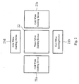
- Fig. 2 is a schematic view of an emitting module.
- the emitting module shown in Fig. 2 is a flat emitting module with chip on board (COB).
- the emitting devices 21a, 21b, 21c and 21 d are cold white emitting devices.
- the emitting device 22 is a warm white emitting device.
- the cold white emitting devices 21a, 21b, 21c and 21d are distributed around the warm white emitting device 22.
- the control circuit controls the turn-on and turn-off of the cold white emitting devices and the warm white emitting device for changing the color temperatures.
- the control circuit 11 includes a control signal generation device 13.
- the control signal generation device 13 generates a first control signal S1 and a second control signal S2 to control the first emitting device 14 and the second emitting device 15, wherein the second control signal S2 is generated according to the first control signal S1 and a compensation signal 16.
- the control circuit 11 may adjust the amplitude and duty cycle of the first control signal S1 and the second control signal S2 to control the brightness and turn-on time of the first emitting device 14 and the second emitting device 15.
- the emitting efficiency of the first emitting device 14 is different from the emitting efficiency of the second emitting device 15; for example, the first emitting efficiency is greater than the second emitting efficiency.
- the compensation signal 16 may be generated according to a difference between a first emitting efficiency of the first emitting device 14 and a second emitting efficiency of the second emitting device 15, and then the second control signal S2 is generated through the compensation signal 16 and the first control signal S1.
- a first light flux generated by the first emitting device 14 may be equivalent to a second light flux generated by the second emitting device 15.
- Fig. 3 is a schematic view of a control circuit according to an embodiment of the invention.
- the control circuit includes a pulse signal generation device 31 (e.g., a pulse width modulation (PWM) circuit), a buffer 32, an inverter 33 and a compensation device 34.
- the control circuit outputs the first control signal S1 and the second control signal S2 at the same time to control a first emitting device and a second emitting device.
- the pulse signal generation device 31 generates the first control signal S1, wherein the duty cycle of the first control signal S1 is determined according to a color temperature.
- the pulse signal generation device 31 comprises an oscillator 311, and the duty cycle of the first control signal is predetermined.
- the first control signal S1 is transferred to the buffer 32 and the inverter 33 respectively.
- the buffer 32 delays a predetermined time of the first control signal S1, so that the first control signal S1 outputted by the buffer 32 is synchronized with the second control signal S2 outputted by the compensation device 34.
- the predetermined time may be determined according to the processing speed of the inverter 33 and the compensation device 34.
- the inverter 33 makes an inverted processing to the first control signal S1 to generate and transfer an inverted first control signal S1' to the compensation device 34.
- the compensation device 34 outputs the second control signal S2 after it receives the inverted first control signal S1' and a compensation signal 35.
- the emitting efficiency of the first emitting device is different from the emitting efficiency of the second emitting device.
- the compensation device 34 may modify the inverted first control signal S1' according to the compensation signal 35 for reaching the foregoing purpose.
- the compensation signal 35 is generated according to a difference between the emitting efficiency of the first emitting device and the emitting efficiency of the second emitting device.
- the first emitting device is the cold white emitting device
- the second emitting device is the warm white emitting device. Since the emitting efficiency of the warm white emitting device is poorer, the compensation device 34 compensates the insufficient part of the emitting efficiency of the warm white emitting device.
- the compensation device 34 for changing the first control signal S1 transferred to the cold white emitting device so as to decrease the excessive part of the emitting efficiency of the cold white emitting device.
- the compensation device 34 is a DC level adjustment circuit
- the compensation signal is a DC bias compensation value
- the compensation device 34 adjusts a low voltage level of the inverted first control signal according to the DC bias compensation value.
- Fig. 4 is a schematic view of a control circuit according to a further embodiment of the invention.
- the control circuit includes a pulse signal generation device 41 (e.g., a PWM circuit), a buffer 42, an inverter 43 and an OR gate 44.
- the control circuit outputs the first control signal S1 and the second control signal S2 at the same time to control a first emitting device and a second emitting device.
- the pulse signal generation device 41 generates the first control signal S1, wherein the duty cycle of the first control signal S1 is determined according to a color temperature.
- the first control signal S1 is transferred to the buffer 42 and the inverter 43 respectively.
- the buffer 42 delays a predetermined time of the first control signal S1, so that the first control signal S1 outputted by the buffer 42 is synchronized with the second control signal S2 outputted by the OR gate 44.
- the predetermined time may be determined according to the processing speed of the inverter 43 and the OR gate 44.
- the inverter 43 makes the inverted processing to the first control signal S1 to generate and transfer an inverted first control signal S1' to the OR gate 44.
- the OR gate 44 makes an OR operation after it receives the inverted first control signal S1' and a compensation signal 45 to output the second control signal S2.
- the emitting efficiency of the first emitting device is different from the emitting efficiency of the second emitting device.
- the OR gate 44 may modify the inverted first control signal S1' according to the compensation signal 45 for reaching the foregoing purpose.
- the compensation signal 45 is generated according to a difference between the emitting efficiency of the first emitting device and the emitting efficiency of the second emitting device.
- the first emitting device is the cold white emitting device
- the second emitting device is the warm white emitting device. Since the emitting efficiency of the warm white emitting device is poorer, the OR gate 44 makes the OR operation to the inverted first control signal S1' and a compensation signal 45 for compensating the insufficient part of the emitting efficiency of the warm white emitting device.
- those skilled in the art also may design the OR gate 44 for changing the first control signal S1 transferred to the cold white emitting device so as to decrease the excessive part of the emitting efficiency of the cold white emitting device.
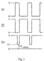
- Fig. 5 is a schematic view of a control signal generated according to an embodiment of the invention.
- the control signal generation device outputs the first control signal S1
- an inverter makes the inverted processing to the first control signal S1 for generating the inverted first control signal S 1 .
- a compensator may generate a DC voltage offset according to a difference between the emitting efficiency of two emitting devices.
- the compensator adjusts the low voltage level of the inverted first control signal S 1 to a voltage V1 according to the DC voltage offset for generating the second control signal S2.
- the second emitting device with a lower emitting efficiency may generate a light flux equivalent to the light flux of the first emitting device.
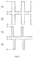
- Fig. 6 is a schematic view of a control signal generated according to a further embodiment of the invention.
- the control signal generation device outputs the first control signal S1
- an inverter makes the inverted processing to the first control signal S1 for generating the inverted first control signal S 1 .
- a compensation signal Sc is generated according to a difference between the emitting efficiency of the first emitting device and the emitting efficiency of the second emitting device.
- the compensator makes the OR operation to the inverted first control signal S 1 and the compensation signal Sc for generating the second control signal S2.
- the second emitting device with a lower emitting efficiency may generate a light flux equivalent to the light flux of the first emitting device.
- Fig. 7 is a schematic view of a lamp for use with an embodiment of the invention.
- the lamp includes a control signal generation device 71, a driving circuit 72 and an emitting module 73.
- the emitting module 73 includes a first emitting device 74 and a second emitting device 75.
- the first emitting device 74 is a cold white emitting device.
- the second emitting device 75 is a warm white emitting device.
- the first emitting device 74 and the second emitting device 75 may include one LED or a plurality of LEDs.
- the emitting module 73 only takes two emitting devices with different color temperatures for example, but the invention is not limited to this.
- the emitting module 73 may include more than two emitting devices. Each emitting device has a different color temperature.
- the control circuit 71 controls the driving device 72 to drive different emitting devices for changing the color temperature of the lamp.
- the control signal generation device 71 generates a first control signal S1, and a second control signal S2 is generated according to the first control signal S1 and a compensation signal 76.
- the driving device 72 outputs a corresponding first driving signal SD1 and a second driving signal SD2 after it receives the first control signal S1 and the second control signal S2 so as to drive the first emitting device 74 and the second emitting device 75.
- the control signal generation device 71 may adjust the amplitude and duty cycle of the first control signal S1 and the second control signal S2 to change the voltage, current or turn-on time of the first driving signal SD1 and the second driving signal SD2, thereby controlling the brightness and turn-on time of the first emitting device 74 and the second emitting device 75.
- the emitting efficiency of the first emitting device 74 is different from the emitting efficiency of the second emitting device 75. Therefore, the compensation signal 76 may be generated according to a difference between a first emitting efficiency of the first emitting device 74 and a second emitting efficiency of the second emitting device 75, and then the second control signal S2 is generated through the compensation signal 76 and the first control signal S1.
- the driving circuit 72 is controlled by means of the above-mentioned control signal generation mode, so that a first light flux generated by the first emitting device 74 is equivalent to a second light flux of the second emitting device 75.
Landscapes
- Circuit Arrangement For Electric Light Sources In General (AREA)
Description
- This application claims priority to Taiwan Application Serial Number
100137648, filed October 18, 2011 - The invention relates to a lamp. More particularly the invention relates to a lamp having color temperature adjustment.
- Light emitting diodes used in electronic components in the past have been widely used in lighting products currently. Since the light emitting diodes have excellent electrical property and structural feature, a demand for the light emitting diodes has been increased gradually. Compared to fluorescent lamps and incandescent lamps, white LEDs have attracted great attention. However, corresponding to different demands of users, a lamp which can meet the demand for generating lights with different color temperatures is generated consequently. However, the color temperatures of conventional LEDs have been determined before leaving the factory and can not be changed. If users have a demand for lights with different color temperatures, the demand can only be solved by replacing LEDs having different color temperatures. This is inconvenient for users.
-
WO 2011/093395 A1 discloses a light control apparatus for a white LED light-emitting device. - In an example useful for understanding the present invention, a lamp or lighting system capable of controlling a color temperature is provided.
- The invention provides a control circuit, which can control emitting devices with different color temperatures in a lamp, and the color temperature of the whole lamp is adjusted through a control signal outputted by the control circuit.
- The control circuit provided by the invention only requires a single control signal generator, and then at least two different control signals are generated by other circuits, to decrease the layout area and cost of the control circuit.
- Other purposes and advantages of the invention may be further understood from the technical characteristics disclosed by the invention.
- For realizing one purpose or a part of or all of the purposes described above or other purposes, a lamp for use with an embodiment of the invention is provided, including a first emitting device, a second emitting device and a control signal generation device. The control signal generation device generates a first control signal and a second control signal to control the first emitting device and the second emitting device, so that a first light flux generated by the first emitting device is equivalent to a second light flux generated by the second emitting device, wherein the second control signal is generated according to the first control signal.
- An embodiment of the invention provides a control circuit as recited in
claim 1. -
-
Fig. 1 is a schematic view of a lamp comprising a control circuit according to an embodiment of the invention; -
Fig. 2 is a schematic view of an emitting module; -
Fig. 3 is a schematic view of a control circuit according to an embodiment of the invention; -
Fig. 4 is a schematic view of a control circuit according to a further embodiment of the invention; -
Fig. 5 is a schematic view of a control signal generated according to an embodiment of the invention; -
Fig. 6 is a schematic view of a control signal generated according to a further embodiment of the invention; and -
Fig. 7 is a schematic view of a lamp for use with an embodiment of the invention. - The foregoing and other technical contents, features and functions of the invention may be clearly shown in the following detailed description of a preferred embodiment with reference to the drawings. Directional terms mentioned in the following embodiments, such as up, down, left, right, front or back, only refer to the directions of the accompany drawings. Therefore, the directional terms used herein are only used to illustrate the invention and are not limitative.
-
Fig. 1 is a schematic view of a lamp comprising a control circuit according to an embodiment of the invention. The lamp includes acontrol circuit 11 and anemitting module 12. Theemitting module 12 includes afirst emitting device 14 and asecond emitting device 15. Thefirst emitting device 14 is a cold white emitting device. Thesecond emitting device 15 is a warm white emitting device. In the embodiment, thefirst emitting device 14 and thesecond emitting device 15 may include one LED or a plurality of LEDs. In the embodiment, theemitting module 12 only takes two emitting devices with different color temperatures for examples for illustration, but the invention is not limited to this. Theemitting module 12 may include more than two emitting devices. Each emitting device has a different color temperature. Then, thecontrol circuit 11 controls different emitting devices to change the color temperature of the lamp. The arrangement of thefirst emitting device 14 and thesecond emitting device 15 in theemitting module 12 may have some variations according to a demand of a designer. Referring toFig. 2., Fig. 2 is a schematic view of an emitting module. The emitting module shown inFig. 2 is a flat emitting module with chip on board (COB). Theemitting devices emitting device 22 is a warm white emitting device. The coldwhite emitting devices white emitting device 22. Then, the control circuit controls the turn-on and turn-off of the cold white emitting devices and the warm white emitting device for changing the color temperatures. - The
control circuit 11 includes a controlsignal generation device 13. The controlsignal generation device 13 generates a first control signal S1 and a second control signal S2 to control thefirst emitting device 14 and thesecond emitting device 15, wherein the second control signal S2 is generated according to the first control signal S1 and a compensation signal 16. Thecontrol circuit 11 may adjust the amplitude and duty cycle of the first control signal S1 and the second control signal S2 to control the brightness and turn-on time of thefirst emitting device 14 and thesecond emitting device 15. In the embodiment, the emitting efficiency of thefirst emitting device 14 is different from the emitting efficiency of thesecond emitting device 15; for example, the first emitting efficiency is greater than the second emitting efficiency. Therefore, the compensation signal 16 may be generated according to a difference between a first emitting efficiency of thefirst emitting device 14 and a second emitting efficiency of thesecond emitting device 15, and then the second control signal S2 is generated through the compensation signal 16 and the first control signal S1. By means of the above-mentioned control signal generation mode, a first light flux generated by thefirst emitting device 14 may be equivalent to a second light flux generated by thesecond emitting device 15. -
Fig. 3 is a schematic view of a control circuit according to an embodiment of the invention. The control circuit includes a pulse signal generation device 31 (e.g., a pulse width modulation (PWM) circuit), abuffer 32, aninverter 33 and acompensation device 34. The control circuit outputs the first control signal S1 and the second control signal S2 at the same time to control a first emitting device and a second emitting device. The pulsesignal generation device 31 generates the first control signal S1, wherein the duty cycle of the first control signal S1 is determined according to a color temperature. The pulsesignal generation device 31 comprises anoscillator 311, and the duty cycle of the first control signal is predetermined. The first control signal S1 is transferred to thebuffer 32 and theinverter 33 respectively. Thebuffer 32 delays a predetermined time of the first control signal S1, so that the first control signal S1 outputted by thebuffer 32 is synchronized with the second control signal S2 outputted by thecompensation device 34. The predetermined time may be determined according to the processing speed of theinverter 33 and thecompensation device 34. Theinverter 33 makes an inverted processing to the first control signal S1 to generate and transfer an inverted first control signal S1' to thecompensation device 34. Thecompensation device 34 outputs the second control signal S2 after it receives the inverted first control signal S1' and acompensation signal 35. In the embodiment, the emitting efficiency of the first emitting device is different from the emitting efficiency of the second emitting device. In order to make the light flux generated by the first emitting device equivalent to the light flux generated by the second emitting device, thecompensation device 34 may modify the inverted first control signal S1' according to thecompensation signal 35 for reaching the foregoing purpose. In the embodiment, thecompensation signal 35 is generated according to a difference between the emitting efficiency of the first emitting device and the emitting efficiency of the second emitting device. In the embodiment, the first emitting device is the cold white emitting device, and the second emitting device is the warm white emitting device. Since the emitting efficiency of the warm white emitting device is poorer, thecompensation device 34 compensates the insufficient part of the emitting efficiency of the warm white emitting device. However, those skilled in the art also may design thecompensation device 34 for changing the first control signal S1 transferred to the cold white emitting device so as to decrease the excessive part of the emitting efficiency of the cold white emitting device. In one embodiment, thecompensation device 34 is a DC level adjustment circuit, the compensation signal is a DC bias compensation value, and thecompensation device 34 adjusts a low voltage level of the inverted first control signal according to the DC bias compensation value. -
Fig. 4 is a schematic view of a control circuit according to a further embodiment of the invention. The control circuit includes a pulse signal generation device 41 (e.g., a PWM circuit), abuffer 42, aninverter 43 and anOR gate 44. The control circuit outputs the first control signal S1 and the second control signal S2 at the same time to control a first emitting device and a second emitting device. The pulsesignal generation device 41 generates the first control signal S1, wherein the duty cycle of the first control signal S1 is determined according to a color temperature. The first control signal S1 is transferred to thebuffer 42 and theinverter 43 respectively. Thebuffer 42 delays a predetermined time of the first control signal S1, so that the first control signal S1 outputted by thebuffer 42 is synchronized with the second control signal S2 outputted by theOR gate 44. The predetermined time may be determined according to the processing speed of theinverter 43 and theOR gate 44. Theinverter 43 makes the inverted processing to the first control signal S1 to generate and transfer an inverted first control signal S1' to theOR gate 44. TheOR gate 44 makes an OR operation after it receives the inverted first control signal S1' and acompensation signal 45 to output the second control signal S2. In the embodiment, the emitting efficiency of the first emitting device is different from the emitting efficiency of the second emitting device. In order to make the light flux generated by the first emitting device equivalent to the light flux generated by the second emitting device, theOR gate 44 may modify the inverted first control signal S1' according to thecompensation signal 45 for reaching the foregoing purpose. In the embodiment, thecompensation signal 45 is generated according to a difference between the emitting efficiency of the first emitting device and the emitting efficiency of the second emitting device. In the embodiment, the first emitting device is the cold white emitting device, and the second emitting device is the warm white emitting device. Since the emitting efficiency of the warm white emitting device is poorer, theOR gate 44 makes the OR operation to the inverted first control signal S1' and acompensation signal 45 for compensating the insufficient part of the emitting efficiency of the warm white emitting device. However, those skilled in the art also may design theOR gate 44 for changing the first control signal S1 transferred to the cold white emitting device so as to decrease the excessive part of the emitting efficiency of the cold white emitting device. - In order to illustrate the operation of the first control signal, the second control signal and the compensation signal more clearly,
Figs. 5 and6 are referred to.Fig. 5 is a schematic view of a control signal generated according to an embodiment of the invention. After the control signal generation device outputs the first control signal S1, firstly an inverter makes the inverted processing to the first control signal S1 for generating the inverted first control signalS1 . Then, a compensator may generate a DC voltage offset according to a difference between the emitting efficiency of two emitting devices. Afterwards, the compensator adjusts the low voltage level of the inverted first control signalS1 to a voltage V1 according to the DC voltage offset for generating the second control signal S2. In such a way, the second emitting device with a lower emitting efficiency may generate a light flux equivalent to the light flux of the first emitting device. -
Fig. 6 is a schematic view of a control signal generated according to a further embodiment of the invention. After the control signal generation device outputs the first control signal S1, firstly an inverter makes the inverted processing to the first control signal S1 for generating the inverted first control signalS1 . Then, a compensation signal Sc is generated according to a difference between the emitting efficiency of the first emitting device and the emitting efficiency of the second emitting device. Afterwards, the compensator makes the OR operation to the inverted first control signalS1 and the compensation signal Sc for generating the second control signal S2. In such a way, the second emitting device with a lower emitting efficiency may generate a light flux equivalent to the light flux of the first emitting device. -
Fig. 7 is a schematic view of a lamp for use with an embodiment of the invention. The lamp includes a control signal generation
device 71, a drivingcircuit 72 and an emittingmodule 73. The emittingmodule 73 includes a first emittingdevice 74 and a second emittingdevice 75. The first emittingdevice 74 is a cold white emitting device. The second emittingdevice 75 is a warm white emitting device. In the embodiment, the first emittingdevice 74 and the second emittingdevice 75 may include one LED or a plurality of LEDs. In the embodiment, the emittingmodule 73 only takes two emitting devices with different color temperatures for example, but the invention is not limited to this. The emittingmodule 73 may include more than two emitting devices. Each emitting device has a different color temperature. Then, thecontrol circuit 71 controls the drivingdevice 72 to drive different emitting devices for changing the color temperature of the lamp. - The control
signal generation device 71 generates a first control signal S1, and a second control signal S2 is generated according to the first control signal S1 and a compensation signal 76. The drivingdevice 72 outputs a corresponding first driving signal SD1 and a second driving signal SD2 after it receives the first control signal S1 and the second control signal S2 so as to drive the first emittingdevice 74 and the second emittingdevice 75. The controlsignal generation device 71 may adjust the amplitude and duty cycle of the first control signal S1 and the second control signal S2 to change the voltage, current or turn-on time of the first driving signal SD1 and the second driving signal SD2, thereby controlling the brightness and turn-on time of the first emittingdevice 74 and the second emittingdevice 75. In the embodiment, the emitting efficiency of the first emittingdevice 74 is different from the emitting efficiency of the second emittingdevice 75. Therefore, the compensation signal 76 may be generated according to a difference between a first emitting efficiency of the first emittingdevice 74 and a second emitting efficiency of the second emittingdevice 75, and then the second control signal S2 is generated through the compensation signal 76 and the first control signal S1. The drivingcircuit 72 is controlled by means of the above-mentioned control signal generation mode, so that a first light flux generated by the first emittingdevice 74 is equivalent to a second light flux of the second emittingdevice 75.
Claims (7)
- A control circuit (11) adapted to control a color temperature of a lamp, comprising:a pulse signal generation device (31, 41) adapted to generate a first control signal;a buffer device (32, 42) adapted to receive and buffer the first control signal and generate a buffered first control signal (S1);an inverter (33, 43) adapted to receive the first control signal to generate an inverted first control signal (S1'); anda compensation device (34, 44) adapted to receive a compensation signal (16, 35, 45, 76) and the inverted first control signal (S1') and to generate a second control signal (S2) according to said compensation signal and said inverted first control signal, wherein the buffered first control signal (S1) controls a first emitting device (14, 74) in the lamp and the second control signal (S2) controls a second emitting device (15, 75) in the lamp.
- The control circuit of claim 1, wherein the compensation signal (16, 35, 45, 76) is generated according to emitting efficiency of the first emitting device (14, 74) and the second emitting device (15, 75).
- The control circuit of claim 1, wherein the pulse signal generation device (31, 41) comprises an oscillator (311), and a duty cycle of the first control signal (S1) is set according to the color temperature.
- The control circuit of claim 1, wherein the buffer device (32, 42) is adapted to synchronize the first control signal (S1) with the second control signal (S2).
- The control circuit of claim 1, wherein the compensation signal (16, 35, 45, 76) is generated according to a difference between a first emitting efficiency of the first emitting device (14, 74) and a second emitting efficiency of the second emitting device (15, 75).
- The control circuit of claim 1, wherein the compensation device (34, 44) is a DC level adjustment circuit, the compensation signal (16, 35, 45, 76) is a DC bias compensation value, and the compensation device (34, 44) is adapted to adjust a low voltage level of the inverted first control signal (S1') according to the DC bias compensation value.
- The control circuit of claim 1, further comprising a driving device (72) adapted to receive the first control signal (S1) and the second control (S2) signal to drive the first emitting device (14, 74) and the second emitting device (15, 75).
Applications Claiming Priority (1)
| Application Number | Priority Date | Filing Date | Title |
|---|---|---|---|
| TW100137648A TWI442827B (en) | 2011-10-18 | 2011-10-18 | Lamps and control circuit |
Publications (2)
| Publication Number | Publication Date |
|---|---|
| EP2584869A1 EP2584869A1 (en) | 2013-04-24 |
| EP2584869B1 true EP2584869B1 (en) | 2016-11-23 |
Family
ID=47040588
Family Applications (1)
| Application Number | Title | Priority Date | Filing Date |
|---|---|---|---|
| EP12189039.6A Not-in-force EP2584869B1 (en) | 2011-10-18 | 2012-10-18 | Lamps and control circuit |
Country Status (4)
| Country | Link |
|---|---|
| US (1) | US8981669B2 (en) |
| EP (1) | EP2584869B1 (en) |
| CN (1) | CN103068101A (en) |
| TW (1) | TWI442827B (en) |
Families Citing this family (1)
| Publication number | Priority date | Publication date | Assignee | Title |
|---|---|---|---|---|
| KR102227773B1 (en) | 2014-10-21 | 2021-03-16 | 삼성전자주식회사 | Light emitting device |
Family Cites Families (10)
| Publication number | Priority date | Publication date | Assignee | Title |
|---|---|---|---|---|
| CN101128979B (en) * | 2004-10-12 | 2011-10-19 | 皇家飞利浦电子股份有限公司 | High precision control apparatus and method for use with modulated light sources |
| KR100728134B1 (en) * | 2005-12-30 | 2007-06-13 | 김재조 | Light emitting device |
| US8044612B2 (en) * | 2007-01-30 | 2011-10-25 | Cypress Semiconductor Corporation | Method and apparatus for networked illumination devices |
| US8203260B2 (en) | 2007-04-13 | 2012-06-19 | Intematix Corporation | Color temperature tunable white light source |
| BRPI0821978A2 (en) * | 2008-01-17 | 2015-07-21 | Koninkl Philips Electronics Nv | Lighting unit, method for generating light, and, computer program product |
| US8339029B2 (en) * | 2009-02-19 | 2012-12-25 | Cree, Inc. | Light emitting devices and systems having tunable chromaticity |
| CN101697654B (en) * | 2009-10-30 | 2013-02-27 | 中山大学 | Correlated color temperature and color rendering index self-calibration circuit of LED light source composed of multiple light colors |
| EP2531008A4 (en) | 2010-01-29 | 2014-06-04 | Mitsubishi Chem Corp | LIGHT CONTROL APPARATUS FOR A WHITE LED LIGHT EMITTING DEVICE, AND LIGHTING SYSTEM |
| CN102200247A (en) | 2010-03-24 | 2011-09-28 | 富准精密工业(深圳)有限公司 | Light emitting diode lamp |
| CN201925771U (en) * | 2010-12-16 | 2011-08-10 | 唐万华 | A lamp with adjustable luminous flux and color temperature |
-
2011
- 2011-10-18 TW TW100137648A patent/TWI442827B/en not_active IP Right Cessation
- 2011-12-29 CN CN201110451057XA patent/CN103068101A/en active Pending
-
2012
- 2012-10-17 US US13/653,560 patent/US8981669B2/en not_active Expired - Fee Related
- 2012-10-18 EP EP12189039.6A patent/EP2584869B1/en not_active Not-in-force
Also Published As
| Publication number | Publication date |
|---|---|
| EP2584869A1 (en) | 2013-04-24 |
| TW201318475A (en) | 2013-05-01 |
| US8981669B2 (en) | 2015-03-17 |
| CN103068101A (en) | 2013-04-24 |
| US20130093344A1 (en) | 2013-04-18 |
| TWI442827B (en) | 2014-06-21 |
Similar Documents
| Publication | Publication Date | Title |
|---|---|---|
| US7872430B2 (en) | Solid state lighting panels with variable voltage boost current sources | |
| JP5141874B2 (en) | Lighting device | |
| US20110025230A1 (en) | Driver device for leds | |
| CN102238768B (en) | Light emitting diode backlight source driving module | |
| EP1949765B1 (en) | Solid state lighting panels with variable voltage boost current sources | |
| US9072142B2 (en) | LED lighting unit with color and dimming control | |
| CN102905443B (en) | Linear constant-current and current-sharing LED drive circuit and circuit board structure thereof | |
| KR20100040941A (en) | Correction of temperature induced color drift in solid state lighting displays | |
| WO2019198604A1 (en) | Vehicle lamp, lighting circuit therefor, driver circuit, and driver-integrated light source | |
| US9585218B2 (en) | Lighting apparatus with variable current switching frequency and methods of operating same | |
| CN102201198A (en) | Circuit and method for generating PWM signal and LED driving circuit | |
| TWI478620B (en) | Light-emitting diode backlight system, driving device and driving method thereof | |
| US8525422B2 (en) | Backlight apparatus | |
| US20120049760A1 (en) | Apparatus and methods for dimming illumination devices | |
| KR20140092383A (en) | Lighting device including a drive device configured for dimming light - emitting diodes in response to voltage and temperature | |
| US8981669B2 (en) | Lamps and control circuit | |
| CN211181603U (en) | Light-emitting circuit, backlight module and display | |
| CN102903339B (en) | The control method of backlight sources of display device and control device | |
| US20100156775A1 (en) | Electronic apparatus and backlight unit for the same | |
| US8816590B2 (en) | Lighting device with adjustable color temperature | |
| CN101998725A (en) | Drive circuit of light-emitting diode | |
| KR20110130988A (en) | Driving device of the lamp | |
| JP2012221714A (en) | Power supply and luminaire | |
| US20120049750A1 (en) | Light emitting diode driving method | |
| JP6816354B2 (en) | Lighting device |
Legal Events
| Date | Code | Title | Description |
|---|---|---|---|
| PUAI | Public reference made under article 153(3) epc to a published international application that has entered the european phase |
Free format text: ORIGINAL CODE: 0009012 |
|
| AK | Designated contracting states |
Kind code of ref document: A1 Designated state(s): AL AT BE BG CH CY CZ DE DK EE ES FI FR GB GR HR HU IE IS IT LI LT LU LV MC MK MT NL NO PL PT RO RS SE SI SK SM TR |
|
| AX | Request for extension of the european patent |
Extension state: BA ME |
|
| 17P | Request for examination filed |
Effective date: 20130917 |
|
| RBV | Designated contracting states (corrected) |
Designated state(s): AL AT BE BG CH CY CZ DE DK EE ES FI FR GB GR HR HU IE IS IT LI LT LU LV MC MK MT NL NO PL PT RO RS SE SI SK SM TR |
|
| 17Q | First examination report despatched |
Effective date: 20150612 |
|
| GRAP | Despatch of communication of intention to grant a patent |
Free format text: ORIGINAL CODE: EPIDOSNIGR1 |
|
| INTG | Intention to grant announced |
Effective date: 20160509 |
|
| GRAS | Grant fee paid |
Free format text: ORIGINAL CODE: EPIDOSNIGR3 |
|
| GRAA | (expected) grant |
Free format text: ORIGINAL CODE: 0009210 |
|
| AK | Designated contracting states |
Kind code of ref document: B1 Designated state(s): AL AT BE BG CH CY CZ DE DK EE ES FI FR GB GR HR HU IE IS IT LI LT LU LV MC MK MT NL NO PL PT RO RS SE SI SK SM TR |
|
| REG | Reference to a national code |
Ref country code: GB Ref legal event code: FG4D |
|
| REG | Reference to a national code |
Ref country code: CH Ref legal event code: EP |
|
| REG | Reference to a national code |
Ref country code: IE Ref legal event code: FG4D |
|
| REG | Reference to a national code |
Ref country code: AT Ref legal event code: REF Ref document number: 848891 Country of ref document: AT Kind code of ref document: T Effective date: 20161215 |
|
| REG | Reference to a national code |
Ref country code: DE Ref legal event code: R096 Ref document number: 602012025660 Country of ref document: DE |
|
| PG25 | Lapsed in a contracting state [announced via postgrant information from national office to epo] |
Ref country code: LV Free format text: LAPSE BECAUSE OF FAILURE TO SUBMIT A TRANSLATION OF THE DESCRIPTION OR TO PAY THE FEE WITHIN THE PRESCRIBED TIME-LIMIT Effective date: 20161123 |
|
| REG | Reference to a national code |
Ref country code: LT Ref legal event code: MG4D |
|
| REG | Reference to a national code |
Ref country code: NL Ref legal event code: MP Effective date: 20161123 |
|
| REG | Reference to a national code |
Ref country code: AT Ref legal event code: MK05 Ref document number: 848891 Country of ref document: AT Kind code of ref document: T Effective date: 20161123 |
|
| PG25 | Lapsed in a contracting state [announced via postgrant information from national office to epo] |
Ref country code: NO Free format text: LAPSE BECAUSE OF FAILURE TO SUBMIT A TRANSLATION OF THE DESCRIPTION OR TO PAY THE FEE WITHIN THE PRESCRIBED TIME-LIMIT Effective date: 20170223 Ref country code: LT Free format text: LAPSE BECAUSE OF FAILURE TO SUBMIT A TRANSLATION OF THE DESCRIPTION OR TO PAY THE FEE WITHIN THE PRESCRIBED TIME-LIMIT Effective date: 20161123 Ref country code: GR Free format text: LAPSE BECAUSE OF FAILURE TO SUBMIT A TRANSLATION OF THE DESCRIPTION OR TO PAY THE FEE WITHIN THE PRESCRIBED TIME-LIMIT Effective date: 20170224 Ref country code: SE Free format text: LAPSE BECAUSE OF FAILURE TO SUBMIT A TRANSLATION OF THE DESCRIPTION OR TO PAY THE FEE WITHIN THE PRESCRIBED TIME-LIMIT Effective date: 20161123 Ref country code: NL Free format text: LAPSE BECAUSE OF FAILURE TO SUBMIT A TRANSLATION OF THE DESCRIPTION OR TO PAY THE FEE WITHIN THE PRESCRIBED TIME-LIMIT Effective date: 20161123 |
|
| PG25 | Lapsed in a contracting state [announced via postgrant information from national office to epo] |
Ref country code: AT Free format text: LAPSE BECAUSE OF FAILURE TO SUBMIT A TRANSLATION OF THE DESCRIPTION OR TO PAY THE FEE WITHIN THE PRESCRIBED TIME-LIMIT Effective date: 20161123 Ref country code: FI Free format text: LAPSE BECAUSE OF FAILURE TO SUBMIT A TRANSLATION OF THE DESCRIPTION OR TO PAY THE FEE WITHIN THE PRESCRIBED TIME-LIMIT Effective date: 20161123 Ref country code: ES Free format text: LAPSE BECAUSE OF FAILURE TO SUBMIT A TRANSLATION OF THE DESCRIPTION OR TO PAY THE FEE WITHIN THE PRESCRIBED TIME-LIMIT Effective date: 20161123 Ref country code: PT Free format text: LAPSE BECAUSE OF FAILURE TO SUBMIT A TRANSLATION OF THE DESCRIPTION OR TO PAY THE FEE WITHIN THE PRESCRIBED TIME-LIMIT Effective date: 20170323 Ref country code: PL Free format text: LAPSE BECAUSE OF FAILURE TO SUBMIT A TRANSLATION OF THE DESCRIPTION OR TO PAY THE FEE WITHIN THE PRESCRIBED TIME-LIMIT Effective date: 20161123 Ref country code: HR Free format text: LAPSE BECAUSE OF FAILURE TO SUBMIT A TRANSLATION OF THE DESCRIPTION OR TO PAY THE FEE WITHIN THE PRESCRIBED TIME-LIMIT Effective date: 20161123 Ref country code: RS Free format text: LAPSE BECAUSE OF FAILURE TO SUBMIT A TRANSLATION OF THE DESCRIPTION OR TO PAY THE FEE WITHIN THE PRESCRIBED TIME-LIMIT Effective date: 20161123 |
|
| PG25 | Lapsed in a contracting state [announced via postgrant information from national office to epo] |
Ref country code: RO Free format text: LAPSE BECAUSE OF FAILURE TO SUBMIT A TRANSLATION OF THE DESCRIPTION OR TO PAY THE FEE WITHIN THE PRESCRIBED TIME-LIMIT Effective date: 20161123 Ref country code: EE Free format text: LAPSE BECAUSE OF FAILURE TO SUBMIT A TRANSLATION OF THE DESCRIPTION OR TO PAY THE FEE WITHIN THE PRESCRIBED TIME-LIMIT Effective date: 20161123 Ref country code: DK Free format text: LAPSE BECAUSE OF FAILURE TO SUBMIT A TRANSLATION OF THE DESCRIPTION OR TO PAY THE FEE WITHIN THE PRESCRIBED TIME-LIMIT Effective date: 20161123 Ref country code: CZ Free format text: LAPSE BECAUSE OF FAILURE TO SUBMIT A TRANSLATION OF THE DESCRIPTION OR TO PAY THE FEE WITHIN THE PRESCRIBED TIME-LIMIT Effective date: 20161123 Ref country code: SK Free format text: LAPSE BECAUSE OF FAILURE TO SUBMIT A TRANSLATION OF THE DESCRIPTION OR TO PAY THE FEE WITHIN THE PRESCRIBED TIME-LIMIT Effective date: 20161123 |
|
| REG | Reference to a national code |
Ref country code: DE Ref legal event code: R097 Ref document number: 602012025660 Country of ref document: DE |
|
| PG25 | Lapsed in a contracting state [announced via postgrant information from national office to epo] |
Ref country code: SM Free format text: LAPSE BECAUSE OF FAILURE TO SUBMIT A TRANSLATION OF THE DESCRIPTION OR TO PAY THE FEE WITHIN THE PRESCRIBED TIME-LIMIT Effective date: 20161123 Ref country code: BG Free format text: LAPSE BECAUSE OF FAILURE TO SUBMIT A TRANSLATION OF THE DESCRIPTION OR TO PAY THE FEE WITHIN THE PRESCRIBED TIME-LIMIT Effective date: 20170223 Ref country code: BE Free format text: LAPSE BECAUSE OF FAILURE TO SUBMIT A TRANSLATION OF THE DESCRIPTION OR TO PAY THE FEE WITHIN THE PRESCRIBED TIME-LIMIT Effective date: 20161123 |
|
| REG | Reference to a national code |
Ref country code: FR Ref legal event code: PLFP Year of fee payment: 6 |
|
| PLBE | No opposition filed within time limit |
Free format text: ORIGINAL CODE: 0009261 |
|
| STAA | Information on the status of an ep patent application or granted ep patent |
Free format text: STATUS: NO OPPOSITION FILED WITHIN TIME LIMIT |
|
| 26N | No opposition filed |
Effective date: 20170824 |
|
| PG25 | Lapsed in a contracting state [announced via postgrant information from national office to epo] |
Ref country code: SI Free format text: LAPSE BECAUSE OF FAILURE TO SUBMIT A TRANSLATION OF THE DESCRIPTION OR TO PAY THE FEE WITHIN THE PRESCRIBED TIME-LIMIT Effective date: 20161123 |
|
| PG25 | Lapsed in a contracting state [announced via postgrant information from national office to epo] |
Ref country code: MC Free format text: LAPSE BECAUSE OF FAILURE TO SUBMIT A TRANSLATION OF THE DESCRIPTION OR TO PAY THE FEE WITHIN THE PRESCRIBED TIME-LIMIT Effective date: 20161123 |
|
| REG | Reference to a national code |
Ref country code: CH Ref legal event code: PL |
|
| REG | Reference to a national code |
Ref country code: IE Ref legal event code: MM4A |
|
| PG25 | Lapsed in a contracting state [announced via postgrant information from national office to epo] |
Ref country code: LI Free format text: LAPSE BECAUSE OF NON-PAYMENT OF DUE FEES Effective date: 20171031 Ref country code: LU Free format text: LAPSE BECAUSE OF NON-PAYMENT OF DUE FEES Effective date: 20171018 Ref country code: CH Free format text: LAPSE BECAUSE OF NON-PAYMENT OF DUE FEES Effective date: 20171031 |
|
| REG | Reference to a national code |
Ref country code: FR Ref legal event code: PLFP Year of fee payment: 7 |
|
| PG25 | Lapsed in a contracting state [announced via postgrant information from national office to epo] |
Ref country code: MT Free format text: LAPSE BECAUSE OF NON-PAYMENT OF DUE FEES Effective date: 20171018 |
|
| PG25 | Lapsed in a contracting state [announced via postgrant information from national office to epo] |
Ref country code: IE Free format text: LAPSE BECAUSE OF NON-PAYMENT OF DUE FEES Effective date: 20171018 |
|
| PGFP | Annual fee paid to national office [announced via postgrant information from national office to epo] |
Ref country code: FR Payment date: 20180919 Year of fee payment: 7 |
|
| PGFP | Annual fee paid to national office [announced via postgrant information from national office to epo] |
Ref country code: GB Payment date: 20180919 Year of fee payment: 7 |
|
| PGFP | Annual fee paid to national office [announced via postgrant information from national office to epo] |
Ref country code: DE Payment date: 20180920 Year of fee payment: 7 |
|
| PGFP | Annual fee paid to national office [announced via postgrant information from national office to epo] |
Ref country code: IT Payment date: 20181029 Year of fee payment: 7 |
|
| PG25 | Lapsed in a contracting state [announced via postgrant information from national office to epo] |
Ref country code: HU Free format text: LAPSE BECAUSE OF FAILURE TO SUBMIT A TRANSLATION OF THE DESCRIPTION OR TO PAY THE FEE WITHIN THE PRESCRIBED TIME-LIMIT; INVALID AB INITIO Effective date: 20121018 |
|
| PG25 | Lapsed in a contracting state [announced via postgrant information from national office to epo] |
Ref country code: CY Free format text: LAPSE BECAUSE OF NON-PAYMENT OF DUE FEES Effective date: 20161123 |
|
| REG | Reference to a national code |
Ref country code: DE Ref legal event code: R079 Ref document number: 602012025660 Country of ref document: DE Free format text: PREVIOUS MAIN CLASS: H05B0033080000 Ipc: H05B0045000000 |
|
| PG25 | Lapsed in a contracting state [announced via postgrant information from national office to epo] |
Ref country code: MK Free format text: LAPSE BECAUSE OF FAILURE TO SUBMIT A TRANSLATION OF THE DESCRIPTION OR TO PAY THE FEE WITHIN THE PRESCRIBED TIME-LIMIT Effective date: 20161123 |
|
| PG25 | Lapsed in a contracting state [announced via postgrant information from national office to epo] |
Ref country code: TR Free format text: LAPSE BECAUSE OF FAILURE TO SUBMIT A TRANSLATION OF THE DESCRIPTION OR TO PAY THE FEE WITHIN THE PRESCRIBED TIME-LIMIT Effective date: 20161123 |
|
| REG | Reference to a national code |
Ref country code: DE Ref legal event code: R119 Ref document number: 602012025660 Country of ref document: DE |
|
| PG25 | Lapsed in a contracting state [announced via postgrant information from national office to epo] |
Ref country code: AL Free format text: LAPSE BECAUSE OF FAILURE TO SUBMIT A TRANSLATION OF THE DESCRIPTION OR TO PAY THE FEE WITHIN THE PRESCRIBED TIME-LIMIT Effective date: 20161123 Ref country code: DE Free format text: LAPSE BECAUSE OF NON-PAYMENT OF DUE FEES Effective date: 20200501 Ref country code: IS Free format text: LAPSE BECAUSE OF FAILURE TO SUBMIT A TRANSLATION OF THE DESCRIPTION OR TO PAY THE FEE WITHIN THE PRESCRIBED TIME-LIMIT Effective date: 20170323 |
|
| GBPC | Gb: european patent ceased through non-payment of renewal fee |
Effective date: 20191018 |
|
| PG25 | Lapsed in a contracting state [announced via postgrant information from national office to epo] |
Ref country code: IT Free format text: LAPSE BECAUSE OF NON-PAYMENT OF DUE FEES Effective date: 20191018 Ref country code: GB Free format text: LAPSE BECAUSE OF NON-PAYMENT OF DUE FEES Effective date: 20191018 Ref country code: FR Free format text: LAPSE BECAUSE OF NON-PAYMENT OF DUE FEES Effective date: 20191031 |