EP2584749A1 - Radio communication system, home gateway, bidirectional communication system, and method for stabilising a sideband signal - Google Patents
Radio communication system, home gateway, bidirectional communication system, and method for stabilising a sideband signal Download PDFInfo
- Publication number
- EP2584749A1 EP2584749A1 EP11290482.6A EP11290482A EP2584749A1 EP 2584749 A1 EP2584749 A1 EP 2584749A1 EP 11290482 A EP11290482 A EP 11290482A EP 2584749 A1 EP2584749 A1 EP 2584749A1
- Authority
- EP
- European Patent Office
- Prior art keywords
- signal
- carrier
- sub
- oscillator
- phase error
- Prior art date
- Legal status (The legal status is an assumption and is not a legal conclusion. Google has not performed a legal analysis and makes no representation as to the accuracy of the status listed.)
- Granted
Links
- 230000006854 communication Effects 0.000 title claims abstract description 87
- 238000000034 method Methods 0.000 title claims description 28
- 230000007175 bidirectional communication Effects 0.000 title claims description 19
- 230000003019 stabilising effect Effects 0.000 title claims description 8
- 238000001514 detection method Methods 0.000 claims abstract description 22
- 230000003287 optical effect Effects 0.000 claims description 42
- 238000001228 spectrum Methods 0.000 claims description 9
- 230000005540 biological transmission Effects 0.000 description 11
- 238000006243 chemical reaction Methods 0.000 description 11
- 230000006641 stabilisation Effects 0.000 description 11
- 230000003595 spectral effect Effects 0.000 description 10
- 230000008569 process Effects 0.000 description 8
- 239000000835 fiber Substances 0.000 description 6
- 230000001276 controlling effect Effects 0.000 description 5
- 238000001914 filtration Methods 0.000 description 5
- 239000013307 optical fiber Substances 0.000 description 3
- 230000035559 beat frequency Effects 0.000 description 2
- 230000008859 change Effects 0.000 description 2
- 238000004590 computer program Methods 0.000 description 2
- 239000000284 extract Substances 0.000 description 2
- 239000004065 semiconductor Substances 0.000 description 2
- 230000036962 time dependent Effects 0.000 description 2
- LZDYZEGISBDSDP-UHFFFAOYSA-N 2-(1-ethylaziridin-1-ium-1-yl)ethanol Chemical compound OCC[N+]1(CC)CC1 LZDYZEGISBDSDP-UHFFFAOYSA-N 0.000 description 1
- 101150012579 ADSL gene Proteins 0.000 description 1
- 102100020775 Adenylosuccinate lyase Human genes 0.000 description 1
- 108700040193 Adenylosuccinate lyases Proteins 0.000 description 1
- 239000006096 absorbing agent Substances 0.000 description 1
- 238000010009 beating Methods 0.000 description 1
- 230000008901 benefit Effects 0.000 description 1
- 239000000969 carrier Substances 0.000 description 1
- 239000013078 crystal Substances 0.000 description 1
- GQYHUHYESMUTHG-UHFFFAOYSA-N lithium niobate Chemical compound [Li+].[O-][Nb](=O)=O GQYHUHYESMUTHG-UHFFFAOYSA-N 0.000 description 1
- 239000000463 material Substances 0.000 description 1
- 239000010453 quartz Substances 0.000 description 1
- 230000009467 reduction Effects 0.000 description 1
- 230000001105 regulatory effect Effects 0.000 description 1
- 238000000926 separation method Methods 0.000 description 1
- VYPSYNLAJGMNEJ-UHFFFAOYSA-N silicon dioxide Inorganic materials O=[Si]=O VYPSYNLAJGMNEJ-UHFFFAOYSA-N 0.000 description 1
- 230000009466 transformation Effects 0.000 description 1
Images


Classifications
-
- H—ELECTRICITY
- H04—ELECTRIC COMMUNICATION TECHNIQUE
- H04L—TRANSMISSION OF DIGITAL INFORMATION, e.g. TELEGRAPHIC COMMUNICATION
- H04L27/00—Modulated-carrier systems
- H04L27/0014—Carrier regulation
-
- H—ELECTRICITY
- H03—ELECTRONIC CIRCUITRY
- H03C—MODULATION
- H03C3/00—Angle modulation
- H03C3/02—Details
- H03C3/09—Modifications of modulator for regulating the mean frequency
- H03C3/0908—Modifications of modulator for regulating the mean frequency using a phase locked loop
- H03C3/0983—Modifications of modulator for regulating the mean frequency using a phase locked loop containing in the loop a mixer other than for phase detection
-
- H—ELECTRICITY
- H04—ELECTRIC COMMUNICATION TECHNIQUE
- H04L—TRANSMISSION OF DIGITAL INFORMATION, e.g. TELEGRAPHIC COMMUNICATION
- H04L27/00—Modulated-carrier systems
- H04L27/02—Amplitude-modulated carrier systems, e.g. using on-off keying; Single sideband or vestigial sideband modulation
- H04L27/04—Modulator circuits; Transmitter circuits
-
- H—ELECTRICITY
- H04—ELECTRIC COMMUNICATION TECHNIQUE
- H04L—TRANSMISSION OF DIGITAL INFORMATION, e.g. TELEGRAPHIC COMMUNICATION
- H04L27/00—Modulated-carrier systems
- H04L27/02—Amplitude-modulated carrier systems, e.g. using on-off keying; Single sideband or vestigial sideband modulation
- H04L27/06—Demodulator circuits; Receiver circuits
-
- H—ELECTRICITY
- H04—ELECTRIC COMMUNICATION TECHNIQUE
- H04L—TRANSMISSION OF DIGITAL INFORMATION, e.g. TELEGRAPHIC COMMUNICATION
- H04L27/00—Modulated-carrier systems
- H04L27/18—Phase-modulated carrier systems, i.e. using phase-shift keying
- H04L27/20—Modulator circuits; Transmitter circuits
- H04L27/2032—Modulator circuits; Transmitter circuits for discrete phase modulation, e.g. in which the phase of the carrier is modulated in a nominally instantaneous manner
- H04L27/2053—Modulator circuits; Transmitter circuits for discrete phase modulation, e.g. in which the phase of the carrier is modulated in a nominally instantaneous manner using more than one carrier, e.g. carriers with different phases
- H04L27/206—Modulator circuits; Transmitter circuits for discrete phase modulation, e.g. in which the phase of the carrier is modulated in a nominally instantaneous manner using more than one carrier, e.g. carriers with different phases using a pair of orthogonal carriers, e.g. quadrature carriers
-
- H—ELECTRICITY
- H04—ELECTRIC COMMUNICATION TECHNIQUE
- H04L—TRANSMISSION OF DIGITAL INFORMATION, e.g. TELEGRAPHIC COMMUNICATION
- H04L27/00—Modulated-carrier systems
- H04L27/32—Carrier systems characterised by combinations of two or more of the types covered by groups H04L27/02, H04L27/10, H04L27/18 or H04L27/26
- H04L27/34—Amplitude- and phase-modulated carrier systems, e.g. quadrature-amplitude modulated carrier systems
- H04L27/36—Modulator circuits; Transmitter circuits
- H04L27/362—Modulation using more than one carrier, e.g. with quadrature carriers, separately amplitude modulated
-
- H—ELECTRICITY
- H04—ELECTRIC COMMUNICATION TECHNIQUE
- H04L—TRANSMISSION OF DIGITAL INFORMATION, e.g. TELEGRAPHIC COMMUNICATION
- H04L27/00—Modulated-carrier systems
- H04L27/0014—Carrier regulation
- H04L2027/0016—Stabilisation of local oscillators
-
- H—ELECTRICITY
- H04—ELECTRIC COMMUNICATION TECHNIQUE
- H04L—TRANSMISSION OF DIGITAL INFORMATION, e.g. TELEGRAPHIC COMMUNICATION
- H04L27/00—Modulated-carrier systems
- H04L27/0014—Carrier regulation
- H04L2027/0018—Arrangements at the transmitter end
-
- H—ELECTRICITY
- H04—ELECTRIC COMMUNICATION TECHNIQUE
- H04L—TRANSMISSION OF DIGITAL INFORMATION, e.g. TELEGRAPHIC COMMUNICATION
- H04L27/00—Modulated-carrier systems
- H04L27/0014—Carrier regulation
- H04L2027/0044—Control loops for carrier regulation
- H04L2027/0053—Closed loops
- H04L2027/0057—Closed loops quadrature phase
-
- H—ELECTRICITY
- H04—ELECTRIC COMMUNICATION TECHNIQUE
- H04L—TRANSMISSION OF DIGITAL INFORMATION, e.g. TELEGRAPHIC COMMUNICATION
- H04L27/00—Modulated-carrier systems
- H04L27/0014—Carrier regulation
- H04L2027/0044—Control loops for carrier regulation
- H04L2027/0063—Elements of loops
- H04L2027/0067—Phase error detectors
Definitions
- the invention relates to a radio communication system, a home gateway, a bidirectional communication system, and a method for stabilising a sideband signal.
- an information carrying digital sideband signal is modulated to an analogue sub-carrier signal. It is subsequently up-converted by being mixed with a radio frequency (RF) carrier in a dedicated frequency band corresponding to the target application.
- RF radio frequency
- a stable operation of the radio system can only be assured if the users can synchronise their receiver equipment with the central frequency of the transmitted sideband.
- the stability of this sideband is therefore essential for the overall function of the system.
- certain measures are usually undertaken to stabilise the RF carrier, thus obtaining a stable sideband through the mixing process. That is why in conventional systems, the output frequency of a voltage controlled local oscillator (VC(L)O) serving as RF source is usually stabilised by using a phase locked loop (PLL) before up-converting the sub-carrier signal.
- V(L)O voltage controlled local oscillator
- PLL phase locked loop
- phase locked loop By means of the phase locked loop a carrier phase noise can be reduced considerably. This method can always be applied as long as the local oscillator frequency is generated in such a way that it can be influenced by an electrical quantity, e.g. by a DC control voltage, so that small deviations from the nominal value can be compensated for by the phase locked loop. This is the case when conventional voltage controlled oscillators (VCO) are used as local oscillators (LO).
- VCO voltage controlled oscillators
- LO local oscillators
- the phase locked loop concept allows for the stabilisation of the single tone signal, such as the one at the output of a voltage controlled oscillator. It does not allow for the stabilisation of a signal that consists of several frequencies, like a modulated sideband signal.
- the RF carrier signal can be generated by interference (beating) of two monochromatic optical fields with a constant phase relation.
- the interference results in an electrical current signal at an RF beat frequency corresponding to the separation in wavelength of the optical fields, thus providing an electrical RF carrier signal.
- Classic optical modulation methods are e.g. a direct modulation of the laser bias current or external modulation in dedicated modulators, e.g. lithium-niobate modulators.
- the stability of the RF carrier signal depends directly on the stability of the beat signal of the optical signals. Depending on the type of optical RF generation, this stability might not be influenceable in the same way as the voltage controlled oscillator that was described above. In the case that the beat signal shows an increased noise, this noise will also appear in the electrical signal derived therefrom. In the up-conversion process, this instability will be reproduced and be present in the sidebands. If such a sideband is then transmitted across a radio link, a synchronisation of the radio receiver will be hindered or even made impossible.
- phase locked loops In conventional analogue optical communication systems, optical or hybrid phase locked loops have already been proposed for the stabilisation of a monochromatic optical signal. These loops are based on the same principle as the conventional phase locked loop and have been, where necessary, completed by additional opto-electrical components. An electrical quantity or another accessible physical quantity serves as control variable for fine tuning of the optical oscillator as carrier oscillator. Consequently, the phase locked loop architecture has to be adapted according to the type of electro-optical converter, e.g. different laser architectures, or laser and modulator.
- Certain laser architectures allow for active mode locking of the optical modes.
- the modes can be stabilised by applying an electrical radio frequency signal of the same frequency as the desired carrier to the laser.
- electrical radio frequency carriers is an expensive way to provide a stabilised sideband signal.
- optical feedback loops have been proposed, where a part of the laser light is reinjected into the cavity in a controlled manner.
- the set up is relatively complex, as the phase difference caused by the feed back loop has to be chosen exactly so as to match the optical phases of the signals leaving and reentering the cavity.
- the phase of the optical signal cannot be fine tuned by an electrical signal. This might occur when the laser phase noise depends predominantly on its physical structure instead of on its bias circuitry, or when other optical components with increased noise contribution (e.g. optical amplifiers) are present in the optical subsystem.
- other optical components with increased noise contribution e.g. optical amplifiers
- a radio communication system comprises a carrier oscillator that is configured to generate a carrier signal at a carrier frequency, a sub-carrier oscillator configured to generate a sub-carrier signal at a sub-carrier frequency, and a phase error detection means configured to generate an error indicator, in particular an error voltage, corresponding to a phase error of the carrier signal and/or the sub-carrier signal.
- the sub-carrier oscillator is implemented as a controlled oscillator, in particular a voltage controlled oscillator (VCO), being controlled by the error indicator of the phase error detection means.
- VCO voltage controlled oscillator
- the phase error detection means is detecting the phase error of the carrier oscillator and/or the phase error of a mixed signal comprising mixing products of the carrier oscillator and the sub-carrier oscillator.
- the phase error can be caused by noise of the carrier oscillator and/or by noise of the sub-carrier oscillator.
- the detected phase error is not used to control the phase of the carrier oscillator as in conventional systems, but of the sub-carrier oscillator. Since the signal to be transmitted is a mixing product of the signal of the carrier oscillator and the sub-carrier oscillator, controlling the sub-carrier oscillator by variation of its DC control voltage and/or current derived from the detected phase error results in a stabilisation of the mixing product itself.
- One important signal to be generated by the radio communication system is a double sideband signal which consists of a carrier signal, e.g. in the millimetre wave range around 60 GHz, and of an upper and lower sideband of well defined bandwidth, representing the information to be transmitted.
- the double sideband signal is obtained by mixing the high frequency carrier signal with an information-carrying sub-carrier signal previously modulated by an information-carrying baseband signal.
- the sideband signals correspond to the mixing products and are centred at the frequency sum and frequency difference of the carrier frequency and the sub-carrier frequency.
- an error indicator corresponding to the detected phase error is added to or subtracted from the control voltage and/or current of the sub-carrier oscillator in order to generate the stabilised sideband signal such that the centre frequencies of the two sidebands correspond to their nominal values.
- a mixing signal resulting from the mixing of two or more signals can comprise multiple spectral components referred to as mixing products at multiple frequencies, in particular at the sum and the difference of the frequencies of the original signals.
- the mixing product can further comprise parts of the original signals at their original frequencies.
- a carrier oscillator can be used that does not need to be voltage controlled, since its phase error and noise is compensated for by the voltage controlled sub-carrier oscillator.
- the sub-carrier oscillator is thus controlled by the phase error detection means, such that at least one of the mixing products of the carrier signaland the sub-carrier signal is stabilised through a reduction of the over-all phase error.
- the error indicator corresponding to the phase error means that the error indicator is a function of the detected phase error.
- the error indicator can e.g., be the control voltage for the sub-carrier oscillator enhanced by a voltage corresponding to the phase error, or it can e.g., be a voltage containing only the phase error that is added to or subtracted from the regular control voltage of the sub-carrier oscillator to compensate for the phase error of the carrier oscillator.
- a mixing process does not substantially change the phase noise characteristics of the signals to be mixed. Therefore, the instability of the carrier oscillator is transferred to another frequency range.
- phase error is provided, even if the carrier oscillator is implemented as an optical oscillator, such as a laser.
- the sub-carrier oscillator being implemented as a controlled oscillator means that its oscillating frequency can be adjusted according to one or more electrical parameters such as its drive voltage and/or drive current.
- a radio communication system is a system, in particular an analogue system, for generating a radio signal, in particular a sideband signal, in any electromagnetic or electric form.
- the radio communication system comprises mixing means configured to generate a mixed signal comprising the carrier signal, the phase error, and the mixing products of the carrier signal and the sub-carrier signal.
- the phase error detection means is configured to generate the error indicator from the mixed signal.
- the phase error of the sub-carrier oscillator is usually considerably lower than the phase error of the carrier oscillator. Therefore, the main detected phase error will be the phase error of the carrier oscillator.
- the phase error of the sub-carrier is stabilised. Calculating the phase error from the mixed signal also comprises an assembly advantage that will become apparent below when the embodiments are discussed.
- the mixed signal from which the phase error is detected is implemented as a single tone signal. That means that it is implemented free of information modulation.
- the radio communication system can comprise a pre-mixing means configured to generate a pre-mixed signal consisting of the carrier signal, the phase error, and the mixing products of the carrier and the sub-carrier signals.
- a band pass filter can be arranged to filter or extract the carrier signal out of the premixed signal.
- This pre-mixed signal can already comprise the sub-carrier signal, the sub-carrier signal comprising an information signal modulated therewith.
- extracting the carrier signal from this pre-mixed signal eliminates other spectral components induced by the mixing of the carrier signal with the information modulated sub-carrier signal from the resulting radio spectrum.
- the mixing means is arranged to generate the mixed signal using the carrier signal that is extracted from the pre-mixed signal.
- the mixing means generates a single tone mixed signal, from which the phase error is detected by the phase error detection means.
- the spectral components of the mixed signal appear at frequencies that correspond to combinations of the carrier frequency, the sub-carrier frequency, and the time derivative of the phase error.
- the spectral components of the pre-mixed signal appear at frequencies that correspond to combinations of the carrier frequency, the sub-carrier frequency and all frequencies within the spectrum resulting from an information signal modulated thereto, and the time derivative of the phase error.
- the phase error detection means is implemented as a phase locked loop (PLL).
- PLL phase locked loop
- the working principle of a phase locked loop is known to a person skilled in the art. Summarising, a phase locked loop generates an error indicator that corresponds, e.g. is proportional, to a phase error that is detected by comparing the frequency of a signal to be checked with a reference signal.
- the error indicator is a function of the phase error.
- the generated error indicator is used to control the sub-carrier oscillator so that the phase error in the up-converted mixed signal is minimised or eliminated.
- the radio communication system comprises a modulator that is arranged to modulate an information signal to the sub-carrier signal.
- the sub-carrier oscillator thus provides a sub-carrier signal to the modulator that modulates the information signal to it, and e.g., by means of a second output, the sub-carrier oscillator can also provide its unmodulated signal to the mixing means that mixes the unmodulated sub-carrier signal with the carrier signal of the carrier oscillator.
- the information signal can comprise a time dependent inphase and quadrature component (I(t) and Q(t)).
- the radio communication system can be used to transmit information in a stabilised sideband.
- the carrier oscillator is implemented as an optical oscillator, e.g. as a laser.
- the frequency of most lasers cannot be modulated by changing a voltage. Therefore, sufficiently stable lasers are not used in conventional radio communication systems as described in the background of the invention.
- lasers can be used as carrier oscillators even though the laser itself is not a voltage controlled oscillator and without the need of optical/hybrid phase locked loops.
- the radio communication system is independent of the type of optical generation used.
- the radio communication system comprises a transmitter to transmit a modulated sideband signal comprising the sub-carrier signal controlled by the error indicator of the phase error detection means.
- the transmitter can, for example, be an antenna to launch the signal into a wireless channel when the signal shall be transmitted as an electromagnetic wave, or a device to launch the signal into an optical fibre when the signal shall be transmitted as an optical wave.
- the signal can also be transmitted by a conventional wire connection as an electrical signal.
- the carrier oscillator can be implemented as a millimetre-wave(mmw-) oscillator, e.g. in the 60 GHz range.
- the sub-carrier frequency is usually considerably lower than the carrier frequency. Typical sub-carrier frequencies have a nominal value of about 1% to 20% of the carrier frequency.
- the carrier oscillator is implemented as a free-running oscillator comprising a fixed control voltage.
- the carrier oscillator is not implemented as a voltage controlled oscillator of which the frequency can be influenced by regulating its control voltage/current.
- the radio communication system comprises a band pass filter arranged to filter a predetermined mixing product from the spectrum of the mixed signal comprising the carrier signal and multiple mixing products of the carrier and the sub-carrier signals.
- This predetermined mixing product is selected to get stabilised and to transmit an information signal.
- the predetermined mixing product can, e.g. be a sideband signal at the frequency sum of the carrier frequency and the sub-carrier frequency.
- the predetermined signal can, e.g. be the signal at the frequency difference of the carrier frequency and the sub-carrier frequency.
- the band pass filter is thus used to extract the predetermined mixing product as selected spectral component further used by the radio communication system.
- the predetermined mixing product may also comprise the phase error.
- the radio communication system comprises a reference oscillator arranged to provide a reference frequency to the phase error detection means.
- the reference oscillator can provide a fixed frequency, with which the frequency of the predetermined mixing product is compared to detect the phase error.
- the reference oscillator can, for example, be a quartz oscillator.
- the sub-carrier oscillator can be configured to oscillate at a sub-carrier frequency being substantially lower than the carrier frequency of the carrier oscillator.
- the sub-carrier frequency has a value of 1% to 20% of the carrier frequency, in particular, 5% to 10% of the carrier frequency.
- An aspect of the invention relates to a home gateway comprising a radio communication system as described above.
- the home gateway further comprises a demodulator adapted to demodulate an external bandpass signal using the sub-carrier signal provided by the sub-carrier oscillator of the radio communication system.
- the external bandpass signal may be provided by an uplink.
- the external bandpass signal may comprise a phase error of the carrier oscillator of the radio communication system.
- the external bandpass signal may be demodulated by a demodulator into a baseband signal.
- the phase error of the carrier oscillator may be reduced or even eliminated in the baseband signal.
- An aspect of the invention relates to a bidirectional communication system comprising a home gateway as described above.
- the bidirectional communication system comprises a base station, wherein a downlink is adapted to transmit a signal from the radio communication system to the base station.
- An uplink is adapted to transmit the external bandpass signal from the base station to the demodulator.
- the signal to be transfered to the base station via the downlink may be the pre-mixed signal as described above.
- the base station may be adapted to extract the carrier signal from the signal received via the downlink and use this extracted carrier signal as local oscillator signal for converting an external signal down to the external bandpass signal.
- the external bandpass signal may comprise an instability of the carrier oscillator which may be eliminated in the baseband signal by the demodulator of the home gateway.
- An aspect of the invention relates to a method comprising the steps: Generating a carrier signal, generating a sub-carrier signal by means of a sub-carrier oscillator, mixing the carrier signal with the sub-carrier signal to form a mixed signal, detecting a phase error of the mixed signal, using the detected phase error to stabilise the sub-carrier oscillator, and generating a stabilised double sideband signal comprising the carrier signal and the stabilised sidebands, e.g. the mixing products of the sub-carrier signal and the carrier signal.
- the method can comprise a step of filtering the predetermined mixing product, e.g. by means of a band-pass filter.
- the method can further comprise steps of using a single component or multiple components as described above.
- the method further comprises the steps: receiving an external bandpass signal and demodulating the external bandpass signal using the sub-carrier signal of the sub-carrier oscillator.
- the method according to claim 13 can be applied to a radio communication system according to claims 1 to 10.
- the method according to claim 14 can be applied to a home gateway according to claim 11.
- An aspect of the invention relates to a computer program product for controlling a radio communication system according to any of the claims 1 to 10 according to the method of claim 13.
- An aspect of the invention relates to a computer program product for controlling a home gateway according to claim 11 according to the method of claim 14.
- Fig. 1 schematically shows a radio communication system 100, in a simplified way, as an entirely electrical circuit.
- the radio communication system 100 comprises a carrier oscillator 101 that generates a carrier signal S C and a sub-carrier oscillator 102 that generates a sub-carrier signal S SC .
- the carrier signal S C is provided at a carrier frequency f C and can be enhanced by a carrier phase error ⁇ C .
- the sub-carrier signal S SC is provided at a sub-carrier frequency f 1 which is considerably lower than the carrier frequency f C .
- the sub-carrier signal S SC can be enhanced by a sub-carrier phase error ⁇ 1 .
- the carrier signal S C and the sub-carrier signal S SC are mixed at mixing means 103.
- the mixing means 103 can, for example, be a multiplier that generates a mixed signal S M comprising mixing products of the carrier signal S C and the sub-carrier signal S SC .
- the mixed signal S M comprises signals at the following frequencies: f C , ⁇ c - f 1 , ⁇ 1 , f C, ⁇ c , and f C, ⁇ c + f 1, ⁇ 1 .
- the signals at the two frequencies f C, ⁇ c - f 1, ⁇ 1 and at f C, ⁇ c + f 1, ⁇ 1 form two sideband signals.
- the mixed signal S M comprises the carrier signal S C at the carrier frequency f C enhanced by the phase error ⁇ C and two sideband signals, each sideband signal enhanced by a phase error e( ⁇ C , ⁇ 1 ) which is a function of both the carrier phase error ⁇ C and the sub-carrier phase error ⁇ 1 .
- the mixed signal S M is then led to a first band pass filter 104 that filters one sideband out of the mixed signal S M to form a single-tone signal.
- a first band pass filter 104 that filters one sideband out of the mixed signal S M to form a single-tone signal.
- only one sideband is used for fine tuning both the transmitter and the receiver. Even if both sidebands are transmitted together with the carrier signal S c , usually only one of the two sidebands is selected for the transmission and the reception of the information signal.
- This selected sideband is a predetermined or selected mixing product which is chosen from the multiple mixing products of the mixed signal S M for the stabilising procedure and the transmission of the information.
- the first band pass filter 104 centres around a frequency that equals to the centre frequency of one of the two sidebands.
- the upper sideband at the frequency f c, ⁇ c + f 1, ⁇ 1 is filtered from the mixed signal S M to form a single tone signal S ST .
- the band pass filter 104 is configured to filter the lower sideband at f C, ⁇ c - f 1, ⁇ 1 .
- the single tone signal S ST is fed into a divider 105.
- the divider 105 comprises a divider component to scale down the frequency of the single tone signal S ST to a manageable frequency.
- the phase of the signal is then compared at a phase discriminator 106 to the phase of a stable reference oscillator 107.
- the reference oscillator 107 can, for example, be implemented as a crystal oscillator oscillating at a reference frequency f R .
- the phase discriminator 106 outputs the phase error e( ⁇ C , ⁇ 1 ) of the single tone signal S ST .
- the phase error e( ⁇ C , ⁇ 1 ) of the single tone signal S ST corresponds to a frequency error of its frequency, its deviation from the nominal frequency value.
- the frequency error of the provided carrier frequency f C from its intended frequency can, for example, be caused by noise and/or by a structurally faulty component of the carrier oscillator and/or by interference/resonance.
- the phase error e( ⁇ C, ⁇ 1 ) is converted into an error voltage signal V ⁇ as an error indicator by a loop filter 108.
- the loop filter 108 integrates the phase error e( ⁇ C , ⁇ 1 ) and generates a control voltage for the sub-carrier oscillator 102 that comprises the error voltage V ⁇ .
- the components described above can be connected electrically, e.g. by wires, to enable a transmission of the different signals between the components.
- a stabilisation of the mixed signal S M is accomplished for two sinusoidal local oscillator signals delivered by the carrier oscillator 101 and the sub-carrier oscillator 102.
- the sub-carrier oscillator is a voltage controlled oscillator (VCO).
- the carrier oscillator 101 can be a free running oscillator that cannot be influenced in its phase, e.g. its control voltage cannot influence the carrier frequency f C .
- the output signal of the carrier oscillator 101 can comprise increased phase noise.
- the sub-carrier oscillator 102 is controlled by the phase locked loop that comprises the phase discriminator 106, the reference oscillator 107, and the loop filter 108.
- the mixed signal S M of both oscillators 101 and 102 is filtered at the sum frequency f C, ⁇ c + f 1, ⁇ 1 , the upper sideband signal, and stabilised at a nominal value by controlling the sub-carrier frequency f 1 .
- this upper sideband signal is chosen as predetermined mixing product from the multiple mixing products of the mixing signal S M .
- Fig. 2 shows a radio communication system 200 that operates in parts similar to the radio communication system 100 shown in Fig. 1 .
- the radio communication system 200 comprises a sub-carrier oscillator 202 delivering a sub-carrier signal S SC at the sub-carrier frequency f 1 .
- a complex base band information signal can be described by its time-dependent inphase and quadrature component.
- a modulator 212 modulates such an in-phase I(t) and such a quadrature phase Q(t) to the signal of the sub-carrier S SC to form a modulated sub-carrier signal S MSC .
- the modulated sub-carrier signal S MSC comprises a bandwidth around the sub-carrier frequency f 1 and can carry complex base band information, thereby forming an information signal.
- the modulated sub-carrier signal S MSC forms a band pass signal.
- the modulator 212 comprises a 90° phase shifter, a multiplier for mixing the in-phase I(t) to a part of the sub-carrier signal S SC , another multiplier for mixing the quadrature phase Q(t) to a part of the sub-carrier signal S SC shifted by 90° by the phase shifter, and an adder that adds both modulated parts of the sub-carrier signal S SC resulting in the modulated sub-carrier signal S MSC .
- the modulated sub-carrier signal S MSC is fed into an electro-optical converter 201.
- the electro-optical converter 201 is modulated by the modulated sub-carrier signal S MSC .
- An optical up-conversion, e.g. mixing, into the millimetre wave range happens.
- the carrier frequency f C including a carrier phase error ⁇ C is chosen to be in the millimetre wave range.
- a pre-mixed signal S PM is generated.
- the pre-mixed signal S PM can be transmitted over a fibre link carried by the optical wave.
- the signal is received by an opto-electrical converter 210 which converts the optical signal back into an electrical signal.
- the electrical signal still contains the pre-mixed signal S PM comprising the carrier frequency f C, ⁇ c and the two sidebands f C, ⁇ c - f 1, ⁇ 1 and f C, ⁇ c + f 1, ⁇ 1 , enhanced with a phase error e( ⁇ C , ⁇ 1 ) of both the carrier oscillator 201 and the subcarrier oscillator 202 and the bandwidth added from the modulator 212 carrying the information.
- the pre-mixed signal S PM passes a second band pass filter 211 that filters only the signal component at the carrier frequency f C, ⁇ c enhanced by the carrier phase error e c out of the pre-mixed signal S PM .
- the second band pass filter 211 thus generates the carrier signal S C without the mixing products of the carrier signal S C and the modulated sub-carrier signal S SC present in the pre-mixed signal S PM .
- Further components of the radio communication system 200 work similarly to the components of the radio communication system 100 shown in Fig. 1 .
- the radio communication system 200 further comprises mixing means 203 to mix the carrier signal S C with the sub-carrier signal S SC in order to generate the mixed signal S M , a first band pass filter 204 for generating the single tone signal S ST , a divider 205, a phase discriminator 206, a reference oscillator 207, and a loop filter 208 that generates the error voltage V ⁇ , to stabilise the sub-carrier oscillator 202.
- the signal component at the carrier oscillator frequency f C, ⁇ c is thus electrically filtered from an optically pre-mixed signal S PM , and the phase error e( ⁇ cC, ⁇ 1 ) of the single tone signal S ST is detected by the phase error detection means to control the voltage controlled sub-carrier oscillator 202.
- the pre-mixed signal S PM is not used to detect the phase error, because a single tone signal can not directly be extracted from its spectrum, as it exhibits a certain band-width depending on the information it is carrying. Therefore, the total phase error of the spectral component at a centre frequency f C, ⁇ c + f 1, ⁇ 1 or f C, ⁇ c - f 1, ⁇ 1 in the spectrum of the mixed signal S M is detected.
- the sideband in the spectrum of S PM can always be placed at the correct frequency despite the inherent instability of the carrier signal S c .
- a mixing process does not substantially change the phase noise characteristics of the signals to be mixed. Therefore, the instability of the carrier oscillator is transferred to another frequency range.
- the pre-mixed signal S PM can be transmitted by a transmitter such that it comprises a stabilised sideband. It is the pre-mixed signal S PM that is supposed to be sent across a transmission channel.
- the filtering of the pre-mixed signal S PM , and mixing the filtered carrier signal S C anew with the sub-carrier signal S SC effectively removes its bandwidth.
- the phase error e( ⁇ C , ⁇ 1 ) can be detected in the mixed signal S M comprising only single-tone spectral components.
- the radio communication system 200 further comprises a transmitter 209 that transmits the optical pre-mixed signal S PM that was generated by the electro-optical converter 201.
- the radio communication system 200 can also transmit the pre-mixed signal S PM in electrical form after it was converted back into an electrical signal by the opto-electrical converter 210.
- Fig. 3 shows a radio communication system 300 which is built similarly to the radio communication system 200 shown in Fig. 2 .
- the radio communication system 300 shown in Fig. 3 comprises an all electrical circuit.
- the radio communication system 300 comprises a sub-carrier oscillator 302 that generates a sub-carrier signal S SC at a sub-carrier frequency f 1 .
- the sub-carrier signal S SC is modulated by a modulator 312 adding information and generating a modulated sub-carrier signal S MSC .
- the modulated sub-carrier signal S MSC is mixed with the carrier signal S C provided by a carrier oscillator 301 at mixing means 314 to generate a pre-mixed signal S PM .
- the pre-mixed signal S PM is filtered by a second band pass filter 311 so that only the carrier signal S C comprising the phase error ⁇ remains.
- Mixing means 303 mixes the extracted carrier signal Sc with the sub-carrier signal S SC to form a mixed signal S M .
- the mixed signal S M is filtered by a first band pass filter 304 filtering only a single side band to generate the single tone signal S ST .
- a divider 305, a reference oscillator 307, a phase discriminator 306 and the loop filter 308 form phase error detection means that detects the phase error ⁇ and generates the phase error voltage V ⁇ that stabilises the sub-carrier oscillator 302.
- the radio communication system 300 comprises a transmitter 309 that outputs the pre-mixed signal S PM containing the carrier signal S c at the carrier frequency f c and two sidebands carrying information that was modulated to the stabilised sub-carrier signal S SC by the modulator 312.
- the transmitter 309 transmits a signal comprising a stabilised sideband.
- the phase error detection means are provided by the reference oscillators 107, 207, and 307, the phase discriminators 106, 206, and 306, and the loop filters 108, 208, and 308.
- the sub-carrier oscillators 202 and 302 comprise two outputs to provide the sub-carrier signal S SC to the modulators 212 and 312 and to the mixing means 203 and 303.
- the sub-carrier oscillators 202 and 302 can comprise one output and means to divide the sub-carrier signal S SC afterwards.
- the two sidebands at the frequency f C, ⁇ c - f 1, ⁇ 1 and f C, ⁇ c + f 1, ⁇ 1 are provided as symmetrical sidebands corresponding to the amplitude modulation (AM), or where applicable, intensity modulation (IM) at the modulation frequency f 1 .
- AM amplitude modulation
- IM intensity modulation
- Mixing the sub-carrier signal S SC with the carrier signal S C that was extracted by the second band pass filter recreates the spectrum at the sidebands without the bandwidth resulting from the modulator.
- the single tone signal S ST corresponds to the sub-carrier signal, up-converted to the millimetre wave range and enhanced by the phase error of both the carrier frequency f C and the sub-carrier frequency f 1 .
- the phase error of the single tone signal S ST is compensated for by a phase locked loop as phase error detection means.
- the radio communication systems 100, 200 and 300 are implemented as a generator of a stabilised sideband signal that can comprise a transmitter for transmitting a stabilised sideband signal.
- the radio communication system can further comprise a receiver (shown in the figures 4 to 6 ) to receive the stabilised sideband signal.
- FIGS. 1 to 3 show the radio communication system and its components and also illustrate the method of how to control and drive this radio communication system to provide a stabilised sideband signal.
- the invention enables the stabilisation of a predetermined mixing product centred at the sum and/or difference frequency of two oscillators, wherein only one of the two oscillators needs to be controllable.
- the invention enables the stabilisation of an optically generated sideband in the millimetre wave range, independently from the type of optical radio frequency generation (different laser architecture, or laser and modulator).
- the invention enables the stabilisation required for the error-free operation of the radio communication system.
- the invention enables the use of low cost, easy to integrate laser architectures, such as the mode locked semiconductor laser for millimetre wave generation described in the following example.
- a laser architecture as a carrier oscillator is a passively mode-locked semiconductor laser without saturable absorber section. It exhibits a broad comb spectrum with inherent phase-lock of all optical modes under DC supply conditions only.
- the physical dimension of the laser cavity determines the different frequencies of the modes and, thus, the beat frequencies of the incident light on a photo-detector.
- the photo-detector is limited in bandwidth and acts like a low-pass.
- the photo-detector filters only the interference corresponding to the lowest frequency. This corresponds to the superposition of the interferences produced by each pair of neighbouring modes.
- the phase noise of the superposed modes determines the phase noise of the electrical RF carrier signal S c .
- the spectral purity of the optical modes cannot be influenced by a conventional control loop. However, it can be used, for example, as carrier oscillator 201 of the radio communication system 200 shown in Fig. 2 .
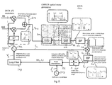
- Fig. 4 shows a bidirectional communication system 400.
- the bidirectioinal communication system comprises a home gateway 410 and a base station 420 arranged to communicate with each other.
- a data transfer from the home gateway 410 to the base station 420 or a user (not shown in Fig. 4 ) is done via a downlink 430.
- a data transfer from the base station 420 or a user to the base station 410 is done via an uplink 431.
- the home gateway 410 comprises a transmitter 411 similar to the radio communication system described above with a mode locked laser diode MLLD as carrier oscillator. Instead of the MLLD, the home gateway 410 can comprise any setup performing the same function as the MLLD, e.g., a combination of a laser and a modulator.
- the home gateway 410 further comprises a demodulator 412 to receive data via the uplink 431 and to demodulate this received data.
- the home gateway 410 can, e.g., be connected to an asymmetric digital subscriber line ADSL, a fibre to the home FTTH, and/or to cable TV.
- a power supply 413 is provided to power the home gateway 410.
- the base station 420 comprises a receiver 421 arranged to receive data from the optical downlink 430. Furthermore, the base station 420 comprises a transmitter 422 to send data via the optical uplink 431. A power supply 423 powers the base station 420. Further connection devices 424, 425, e.g. implemented as antennas, may be connected to the base station 420 for further data transfer to and from the base station 420.
- the bidirectional communication station 400 is adapted to transfer data through the downlink 430 in an optical signal comprising a carrier signal in the mmw-range, e.g. with a 60 GHz carrier.
- the signal to be transported is already in the desired frequency range so that the base station 420 can forward it via the connection device 424.
- the base station comprises a first filter for filtering a predetermined sideband signal from the data received via the downlink 430.
- the first filter of the base station is arranged immediately, meaning without electrical elements arranged in between, before the antenna connection device 424.
- the optical downlink 430 connection may comprise a fibre to transfer the data.
- the optical uplink 431 connection may also comprise a fiber for the data transfer. Furthermore, the optical uplink 431 may happen at lower frequencies, e.g. without the need of a millimetre wave carrier oscillator and a millimetre carrier frequency. Thus, a less expensive laser can be used in the base station 420 to transfer the data via the uplink 431, and not an expensive mmw-laser.
- lasers can not be modulated directly with mmw-signals. This is due to the material dynamics used for state of the art laser devices.
- mmw-signal e.g. combinations of lasers and external modulators or special laser diodes as mode-locked laser diodes are used to generate mmw-signals.
- the latter are not yet available commercially.
- combinations of lasers and external modulators have to be employed, the costs rise because of the increased complexity when using several devices.
- the received signal is converted or mixed down to an intermediate frequency IF.
- IF intermediate frequency
- commercial laser diodes e.g. DFB and VCSEL
- DFB and VCSEL can be modulated directly and are available in large quantities which in turn translates into lower system costs.
- 'Mixing down' and 'converting down' relates to a transformation to a lower frequency range.
- the base station 420 comprises a local oscillator LO BS .
- the signal of the local oscillator LO BS can be gained from signals received through the downlink 430 by use of a second filter of the base station.
- the second filter of the base station extracts the carrier signal from the signal received via the downlink 430 and transmits the carrier signal to means for mixing down an external signal for the uplink 431 as signal of the local oscillator LO BS .
- the number of hardware-components of the base station 420 is minimized.
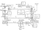
- Fig. 5 shows a bidirectional communication system 500.
- the bidirectional communication system 500 comprises the radio communication system 200 shown in Fig. 2 .
- the radio communication system 200 provides a signal for a downlink 530 to a base station 520.
- a fiber can be arranged to transfer the pre-mixed signal S PM provided by the radio communication system 200 via the downlink 530 to the base station 520.
- the pre-mixed signal S PM is received by an opto-electrical converter 526 of the base station 520.
- the pre-mixed signal S PM is in the mmw-range and comprises signals at the carrier frequency f C, ⁇ c and at the two sideband frequencies f C, ⁇ c - f 1, ⁇ 1 and f C, ⁇ c + f 1, ⁇ 1 enhanced with a phase error e( ⁇ c , ⁇ 1 ) of both the carrier oscillator 201 and the sub-carrier oscillator 202 and the bandwidth added from the modulator 212 carrying the information.
- At least one predetermined sideband of the pre-mixed signal S PM is stabilised as described in the description of Fig. 2 .
- the recieved pre-mixed signal S PM is divided and transferred to both a first bandpass filter 527 and to a second bandpass filter 528 of the base station 520.
- the first bandpass filter 527 of the base station 520 filters one sideband signal out of the premixed signal S PM which is centered at the frequency f C +f 1 .
- This filtered sideband signal is the predetermined mixing product stabilised by the radio communication system 200 and is transmitted by an antenna Tx.
- the second bandbass filter 528 of the base station 520 is arranged to filter the carrier signal S C from the pre-mixed signal S PM .
- This carrier signal S C is not stabilised, since the stabilisation of the phase locked loop of the radio communication system 200 is stabilising one or more of the mixing products, but not the carrier signal S C itself.
- This filtered carrier signal S C is used as local oscillator signal LO BS of the base station 520.
- an external sideband signal S E can be transmitted to the base station 520.
- the external sideband signal S E comprises a sideband signal centred at a frequency f C + f 1 that is stabilised externally, wherein this centre frequency comprises the same carrier frequency f C and the same sub-carrier frequency f 1 as used by the radio communication system 200.
- this external sideband signal S E , the sideband signal transmitted to the antenna Tx, and the predetermined sideband signal chosen for stabilisation by the phase locked loop of the radio communication system 200 are all at the same frequency, either the sum or the difference of the carrier frequency f C and the sub-carrier frequency f 1 .
- the external sideband signal S E is send to a conversion circuit 529 adapted to convert the external sideband signal S E down to its sub-carrier frequency range.
- the conversion circuit 529 performs the function of a down-converter, whereat the carrier signal S C provided by the second bandpass filter 528 is used as a local oscillator in the mixing process.
- the external sideband signal S E is thus down-converted and results in the external bandpass signal S BFE in the intermediate frequency range.
- the resulting external bandpass signal S BPE is at a frequency f 1, ⁇ c , enhanced by the phase error ⁇ c of the carrier oscillator 201 that is inherent in the carrier signal S C provided by the second band pass filter 528 of the base station 520.
- the conversion circuit 529 converts the external signal S E into a signal at the intermediate frequency (IF) f 1, ⁇ c, meaning at the sub-carrier frequency f 1 carrying the instability of the carrier signal S C .
- the external bandpass signal S BPE is used to modulate an electro-optical converter 532 like a laser which provides the signal for an uplink 531.
- the uplink 531 may be realised as an optical fibre.
- the external bandpass signal S BPE centred at the intermediate frequency f 1, ⁇ c is transmitted to a demodulator 512.
- the demodulator 512 is part of the home gateway 510 comprising the radio communication system 200 and the demodulator 512.
- the demodulator 512 is adapted to receive the external bandpass signal S BPE at the intermediate frequency f 1, ⁇ c from the uplink 531 by means of a opto-electrical converter 514.
- the demodulator 512 is further adapted to demodulate the external bandpass signal S BPE .
- the information in form of the corresponding I RX and Q RX symbols is retrieved by the demodulator 512 performing the inverse operation of modulator 212 and 312. Since the external bandpass signal S BPE was generated using the non-stabilised local oscillator signal LO BS of the base station 530, the instability of the carrier oscillator 201 is also found in the received baseband signal.
- the sub-carrier oscillator 202 of the radio communication system 200 is arranged to deliver its sub-carrier signal S C to at least three different circuit-parts of the bidirectional communication system: As described in connection with Fig. 2 , the sub-carrier signal S SC is sent to the modulator 212 to generate the information carrying and modulated sub-carrier signal S MSC . The sub-carrier signal S SC is also sent to the mixing means 203 to generate the mixed signal S M . Furthermore, the sub-carrier signal S SC is transmitted to the demodulator 512 and used by its demodulation circuit to demodulate the quadrature phase Q RX (t) and the inphase I RX (t) from the external bandpass signal S BPE and, thus, forming the baseband signal.
- the instability resulting from the carrier signal S C is compensated for in the baseband signal generated by the demodulator 512.
- Fig. 6 shows a bidirectional communication system 600 comprising a base station 620 and a home gateway 610.
- the home gateway 610 comprises the radio communication system 300 shown in Fig. 3 and a demodulator 612.
- the birectional communication system 600 is built similarly to the birectional communication system 500 shown in Fig. 5 .
- the bidirectional communication system 600 shown in Fig. 6 comprises an all electrical circuit.
- the pre-mixed signal S PM is generated at the mixing means 314 and sent via a downlink 630 to the base station 620. Via a first bandpass 627 of the base station 620, the predetermined sideband signal is filtered from the pre-mixed signal S PM and transmitted via antenna Tx out of the bidirectional communication system 600.
- a second bandpass filter 628 of the base station 620 is filtering the carrier signal S C from the pre-mixed signal S PM .
- This carrier signal S C forms a local oscillator signal LO BS of the bases station 620 and is used by converter means 629 to convert the external signal S E down into the external bandpass signal S BPE .
- the external bandpass signal S BPE is sent via an uplink 631 to the demodulator 610.
- the demodulator 610 is arranged to receive the sub-carrier signal S C from the radio communication system 300.
- the demodulator 610 uses the sub-carrier signal S C to demodulate the external bandpass signal S BPE in order to retrieve the baseband signal.
- the resulting baseband signal is stabilised.
- the bidirectional communication systems 400, 500, and 600 need only one expensive carrier oscillator 101, 201, 301 with millimetre wave capabilities to generate the carrier signal S C , e.g. in the mmw-range.
- the base station 420, 520, and 620 need no carrier oscillator, since the carrier signal S C of the radio communication system 100, 200, 300 is used to convert the external signal S E down to the external bandpass signal S BPE .
- the radio communication systems described above can operate in the band from 57-66 GHz where an over-all bandwidth of 9 GHz is available for license-free communication in Europe, Europe being the region that restricts the least. Therefore, in this particular example for European communication systems and under the actual license conditions (in the year 2011), the transmission sideband mustremain within this band for license-free communication in Europe. Therefore, for a carrier frequency f C of about 60 GHz, the sub-carrier frequency can, e.g., be allocated between 1 and 6 GHz, in particular between 1 and 3 GHz, Depending on the radio standard, different channels that can be occupied by the transmission sideband can be used. Examples for the allocated channels can be found in:
- the standards denote the centre frequencies of the bands (f C + f 1 or f C - f 1 ) used for transmission.
- the carrier frequencies should be chosen according to the designated band centre frequency and the chosen bandwidth.
- IEEE 802.15c or ECMA 387 channel 1 has a bandwidth of 2.61 GHz with a centre frequency of 58.320 GHz, the outer band limits being 57.240 GHz and 59.400 GHz.
- the respective standard transmit mask has to be respected, thus providing a (lower) limit for the sub-carrier frequency with respect to the chosen carrier.
- Spectral masks can be found in the standards:
Landscapes
- Engineering & Computer Science (AREA)
- Computer Networks & Wireless Communication (AREA)
- Signal Processing (AREA)
- Stabilization Of Oscillater, Synchronisation, Frequency Synthesizers (AREA)
Abstract
Description
- The invention relates to a radio communication system, a home gateway, a bidirectional communication system, and a method for stabilising a sideband signal.
- In the transmitter of a radio communication system, an information carrying digital sideband signal is modulated to an analogue sub-carrier signal. It is subsequently up-converted by being mixed with a radio frequency (RF) carrier in a dedicated frequency band corresponding to the target application. Through a basic mixing process, two sidebands are created around a spectral component corresponding to a carrier signal, one of which will be selected and transmitted by an antenna.
- A stable operation of the radio system can only be assured if the users can synchronise their receiver equipment with the central frequency of the transmitted sideband. The stability of this sideband is therefore essential for the overall function of the system. In conventional radio systems, certain measures are usually undertaken to stabilise the RF carrier, thus obtaining a stable sideband through the mixing process. That is why in conventional systems, the output frequency of a voltage controlled local oscillator (VC(L)O) serving as RF source is usually stabilised by using a phase locked loop (PLL) before up-converting the sub-carrier signal.
- By means of the phase locked loop a carrier phase noise can be reduced considerably. This method can always be applied as long as the local oscillator frequency is generated in such a way that it can be influenced by an electrical quantity, e.g. by a DC control voltage, so that small deviations from the nominal value can be compensated for by the phase locked loop. This is the case when conventional voltage controlled oscillators (VCO) are used as local oscillators (LO). The phase locked loop concept allows for the stabilisation of the single tone signal, such as the one at the output of a voltage controlled oscillator. It does not allow for the stabilisation of a signal that consists of several frequencies, like a modulated sideband signal.
- Techniques for the optical generation and transmission of RF signals in the millimetre wave-range are currently being investigated. These techniques represent a low cost alternative to electrical RF oscillators in future broad band communication systems in the 60 GHz range, for example for high data-rate home networks. They allow the nearly loss-free transmission of a millimetre wave signal over optical fibre networks to an antenna access point. In case of optical generation of the RF signal, the modulation and mixing process will be realised in the optical domain using intensity modulation (IM) as result of an electro-optical conversion and optical mixing. After a transmission of the optical signal across a fibre, the signal is detected by a suitable photodetector and converted back to an electrical signal (opto-electrical conversion). The RF carrier signal can be generated by interference (beating) of two monochromatic optical fields with a constant phase relation. In the photodetector, the interference results in an electrical current signal at an RF beat frequency corresponding to the separation in wavelength of the optical fields, thus providing an electrical RF carrier signal. Classic optical modulation methods are e.g. a direct modulation of the laser bias current or external modulation in dedicated modulators, e.g. lithium-niobate modulators.
- Thus, the stability of the RF carrier signal depends directly on the stability of the beat signal of the optical signals. Depending on the type of optical RF generation, this stability might not be influenceable in the same way as the voltage controlled oscillator that was described above. In the case that the beat signal shows an increased noise, this noise will also appear in the electrical signal derived therefrom. In the up-conversion process, this instability will be reproduced and be present in the sidebands. If such a sideband is then transmitted across a radio link, a synchronisation of the radio receiver will be hindered or even made impossible.
- In conventional analogue optical communication systems, optical or hybrid phase locked loops have already been proposed for the stabilisation of a monochromatic optical signal. These loops are based on the same principle as the conventional phase locked loop and have been, where necessary, completed by additional opto-electrical components. An electrical quantity or another accessible physical quantity serves as control variable for fine tuning of the optical oscillator as carrier oscillator. Consequently, the phase locked loop architecture has to be adapted according to the type of electro-optical converter, e.g. different laser architectures, or laser and modulator.
- Certain laser architectures allow for active mode locking of the optical modes. In this case, the modes can be stabilised by applying an electrical radio frequency signal of the same frequency as the desired carrier to the laser. The use of electrical radio frequency carriers is an expensive way to provide a stabilised sideband signal.
- Furthermore, optical feedback loops have been proposed, where a part of the laser light is reinjected into the cavity in a controlled manner. However, the set up is relatively complex, as the phase difference caused by the feed back loop has to be chosen exactly so as to match the optical phases of the signals leaving and reentering the cavity.
- In the most disadvantageous case, the phase of the optical signal cannot be fine tuned by an electrical signal. This might occur when the laser phase noise depends predominantly on its physical structure instead of on its bias circuitry, or when other optical components with increased noise contribution (e.g. optical amplifiers) are present in the optical subsystem.
- It is an object of the invention to provide improved means for generating a stabilised sideband signal.
- This object is achieved by the subject matter of the independent claims.
- According to an aspect, a radio communication system comprises a carrier oscillator that is configured to generate a carrier signal at a carrier frequency, a sub-carrier oscillator configured to generate a sub-carrier signal at a sub-carrier frequency, and a phase error detection means configured to generate an error indicator, in particular an error voltage, corresponding to a phase error of the carrier signal and/or the sub-carrier signal. The sub-carrier oscillator is implemented as a controlled oscillator, in particular a voltage controlled oscillator (VCO), being controlled by the error indicator of the phase error detection means. The phase error detection means is detecting the phase error of the carrier oscillator and/or the phase error of a mixed signal comprising mixing products of the carrier oscillator and the sub-carrier oscillator. The phase error can be caused by noise of the carrier oscillator and/or by noise of the sub-carrier oscillator. The detected phase error is not used to control the phase of the carrier oscillator as in conventional systems, but of the sub-carrier oscillator. Since the signal to be transmitted is a mixing product of the signal of the carrier oscillator and the sub-carrier oscillator, controlling the sub-carrier oscillator by variation of its DC control voltage and/or current derived from the detected phase error results in a stabilisation of the mixing product itself.
- One important signal to be generated by the radio communication system is a double sideband signal which consists of a carrier signal, e.g. in the millimetre wave range around 60 GHz, and of an upper and lower sideband of well defined bandwidth, representing the information to be transmitted. The double sideband signal is obtained by mixing the high frequency carrier signal with an information-carrying sub-carrier signal previously modulated by an information-carrying baseband signal.
- Thus, the sideband signals correspond to the mixing products and are centred at the frequency sum and frequency difference of the carrier frequency and the sub-carrier frequency. After one mixing product, meaning one of the sideband signals, has been chosen for transmission, an error indicator corresponding to the detected phase error is added to or subtracted from the control voltage and/or current of the sub-carrier oscillator in order to generate the stabilised sideband signal such that the centre frequencies of the two sidebands correspond to their nominal values.
- A mixing signal resulting from the mixing of two or more signals can comprise multiple spectral components referred to as mixing products at multiple frequencies, in particular at the sum and the difference of the frequencies of the original signals. The mixing product can further comprise parts of the original signals at their original frequencies.
- In such a radio communication system a carrier oscillator can be used that does not need to be voltage controlled, since its phase error and noise is compensated for by the voltage controlled sub-carrier oscillator.
- The sub-carrier oscillator is thus controlled by the phase error detection means, such that at least one of the mixing products of the carrier signaland the sub-carrier signal is stabilised through a reduction of the over-all phase error.
- The error indicator corresponding to the phase error means that the error indicator is a function of the detected phase error. The error indicator can e.g., be the control voltage for the sub-carrier oscillator enhanced by a voltage corresponding to the phase error, or it can e.g., be a voltage containing only the phase error that is added to or subtracted from the regular control voltage of the sub-carrier oscillator to compensate for the phase error of the carrier oscillator.
- A mixing process does not substantially change the phase noise characteristics of the signals to be mixed. Therefore, the instability of the carrier oscillator is transferred to another frequency range.
- Thus, an all electrical compensation of the phase error is provided, even if the carrier oscillator is implemented as an optical oscillator, such as a laser.
- The sub-carrier oscillator being implemented as a controlled oscillator means that its oscillating frequency can be adjusted according to one or more electrical parameters such as its drive voltage and/or drive current.
- A radio communication system is a system, in particular an analogue system, for generating a radio signal, in particular a sideband signal, in any electromagnetic or electric form.
- In one embodiment of the invention, the radio communication system comprises mixing means configured to generate a mixed signal comprising the carrier signal, the phase error, and the mixing products of the carrier signal and the sub-carrier signal. In this embodiment, the phase error detection means is configured to generate the error indicator from the mixed signal. The phase error of the sub-carrier oscillator is usually considerably lower than the phase error of the carrier oscillator. Therefore, the main detected phase error will be the phase error of the carrier oscillator. However, by including the phase error of the sub-carrier into the error indicator, at least one of the mixing products of the carrier signal and the sub-carrier signal is stabilised. Calculating the phase error from the mixed signal also comprises an assembly advantage that will become apparent below when the embodiments are discussed. The mixed signal from which the phase error is detected is implemented as a single tone signal. That means that it is implemented free of information modulation.
- In this embodiment, the radio communication system can comprise a pre-mixing means configured to generate a pre-mixed signal consisting of the carrier signal, the phase error, and the mixing products of the carrier and the sub-carrier signals. A band pass filter can be arranged to filter or extract the carrier signal out of the premixed signal. This pre-mixed signal can already comprise the sub-carrier signal, the sub-carrier signal comprising an information signal modulated therewith. Thus, extracting the carrier signal from this pre-mixed signal eliminates other spectral components induced by the mixing of the carrier signal with the information modulated sub-carrier signal from the resulting radio spectrum. Therein, the mixing means is arranged to generate the mixed signal using the carrier signal that is extracted from the pre-mixed signal. Thus, the mixing means generates a single tone mixed signal, from which the phase error is detected by the phase error detection means.
- The spectral components of the mixed signal appear at frequencies that correspond to combinations of the carrier frequency, the sub-carrier frequency, and the time derivative of the phase error.
- The spectral components of the pre-mixed signal appear at frequencies that correspond to combinations of the carrier frequency, the sub-carrier frequency and all frequencies within the spectrum resulting from an information signal modulated thereto, and the time derivative of the phase error.
- In one embodiment, the phase error detection means is implemented as a phase locked loop (PLL). The working principle of a phase locked loop is known to a person skilled in the art. Summarising, a phase locked loop generates an error indicator that corresponds, e.g. is proportional, to a phase error that is detected by comparing the frequency of a signal to be checked with a reference signal. The error indicator is a function of the phase error. The generated error indicator is used to control the sub-carrier oscillator so that the phase error in the up-converted mixed signal is minimised or eliminated.
- In one embodiment, the radio communication system comprises a modulator that is arranged to modulate an information signal to the sub-carrier signal. The sub-carrier oscillator thus provides a sub-carrier signal to the modulator that modulates the information signal to it, and e.g., by means of a second output, the sub-carrier oscillator can also provide its unmodulated signal to the mixing means that mixes the unmodulated sub-carrier signal with the carrier signal of the carrier oscillator. The information signal can comprise a time dependent inphase and quadrature component (I(t) and Q(t)). When it comprises such a modulator, the radio communication system can be used to transmit information in a stabilised sideband.
- In one embodiment, the carrier oscillator is implemented as an optical oscillator, e.g. as a laser. The frequency of most lasers cannot be modulated by changing a voltage. Therefore, sufficiently stable lasers are not used in conventional radio communication systems as described in the background of the invention. By stabilising the sub-carrier oscillators with the phase error of the carrier oscillator, lasers can be used as carrier oscillators even though the laser itself is not a voltage controlled oscillator and without the need of optical/hybrid phase locked loops. Generally speaking, the radio communication system is independent of the type of optical generation used.
- In one embodiment, the radio communication system comprises a transmitter to transmit a modulated sideband signal comprising the sub-carrier signal controlled by the error indicator of the phase error detection means. The transmitter can, for example, be an antenna to launch the signal into a wireless channel when the signal shall be transmitted as an electromagnetic wave, or a device to launch the signal into an optical fibre when the signal shall be transmitted as an optical wave. Alternatively, the signal can also be transmitted by a conventional wire connection as an electrical signal.
- The carrier oscillator can be implemented as a millimetre-wave(mmw-) oscillator, e.g. in the 60 GHz range. The sub-carrier frequency is usually considerably lower than the carrier frequency. Typical sub-carrier frequencies have a nominal value of about 1% to 20% of the carrier frequency.
- In one embodiment, the carrier oscillator is implemented as a free-running oscillator comprising a fixed control voltage. In other words, the carrier oscillator is not implemented as a voltage controlled oscillator of which the frequency can be influenced by regulating its control voltage/current.
- In one embodiment, the radio communication system comprises a band pass filter arranged to filter a predetermined mixing product from the spectrum of the mixed signal comprising the carrier signal and multiple mixing products of the carrier and the sub-carrier signals. This predetermined mixing product is selected to get stabilised and to transmit an information signal. The predetermined mixing product can, e.g. be a sideband signal at the frequency sum of the carrier frequency and the sub-carrier frequency. The predetermined signal can, e.g. be the signal at the frequency difference of the carrier frequency and the sub-carrier frequency. The band pass filter is thus used to extract the predetermined mixing product as selected spectral component further used by the radio communication system. The predetermined mixing product may also comprise the phase error.
- In one embodiment, the radio communication system comprises a reference oscillator arranged to provide a reference frequency to the phase error detection means. The reference oscillator can provide a fixed frequency, with which the frequency of the predetermined mixing product is compared to detect the phase error. The reference oscillator can, for example, be a quartz oscillator.
- The sub-carrier oscillator can be configured to oscillate at a sub-carrier frequency being substantially lower than the carrier frequency of the carrier oscillator. The sub-carrier frequency has a value of 1% to 20% of the carrier frequency, in particular, 5% to 10% of the carrier frequency.
- An aspect of the invention relates to a home gateway comprising a radio communication system as described above. The home gateway further comprises a demodulator adapted to demodulate an external bandpass signal using the sub-carrier signal provided by the sub-carrier oscillator of the radio communication system. The external bandpass signal may be provided by an uplink. In particular, the external bandpass signal may comprise a phase error of the carrier oscillator of the radio communication system. The external bandpass signal may be demodulated by a demodulator into a baseband signal. Thus, by using the sub-carrier signal provided by the sub-carrier oscillator of the radio communication system, the phase error of the carrier oscillator may be reduced or even eliminated in the baseband signal.
- An aspect of the invention relates to a bidirectional communication system comprising a home gateway as described above. The bidirectional communication system comprises a base station, wherein a downlink is adapted to transmit a signal from the radio communication system to the base station. An uplink is adapted to transmit the external bandpass signal from the base station to the demodulator. In particular, the signal to be transfered to the base station via the downlink may be the pre-mixed signal as described above. Furthermore, the base station may be adapted to extract the carrier signal from the signal received via the downlink and use this extracted carrier signal as local oscillator signal for converting an external signal down to the external bandpass signal. Thus, the external bandpass signal may comprise an instability of the carrier oscillator which may be eliminated in the baseband signal by the demodulator of the home gateway.
- An aspect of the invention relates to a method comprising the steps: Generating a carrier signal, generating a sub-carrier signal by means of a sub-carrier oscillator, mixing the carrier signal with the sub-carrier signal to form a mixed signal, detecting a phase error of the mixed signal, using the detected phase error to stabilise the sub-carrier oscillator, and generating a stabilised double sideband signal comprising the carrier signal and the stabilised sidebands, e.g. the mixing products of the sub-carrier signal and the carrier signal. In particular, at least the one of the mixing products selected as predetermined mixing product is filtered. The phase error of this predetermined mixing product is detected. Therefore, the method can comprise a step of filtering the predetermined mixing product, e.g. by means of a band-pass filter.
- The method can further comprise steps of using a single component or multiple components as described above.
- In an embodiment, the method further comprises the steps: receiving an external bandpass signal and demodulating the external bandpass signal using the sub-carrier signal of the sub-carrier oscillator.
- The method according to claim 13 can be applied to a radio communication system according to
claims 1 to 10. - The method according to claim 14 can be applied to a home gateway according to claim 11.
- An aspect of the invention relates to a computer program product for controlling a radio communication system according to any of the
claims 1 to 10 according to the method of claim 13. - An aspect of the invention relates to a computer program product for controlling a home gateway according to claim 11 according to the method of claim 14.
- The invention is further described by embodiments shown in the figures. In particular, it is shown by
- Fig. 1
- a radio communication system comprising a carrier oscillator and a sub-carrier oscillator;
- Fig. 2
- a radio communication system wherein the carrier oscillator is implemented as an optical generator;
- Fig. 3
- a radio communication system comprising an electrical carrier oscillator and an electrical sub-carrier oscillator;
- Fig. 4
- a bidirectional communication system;
- Fig. 5
- the radio communication system of
Fig. 2 , arranged in a biderectional communication system; and - Fig. 6
- the radio communication system of
Fig. 3 , arranged in a biderectional communication system. -
Fig. 1 schematically shows aradio communication system 100, in a simplified way, as an entirely electrical circuit. Theradio communication system 100 comprises a carrier oscillator 101 that generates a carrier signal SC and asub-carrier oscillator 102 that generates a sub-carrier signal SSC. The carrier signal SC is provided at a carrier frequency fC and can be enhanced by a carrier phase error εC. The sub-carrier signal SSC is provided at a sub-carrier frequency f1 which is considerably lower than the carrier frequency fC. The sub-carrier signal SSC can be enhanced by a sub-carrier phase error ε1. - The carrier signal SC and the sub-carrier signal SSC are mixed at mixing means 103. The mixing means 103 can, for example, be a multiplier that generates a mixed signal SM comprising mixing products of the carrier signal SC and the sub-carrier signal SSC. The mixed signal SM comprises signals at the following frequencies: fC,εc - f1,ε1, fC,εc, and fC,εc + f1,ε1. The signals at the two frequencies fC,εc - f1,ε1 and at fC,εc + f1,ε1 form two sideband signals. In other words, the mixed signal SM comprises the carrier signal SC at the carrier frequency fC enhanced by the phase error εC and two sideband signals, each sideband signal enhanced by a phase error e(εC,ε1) which is a function of both the carrier phase error εC and the sub-carrier phase error ε1.
- The mixed signal SM is then led to a first
band pass filter 104 that filters one sideband out of the mixed signal SM to form a single-tone signal. In most radio systems comprising a radio communication system used as a transmitter and a receiver, only one sideband is used for fine tuning both the transmitter and the receiver. Even if both sidebands are transmitted together with the carrier signal Sc, usually only one of the two sidebands is selected for the transmission and the reception of the information signal. This selected sideband is a predetermined or selected mixing product which is chosen from the multiple mixing products of the mixed signal SM for the stabilising procedure and the transmission of the information. - The first
band pass filter 104 centres around a frequency that equals to the centre frequency of one of the two sidebands. In one embodiment, the upper sideband at the frequency fc,εc + f1,ε1 is filtered from the mixed signal SM to form a single tone signal SST. In an alternative embodiment, theband pass filter 104 is configured to filter the lower sideband at fC,εc - f1,ε1. - The single tone signal SST is fed into a
divider 105. Thedivider 105 comprises a divider component to scale down the frequency of the single tone signal SST to a manageable frequency. The phase of the signal is then compared at aphase discriminator 106 to the phase of astable reference oscillator 107. Thereference oscillator 107 can, for example, be implemented as a crystal oscillator oscillating at a reference frequency fR. Thephase discriminator 106 outputs the phase error e(εC,ε1) of the single tone signal SST. - The phase error e(εC,ε1) of the single tone signal SST corresponds to a frequency error of its frequency, its deviation from the nominal frequency value. The frequency error of the provided carrier frequency fC from its intended frequency can, for example, be caused by noise and/or by a structurally faulty component of the carrier oscillator and/or by interference/resonance.
- The phase error e(εC,ε1) is converted into an error voltage signal Vε as an error indicator by a
loop filter 108. Theloop filter 108 integrates the phase error e(εC,ε1) and generates a control voltage for thesub-carrier oscillator 102 that comprises the error voltage Vε. - The components described above can be connected electrically, e.g. by wires, to enable a transmission of the different signals between the components.
- In the embodiment shown in
Fig. 1 , a stabilisation of the mixed signal SM is accomplished for two sinusoidal local oscillator signals delivered by the carrier oscillator 101 and thesub-carrier oscillator 102. The sub-carrier oscillator is a voltage controlled oscillator (VCO). The carrier oscillator 101 can be a free running oscillator that cannot be influenced in its phase, e.g. its control voltage cannot influence the carrier frequency fC. The output signal of the carrier oscillator 101 can comprise increased phase noise. - The
sub-carrier oscillator 102 is controlled by the phase locked loop that comprises thephase discriminator 106, thereference oscillator 107, and theloop filter 108. The mixed signal SM of bothoscillators 101 and 102 is filtered at the sum frequency fC,εc + f1,ε1, the upper sideband signal, and stabilised at a nominal value by controlling the sub-carrier frequency f1. Thus, this upper sideband signal is chosen as predetermined mixing product from the multiple mixing products of the mixing signal SM. -
Fig. 2 shows aradio communication system 200 that operates in parts similar to theradio communication system 100 shown inFig. 1 . Theradio communication system 200 comprises asub-carrier oscillator 202 delivering a sub-carrier signal SSC at the sub-carrier frequency f1. - A complex base band information signal can be described by its time-dependent inphase and quadrature component. A
modulator 212 modulates such an in-phase I(t) and such a quadrature phase Q(t) to the signal of the sub-carrier SSC to form a modulated sub-carrier signal SMSC. The modulated sub-carrier signal SMSC comprises a bandwidth around the sub-carrier frequency f1 and can carry complex base band information, thereby forming an information signal. The modulated sub-carrier signal SMSC forms a band pass signal. Themodulator 212 comprises a 90° phase shifter, a multiplier for mixing the in-phase I(t) to a part of the sub-carrier signal SSC, another multiplier for mixing the quadrature phase Q(t) to a part of the sub-carrier signal SSC shifted by 90° by the phase shifter, and an adder that adds both modulated parts of the sub-carrier signal SSC resulting in the modulated sub-carrier signal SMSC. - The modulated sub-carrier signal SMSC is fed into an electro-
optical converter 201. The electro-optical converter 201 is modulated by the modulated sub-carrier signal SMSC. At the conversion process from an electrical signal to an optical signal an optical up-conversion, e.g. mixing, into the millimetre wave range happens. The carrier frequency fC including a carrier phase error εC is chosen to be in the millimetre wave range. Thus, a pre-mixed signal SPM is generated. The pre-mixed signal SPM can be transmitted over a fibre link carried by the optical wave. The signal is received by an opto-electrical converter 210 which converts the optical signal back into an electrical signal. The electrical signal still contains the pre-mixed signal SPM comprising the carrier frequency fC,εc and the two sidebands fC,εc - f1,ε1 and fC,εc + f1,ε1, enhanced with a phase error e(εC,ε1) of both thecarrier oscillator 201 and thesubcarrier oscillator 202 and the bandwidth added from themodulator 212 carrying the information. - The pre-mixed signal SPM passes a second band pass filter 211 that filters only the signal component at the carrier frequency fC,εc enhanced by the carrier phase error ec out of the pre-mixed signal SPM. The second band pass filter 211 thus generates the carrier signal SC without the mixing products of the carrier signal SC and the modulated sub-carrier signal SSC present in the pre-mixed signal SPM. Further components of the
radio communication system 200 work similarly to the components of theradio communication system 100 shown inFig. 1 . - In particular, the
radio communication system 200 further comprises mixing means 203 to mix the carrier signal SC with the sub-carrier signal SSC in order to generate the mixed signal SM, a firstband pass filter 204 for generating the single tone signal SST, adivider 205, aphase discriminator 206, areference oscillator 207, and aloop filter 208 that generates the error voltage Vε, to stabilise thesub-carrier oscillator 202. - The signal component at the carrier oscillator frequency fC,εc is thus electrically filtered from an optically pre-mixed signal SPM, and the phase error e(εcC,ε1) of the single tone signal SST is detected by the phase error detection means to control the voltage controlled
sub-carrier oscillator 202. The pre-mixed signal SPM is not used to detect the phase error, because a single tone signal can not directly be extracted from its spectrum, as it exhibits a certain band-width depending on the information it is carrying. Therefore, the total phase error of the spectral component at a centre frequency fC,εc + f1,ε1 or fC,εc - f1,ε1 in the spectrum of the mixed signal SM is detected. By controlling the sub-carrier frequency f1 through the feedback of the detected phase error e(εC,ε1), and using the carrier signal SC to generate the pre-mixed signal SPM, the sideband in the spectrum of SPM can always be placed at the correct frequency despite the inherent instability of the carrier signal Sc. A mixing process does not substantially change the phase noise characteristics of the signals to be mixed. Therefore, the instability of the carrier oscillator is transferred to another frequency range. - The pre-mixed signal SPM can be transmitted by a transmitter such that it comprises a stabilised sideband. It is the pre-mixed signal SPM that is supposed to be sent across a transmission channel. The filtering of the pre-mixed signal SPM, and mixing the filtered carrier signal SC anew with the sub-carrier signal SSC, effectively removes its bandwidth. Thus, the phase error e(εC,ε1) can be detected in the mixed signal SM comprising only single-tone spectral components.
- The
radio communication system 200 further comprises a transmitter 209 that transmits the optical pre-mixed signal SPM that was generated by the electro-optical converter 201. Alternatively, theradio communication system 200 can also transmit the pre-mixed signal SPM in electrical form after it was converted back into an electrical signal by the opto-electrical converter 210. -
Fig. 3 shows aradio communication system 300 which is built similarly to theradio communication system 200 shown inFig. 2 . In contrast with theradio communication system 200 shown inFig. 2 , theradio communication system 300 shown inFig. 3 comprises an all electrical circuit. - The
radio communication system 300 comprises asub-carrier oscillator 302 that generates a sub-carrier signal SSC at a sub-carrier frequency f1. The sub-carrier signal SSC is modulated by amodulator 312 adding information and generating a modulated sub-carrier signal SMSC. The modulated sub-carrier signal SMSC is mixed with the carrier signal SC provided by acarrier oscillator 301 at mixing means 314 to generate a pre-mixed signal SPM. The pre-mixed signal SPM is filtered by a secondband pass filter 311 so that only the carrier signal SC comprising the phase error ε remains. Mixing means 303 mixes the extracted carrier signal Sc with the sub-carrier signal SSC to form a mixed signal SM. - The mixed signal SM is filtered by a first
band pass filter 304 filtering only a single side band to generate the single tone signal SST. Adivider 305, a reference oscillator 307, aphase discriminator 306 and theloop filter 308 form phase error detection means that detects the phase error ε and generates the phase error voltage Vε that stabilises thesub-carrier oscillator 302. - The
radio communication system 300 comprises atransmitter 309 that outputs the pre-mixed signal SPM containing the carrier signal Sc at the carrier frequency fc and two sidebands carrying information that was modulated to the stabilised sub-carrier signal SSC by themodulator 312. Thus, thetransmitter 309 transmits a signal comprising a stabilised sideband. - In the embodiments shown in
Figs. 1 to 3 , the phase error detection means are provided by thereference oscillators phase discriminators sub-carrier oscillators modulators sub-carrier oscillators - The two sidebands at the frequency fC,εc - f1,ε1 and fC,εc + f1,ε1 are provided as symmetrical sidebands corresponding to the amplitude modulation (AM), or where applicable, intensity modulation (IM) at the modulation frequency f1. Mixing the sub-carrier signal SSC with the carrier signal SC that was extracted by the second band pass filter recreates the spectrum at the sidebands without the bandwidth resulting from the modulator. The single tone signal SST corresponds to the sub-carrier signal, up-converted to the millimetre wave range and enhanced by the phase error of both the carrier frequency fC and the sub-carrier frequency f1. The phase error of the single tone signal SST is compensated for by a phase locked loop as phase error detection means.
- In the embodiments shown in the figures, the
radio communication systems figures 4 to 6 ) to receive the stabilised sideband signal. - The embodiments shown in
figures 1 to 3 show the radio communication system and its components and also illustrate the method of how to control and drive this radio communication system to provide a stabilised sideband signal. - The invention enables the stabilisation of a predetermined mixing product centred at the sum and/or difference frequency of two oscillators, wherein only one of the two oscillators needs to be controllable. In particular, the invention enables the stabilisation of an optically generated sideband in the millimetre wave range, independently from the type of optical radio frequency generation (different laser architecture, or laser and modulator). In case of electro-optical converters whose architecture does not allow control of the frequency generating oscillator, the invention enables the stabilisation required for the error-free operation of the radio communication system. In particular, the invention enables the use of low cost, easy to integrate laser architectures, such as the mode locked semiconductor laser for millimetre wave generation described in the following example.
- One example of a laser architecture as a carrier oscillator is a passively mode-locked semiconductor laser without saturable absorber section. It exhibits a broad comb spectrum with inherent phase-lock of all optical modes under DC supply conditions only. The physical dimension of the laser cavity determines the different frequencies of the modes and, thus, the beat frequencies of the incident light on a photo-detector. The photo-detector is limited in bandwidth and acts like a low-pass. Thus, the photo-detector filters only the interference corresponding to the lowest frequency. This corresponds to the superposition of the interferences produced by each pair of neighbouring modes. Thus, the phase noise of the superposed modes determines the phase noise of the electrical RF carrier signal Sc. As the laser is operated under DC supply only, the spectral purity of the optical modes cannot be influenced by a conventional control loop. However, it can be used, for example, as
carrier oscillator 201 of theradio communication system 200 shown inFig. 2 . -
Fig. 4 shows abidirectional communication system 400. The bidirectioinal communication system comprises a home gateway 410 and abase station 420 arranged to communicate with each other. A data transfer from the home gateway 410 to thebase station 420 or a user (not shown inFig. 4 ) is done via adownlink 430. A data transfer from thebase station 420 or a user to the base station 410 is done via anuplink 431. - The home gateway 410 comprises a
transmitter 411 similar to the radio communication system described above with a mode locked laser diode MLLD as carrier oscillator. Instead of the MLLD, the home gateway 410 can comprise any setup performing the same function as the MLLD, e.g., a combination of a laser and a modulator. The home gateway 410 further comprises ademodulator 412 to receive data via theuplink 431 and to demodulate this received data. The home gateway 410 can, e.g., be connected to an asymmetric digital subscriber line ADSL, a fibre to the home FTTH, and/or to cable TV. Apower supply 413 is provided to power the home gateway 410. - The
base station 420 comprises areceiver 421 arranged to receive data from theoptical downlink 430. Furthermore, thebase station 420 comprises atransmitter 422 to send data via theoptical uplink 431. Apower supply 423 powers thebase station 420.Further connection devices base station 420 for further data transfer to and from thebase station 420. - Preferably, the
bidirectional communication station 400 is adapted to transfer data through thedownlink 430 in an optical signal comprising a carrier signal in the mmw-range, e.g. with a 60 GHz carrier. Thus, the signal to be transported is already in the desired frequency range so that thebase station 420 can forward it via theconnection device 424. The base station comprises a first filter for filtering a predetermined sideband signal from the data received via thedownlink 430. Therein, the first filter of the base station is arranged immediately, meaning without electrical elements arranged in between, before theantenna connection device 424. Theoptical downlink 430 connection may comprise a fibre to transfer the data. - The
optical uplink 431 connection may also comprise a fiber for the data transfer. Furthermore, theoptical uplink 431 may happen at lower frequencies, e.g. without the need of a millimetre wave carrier oscillator and a millimetre carrier frequency. Thus, a less expensive laser can be used in thebase station 420 to transfer the data via theuplink 431, and not an expensive mmw-laser. - At present, lasers can not be modulated directly with mmw-signals. This is due to the material dynamics used for state of the art laser devices. In order to generate a mmw-signal, e.g. combinations of lasers and external modulators or special laser diodes as mode-locked laser diodes are used to generate mmw-signals. The latter are not yet available commercially. In the event where combinations of lasers and external modulators have to be employed, the costs rise because of the increased complexity when using several devices.
- Within the
base station 420, the received signal is converted or mixed down to an intermediate frequency IF. In this IF range, commercial laser diodes, e.g. DFB and VCSEL, can be modulated directly and are available in large quantities which in turn translates into lower system costs. 'Mixing down' and 'converting down' relates to a transformation to a lower frequency range. To accomplish this down conversion, thebase station 420 comprises a local oscillator LOBS. The signal of the local oscillator LOBS can be gained from signals received through thedownlink 430 by use of a second filter of the base station. The second filter of the base station extracts the carrier signal from the signal received via thedownlink 430 and transmits the carrier signal to means for mixing down an external signal for theuplink 431 as signal of the local oscillator LOBS. Thus, the number of hardware-components of thebase station 420 is minimized. -
Fig. 5 shows abidirectional communication system 500. Thebidirectional communication system 500 comprises theradio communication system 200 shown inFig. 2 . Theradio communication system 200 provides a signal for adownlink 530 to abase station 520. A fiber can be arranged to transfer the pre-mixed signal SPM provided by theradio communication system 200 via thedownlink 530 to thebase station 520. - The pre-mixed signal SPM is received by an opto-electrical converter 526 of the
base station 520. The pre-mixed signal SPM is in the mmw-range and comprises signals at the carrier frequency fC,εc and at the two sideband frequencies fC,εc - f1,ε1 and fC,εc + f1,ε1 enhanced with a phase error e(εc,ε1) of both thecarrier oscillator 201 and thesub-carrier oscillator 202 and the bandwidth added from themodulator 212 carrying the information. At least one predetermined sideband of the pre-mixed signal SPM is stabilised as described in the description ofFig. 2 . - The recieved pre-mixed signal SPM is divided and transferred to both a
first bandpass filter 527 and to asecond bandpass filter 528 of thebase station 520. Thefirst bandpass filter 527 of thebase station 520 filters one sideband signal out of the premixed signal SPM which is centered at the frequency fC+f1. This filtered sideband signal is the predetermined mixing product stabilised by theradio communication system 200 and is transmitted by an antenna Tx. - The
second bandbass filter 528 of thebase station 520 is arranged to filter the carrier signal SC from the pre-mixed signal SPM. This carrier signal SC is not stabilised, since the stabilisation of the phase locked loop of theradio communication system 200 is stabilising one or more of the mixing products, but not the carrier signal SC itself. This filtered carrier signal SC is used as local oscillator signal LOBS of thebase station 520. - Via an antenna Rx an external sideband signal SE can be transmitted to the
base station 520. The external sideband signal SE comprises a sideband signal centred at a frequency fC + f1 that is stabilised externally, wherein this centre frequency comprises the same carrier frequency fC and the same sub-carrier frequency f1 as used by theradio communication system 200. In particular, this external sideband signal SE, the sideband signal transmitted to the antenna Tx, and the predetermined sideband signal chosen for stabilisation by the phase locked loop of theradio communication system 200 are all at the same frequency, either the sum or the difference of the carrier frequency fC and the sub-carrier frequency f1. - Together with the local oscillator signal LOBS of the
base station 520, the external sideband signal SE is send to aconversion circuit 529 adapted to convert the external sideband signal SE down to its sub-carrier frequency range. Theconversion circuit 529 performs the function of a down-converter, whereat the carrier signal SC provided by thesecond bandpass filter 528 is used as a local oscillator in the mixing process. The external sideband signal SE is thus down-converted and results in the external bandpass signal SBFE in the intermediate frequency range. The resulting external bandpass signal SBPE is at a frequency f1,εc, enhanced by the phase error εc of thecarrier oscillator 201 that is inherent in the carrier signal SC provided by the secondband pass filter 528 of thebase station 520. Thus, theconversion circuit 529 converts the external signal SE into a signal at the intermediate frequency (IF) f1,εc, meaning at the sub-carrier frequency f1 carrying the instability of the carrier signal SC. - The external bandpass signal SBPE is used to modulate an electro-
optical converter 532 like a laser which provides the signal for anuplink 531. Theuplink 531 may be realised as an optical fibre. - Thus, via the
uplink 531, the external bandpass signal SBPE centred at the intermediate frequency f1,εc is transmitted to a demodulator 512. - The demodulator 512 is part of the
home gateway 510 comprising theradio communication system 200 and the demodulator 512. - The demodulator 512 is adapted to receive the external bandpass signal SBPE at the intermediate frequency f1,εc from the
uplink 531 by means of a opto-electrical converter 514. The demodulator 512 is further adapted to demodulate the external bandpass signal SBPE. Thus, the information in form of the corresponding IRX and QRX symbols is retrieved by the demodulator 512 performing the inverse operation ofmodulator base station 530, the instability of thecarrier oscillator 201 is also found in the received baseband signal. - The
sub-carrier oscillator 202 of theradio communication system 200 is arranged to deliver its sub-carrier signal SC to at least three different circuit-parts of the bidirectional communication system: As described in connection withFig. 2 , the sub-carrier signal SSC is sent to themodulator 212 to generate the information carrying and modulated sub-carrier signal SMSC. The sub-carrier signal SSC is also sent to the mixing means 203 to generate the mixed signal SM. Furthermore, the sub-carrier signal SSC is transmitted to the demodulator 512 and used by its demodulation circuit to demodulate the quadrature phase QRX(t) and the inphase IRX(t) from the external bandpass signal SBPE and, thus, forming the baseband signal. - By using the subcarrier signal SSC generated by the
radio communication 200 implemented as stabilising unit to demodulate the external bandpass signal SBPE, the instability resulting from the carrier signal SC is compensated for in the baseband signal generated by the demodulator 512. -
Fig. 6 shows abidirectional communication system 600 comprising abase station 620 and ahome gateway 610. Thehome gateway 610 comprises theradio communication system 300 shown inFig. 3 and ademodulator 612. - The
birectional communication system 600 is built similarly to thebirectional communication system 500 shown inFig. 5 . In contrast with thebidirectional communication system 500 shown inFig. 5 , thebidirectional communication system 600 shown inFig. 6 comprises an all electrical circuit. - The pre-mixed signal SPM is generated at the mixing means 314 and sent via a
downlink 630 to thebase station 620. Via afirst bandpass 627 of thebase station 620, the predetermined sideband signal is filtered from the pre-mixed signal SPM and transmitted via antenna Tx out of thebidirectional communication system 600. - A
second bandpass filter 628 of thebase station 620 is filtering the carrier signal SC from the pre-mixed signal SPM. This carrier signal SC forms a local oscillator signal LOBS of thebases station 620 and is used by converter means 629 to convert the external signal SE down into the external bandpass signal SBPE. - The external bandpass signal SBPE is sent via an
uplink 631 to thedemodulator 610. Thedemodulator 610 is arranged to receive the sub-carrier signal SC from theradio communication system 300. Thedemodulator 610 uses the sub-carrier signal SC to demodulate the external bandpass signal SBPE in order to retrieve the baseband signal. By using the sub-carrier signal SC which is modified by the stabilising function of theradio communication system 300, the resulting baseband signal is stabilised. - The
bidirectional communication systems expensive carrier oscillator base station radio communication system carrier oscillator demodulator sub-carrier oscillator - As an example, the radio communication systems described above can operate in the band from 57-66 GHz where an over-all bandwidth of 9 GHz is available for license-free communication in Europe, Europe being the region that restricts the least. Therefore, in this particular example for European communication systems and under the actual license conditions (in the year 2011), the transmission sideband mustremain within this band for license-free communication in Europe. Therefore, for a carrier frequency fC of about 60 GHz, the sub-carrier frequency can, e.g., be allocated between 1 and 6 GHz, in particular between 1 and 3 GHz, Depending on the radio standard, different channels that can be occupied by the transmission sideband can be used. Examples for the allocated channels can be found in:
- IEEE 802.15c-2009: MAC and PHY Specification for High Rate Wireless Personal Area Networks,
page 60 - ECMA-387: High Rate 60GHz PHY, MAC and HDMI PAL, page 96
- The standards denote the centre frequencies of the bands (fC + f1 or fC - f1) used for transmission. The carrier frequencies should be chosen according to the designated band centre frequency and the chosen bandwidth. For example, IEEE 802.15c or ECMA 387
channel 1 has a bandwidth of 2.61 GHz with a centre frequency of 58.320 GHz, the outer band limits being 57.240 GHz and 59.400 GHz. Once the channel has been chosen, the respective standard transmit mask has to be respected, thus providing a (lower) limit for the sub-carrier frequency with respect to the chosen carrier. Spectral masks can be found in the standards: - IEEE 802.15c-2009: MAC and PHY Specification for High Rate Wireless Personal Area Networks, page 60 - 61
- ECMA-387: High Rate 60GHz PHY, MAC and HDMI PAL, page 98-99
-
- 100
- radio communication system
- 101
- carrier oscillator
- 102
- sub-carrier oscillator
- 103
- mixing means
- 104
- first band pass filter
- 105
- divider
- 106
- phase discriminator
- 107
- reference oscillator
- 108
- phase locked loop
- 200
- radio communication system
- 201
- carrier oscillator
- 202
- sub-carrier oscillator
- 203
- mixing means
- 204
- first band pass filter
- 205
- divider
- 206
- phase discriminator
- 207
- reference oscillator
- 208
- phase locked loop
- 209
- transmitter
- 210
- opto-electrical converter
- 211
- second band pass filter
- 212
- modulator
- 300
- radio communication system
- 301
- carrier oscillator
- 302
- sub-carrier oscillator
- 303
- mixing means
- 304
- first band pass filter
- 305
- divider
- 306
- phase discriminator
- 307
- reference oscillator
- 308
- phase locked loop
- 309
- transmitter
- 311
- second band pass filter
- 312
- modulator
- 314
- pre-mixing means
- 400
- bidirectional communication system
- 410
- home gateway
- 411
- transmitter
- 412
- demodulator
- 413
- power supply
- 420
- base station
- 421
- receiver
- 422
- transmitter
- 423
- power supply
- 430
- downlink
- 431
- uplink
- 424
- connection
- 425
- connection
- 500
- bidirectional communication system
- 510
- home gateway
- 512
- demodulator
- 514
- opto-electrical converter
- 520
- base station
- 526
- opto-electrical converter
- 527
- first bandpass filter of the base station
- 528
- second bandpass filter of the base station
- 529
- conversion circuit
- 530
- downlink
- 531
- uplink
- 532
- electric-optical converter
- 600
- bidirectional communication system
- 610
- home gateway
- 612
- demodulator
- 620
- base station
- 627
- first bandpass filter of the base station
- 628
- second bandpass filter of the base station
- 629
- conversion means
- 630
- downlink
- 631
- uplink
- f1
- sub-carrier frequency
- fC
- carrier frequency
- fR
- reference frequency
- εC
- carrier phase error
- ε1
- sub-carrier phase error
- e(εC, ε1)
- phase error
- Tx
- external sending antenna
- Rx
- external receiving antenna
- Vε
- error voltage
- SBPE
- external bandpass signal
- SC
- carrier signal
- SSC
- sub-carrier signal
- SE
- external sideband signal
- SMSC
- modulated sub-carrier signal
- SM
- mixed signal
- SPM
- pre-mixed signal
- SST
- single-tone signal
Claims (15)
- Radio communication system comprising- a carrier oscillator (101; 201; 301) configured to generate a carrier signal (SC) at a carrier frequency (fc),- a sub-carrier oscillator (102; 202; 302) configured to generate a sub-carrier signal (SSC) at a sub-carrier frequency (f1), and- a phase error detection means (106, 107, 108; 206, 207, 208; 306, 307, 308) configured to generate an error-indicator (Vε) corresponding to a phase error (e(εC,ε1))of a mixed signal (SM) comprising mixing products of the carrier signal (SC) and the sub-carrier signal (SSC), wherein
the sub-carrier oscillator (102; 202; 302) is implemented as a controlled-oscillator (102; 202; 302) being controlled by the error-indicator (Vε) of the phase error detection means (106, 107, 108; 206, 207, 208; 306, 307, 308). - System according to claim 1, wherein the sub-carrier oscillator (102; 202; 302) is stabilised by the phase error detection means (106, 107, 108; 206, 207, 208; 306, 307, 308).
- System according to claim 1 or 2, comprising mixing means (103; 203; 303) configured to generate the mixed signal (SM) enhanced by the phase error (e(εC,ε1)), the mixed signal (SM) comprising the carrier signal (SC), the phase error (e(εC,ε1)) and mixing products of the sub-carrier signal (SSC) and the carrier signal (SC), and wherein the phase error detection means (106, 107, 108; 206, 207, 208; 306, 307, 308) is configured to generate the error-indicator (Vε) based on the phase error (e(εC,ε1)) of the mixed signal (SM).
- System according to claim 3, comprising
a pre-mixing means (201; 314) configured to generate a pre-mixed signal (SPM) comprising the carrier signal (SC), the sub-carrier signal (SSC), and mixing products of the carrier signal (SC) and the sub-carrier signal (SSC),
the system further comprising a second band pass filter (211; 311) arranged to extract the carrier signal (SC) out of the pre-mixed signal (SPM), wherein the mixing means (103; 203; 303) is arranged to generate the mixed signal (SM) using the extracted carrier signal (SC). - System according to any of the preceding claims, wherein the phase error detection means (106, 107, 108; 206, 207, 208; 306, 307, 308) is implemented as and/or comprises a phase locked loop (108; 208; 308).
- System according to any of the preceding claims, comprising a modulator (212; 312) arranged to modulate an information signal to the sub-carrier signal (SMSC).
- System according to any of the preceding claims, comprising a transmitter (201; 309) to transmit a modulated sideband-signal comprising the sub-carrier signal (SSC) controlled by the error-indicator (Vε) of the phase error detection means (106, 107, 108; 206, 207, 208; 306, 307, 308).
- System according to any of the preceding claims, wherein the carrier oscillator (101; 201; 301) is implemented as an optical oscillator (201), and/or an mmw-oscillator, and/or as a free-running oscillator comprising a fixed control voltage or fixed drive current, wherein the carrier oscillator may be implemented as a laser,.
- System according to any of the preceding claims, comprising a first band pass filter (104; 204; 304) arranged to filter a predetermined mixing product from the spectrum of a mixed signal comprising the carrier signal and the mixing products of the carrier and the sub-carrier signals.
- System according to any of the preceding claims, comprising a reference oscillator (107; 207; 307) arranged to provide a reference frequency (fR) to the phase error detection means (106, 107, 108; 206, 207, 208; 306, 307, 308).
and/or
wherein the sub-carrier oscillator (102; 202; 302) is configured to oscillate at the sub-carrier frequency (f1), wherein the sub-carrier frequency (f1) is substantially lower than the carrier frequency (fC) of the carrier oscillator (101; 201; 301). - Home gateway comprising a radio communication system according to any of the preceding claims, comprising a demodulator (412; 512; 612) adapted to demodulate an external bandpass signal (SBPE) using the sub-carrier signal (SSC) provided by the sub-carrier oscillator (102; 202; 302) of the radio communication system (100; 200; 300).
- Bidirectional communication system comprising a home gateway according to claim 11, comprising a base station (420; 520; 620), wherein a downlink (431; 531; 631) is adapted to transmit a signal (SPM) from the radio communication system (100; 200; 300) to the base station (420; 520; 620), and wherein an uplink (431; 531; 631) is adapted to transmit the external bandpass signal (SBPE) from the base station (420; 520; 620) to the demodulator (412; 512; 612).
- Method for stabilising a sideband-signal, comprising the steps:- generating a carrier signal (SC),- generating a sub-carrier signal (SSC) by means of a sub-carrier oscillator (102; 202; 302),- detecting a phase error (e(εC,ε1)) of a mixed signal (SM) comprising a mixing products of the carrier signal (SC) and the sub-carriersignal (SSC),- using the detected phase error (e(εC, ε1)) to stabilise the sub-carrier oscillator (102; 202; 302) to generate a stabilised sub-carrier signal (SSC), and- generating a stabilised sideband-signal comprising the carrier signal (SC) and the stabilised sub-carrier signal (SSC).
- Method according to claim 13, further comprising the steps:- receiving an external bandpass signal (SBPE) and- demodulating the external bandpass signal (SBPE) using the sub-carrier signal (SSC).
- Applying the method according to claim 13 to a radio communication system (100; 200; 300) according to any of the claims 1 to 10, and/or applying the method according to claim 14 to a home gateway (410; 510; 610) according to claim 11.
Priority Applications (1)
| Application Number | Priority Date | Filing Date | Title |
|---|---|---|---|
| EP20110290482 EP2584749B1 (en) | 2011-10-19 | 2011-10-19 | Radio communication system, home gateway, bidirectional communication system, and method for stabilising a sideband signal |
Applications Claiming Priority (1)
| Application Number | Priority Date | Filing Date | Title |
|---|---|---|---|
| EP20110290482 EP2584749B1 (en) | 2011-10-19 | 2011-10-19 | Radio communication system, home gateway, bidirectional communication system, and method for stabilising a sideband signal |
Publications (2)
| Publication Number | Publication Date |
|---|---|
| EP2584749A1 true EP2584749A1 (en) | 2013-04-24 |
| EP2584749B1 EP2584749B1 (en) | 2014-09-10 |
Family
ID=44992814
Family Applications (1)
| Application Number | Title | Priority Date | Filing Date |
|---|---|---|---|
| EP20110290482 Not-in-force EP2584749B1 (en) | 2011-10-19 | 2011-10-19 | Radio communication system, home gateway, bidirectional communication system, and method for stabilising a sideband signal |
Country Status (1)
| Country | Link |
|---|---|
| EP (1) | EP2584749B1 (en) |
Cited By (2)
| Publication number | Priority date | Publication date | Assignee | Title |
|---|---|---|---|---|
| CN115189861A (en) * | 2022-07-06 | 2022-10-14 | 中国电子科技集团公司第五十四研究所 | A bidirectional one-way frequency synchronization method based on coherent frequency difference measurement |
| CN116346229A (en) * | 2023-04-17 | 2023-06-27 | 中国电子科技集团公司第五十四研究所 | A high-precision optical fiber radio frequency transmission system and calibration method |
Citations (5)
| Publication number | Priority date | Publication date | Assignee | Title |
|---|---|---|---|---|
| US4060773A (en) * | 1976-01-28 | 1977-11-29 | Tokyo Shibaura Electric Co., Ltd. | Frequency modulation system |
| US5940457A (en) * | 1996-02-06 | 1999-08-17 | State Of Israel-Ministry Of Defense Armament Development Authority-Rafael | Millimeter-wave (MMW) synthesizer with FSK modulation transmitter |
| US6255912B1 (en) * | 1999-09-27 | 2001-07-03 | Conexant Systems, Inc. | Phase lock loop used as up converter and for reducing phase noise of an output signal |
| US20060220750A1 (en) * | 2005-03-29 | 2006-10-05 | Renesas Technology Corp. | Phase locked loop circuits, offset PLL transmitters, radio frequency integrated circuits and mobile phone systems |
| WO2010094171A1 (en) * | 2009-02-17 | 2010-08-26 | Huawei Technologies Co., Ltd. | Method and apparatus for generating a carrier frequency signal |
-
2011
- 2011-10-19 EP EP20110290482 patent/EP2584749B1/en not_active Not-in-force
Patent Citations (5)
| Publication number | Priority date | Publication date | Assignee | Title |
|---|---|---|---|---|
| US4060773A (en) * | 1976-01-28 | 1977-11-29 | Tokyo Shibaura Electric Co., Ltd. | Frequency modulation system |
| US5940457A (en) * | 1996-02-06 | 1999-08-17 | State Of Israel-Ministry Of Defense Armament Development Authority-Rafael | Millimeter-wave (MMW) synthesizer with FSK modulation transmitter |
| US6255912B1 (en) * | 1999-09-27 | 2001-07-03 | Conexant Systems, Inc. | Phase lock loop used as up converter and for reducing phase noise of an output signal |
| US20060220750A1 (en) * | 2005-03-29 | 2006-10-05 | Renesas Technology Corp. | Phase locked loop circuits, offset PLL transmitters, radio frequency integrated circuits and mobile phone systems |
| WO2010094171A1 (en) * | 2009-02-17 | 2010-08-26 | Huawei Technologies Co., Ltd. | Method and apparatus for generating a carrier frequency signal |
Non-Patent Citations (3)
| Title |
|---|
| "PHASE-LOCKED LOOP", IBM TECHNICAL DISCLOSURE BULLETIN, INTERNATIONAL BUSINESS MACHINES CORP. (THORNWOOD), US, vol. 32, no. 6B, 1 November 1989 (1989-11-01), pages 465/466, XP000073847, ISSN: 0018-8689 * |
| ECMA-387: HIGH RATE 60GHZ PHY, MAC AND HDMI PAL, pages 96 |
| IEEE 802.15C-2009: MAC AND PHY SPECIFICATION FOR HIGH RATE WIRELESS PERSONAL AREA NETWORKS, pages 60 |
Cited By (3)
| Publication number | Priority date | Publication date | Assignee | Title |
|---|---|---|---|---|
| CN115189861A (en) * | 2022-07-06 | 2022-10-14 | 中国电子科技集团公司第五十四研究所 | A bidirectional one-way frequency synchronization method based on coherent frequency difference measurement |
| CN115189861B (en) * | 2022-07-06 | 2024-04-19 | 中国电子科技集团公司第五十四研究所 | A two-way one-way frequency synchronization method based on coherent frequency difference measurement |
| CN116346229A (en) * | 2023-04-17 | 2023-06-27 | 中国电子科技集团公司第五十四研究所 | A high-precision optical fiber radio frequency transmission system and calibration method |
Also Published As
| Publication number | Publication date |
|---|---|
| EP2584749B1 (en) | 2014-09-10 |
Similar Documents
| Publication | Publication Date | Title |
|---|---|---|
| KR100745749B1 (en) | Fiber-Radio Mixed Bidirectional Communication Device and Method | |
| US6963442B2 (en) | Low-noise, switchable RF-lightwave synthesizer | |
| EP2590343B1 (en) | Antenna synchronization for coherent network mimo | |
| US6366620B1 (en) | VSAT system | |
| CN103595477B (en) | Data-signal up-conversion method and apparatus | |
| US10116395B2 (en) | Photonic microwave mixing apparatus and method thereof | |
| CN106134108B (en) | Decode combined AM and FM signals | |
| Kaszubowska et al. | Multifunctional operation of a fiber Bragg grating in a WDM/SCM radio over fiber distribution system | |
| EP2188921B1 (en) | Electrically controlled optical oscillator for a single-side-subcarrier optical phase-locked loop | |
| US6922402B1 (en) | Mutual frequency locking across a link | |
| CN114039665A (en) | Multi-carrier frequency generation and reliable transmission method for RoF system | |
| EP2584749B1 (en) | Radio communication system, home gateway, bidirectional communication system, and method for stabilising a sideband signal | |
| Tian et al. | Experimental comparison of DSB-SC & OSSB based 60 GHz radio-over-fiber fronthaul links | |
| US8428464B2 (en) | Methods and devices for detection of a first signal superimposed on a second signal | |
| US20110091217A1 (en) | Apparatus and method for transporting multiple radio signals over optical fiber | |
| US10985842B2 (en) | Method for receiving a modulated optical signal and receiver unit | |
| US20080292326A1 (en) | Optical Voltage Controlled Oscillator for an Optical Phase Locked Loop | |
| JP4164570B2 (en) | Wireless optical fusion communication system and wireless optical fusion communication method | |
| KR100659805B1 (en) | Optical transmission / reception system using OSS modulation and signal transmission method thereof | |
| JP2003046444A (en) | Optical transmission equipment | |
| JPH06268592A (en) | Optical filter control system and optical FDM transmission system using the same | |
| KR100516354B1 (en) | A transmitting and receiving set for frequency-correction | |
| JP2004072407A (en) | Optical fiber transmission equipment | |
| Hong et al. | Millimeter-wave generation and bidirectional radio-over-fiber wired/wireless transmission using cascaded injection-locked FP-LDs | |
| Taniguchi et al. | Optical/electrical two‐step heterodyne technique for 60‐GHz Radio‐On‐Fiber downlink |
Legal Events
| Date | Code | Title | Description |
|---|---|---|---|
| PUAI | Public reference made under article 153(3) epc to a published international application that has entered the european phase |
Free format text: ORIGINAL CODE: 0009012 |
|
| AK | Designated contracting states |
Kind code of ref document: A1 Designated state(s): AL AT BE BG CH CY CZ DE DK EE ES FI FR GB GR HR HU IE IS IT LI LT LU LV MC MK MT NL NO PL PT RO RS SE SI SK SM TR |
|
| AX | Request for extension of the european patent |
Extension state: BA ME |
|
| 17P | Request for examination filed |
Effective date: 20131024 |
|
| RBV | Designated contracting states (corrected) |
Designated state(s): AL AT BE BG CH CY CZ DE DK EE ES FI FR GB GR HR HU IE IS IT LI LT LU LV MC MK MT NL NO PL PT RO RS SE SI SK SM TR |
|
| RIC1 | Information provided on ipc code assigned before grant |
Ipc: H04L 27/20 20060101ALI20140220BHEP Ipc: H04L 27/00 20060101AFI20140220BHEP Ipc: H04L 27/06 20060101ALI20140220BHEP Ipc: H04L 27/04 20060101ALI20140220BHEP Ipc: H04L 27/36 20060101ALI20140220BHEP |
|
| GRAP | Despatch of communication of intention to grant a patent |
Free format text: ORIGINAL CODE: EPIDOSNIGR1 |
|
| INTG | Intention to grant announced |
Effective date: 20140331 |
|
| GRAS | Grant fee paid |
Free format text: ORIGINAL CODE: EPIDOSNIGR3 |
|
| GRAA | (expected) grant |
Free format text: ORIGINAL CODE: 0009210 |
|
| AK | Designated contracting states |
Kind code of ref document: B1 Designated state(s): AL AT BE BG CH CY CZ DE DK EE ES FI FR GB GR HR HU IE IS IT LI LT LU LV MC MK MT NL NO PL PT RO RS SE SI SK SM TR |
|
| REG | Reference to a national code |
Ref country code: GB Ref legal event code: FG4D |
|
| REG | Reference to a national code |
Ref country code: CH Ref legal event code: EP |
|
| REG | Reference to a national code |
Ref country code: IE Ref legal event code: FG4D |
|
| REG | Reference to a national code |
Ref country code: AT Ref legal event code: REF Ref document number: 687178 Country of ref document: AT Kind code of ref document: T Effective date: 20141015 |
|
| REG | Reference to a national code |
Ref country code: DE Ref legal event code: R096 Ref document number: 602011009776 Country of ref document: DE Effective date: 20141023 |
|
| PG25 | Lapsed in a contracting state [announced via postgrant information from national office to epo] |
Ref country code: FI Free format text: LAPSE BECAUSE OF FAILURE TO SUBMIT A TRANSLATION OF THE DESCRIPTION OR TO PAY THE FEE WITHIN THE PRESCRIBED TIME-LIMIT Effective date: 20140910 Ref country code: GR Free format text: LAPSE BECAUSE OF FAILURE TO SUBMIT A TRANSLATION OF THE DESCRIPTION OR TO PAY THE FEE WITHIN THE PRESCRIBED TIME-LIMIT Effective date: 20141211 Ref country code: LT Free format text: LAPSE BECAUSE OF FAILURE TO SUBMIT A TRANSLATION OF THE DESCRIPTION OR TO PAY THE FEE WITHIN THE PRESCRIBED TIME-LIMIT Effective date: 20140910 Ref country code: NO Free format text: LAPSE BECAUSE OF FAILURE TO SUBMIT A TRANSLATION OF THE DESCRIPTION OR TO PAY THE FEE WITHIN THE PRESCRIBED TIME-LIMIT Effective date: 20141210 Ref country code: ES Free format text: LAPSE BECAUSE OF FAILURE TO SUBMIT A TRANSLATION OF THE DESCRIPTION OR TO PAY THE FEE WITHIN THE PRESCRIBED TIME-LIMIT Effective date: 20140910 Ref country code: SE Free format text: LAPSE BECAUSE OF FAILURE TO SUBMIT A TRANSLATION OF THE DESCRIPTION OR TO PAY THE FEE WITHIN THE PRESCRIBED TIME-LIMIT Effective date: 20140910 |
|
| REG | Reference to a national code |
Ref country code: NL Ref legal event code: VDEP Effective date: 20140910 |
|
| REG | Reference to a national code |
Ref country code: LT Ref legal event code: MG4D |
|
| PG25 | Lapsed in a contracting state [announced via postgrant information from national office to epo] |
Ref country code: CY Free format text: LAPSE BECAUSE OF FAILURE TO SUBMIT A TRANSLATION OF THE DESCRIPTION OR TO PAY THE FEE WITHIN THE PRESCRIBED TIME-LIMIT Effective date: 20140910 Ref country code: HR Free format text: LAPSE BECAUSE OF FAILURE TO SUBMIT A TRANSLATION OF THE DESCRIPTION OR TO PAY THE FEE WITHIN THE PRESCRIBED TIME-LIMIT Effective date: 20140910 Ref country code: LV Free format text: LAPSE BECAUSE OF FAILURE TO SUBMIT A TRANSLATION OF THE DESCRIPTION OR TO PAY THE FEE WITHIN THE PRESCRIBED TIME-LIMIT Effective date: 20140910 Ref country code: RS Free format text: LAPSE BECAUSE OF FAILURE TO SUBMIT A TRANSLATION OF THE DESCRIPTION OR TO PAY THE FEE WITHIN THE PRESCRIBED TIME-LIMIT Effective date: 20140910 |
|
| REG | Reference to a national code |
Ref country code: AT Ref legal event code: MK05 Ref document number: 687178 Country of ref document: AT Kind code of ref document: T Effective date: 20140910 |
|
| PG25 | Lapsed in a contracting state [announced via postgrant information from national office to epo] |
Ref country code: NL Free format text: LAPSE BECAUSE OF FAILURE TO SUBMIT A TRANSLATION OF THE DESCRIPTION OR TO PAY THE FEE WITHIN THE PRESCRIBED TIME-LIMIT Effective date: 20140910 |
|
| PG25 | Lapsed in a contracting state [announced via postgrant information from national office to epo] |
Ref country code: RO Free format text: LAPSE BECAUSE OF FAILURE TO SUBMIT A TRANSLATION OF THE DESCRIPTION OR TO PAY THE FEE WITHIN THE PRESCRIBED TIME-LIMIT Effective date: 20140910 Ref country code: PT Free format text: LAPSE BECAUSE OF FAILURE TO SUBMIT A TRANSLATION OF THE DESCRIPTION OR TO PAY THE FEE WITHIN THE PRESCRIBED TIME-LIMIT Effective date: 20150112 Ref country code: SK Free format text: LAPSE BECAUSE OF FAILURE TO SUBMIT A TRANSLATION OF THE DESCRIPTION OR TO PAY THE FEE WITHIN THE PRESCRIBED TIME-LIMIT Effective date: 20140910 Ref country code: CZ Free format text: LAPSE BECAUSE OF FAILURE TO SUBMIT A TRANSLATION OF THE DESCRIPTION OR TO PAY THE FEE WITHIN THE PRESCRIBED TIME-LIMIT Effective date: 20140910 Ref country code: EE Free format text: LAPSE BECAUSE OF FAILURE TO SUBMIT A TRANSLATION OF THE DESCRIPTION OR TO PAY THE FEE WITHIN THE PRESCRIBED TIME-LIMIT Effective date: 20140910 Ref country code: IS Free format text: LAPSE BECAUSE OF FAILURE TO SUBMIT A TRANSLATION OF THE DESCRIPTION OR TO PAY THE FEE WITHIN THE PRESCRIBED TIME-LIMIT Effective date: 20150110 |
|
| PG25 | Lapsed in a contracting state [announced via postgrant information from national office to epo] |
Ref country code: PL Free format text: LAPSE BECAUSE OF FAILURE TO SUBMIT A TRANSLATION OF THE DESCRIPTION OR TO PAY THE FEE WITHIN THE PRESCRIBED TIME-LIMIT Effective date: 20140910 Ref country code: AT Free format text: LAPSE BECAUSE OF FAILURE TO SUBMIT A TRANSLATION OF THE DESCRIPTION OR TO PAY THE FEE WITHIN THE PRESCRIBED TIME-LIMIT Effective date: 20140910 |
|
| REG | Reference to a national code |
Ref country code: CH Ref legal event code: PL |
|
| REG | Reference to a national code |
Ref country code: DE Ref legal event code: R097 Ref document number: 602011009776 Country of ref document: DE |
|
| PG25 | Lapsed in a contracting state [announced via postgrant information from national office to epo] |
Ref country code: BE Free format text: LAPSE BECAUSE OF NON-PAYMENT OF DUE FEES Effective date: 20141031 Ref country code: MC Free format text: LAPSE BECAUSE OF FAILURE TO SUBMIT A TRANSLATION OF THE DESCRIPTION OR TO PAY THE FEE WITHIN THE PRESCRIBED TIME-LIMIT Effective date: 20140910 |
|
| PLBE | No opposition filed within time limit |
Free format text: ORIGINAL CODE: 0009261 |
|
| STAA | Information on the status of an ep patent application or granted ep patent |
Free format text: STATUS: NO OPPOSITION FILED WITHIN TIME LIMIT |
|
| REG | Reference to a national code |
Ref country code: IE Ref legal event code: MM4A |
|
| PG25 | Lapsed in a contracting state [announced via postgrant information from national office to epo] |
Ref country code: DK Free format text: LAPSE BECAUSE OF FAILURE TO SUBMIT A TRANSLATION OF THE DESCRIPTION OR TO PAY THE FEE WITHIN THE PRESCRIBED TIME-LIMIT Effective date: 20140910 Ref country code: CH Free format text: LAPSE BECAUSE OF NON-PAYMENT OF DUE FEES Effective date: 20141031 Ref country code: LI Free format text: LAPSE BECAUSE OF NON-PAYMENT OF DUE FEES Effective date: 20141031 |
|
| 26N | No opposition filed |
Effective date: 20150611 |
|
| PG25 | Lapsed in a contracting state [announced via postgrant information from national office to epo] |
Ref country code: IT Free format text: LAPSE BECAUSE OF FAILURE TO SUBMIT A TRANSLATION OF THE DESCRIPTION OR TO PAY THE FEE WITHIN THE PRESCRIBED TIME-LIMIT Effective date: 20140910 |
|
| REG | Reference to a national code |
Ref country code: FR Ref legal event code: PLFP Year of fee payment: 5 |
|
| PG25 | Lapsed in a contracting state [announced via postgrant information from national office to epo] |
Ref country code: IE Free format text: LAPSE BECAUSE OF NON-PAYMENT OF DUE FEES Effective date: 20141019 |
|
| PG25 | Lapsed in a contracting state [announced via postgrant information from national office to epo] |
Ref country code: SI Free format text: LAPSE BECAUSE OF FAILURE TO SUBMIT A TRANSLATION OF THE DESCRIPTION OR TO PAY THE FEE WITHIN THE PRESCRIBED TIME-LIMIT Effective date: 20140910 |
|
| PG25 | Lapsed in a contracting state [announced via postgrant information from national office to epo] |
Ref country code: SM Free format text: LAPSE BECAUSE OF FAILURE TO SUBMIT A TRANSLATION OF THE DESCRIPTION OR TO PAY THE FEE WITHIN THE PRESCRIBED TIME-LIMIT Effective date: 20140910 |
|
| GBPC | Gb: european patent ceased through non-payment of renewal fee |
Effective date: 20151019 |
|
| PG25 | Lapsed in a contracting state [announced via postgrant information from national office to epo] |
Ref country code: BG Free format text: LAPSE BECAUSE OF FAILURE TO SUBMIT A TRANSLATION OF THE DESCRIPTION OR TO PAY THE FEE WITHIN THE PRESCRIBED TIME-LIMIT Effective date: 20140910 |
|
| PG25 | Lapsed in a contracting state [announced via postgrant information from national office to epo] |
Ref country code: LU Free format text: LAPSE BECAUSE OF NON-PAYMENT OF DUE FEES Effective date: 20141019 Ref country code: BE Free format text: LAPSE BECAUSE OF FAILURE TO SUBMIT A TRANSLATION OF THE DESCRIPTION OR TO PAY THE FEE WITHIN THE PRESCRIBED TIME-LIMIT Effective date: 20140910 Ref country code: MT Free format text: LAPSE BECAUSE OF FAILURE TO SUBMIT A TRANSLATION OF THE DESCRIPTION OR TO PAY THE FEE WITHIN THE PRESCRIBED TIME-LIMIT Effective date: 20140910 Ref country code: HU Free format text: LAPSE BECAUSE OF FAILURE TO SUBMIT A TRANSLATION OF THE DESCRIPTION OR TO PAY THE FEE WITHIN THE PRESCRIBED TIME-LIMIT; INVALID AB INITIO Effective date: 20111019 Ref country code: TR Free format text: LAPSE BECAUSE OF FAILURE TO SUBMIT A TRANSLATION OF THE DESCRIPTION OR TO PAY THE FEE WITHIN THE PRESCRIBED TIME-LIMIT Effective date: 20140910 Ref country code: GB Free format text: LAPSE BECAUSE OF NON-PAYMENT OF DUE FEES Effective date: 20151019 |
|
| REG | Reference to a national code |
Ref country code: FR Ref legal event code: PLFP Year of fee payment: 6 |
|
| REG | Reference to a national code |
Ref country code: FR Ref legal event code: PLFP Year of fee payment: 7 |
|
| PG25 | Lapsed in a contracting state [announced via postgrant information from national office to epo] |
Ref country code: MK Free format text: LAPSE BECAUSE OF FAILURE TO SUBMIT A TRANSLATION OF THE DESCRIPTION OR TO PAY THE FEE WITHIN THE PRESCRIBED TIME-LIMIT Effective date: 20140910 |
|
| REG | Reference to a national code |
Ref country code: FR Ref legal event code: PLFP Year of fee payment: 8 |
|
| PG25 | Lapsed in a contracting state [announced via postgrant information from national office to epo] |
Ref country code: AL Free format text: LAPSE BECAUSE OF FAILURE TO SUBMIT A TRANSLATION OF THE DESCRIPTION OR TO PAY THE FEE WITHIN THE PRESCRIBED TIME-LIMIT Effective date: 20140910 |
|
| PGFP | Annual fee paid to national office [announced via postgrant information from national office to epo] |
Ref country code: DE Payment date: 20211020 Year of fee payment: 11 |
|
| PGFP | Annual fee paid to national office [announced via postgrant information from national office to epo] |
Ref country code: FR Payment date: 20211021 Year of fee payment: 11 |
|
| REG | Reference to a national code |
Ref country code: DE Ref legal event code: R119 Ref document number: 602011009776 Country of ref document: DE |
|
| PG25 | Lapsed in a contracting state [announced via postgrant information from national office to epo] |
Ref country code: FR Free format text: LAPSE BECAUSE OF NON-PAYMENT OF DUE FEES Effective date: 20221031 Ref country code: DE Free format text: LAPSE BECAUSE OF NON-PAYMENT OF DUE FEES Effective date: 20230503 |