EP2581935A2 - MOM capacitor having electrodes made from local interconnects and manufacturing method thereof - Google Patents
MOM capacitor having electrodes made from local interconnects and manufacturing method thereof Download PDFInfo
- Publication number
- EP2581935A2 EP2581935A2 EP12006690.7A EP12006690A EP2581935A2 EP 2581935 A2 EP2581935 A2 EP 2581935A2 EP 12006690 A EP12006690 A EP 12006690A EP 2581935 A2 EP2581935 A2 EP 2581935A2
- Authority
- EP
- European Patent Office
- Prior art keywords
- capacitor
- local interconnect
- interconnect metal
- plates
- mom
- Prior art date
- Legal status (The legal status is an assumption and is not a legal conclusion. Google has not performed a legal analysis and makes no representation as to the accuracy of the status listed.)
- Ceased
Links
Images



Classifications
-
- H—ELECTRICITY
- H10—SEMICONDUCTOR DEVICES; ELECTRIC SOLID-STATE DEVICES NOT OTHERWISE PROVIDED FOR
- H10D—INORGANIC ELECTRIC SEMICONDUCTOR DEVICES
- H10D1/00—Resistors, capacitors or inductors
- H10D1/60—Capacitors
- H10D1/68—Capacitors having no potential barriers
- H10D1/692—Electrodes
- H10D1/711—Electrodes having non-planar surfaces, e.g. formed by texturisation
- H10D1/714—Electrodes having non-planar surfaces, e.g. formed by texturisation having horizontal extensions
-
- H—ELECTRICITY
- H10—SEMICONDUCTOR DEVICES; ELECTRIC SOLID-STATE DEVICES NOT OTHERWISE PROVIDED FOR
- H10D—INORGANIC ELECTRIC SEMICONDUCTOR DEVICES
- H10D84/00—Integrated devices formed in or on semiconductor substrates that comprise only semiconducting layers, e.g. on Si wafers or on GaAs-on-Si wafers
- H10D84/80—Integrated devices formed in or on semiconductor substrates that comprise only semiconducting layers, e.g. on Si wafers or on GaAs-on-Si wafers characterised by the integration of at least one component covered by groups H10D12/00 or H10D30/00, e.g. integration of IGFETs
- H10D84/811—Combinations of field-effect devices and one or more diodes, capacitors or resistors
-
- H—ELECTRICITY
- H10—SEMICONDUCTOR DEVICES; ELECTRIC SOLID-STATE DEVICES NOT OTHERWISE PROVIDED FOR
- H10D—INORGANIC ELECTRIC SEMICONDUCTOR DEVICES
- H10D84/00—Integrated devices formed in or on semiconductor substrates that comprise only semiconducting layers, e.g. on Si wafers or on GaAs-on-Si wafers
- H10D84/80—Integrated devices formed in or on semiconductor substrates that comprise only semiconducting layers, e.g. on Si wafers or on GaAs-on-Si wafers characterised by the integration of at least one component covered by groups H10D12/00 or H10D30/00, e.g. integration of IGFETs
- H10D84/811—Combinations of field-effect devices and one or more diodes, capacitors or resistors
- H10D84/813—Combinations of field-effect devices and capacitor only
-
- H—ELECTRICITY
- H10—SEMICONDUCTOR DEVICES; ELECTRIC SOLID-STATE DEVICES NOT OTHERWISE PROVIDED FOR
- H10W—GENERIC PACKAGES, INTERCONNECTIONS, CONNECTORS OR OTHER CONSTRUCTIONAL DETAILS OF DEVICES COVERED BY CLASS H10
- H10W20/00—Interconnections in chips, wafers or substrates
- H10W20/40—Interconnections external to wafers or substrates, e.g. back-end-of-line [BEOL] metallisations or vias connecting to gate electrodes
- H10W20/495—Capacitive arrangements or effects of, or between wiring layers
- H10W20/496—Capacitor integral with wiring layers
Definitions
- the present invention is generally in the field of semiconductors. More particularly, the invention is in the field of fabrication of capacitors in semiconductor dies.
- MOM capacitors have been used extensively in the fabrication of integrated analog and mixed signal circuits on semiconductor dies.
- a MOM capacitor typically includes an oxide dielectric situated between adjacent metal plates, which form the electrodes of the MOM capacitor.
- MOM capacitors are fabricated on semiconductor dies during back-end-of-line (BEOL) processing.
- MOM capacitors are fabricated in the otherwise unused space available between routing metallization layers in a semiconductor die, during BEOL processing.
- the low dielectric constant (low- ⁇ ) of the dielectric materials typically present between routing metallization layers such as materials having dielectric constants less than 3.0, for example, result in conventional MOM capacitors having relatively low capacitance densities.
- CMOS complementary metal-oxide-semiconductor
- MOM capacitors having higher capacitance densities
- situating such MOM capacitors between routing metallization layers formed over the device layer in which active devices are fabricated can adversely affect device performance, such as the speed of CMOS logic devices, for example.
- MOM metal-oxide-metal
- MOM capacitor in a semiconductor die, said MOM capacitor comprising:
- the MOM capacitor further comprises a first capacitor runner for interconnecting said first plurality of capacitor plates, and a second capacitor runner for interconnecting said second plurality of capacitor plates, said first and second capacitor runners comprising another local interconnect metal for providing connections among said devices formed in said device layer.
- said first plurality of capacitor plates further comprise a lower local interconnect metal
- said second plurality of capacitor plates further comprise said lower local interconnect metal
- the MOM capacitor further comprises a first capacitor runner for interconnecting said first plurality of capacitor plates, and a second capacitor runner for interconnecting said second plurality of capacitor plates, said first and second capacitor runners comprising another local interconnect metal for providing connections among said devices formed in said device layer.
- said local interconnect metal comprises a refractory metal.
- said local interconnect metal comprises copper.
- said local interlayer dielectric comprises silicon oxide.
- said local interlayer dielectric comprises silicon nitride.
- said local interlayer dielectric has a dielectric constant greater than or equal to approximately 3.9 and less than approximately 5.0.
- said first and second plurality of capacitor plates are situated over an isolation region formed in said device layer.
- a method for fabricating a metal-oxide-metal (MOM) capacitor in a semiconductor die comprises:
- the method further comprises forming a first capacitor runner for interconnecting said first plurality of capacitor plates, and forming a second capacitor runner for interconnecting said second plurality of capacitor plates, said first and second capacitor runners comprising another local interconnect metal for providing connections among said devices formed in said device layer.
- said first plurality of capacitor plates further comprise a lower local interconnect metal
- said second plurality of capacitor plates further comprise said lower local interconnect metal
- the method further comprises forming a first capacitor runner for interconnecting said first plurality of capacitor plates, and forming a second capacitor runner for interconnecting said second plurality of capacitor plates, said first and second capacitor runners comprising another local interconnect metal for providing connections among said devices formed in said device layer.
- said local interconnect metal comprises a refractory metal.
- said local interconnect metal comprises copper.
- said local interlayer dielectric comprises silicon oxide.
- said local interlayer dielectric comprises silicon nitride.
- said local interlayer dielectric has a dielectric constant greater than or equal to approximately 3.9 and less than approximately 5.0.
- forming said first and second plurality of capacitor plates comprises forming said first and second plurality of capacitor plates over an isolation region formed in said device layer.
- MOM metal-oxide-metal
- Figure 1 shows a cross-sectional view of structure 100, which includes a portion of semiconductor die 101 including MOM capacitor 121 having local interconnect metal plates 122 and 124, according to one embodiment of the present invention. It is noted that structure 100 may be seen to correspond to a portion of a processed semiconductor die, which may include, among other features, a substrate, such as a group IV semiconductor substrate, a device layer, such as device layer 102, formed over the substrate, and isolation regions, such as isolation region 106.
- a substrate such as a group IV semiconductor substrate
- a device layer such as device layer 102
- isolation regions such as isolation region 106.
- device layer 102 which can be an epitaxial semiconductor layer comprising silicon or germanium, for example, includes field-effect transistor (FET) region 103 and MOM capacitor region 104.
- FET region 103 and MOM capacitor region 104 are regions of device layer 102 that are designated for FET and MOM capacitor formation, respectively.
- FET region 103 of device layer 102 includes source/drain regions 105a and 105b, gate dielectric layer 107, and gate 108 bordered by insulating bodies 109, while MOM capacitor region 104 includes isolation region 106, which can be, for example, a shallow trench isolation (STI) region formed in device layer 102.
- STI shallow trench isolation
- Isolation region 106 can comprise silicon oxide (SiO 2 ) or any other suitable dielectric material for formation of isolation region 106, and insulating bodies 109 can comprise any suitable dielectric, such as SiO 2 or silicon nitride (Si 3 N 4 ), for example.
- first metallization segments 160 which may be formed from an "M1" layer of semiconductor die 101, for example, providing routing metallization and fabricated during back-end-of-line (BEOL) processing of semiconductor die 101. It is noted that first metallization segments 160 are separated by dielectric bodies 170, which may comprise low dielectric constant (low-K) dielectric bodies having a dielectric constant of approximately 2.55, for example. Situated between device layer 102 and first metallization segments 160 are a series of local interlayer dielectrics, shown as local interlayer dielectric layers 140, 142, 144, 145, 146, and 148, in Figure 1 .
- Local interlayer dielectric layers 140, 142, 144, 145, 146, and 148 may comprise alternating layers of SiO 2 and Si 3 N 4 having thicknesses in a range of approximately two hundred angstroms (200 ⁇ ) to approximately 2000 ⁇ , for example.
- local interlayer dielectric layers 140, 144, and 146 may be SiO 2 layers having thicknesses of approximately 1000 ⁇ , while local interlayer dielectric layers 142, 145, and 148 may be Si 3 N 4 layers having thicknesses of approximately 300 ⁇ .
- Structure 100 further comprises lower local interconnect metal body 110, local interconnect metal body 120 formed over lower local interconnect metal body 110, local interconnect metal body 130 formed over gate 108, and MOM capacitor plates 122 and 124 formed from a local interconnect metal.
- local interconnect metal refers to a metal utilized to form short distance connections between and among devices formed in device layer 102, as well as to facilitate vertical connection of such devices to overlying first metallization segments 160.
- a local interconnect metal may comprise copper (Cu), for example, or a refractory metal such as tungsten (W).
- lower local interconnect metal body 110, local interconnect metal body 120, local interconnect metal body 130, and local interconnect metal plates 122 and 124 of MOM capacitor 121 may comprise copper or a refractory metal such as tungsten, for example.
- Lower local interconnect metal body 110, local interconnect metal body 120, local interconnect metal body 130, and local interconnect metal plates 122 and 124 of MOM capacitor 121 can be formed, for example, by appropriate patterning of local interlayer dielectric layers 140, 142, and 144.
- lower local interconnect metal body 110 can be formed by patterning local interlayer dielectric layers 142 and 140. During the patterning process, which can include a masking step and an etch step, a portion of local interlayer dielectric layer 142 and a corresponding portion of local interlayer dielectric layer 140 can be removed to expose source/drain region 1005b. Lower local interconnect metal body 110 may then be formed in the opening produced thereby using any suitable deposition technique.
- Local interconnect metal body 130 may be analogously formed through patterning of interlayer dielectric layers 144 and 142 to expose a portion of gate 108. Moreover, and as may be apparent from Figure 1 , according to the present embodiment, local interconnect metal body 120 and local interconnect metal plates 122 and 124 of MOM capacitor 121 can be formed concurrently from the same local interconnect metal through appropriate patterning of local interlayer dielectric layer 144, using a process that treats interlayer dielectric layer 142 as an etch stop surface.
- Lower local interconnect metal body 110 is situated over and makes electrical contact with source/drain region 105b adjacent gate 108, and local interconnect metal body 120 is formed over and makes electrical contact with lower local interconnect metal body 110, while local interconnect metal body 130 is formed so as to make electrical contact with gate 108. It is understood that source/drain regions 105a and 105b and gate 108 are part of a transistor fabricated in FET region 103, such that source/drain regions 105a and 105b serve as transistor source/drain regions.
- lower local interconnect metal body 110 and local interconnect metal body 120 are configured to provide a source/drain connection for the transistor comprising source/drain regions 105a and 105b and gate 108, while local interconnect metal body 130 is implemented to serve as a gate connection for that device.
- the local interconnect metals used respectively to form lower local interconnect metal body 110 and local interconnect body 120 can be further implemented to connect source/drain region 105b to source drain regions of other devices formed in semiconductor die 101.
- the local interconnect metal used to form local interconnect metal body 130 can be further implemented to connect gate 108 to gates of other devices formed in semiconductor die 101.
- first metallization segments 160 can comprise, for example, a metal such as aluminum or copper and can be formed by depositing and patterning a first metallization layer over device layer 102 and local interlayer dielectric layers 140, 142, 144, 145, 146, and 148 in a manner known in the art.
- Figure 2A shows a top view of structure 200 corresponding to a portion of a semiconductor die including MOM capacitor 221 having local interconnect metal plates 222a, 224a, 222b, and 224b, along perspective line 2A-2A in Figure 1 , according to one embodiment of the present invention.
- Figure 2B shows a cross-sectional view of structure 200 along perspective line 2B-2B in Figure 2A.
- Figure 2B also shows perspective line 2A-2A corresponding to the top view shown in Figure 2A as well as to perspective line 2A-2A in Figure 1 .
- the portion of semiconductor die 101, in Figure 1 , represented by structure 200, in Figures 2A and 2B corresponds to MOM capacitor region 103, in Figure 1 , and depicts more of MOM capacitor region 103 than is shown by structure 100.
- local interconnect metal plates 222a and 224a of MOM capacitor 221, in Figures 2A and 2B correspond respectively to local interconnect metal plates 122 and 124 of MOM capacitor 121, in Figure 1
- local interconnect metal plates 222b and 224b, in Figures 2A and 2B are situated in a portion of MOM capacitor region 103, in Figure 1 , that is out of view in Figure 1 .
- Figure 2A shows a top surface of local interlayer dielectric 244, cross-sections of vias 252 at substantially their respective points of contact with local interconnect metal plates 222a and 222b, and cross-sections of vias 254 at substantially their respective points of contact with local interconnect metal plates 224a and 224b.
- Local interlayer dielectric 244 and vias 252 correspond respectively to local interlayer dielectric layer 144 and via 152 in contact with local interconnect metal plate 122, in Figure 1 .
- vias 254 in contact with local interconnect metal plates 224a and 224b, shown in Figure 2A correspond to features that may be present in structure 100 of Figure 1 , but are out of view from the perspective of Figure 1 , and are also out of view in Figure 2B .
- Figure 2B shows device layer 202, isolation region 206, local interlayer dielectrics 240, 242, 245, 246, and 248, first metallization segments 260, and dielectric bodies 270 of structure 200, corresponding respectively to device layer 102, isolation region 106, local interlayer dielectric layers 140, 142, 145, 146, and 148, first metallization segments 160, and dielectric bodies 170 of structure 100, in Figure 1 .
- MOM capacitor 221 comprises a first plurality of capacitor plates, e.g., local interconnect metal plates 222a and 222b identified as high terminal plates of MOM capacitor 221 in the present embodiment.
- MOM capacitor 221 comprises a second plurality of capacitors plates, e.g., local interconnect metal plates 224a and 224b identified as low terminal plates of MOM capacitor 221 in the present embodiment.
- local interconnect metal plates 222a, 224a, 222b, and 224b share a plane parallel to and below the plane of a first metallization layer from which first metallization segments 260 are formed.
- the plane shared by first metallization segments 260 and the parallel plane shared by local interconnect metal plates 222a, 224a, 222b, and 224b and situated below the plane shared by first metallization segments 260 lie substantially perpendicular to the page occupied by Figures 2A and 2B .
- local interconnect metal plates 222a, 224a, 222b, and 224b are formed so as to be situated over isolation region 206, which is formed in device layer 202, as also shown in Figure 1 .
- local interlayer dielectric 244 is disposed between the first plurality of capacitor plates represented by local interconnect metal plates 222a and 222b, and the second plurality of capacitor plates represented by local interconnect metal plates 224a and 224b. Consequently, local interlayer dielectric 244 is utilized as a capacitor dielectric for MOM capacitor 221.
- local interlayer dielectric 244 may comprise SiO 2 , in which case a dielectric constant associated with the capacitor dielectric utilized in MOM capacitor 221 would be substantially equal to approximately 3.9.
- local interconnect metal plates 222a, 224a, 222b, and 224b are formed from a local interconnect metal utilized to form short distance connections between and among devices formed in device layer 202, as well as to facilitate vertical connection of those devices to overlying first metallization segments 260, and may comprise copper or a refractory metal such as tungsten.
- the local interconnect metals used to form lower local interconnect metal body 110, local interconnect metal body 120, and local interconnect metal body 130, in Figure 1 may serve specific functions at a particular technology node.
- a local interconnect metal or metals used to form lower local interconnect metal body 110 and local interconnect metal body 120 may typically be utilized in a middle-of-the-line (MEOL) process to provide source/drain connections for devices formed in device layer 102.
- MEOL middle-of-the-line
- at least one local interconnect metal e.g., the local interconnect metal used to form local interconnect metal body 120, can additionally be advantageously used to fabricate local interconnect metal plates 222a, 224a, 222b, and 224b of MOM capacitor 221.
- MOM capacitor 221 is situated between first metallization segments 260 (e.g., segments formed from a first routing metallization layer of structure 200, fabricated during BEOL processing) and device layer 202.
- first metallization segments 260 e.g., segments formed from a first routing metallization layer of structure 200, fabricated during BEOL processing
- both the high and low terminal electrodes of MOM capacitor 221 are formed of a local interconnect metal used below first metallization segments 260 during MEOL processing.
- a local interlayer dielectric such as local interlayer dielectric 244, as the capacitor dielectric for MOM capacitor 221 renders a process for forming MOM capacitor 221 compatible with standard MEOL fabrication processing steps for advanced process technologies, such as 20 nm and smaller complementary metal-oxide-semiconductor (CMOS) process technologies, for example.
- CMOS complementary metal-oxide-semiconductor
- MOM capacitor 221 is situated over isolation region 206.
- the embodiment shown in Figure 2B achieves additional isolation and noise protection by providing local interlayer dielectrics 240 and 242 between MOM capacitor 221 and device layer 202.
- MOM capacitor 221 can achieve a capacitance density greater than that achievable by conventional MOM capacitors formed between routing metallization layers in a semiconductor die during BEOL processing and utilizing the low-K dielectric materials typically formed in those regions as the MOM capacitor dielectric.
- Figure 3A shows a top view of structure 300 corresponding to a portion of a semiconductor die including a MOM capacitor having local interconnect metal plates 322a, 324a, 322b, and 324b, according to another embodiment of the present invention
- Figure 3B shows a cross-sectional view of structure 300 along perspective line 3B-3B in Figure 3A.
- Figure 3B also shows perspective line 3A-3A corresponding to the top view shown in Figure 3A .
- Figure 3A shows a top surface of local interlayer dielectric 344, cross-sections of vias 352 at substantially their respective points of contact with local interconnect metal plates 322a and 322b, and cross-sections of vias 354 at substantially their respective points of contact with local interconnect metal plates 324a and 324b, as well as capacitor runner 332 interconnecting local interconnect metal plates 322a and 322b, and capacitor runner 334 interconnecting local interconnect metal plates 324a and 324b.
- Local interconnect metal plates 322a, 324a, 322b, and 324b, local interlayer dielectric 344, vias 352, and vias 354 correspond respectively to local interconnect metal plates 222a, 224a, 222b, and 224b, local interlayer dielectric 244, vias 252, and vias 254, in Figures 2A and 2B .
- device layer 302, isolation region 306, local interlayer dielectrics 340, 342, 345, 346, and 348, first metallization segments 360, and dielectric bodies 370 of structure 300, shown in Figure 3B correspond respectively to device layer 202, isolation region 206, local interlayer dielectrics 240, 242, 245, 246, and 248, first metallization segments 260, and dielectric bodies 270, in Figure 2B , and may share the characteristics previously attributed to those features, as described in detail above.
- local interconnect metal plates 322a, 324a, 322b, 324b are arranged in interdigitated fashion.
- Figure 3A shows that local interconnect metal plates 322a and 322b are interconnected by capacitor runner 332 to form a MOM capacitor high terminal, while local interconnect metal plates 324a and 324b are interconnected by capacitor runner 334 to form a MOM capacitor low terminal.
- capacitor runners 332 and 334 also share the plane shared by local interconnect metal plates 322a, 324a, 322b, 324b. However, capacitor runners 332 and 334 are formed so as to lie substantially perpendicular to local interconnect metal plates 322a, 324a, 322b, 324b in that plane.
- capacitor runners 332 and 334 are formed of a local interconnect metal.
- capacitor runners 332 and 334 are formed from the same local interconnect metal used to form local interconnect metal body 130, in Figure 1 .
- the local interconnect metal used to form local interconnect metal body 130 may serve a specific function at a particular technology node.
- a local interconnect metal used to form local interconnect metal body 130 may typically be utilized in an MEOL process as gate connections for devices formed in device layer 102.
- a local interconnect metal e.g., the local interconnect metal used to form local interconnect metal body 120
- another local interconnect metal e.g., the local interconnect metal used to form local interconnect metal body 130
- the process for forming the embodiments of Figures 3A and 3B is compatible with standard fabrication processes for advanced process technologies.
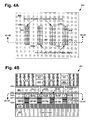
- Figure 4A shows a top view of structure 400 corresponding to a portion of a semiconductor die including a MOM capacitor having local interconnect metal plates 426a, 428a, 426b, and 428b, according to another embodiment of the present invention
- Figure 4B shows a cross-sectional view of structure 400 along perspective line 4B-4B in Figure 4A.
- Figure 4B also shows perspective line 4A-4A corresponding to the top view shown in Figure 4A .
- Figure 4A shows a top surface of local interlayer dielectric 444, cross-sections of vias 452 at substantially their respective points of contact with local interconnect metal plates 426a and 426b, and cross-sections of vias 454 at substantially their respective points of contact with local interconnect metal plates 428a and 428b.
- Local interlayer dielectric 444, vias 452, and vias 454 correspond respectively to local interlayer dielectric 244, vias 252, and vias 254, in Figures 2A and 2B .
- device layer 402, isolation region 406, local interlayer dielectrics 440, 442, 445, 446, and 448, first metallization segments 460, and dielectric bodies 470 of structure 400, and shown in Figure 4B correspond respectively to device layer 202, isolation region 206, local interlayer dielectrics 240, 242, 245, 246, and 248, first metallization segments 260, and dielectric bodies 270, in Figure 2B , and may share the characteristics previously attributed to those features, as described above.
- local interconnect metal plates 426a, 428a, 426b, and 428b, in Figures 4A and 4B share a common plane parallel to and below the plane of a first metallization layer from which first metallization segments 460 are formed.
- local interconnect metal plates 426a, 428a, 426b, and 428b are formed of local interconnect metal stacks including local interconnect metal bodies 422a, 424a, 422b, and 424b, respectively, formed over respective lower local interconnect metal bodies 412a, 414a, 412b, and 414b.
- local interconnect metal plates 426a, 428a, 426b, and 428a of the MOM capacitor embodied in Figures 4A and 4B may be formed from a local interconnect metal stack typically utilized in an MEOL process to provide source/drain connections for devices formed in device layer 402. Consequently, as was the case for the embodiments shown in Figures 1 , 2A , 2B , 3A, and 3B , the process for forming the embodiment shown by Figures 4A and 4B is compatible with standard CMOS fabrication process flows.
- the dielectric serving as the capacitor dielectric between local interconnect metal plates 526a and 528a and between local interconnect metal plates 526b and 528b is provided by a combination of local interlayer dielectrics 440, 442, and 444.
- the MOM capacitor dielectric may comprise a combination of SiO 2 and Si 3 N 4 and thus may have a dielectric constant greater than approximately 3.9 and less than approximately 7.0.
- the MOM capacitor dielectric implemented as part of the present invention may have a dielectric constant greater than or equal to approximately 3.9 and less than approximately 5.0.
- Figure 5A shows a top view of structure 500 corresponding to a portion of a semiconductor die including a MOM capacitor having local interconnect metal plates 526a, 528a, 526b, and 528b, according to another embodiment of the present invention
- Figure 5B shows a cross-sectional view of structure 500 along perspective line 5B-5B in Figure 5A.
- Figure 5B also shows perspective line 5A-5A corresponding to the top view shown in Figure 5A .
- Figure 5A shows a top surface of local interlayer dielectric 544, cross-sections of vias 552 at substantially their respective points of contact with local interconnect metal plates 526a and 526b, and cross-sections of vias 554 at substantially their respective points of contact with local interconnect metal plates 528a and 528b, as well as capacitor runner 532 interconnecting local interconnect metal plates 526a and 526b, and capacitor runner 534 interconnecting local interconnect metal plates 528a and 528b.
- local interconnect metal plates 526a and 526b are formed of local interconnect metal stacks including local interconnect metal bodies 522a and 522b, respectively, formed over respective lower local interconnect metal bodies 512a and 512b. It is noted that although local interconnect metal plates 528a and 528b are not visible in cross-section in Figure 5B , according to the present embodiment, local interconnect metal plates 528a and 528b are formed similarly to local interconnect metal plates 526a and 526b, and comprise a local interconnect metal body formed over a lower local interconnect metal body. In other words local interconnect metal plates 526a, 528a, 526b, and 528b correspond respectively to local interconnect metal plates 426a, 428a, 426b, and 428b, in Figure 4B .
- Local interlayer dielectric 544, vias 552, and vias 554 correspond respectively to local interlayer dielectric 444, vias 452, and vias 454, in Figures 4A and 4B .
- device layer 502, isolation region 506, local interlayer dielectrics 540, 542, 545, 546, and 548, first metallization segments 560, and dielectric bodies 570 of structure 500, in Figure 5B correspond respectively to device layer 402, isolation region 406, local interlayer dielectrics 440, 442, 445, 446, and 448, first metallization segments 460, and dielectric bodies 470, in Figure 4B , and may share the characteristics previously attributed to those features, as described above.
- FIG. 5A local interconnect metal plates 526a, 528a, 526b, 528b are arranged in interdigitated fashion.
- Figure 5A shows that local interconnect metal plates 526a and 526b are interconnected by capacitor runner 532 to form a MOM capacitor high terminal, while local interconnect metal plates 528a and 528b are interconnected by capacitor runner 534 to form a MOM capacitor low terminal.
- Capacitor runners 532 and 534 correspond respectively to capacitor runners 332 and 334 in Figures 3A and 3B , and like capacitor runners 332 and 334 are formed from a local interconnect metal.
- the present invention provides a MOM capacitor that utilizes one or more local interconnect metals, such as copper or a refractory metal such as tungsten, for example, to form capacitor plates, and utilizes a local interlayer dielectric, such as Si 3 N 4 and/or SiO 2 as the MOM capacitor dielectric.
- a local interlayer dielectric such as Si 3 N 4 and/or SiO 2 as the MOM capacitor dielectric.
- embodiments of the present MOM capacitor having local interconnect metal plates can be advantageously formed using established CMOS process flows during MEOL processing, without requiring substantial additional processing steps.
- embodiments of the present invention provide a MOM capacitor having an increased capacitance density compared to that achieved by conventional MOM capacitors fabricated between routing metallization layers during BEOL processing.
Landscapes
- Semiconductor Integrated Circuits (AREA)
- Internal Circuitry In Semiconductor Integrated Circuit Devices (AREA)
- Engineering & Computer Science (AREA)
- Power Engineering (AREA)
Abstract
Description
- The present invention is generally in the field of semiconductors. More particularly, the invention is in the field of fabrication of capacitors in semiconductor dies.
- Metal-oxide-metal (MOM) capacitors have been used extensively in the fabrication of integrated analog and mixed signal circuits on semiconductor dies. A MOM capacitor typically includes an oxide dielectric situated between adjacent metal plates, which form the electrodes of the MOM capacitor. Conventionally, MOM capacitors are fabricated on semiconductor dies during back-end-of-line (BEOL) processing.
- In the conventional approach, MOM capacitors are fabricated in the otherwise unused space available between routing metallization layers in a semiconductor die, during BEOL processing. However, the low dielectric constant (low-κ) of the dielectric materials typically present between routing metallization layers, such as materials having dielectric constants less than 3.0, for example, result in conventional MOM capacitors having relatively low capacitance densities. Although specialized dielectric materials can be use to form the MOM capacitor dielectric during BEOL, that alternative approach can require additional process steps and masks beyond those normally required for complementary metal-oxide-semiconductor (CMOS) fabrication process flows, which can undesirably increase manufacturing cost. Moreover, although it is desirable in principle to fabricate MOM capacitors having higher capacitance densities, situating such MOM capacitors between routing metallization layers formed over the device layer in which active devices are fabricated can adversely affect device performance, such as the speed of CMOS logic devices, for example.
- Thus, there is a need to overcome the drawbacks and deficiencies in the conventional art by providing a MOM capacitor capable of achieving a higher capacitance density while being compatible with standard CMOS fabrication materials and process flows.
- The present application is directed to a metal-oxide-metal (MOM) capacitor having local interconnect metal plates and related method, substantially as shown in and/or described in connection with at least one of the figures, and as set forth more completely in the claims.
- According to an aspect, a metal-oxide-metal (MOM) capacitor in a semiconductor die is provided, said MOM capacitor comprising:
- a first plurality of capacitor plates and a second plurality of capacitor plates sharing a plane parallel to and below a plane of a first metallization layer of said semiconductor die;
- a local interlayer dielectric between said first plurality of capacitor plates and said second plurality of capacitor plates;
- said first and second plurality of capacitor plates comprised of a local interconnect metal for connecting devices formed in a device layer situated below said first metallization layer.
- Advantageously, the MOM capacitor further comprises a first capacitor runner for interconnecting said first plurality of capacitor plates, and a second capacitor runner for interconnecting said second plurality of capacitor plates, said first and second capacitor runners comprising another local interconnect metal for providing connections among said devices formed in said device layer.
- Advantageously, said first plurality of capacitor plates further comprise a lower local interconnect metal, and said second plurality of capacitor plates further comprise said lower local interconnect metal.
- Advantageously, the MOM capacitor further comprises a first capacitor runner for interconnecting said first plurality of capacitor plates, and a second capacitor runner for interconnecting said second plurality of capacitor plates, said first and second capacitor runners comprising another local interconnect metal for providing connections among said devices formed in said device layer.
- Advantageously, said local interconnect metal comprises a refractory metal.
- Advantageously, said local interconnect metal comprises copper.
- Advantageously, said local interlayer dielectric comprises silicon oxide.
- Advantageously, said local interlayer dielectric comprises silicon nitride.
- Advantageously, said local interlayer dielectric has a dielectric constant greater than or equal to approximately 3.9 and less than approximately 5.0.
- Advantageously, said first and second plurality of capacitor plates are situated over an isolation region formed in said device layer.
- According to an aspect, a method for fabricating a metal-oxide-metal (MOM) capacitor in a semiconductor die comprises:
- forming a first plurality of capacitor plates and a second plurality of capacitor plates sharing a plane parallel to and below a plane of a first metallization layer of said semiconductor die, said first plurality of capacitor plates spaced from said second plurality of capacitor plates by a local interlayer dielectric;
- said first and second plurality of capacitor plates comprised of a local interconnect metal for connecting devices formed in a device layer situated below said first metallization layer.
- Advantageously, the method further comprises forming a first capacitor runner for interconnecting said first plurality of capacitor plates, and forming a second capacitor runner for interconnecting said second plurality of capacitor plates, said first and second capacitor runners comprising another local interconnect metal for providing connections among said devices formed in said device layer.
- Advantageously, said first plurality of capacitor plates further comprise a lower local interconnect metal, and said second plurality of capacitor plates further comprise said lower local interconnect metal.
- Advantageously, the method further comprises forming a first capacitor runner for interconnecting said first plurality of capacitor plates, and forming a second capacitor runner for interconnecting said second plurality of capacitor plates, said first and second capacitor runners comprising another local interconnect metal for providing connections among said devices formed in said device layer.
- Advantageously, said local interconnect metal comprises a refractory metal.
- Advantageously, said local interconnect metal comprises copper.
- Advantageously, said local interlayer dielectric comprises silicon oxide.
- Advantageously, said local interlayer dielectric comprises silicon nitride.
- Advantageously, said local interlayer dielectric has a dielectric constant greater than or equal to approximately 3.9 and less than approximately 5.0.
- Advantageously, forming said first and second plurality of capacitor plates comprises forming said first and second plurality of capacitor plates over an isolation region formed in said device layer.
-
-
Figure 1 shows a cross-sectional view of a portion of a semiconductor die including a metal-oxide-metal (MOM) capacitor having local interconnect metal plates, according to one embodiment of the present invention. -
Figure 2A shows a top view of a portion of a semiconductor die including a MOM capacitor having local interconnect metal plates alongperspective line 2A-2A inFigure 1 , according to one embodiment of the present invention. -
Figure 2B shows a cross-sectional view of the embodiment ofFigure 2A alongperspective line 2B-2B inFigure 2A . -
Figure 3A shows a top view of a portion of a semiconductor die including a MOM capacitor having local interconnect metal plates, according to another embodiment of the present invention. -
Figure 3B shows a cross-sectional view of the embodiment ofFigure 3A alongperspective line 3B-3B inFigure 3A . -
Figure 4A shows a top view of a portion of a semiconductor die including a MOM capacitor having local interconnect metal plates, according to another embodiment of the present invention. -
Figure 4B shows a cross-sectional view of the embodiment ofFigure 4A alongperspective line 4B-4B inFigure 4A . -
Figure 5A shows a top view of a portion of a semiconductor die including a MOM capacitor having local interconnect metal plates, according to another embodiment of the present invention. -
Figure 5B shows a cross-sectional view of the embodiment ofFigure 5A alongperspective line 5B-5B inFigure 5A . - The present application is directed to a metal-oxide-metal (MOM) capacitor having local interconnect metal plates and related method. Although the invention is described with respect to specific embodiments, the principles of the invention, as defined by the claims appended herein, can obviously be applied beyond the specifically described embodiments of the invention described herein. Moreover, in the description of the present invention, certain details have been left out in order to not obscure the inventive aspects of the invention. The details left out are within the knowledge of a person of ordinary skill in the art.
- The drawings in the present application and their accompanying detailed description are directed to merely example embodiments of the invention. To maintain brevity, other embodiments of the invention, which use the principles of the present invention, are not specifically described in the present application and are not specifically illustrated by the present drawings. It should be borne in mind that, unless noted otherwise, like or corresponding elements among the figures may be indicated by like or corresponding reference numerals. Moreover, the drawings and illustrations in the present application are generally not to scale, and are not intended to correspond to actual relative dimensions.
-
Figure 1 shows a cross-sectional view ofstructure 100, which includes a portion ofsemiconductor die 101 includingMOM capacitor 121 having localinterconnect metal plates structure 100 may be seen to correspond to a portion of a processed semiconductor die, which may include, among other features, a substrate, such as a group IV semiconductor substrate, a device layer, such asdevice layer 102, formed over the substrate, and isolation regions, such asisolation region 106. - As shown in
Figure 1 ,device layer 102, which can be an epitaxial semiconductor layer comprising silicon or germanium, for example, includes field-effect transistor (FET)region 103 andMOM capacitor region 104. FETregion 103 andMOM capacitor region 104 are regions ofdevice layer 102 that are designated for FET and MOM capacitor formation, respectively. As shown inFigure 1 , according to the present embodiment,FET region 103 ofdevice layer 102 includes source/drain regions dielectric layer 107, andgate 108 bordered byinsulating bodies 109, whileMOM capacitor region 104 includesisolation region 106, which can be, for example, a shallow trench isolation (STI) region formed indevice layer 102.Isolation region 106 can comprise silicon oxide (SiO2) or any other suitable dielectric material for formation ofisolation region 106, and insulatingbodies 109 can comprise any suitable dielectric, such as SiO2 or silicon nitride (Si3N4), for example. -
Device layer 102 includingFET region 103 andMOM capacitor region 104 is situated belowfirst metallization segments 160, which may be formed from an "M1" layer of semiconductor die 101, for example, providing routing metallization and fabricated during back-end-of-line (BEOL) processing of semiconductor die 101. It is noted thatfirst metallization segments 160 are separated bydielectric bodies 170, which may comprise low dielectric constant (low-K) dielectric bodies having a dielectric constant of approximately 2.55, for example. Situated betweendevice layer 102 andfirst metallization segments 160 are a series of local interlayer dielectrics, shown as local interlayerdielectric layers Figure 1 . Local interlayerdielectric layers dielectric layers dielectric layers -
Structure 100 further comprises lower localinterconnect metal body 110, localinterconnect metal body 120 formed over lower localinterconnect metal body 110, localinterconnect metal body 130 formed overgate 108, andMOM capacitor plates device layer 102, as well as to facilitate vertical connection of such devices to overlyingfirst metallization segments 160. A local interconnect metal may comprise copper (Cu), for example, or a refractory metal such as tungsten (W). Thus, lower localinterconnect metal body 110, localinterconnect metal body 120, localinterconnect metal body 130, and localinterconnect metal plates MOM capacitor 121 may comprise copper or a refractory metal such as tungsten, for example. - Lower local
interconnect metal body 110, localinterconnect metal body 120, localinterconnect metal body 130, and localinterconnect metal plates MOM capacitor 121 can be formed, for example, by appropriate patterning of local interlayerdielectric layers interconnect metal body 110 can be formed by patterning local interlayerdielectric layers interlayer dielectric layer 142 and a corresponding portion of localinterlayer dielectric layer 140 can be removed to expose source/drain region 1005b. Lower localinterconnect metal body 110 may then be formed in the opening produced thereby using any suitable deposition technique. Localinterconnect metal body 130 may be analogously formed through patterning of interlayerdielectric layers gate 108. Moreover, and as may be apparent fromFigure 1 , according to the present embodiment, localinterconnect metal body 120 and localinterconnect metal plates MOM capacitor 121 can be formed concurrently from the same local interconnect metal through appropriate patterning of localinterlayer dielectric layer 144, using a process that treatsinterlayer dielectric layer 142 as an etch stop surface. - Lower local
interconnect metal body 110 is situated over and makes electrical contact with source/drain region 105badjacent gate 108, and localinterconnect metal body 120 is formed over and makes electrical contact with lower localinterconnect metal body 110, while localinterconnect metal body 130 is formed so as to make electrical contact withgate 108. It is understood that source/drain regions gate 108 are part of a transistor fabricated inFET region 103, such that source/drain regions Figure 1 , lower localinterconnect metal body 110 and localinterconnect metal body 120 are configured to provide a source/drain connection for the transistor comprising source/drain regions gate 108, while localinterconnect metal body 130 is implemented to serve as a gate connection for that device. Moreover, it is noted that the local interconnect metals used respectively to form lower localinterconnect metal body 110 andlocal interconnect body 120 can be further implemented to connect source/drain region 105b to source drain regions of other devices formed in semiconductor die 101. In analogous manner, the local interconnect metal used to form localinterconnect metal body 130 can be further implemented to connectgate 108 to gates of other devices formed in semiconductor die 101. - Vertical contacts for connecting
gate 108, source/drain region 105b, andMOM capacitor 121 tofirst metallization segments 160 can be formed in local interlayerdielectric layers vias 152 in local interlayerdielectric layers vias 152 with tungsten or other metal or metal stack, as is known in the art. Moreover,first metallization segments 160 can comprise, for example, a metal such as aluminum or copper and can be formed by depositing and patterning a first metallization layer overdevice layer 102 and local interlayerdielectric layers - The advantages associated with various embodiments of the present invention will be further described in conjunction with
Figures 2A, 2B ,3A, 3B ,4A, 4B ,5A, and 5B of the present application. Referring first toFigures 2A and 2B, Figure 2A shows a top view ofstructure 200 corresponding to a portion of a semiconductor die includingMOM capacitor 221 having localinterconnect metal plates perspective line 2A-2A inFigure 1 , according to one embodiment of the present invention. In addition,Figure 2B shows a cross-sectional view ofstructure 200 alongperspective line 2B-2B inFigure 2A. Figure 2B also showsperspective line 2A-2A corresponding to the top view shown inFigure 2A as well as toperspective line 2A-2A inFigure 1 . - It is noted that the portion of semiconductor die 101, in
Figure 1 , represented bystructure 200, inFigures 2A and 2B , corresponds toMOM capacitor region 103, inFigure 1 , and depicts more ofMOM capacitor region 103 than is shown bystructure 100. Thus, it may be understood that localinterconnect metal plates MOM capacitor 221, inFigures 2A and 2B , correspond respectively to localinterconnect metal plates MOM capacitor 121, inFigure 1 , while localinterconnect metal plates 222b and 224b, inFigures 2A and 2B , are situated in a portion ofMOM capacitor region 103, inFigure 1 , that is out of view inFigure 1 . - In addition to local
interconnect metal plates MOM capacitor 221,Figure 2A shows a top surface oflocal interlayer dielectric 244, cross-sections ofvias 252 at substantially their respective points of contact with localinterconnect metal plates vias 254 at substantially their respective points of contact with localinterconnect metal plates 224a and 224b.Local interlayer dielectric 244 and vias 252 correspond respectively to localinterlayer dielectric layer 144 and via 152 in contact with localinterconnect metal plate 122, inFigure 1 . It is noted thatvias 254 in contact with localinterconnect metal plates 224a and 224b, shown inFigure 2A , correspond to features that may be present instructure 100 ofFigure 1 , but are out of view from the perspective ofFigure 1 , and are also out of view inFigure 2B . In addition to the features shown inFigure 2A, Figure 2B showsdevice layer 202,isolation region 206,local interlayer dielectrics first metallization segments 260, anddielectric bodies 270 ofstructure 200, corresponding respectively todevice layer 102,isolation region 106, local interlayerdielectric layers first metallization segments 160, anddielectric bodies 170 ofstructure 100, inFigure 1 . - As shown in
Figure 2A ,MOM capacitor 221 comprises a first plurality of capacitor plates, e.g., localinterconnect metal plates MOM capacitor 221 in the present embodiment. In addition,MOM capacitor 221 comprises a second plurality of capacitors plates, e.g., localinterconnect metal plates 224a and 224b identified as low terminal plates ofMOM capacitor 221 in the present embodiment. As may be seen fromFigures 2A and 2B , localinterconnect metal plates first metallization segments 260 are formed. That is to say, from the perspective shown byFigure 2B , the plane shared byfirst metallization segments 260 and the parallel plane shared by localinterconnect metal plates first metallization segments 260 lie substantially perpendicular to the page occupied byFigures 2A and 2B . Moreover, it is noted that according to the embodiment shown byFigures 2A and 2B , localinterconnect metal plates isolation region 206, which is formed indevice layer 202, as also shown inFigure 1 . - As further shown in
Figures 2A and 2B ,local interlayer dielectric 244 is disposed between the first plurality of capacitor plates represented by localinterconnect metal plates interconnect metal plates 224a and 224b. Consequently,local interlayer dielectric 244 is utilized as a capacitor dielectric forMOM capacitor 221. In one embodiment, for example, as discussed above,local interlayer dielectric 244 may comprise SiO2, in which case a dielectric constant associated with the capacitor dielectric utilized inMOM capacitor 221 would be substantially equal to approximately 3.9. - As noted above, local
interconnect metal plates device layer 202, as well as to facilitate vertical connection of those devices to overlyingfirst metallization segments 260, and may comprise copper or a refractory metal such as tungsten. In one embodiment, for example, the local interconnect metals used to form lower localinterconnect metal body 110, localinterconnect metal body 120, and localinterconnect metal body 130, inFigure 1 , may serve specific functions at a particular technology node. For instance, at the 20.0 nanometer (20 nm) node, a local interconnect metal or metals used to form lower localinterconnect metal body 110 and localinterconnect metal body 120 may typically be utilized in a middle-of-the-line (MEOL) process to provide source/drain connections for devices formed indevice layer 102. According to embodiments of the present invention, however, at least one local interconnect metal, e.g., the local interconnect metal used to form localinterconnect metal body 120, can additionally be advantageously used to fabricate localinterconnect metal plates MOM capacitor 221. -
MOM capacitor 221 is situated between first metallization segments 260 (e.g., segments formed from a first routing metallization layer ofstructure 200, fabricated during BEOL processing) anddevice layer 202. Thus, both the high and low terminal electrodes ofMOM capacitor 221 are formed of a local interconnect metal used belowfirst metallization segments 260 during MEOL processing. In addition, use of a local interlayer dielectric, such aslocal interlayer dielectric 244, as the capacitor dielectric forMOM capacitor 221, renders a process for formingMOM capacitor 221 compatible with standard MEOL fabrication processing steps for advanced process technologies, such as 20 nm and smaller complementary metal-oxide-semiconductor (CMOS) process technologies, for example. - As explained above, according to the present embodiment,
MOM capacitor 221 is situated overisolation region 206. In addition, the embodiment shown inFigure 2B achieves additional isolation and noise protection by providinglocal interlayer dielectrics MOM capacitor 221 anddevice layer 202. Furthermore, by utilizing a local interlayer dielectric having a dielectric constant of approximately 3.9, or greater iflocal interlayer dielectric 244 comprises Si3N4, for example,MOM capacitor 221 can achieve a capacitance density greater than that achievable by conventional MOM capacitors formed between routing metallization layers in a semiconductor die during BEOL processing and utilizing the low-K dielectric materials typically formed in those regions as the MOM capacitor dielectric. - Moving now to
Figures 3A and 3B, Figure 3A shows a top view ofstructure 300 corresponding to a portion of a semiconductor die including a MOM capacitor having localinterconnect metal plates Figure 3B shows a cross-sectional view ofstructure 300 alongperspective line 3B-3B inFigure 3A. Figure 3B also showsperspective line 3A-3A corresponding to the top view shown inFigure 3A . - In addition to local
interconnect metal plates Figure 3A shows a top surface oflocal interlayer dielectric 344, cross-sections ofvias 352 at substantially their respective points of contact with localinterconnect metal plates vias 354 at substantially their respective points of contact with localinterconnect metal plates capacitor runner 332 interconnecting localinterconnect metal plates capacitor runner 334 interconnecting localinterconnect metal plates interconnect metal plates local interlayer dielectric 344, vias 352, and vias 354 correspond respectively to localinterconnect metal plates local interlayer dielectric 244, vias 252, and vias 254, inFigures 2A and 2B . Moreover, it is noted thatdevice layer 302,isolation region 306,local interlayer dielectrics first metallization segments 360, anddielectric bodies 370 ofstructure 300, shown inFigure 3B , correspond respectively todevice layer 202,isolation region 206,local interlayer dielectrics first metallization segments 260, anddielectric bodies 270, inFigure 2B , and may share the characteristics previously attributed to those features, as described in detail above. - As shown in
Figure 3A , localinterconnect metal plates Figure 3A shows that localinterconnect metal plates capacitor runner 332 to form a MOM capacitor high terminal, while localinterconnect metal plates capacitor runner 334 to form a MOM capacitor low terminal. As further shown byFigure 3A ,capacitor runners interconnect metal plates capacitor runners interconnect metal plates - According to the embodiment shown in
Figures 3A and 3B ,capacitor runners Figure 1 withFigures 3A and 3B reveals that, according to the present embodiment,capacitor runners interconnect metal body 130, inFigure 1 . As previously discussed, the local interconnect metal used to form localinterconnect metal body 130 may serve a specific function at a particular technology node. Using the 20 nm node again as an example, a local interconnect metal used to form localinterconnect metal body 130 may typically be utilized in an MEOL process as gate connections for devices formed indevice layer 102. According to embodiments of the present invention, however, a local interconnect metal, e.g., the local interconnect metal used to form localinterconnect metal body 120, can be advantageously used to fabricate localinterconnect metal plates interconnect metal body 130, can be further advantageously used to fabricatecapacitor runners interconnect metal plates Figures 1 ,2A, and 2B , the process for forming the embodiments ofFigures 3A and 3B is compatible with standard fabrication processes for advanced process technologies. - Referring to
Figures 4A and 4B, Figure 4A shows a top view ofstructure 400 corresponding to a portion of a semiconductor die including a MOM capacitor having localinterconnect metal plates Figure 4B shows a cross-sectional view ofstructure 400 alongperspective line 4B-4B inFigure 4A. Figure 4B also showsperspective line 4A-4A corresponding to the top view shown inFigure 4A . - In addition to local
interconnect metal plates Figure 4A shows a top surface oflocal interlayer dielectric 444, cross-sections ofvias 452 at substantially their respective points of contact with localinterconnect metal plates vias 454 at substantially their respective points of contact with localinterconnect metal plates Local interlayer dielectric 444, vias 452, and vias 454 correspond respectively tolocal interlayer dielectric 244, vias 252, and vias 254, inFigures 2A and 2B . Moreover, it is noted thatdevice layer 402,isolation region 406,local interlayer dielectrics first metallization segments 460, anddielectric bodies 470 ofstructure 400, and shown inFigure 4B , correspond respectively todevice layer 202,isolation region 206,local interlayer dielectrics first metallization segments 260, anddielectric bodies 270, inFigure 2B , and may share the characteristics previously attributed to those features, as described above. - Like local
interconnect metal plates Figures 2A and 2B , localinterconnect metal plates Figures 4A and 4B share a common plane parallel to and below the plane of a first metallization layer from whichfirst metallization segments 460 are formed. In addition, however, and as shown inFigure 4B , localinterconnect metal plates interconnect metal bodies 422a, 424a, 422b, and 424b, respectively, formed over respective lower localinterconnect metal bodies Figure 1 withFigures 4A and 4B reveals that, according to the present embodiment, lower localinterconnect metal bodies Figure 4B , are formed from the same lower local interconnect metal used to form lower localinterconnect metal body 110, inFigure 1 , while localinterconnect metal bodies 422a, 424a, 422b, and 424b, inFigure 4B , are formed from the same local interconnect metal used to form localinterconnect metal body 120, inFigure 1 . Thus, localinterconnect metal plates Figures 4A and 4B may be formed from a local interconnect metal stack typically utilized in an MEOL process to provide source/drain connections for devices formed indevice layer 402. Consequently, as was the case for the embodiments shown inFigures 1 ,2A ,2B ,3A, and 3B , the process for forming the embodiment shown byFigures 4A and 4B is compatible with standard CMOS fabrication process flows. - According to the embodiment of
Figures 4A and 4B , and as further shown byFigure 4B , the dielectric serving as the capacitor dielectric between localinterconnect metal plates interconnect metal plates 526b and 528b is provided by a combination oflocal interlayer dielectrics local interlayer dielectrics - Continuing to
Figures 5A and 5B, Figure 5A shows a top view ofstructure 500 corresponding to a portion of a semiconductor die including a MOM capacitor having localinterconnect metal plates Figure 5B shows a cross-sectional view ofstructure 500 alongperspective line 5B-5B inFigure 5A. Figure 5B also showsperspective line 5A-5A corresponding to the top view shown inFigure 5A . - In addition to local
interconnect metal plates Figure 5A shows a top surface oflocal interlayer dielectric 544, cross-sections ofvias 552 at substantially their respective points of contact with localinterconnect metal plates vias 554 at substantially their respective points of contact with localinterconnect metal plates 528a and 528b, as well ascapacitor runner 532 interconnecting localinterconnect metal plates capacitor runner 534 interconnecting localinterconnect metal plates 528a and 528b. - As shown in
Figure 5B , localinterconnect metal plates interconnect metal bodies 522a and 522b, respectively, formed over respective lower localinterconnect metal bodies 512a and 512b. It is noted that although localinterconnect metal plates 528a and 528b are not visible in cross-section inFigure 5B , according to the present embodiment, localinterconnect metal plates 528a and 528b are formed similarly to localinterconnect metal plates interconnect metal plates interconnect metal plates Figure 4B . -
Local interlayer dielectric 544, vias 552, and vias 554 correspond respectively tolocal interlayer dielectric 444, vias 452, and vias 454, inFigures 4A and 4B . Moreover, it is noted thatdevice layer 502,isolation region 506,local interlayer dielectrics first metallization segments 560, anddielectric bodies 570 ofstructure 500, inFigure 5B , correspond respectively todevice layer 402,isolation region 406,local interlayer dielectrics first metallization segments 460, anddielectric bodies 470, inFigure 4B , and may share the characteristics previously attributed to those features, as described above. - As shown in
Figure 5A , localinterconnect metal plates Figure 5A shows that localinterconnect metal plates capacitor runner 532 to form a MOM capacitor high terminal, while localinterconnect metal plates 528a and 528b are interconnected bycapacitor runner 534 to form a MOM capacitor low terminal.Capacitor runners capacitor runners Figures 3A and 3B , and likecapacitor runners - Thus, as discussed above, the present invention provides a MOM capacitor that utilizes one or more local interconnect metals, such as copper or a refractory metal such as tungsten, for example, to form capacitor plates, and utilizes a local interlayer dielectric, such as Si3N4 and/or SiO2 as the MOM capacitor dielectric. As a result, embodiments of the present MOM capacitor having local interconnect metal plates can be advantageously formed using established CMOS process flows during MEOL processing, without requiring substantial additional processing steps. Moreover; embodiments of the present invention provide a MOM capacitor having an increased capacitance density compared to that achieved by conventional MOM capacitors fabricated between routing metallization layers during BEOL processing.
- From the above description of the invention it is manifest that various techniques can be used for implementing the concepts of the present invention without departing from its scope. Moreover, while the invention has been described with specific reference to certain embodiments, a person of ordinary skill in the art would appreciate that changes can be made in form and detail without departing from the spirit and the scope of the invention. Thus, the described embodiments are to be considered in all respects as illustrative and not restrictive. It should also be understood that the invention is not limited to the particular embodiments described herein but is capable of many rearrangements, modifications, and substitutions without departing from the scope of the invention.
Claims (15)
- A metal-oxide-metal (MOM) capacitor in a semiconductor die, said MOM capacitor comprising:a first plurality of capacitor plates and a second plurality of capacitor plates sharing a plane parallel to and below a plane of a first metallization layer of said semiconductor die;a local interlayer dielectric between said first plurality of capacitor plates and said second plurality of capacitor plates;said first and second plurality of capacitor plates comprised of a local interconnect metal for connecting devices formed in a device layer situated below said first metallization layer.
- The MOM capacitor of claim 1, further comprising a first capacitor runner for interconnecting said first plurality of capacitor plates, and a second capacitor runner for interconnecting said second plurality of capacitor plates, said first and second capacitor runners comprising another local interconnect metal for providing connections among said devices formed in said device layer.
- The MOM capacitor of claim 1, wherein said first plurality of capacitor plates further comprise a lower local interconnect metal, and said second plurality of capacitor plates further comprise said lower local interconnect metal.
- The MOM capacitor of claim 3, further comprising a first capacitor runner for interconnecting said first plurality of capacitor plates, and a second capacitor runner for interconnecting said second plurality of capacitor plates, said first and second capacitor runners comprising another local interconnect metal for providing connections among said devices formed in said device layer.
- The MOM capacitor of claim 1, wherein said local interconnect metal comprises a refractory metal.
- The MOM capacitor of claim 1, wherein said local interconnect metal comprises copper.
- The MOM capacitor of claim 1, wherein said local interlayer dielectric comprises silicon oxide.
- The MOM capacitor of claim 1, wherein said local interlayer dielectric comprises silicon nitride.
- The MOM capacitor of claim 1, wherein said local interlayer dielectric has a dielectric constant greater than or equal to approximately 3.9 and less than approximately 5.0.
- The MOM capacitor of claim 1, wherein said first and second plurality of capacitor plates are situated over an isolation region formed in said device layer.
- A method for fabricating a metal-oxide-metal (MOM) capacitor in a semiconductor die, said method comprising:forming a first plurality of capacitor plates and a second plurality of capacitor plates sharing a plane parallel to and below a plane of a first metallization layer of said semiconductor die, said first plurality of capacitor plates spaced from said second plurality of capacitor plates by a local interlayer dielectric;said first and second plurality of capacitor plates comprised of a local interconnect metal for connecting devices formed in a device layer situated below said first metallization layer.
- The method of claim 11, further comprising forming a first capacitor runner for interconnecting said first plurality of capacitor plates, and forming a second capacitor runner for interconnecting said second plurality of capacitor plates, said first and second capacitor runners comprising another local interconnect metal for providing connections among said devices formed in said device layer.
- The method of claim 11, wherein said first plurality of capacitor plates further comprise a lower local interconnect metal, and said second plurality of capacitor plates further comprise said lower local interconnect metal.
- The method of claim 13, further comprising forming a first capacitor runner for interconnecting said first plurality of capacitor plates, and forming a second capacitor runner for interconnecting said second plurality of capacitor plates, said first and second capacitor runners comprising another local interconnect metal for providing connections among said devices formed in said device layer.
- The method of claim 11, wherein said local interconnect metal comprises a refractory metal.
Applications Claiming Priority (1)
| Application Number | Priority Date | Filing Date | Title |
|---|---|---|---|
| US13/270,452 US8890288B2 (en) | 2011-10-11 | 2011-10-11 | MOM capacitor having local interconnect metal plates and related method |
Publications (2)
| Publication Number | Publication Date |
|---|---|
| EP2581935A2 true EP2581935A2 (en) | 2013-04-17 |
| EP2581935A3 EP2581935A3 (en) | 2013-10-02 |
Family
ID=47071049
Family Applications (1)
| Application Number | Title | Priority Date | Filing Date |
|---|---|---|---|
| EP12006690.7A Ceased EP2581935A3 (en) | 2011-10-11 | 2012-09-25 | MOM capacitor having electrodes made from local interconnects and manufacturing method thereof |
Country Status (4)
| Country | Link |
|---|---|
| US (1) | US8890288B2 (en) |
| EP (1) | EP2581935A3 (en) |
| CN (2) | CN203192792U (en) |
| TW (1) | TWI487122B (en) |
Cited By (1)
| Publication number | Priority date | Publication date | Assignee | Title |
|---|---|---|---|---|
| WO2016039968A1 (en) * | 2014-09-12 | 2016-03-17 | Qualcomm Incorporated | MIDDLE-OF-LINE (MOL) MANUFACTURED INTEGRATED CIRCUITS (ICs) EMPLOYING LOCAL INTERCONNECTS OF METAL LINES USING AN ELONGATED VIA, AND RELATED METHODS |
Families Citing this family (5)
| Publication number | Priority date | Publication date | Assignee | Title |
|---|---|---|---|---|
| US8890288B2 (en) * | 2011-10-11 | 2014-11-18 | Broadcom Corporation | MOM capacitor having local interconnect metal plates and related method |
| US9401357B2 (en) | 2014-02-28 | 2016-07-26 | Qualcomm Incorporated | Directional FinFET capacitor structures |
| US10031989B2 (en) | 2014-11-18 | 2018-07-24 | Globalfoundries Inc. | Integrated circuit performance modeling using a connectivity-based condensed resistance model for a conductive structure in an integrated circuit |
| US10692808B2 (en) | 2017-09-18 | 2020-06-23 | Qualcomm Incorporated | High performance cell design in a technology with high density metal routing |
| US12490504B2 (en) | 2022-02-07 | 2025-12-02 | Qualcomm Incorporated | High density linear capacitor in semiconductor technologies |
Citations (1)
| Publication number | Priority date | Publication date | Assignee | Title |
|---|---|---|---|---|
| US6383858B1 (en) * | 2000-02-16 | 2002-05-07 | Agere Systems Guardian Corp. | Interdigitated capacitor structure for use in an integrated circuit |
Family Cites Families (10)
| Publication number | Priority date | Publication date | Assignee | Title |
|---|---|---|---|---|
| JP2001223269A (en) * | 2000-02-10 | 2001-08-17 | Nec Corp | Semiconductor device and method of manufacturing the same |
| US6819542B2 (en) | 2003-03-04 | 2004-11-16 | Taiwan Semiconductor Manufacturing Co., Ltd. | Interdigitated capacitor structure for an integrated circuit |
| KR100688499B1 (en) * | 2004-08-26 | 2007-03-02 | 삼성전자주식회사 | MIM capacitor comprising a dielectric film having a crystallization preventing film and a method of manufacturing the same |
| KR100703974B1 (en) * | 2005-08-11 | 2007-04-06 | 삼성전자주식회사 | Semiconductor integrated circuit device including MIM capacitor and its manufacturing method |
| US7514740B2 (en) * | 2006-07-10 | 2009-04-07 | Taiwan Semiconductor Manufacturing Company, Ltd. | Logic compatible storage device |
| US8243510B2 (en) * | 2006-08-30 | 2012-08-14 | Broadcom Corporation | Non-volatile memory cell with metal capacitor |
| US8022458B2 (en) * | 2007-10-08 | 2011-09-20 | Taiwan Semiconductor Manufacturing Company, Ltd. | Capacitors integrated with metal gate formation |
| US8569807B2 (en) * | 2009-09-01 | 2013-10-29 | Taiwan Semiconductor Manufacturing Company, Ltd. | Backside illuminated image sensor having capacitor on pixel region |
| US20130140573A1 (en) * | 2010-06-07 | 2013-06-06 | Yoshinobu Nakamura | Manufacturing method for crystalline semiconductor film, semiconductor device, and display device |
| US8890288B2 (en) * | 2011-10-11 | 2014-11-18 | Broadcom Corporation | MOM capacitor having local interconnect metal plates and related method |
-
2011
- 2011-10-11 US US13/270,452 patent/US8890288B2/en active Active
-
2012
- 2012-09-17 TW TW101133995A patent/TWI487122B/en not_active IP Right Cessation
- 2012-09-24 CN CN2012204912671U patent/CN203192792U/en not_active Expired - Fee Related
- 2012-09-24 CN CN2012103598501A patent/CN103117268A/en active Pending
- 2012-09-25 EP EP12006690.7A patent/EP2581935A3/en not_active Ceased
Patent Citations (1)
| Publication number | Priority date | Publication date | Assignee | Title |
|---|---|---|---|---|
| US6383858B1 (en) * | 2000-02-16 | 2002-05-07 | Agere Systems Guardian Corp. | Interdigitated capacitor structure for use in an integrated circuit |
Cited By (6)
| Publication number | Priority date | Publication date | Assignee | Title |
|---|---|---|---|---|
| WO2016039968A1 (en) * | 2014-09-12 | 2016-03-17 | Qualcomm Incorporated | MIDDLE-OF-LINE (MOL) MANUFACTURED INTEGRATED CIRCUITS (ICs) EMPLOYING LOCAL INTERCONNECTS OF METAL LINES USING AN ELONGATED VIA, AND RELATED METHODS |
| US9620454B2 (en) | 2014-09-12 | 2017-04-11 | Qualcomm Incorporated | Middle-of-line (MOL) manufactured integrated circuits (ICs) employing local interconnects of metal lines using an elongated via, and related methods |
| CN106716631A (en) * | 2014-09-12 | 2017-05-24 | 高通股份有限公司 | Integrated circuit (IC) fabricated using metal line local interconnect using extended vias and related methods |
| CN106716631B (en) * | 2014-09-12 | 2020-06-26 | 高通股份有限公司 | Integrated Circuits (ICs) fabricated using mid-line-of-line (MOL) local interconnects of metal lines using extended vias and related methods |
| CN111584459A (en) * | 2014-09-12 | 2020-08-25 | 高通股份有限公司 | Integrated circuit IC and related method fabricated using mid-process MOL using metal line local interconnection using extended vias |
| CN111584459B (en) * | 2014-09-12 | 2024-06-07 | 高通股份有限公司 | Integrated circuit IC fabricated using a mid-stage process MOL for metal line local interconnect using extended vias and related methods |
Also Published As
| Publication number | Publication date |
|---|---|
| US8890288B2 (en) | 2014-11-18 |
| TWI487122B (en) | 2015-06-01 |
| CN103117268A (en) | 2013-05-22 |
| TW201324791A (en) | 2013-06-16 |
| EP2581935A3 (en) | 2013-10-02 |
| US20130087886A1 (en) | 2013-04-11 |
| CN203192792U (en) | 2013-09-11 |
Similar Documents
| Publication | Publication Date | Title |
|---|---|---|
| US10373905B2 (en) | Integrating metal-insulator-metal capacitors with air gap process flow | |
| US7768130B2 (en) | BEOL interconnect structures with simultaneous high-k and low-k dielectric regions | |
| US9041153B2 (en) | MIM capacitor having a local interconnect metal electrode and related structure | |
| US6940114B2 (en) | Integrated circuit devices including a MIM capacitor | |
| US8872248B2 (en) | Capacitors comprising slot contact plugs | |
| US8890288B2 (en) | MOM capacitor having local interconnect metal plates and related method | |
| US11854959B2 (en) | Metal-insulator-metal device with improved performance | |
| CN101211849B (en) | Semiconductor device capacitance preparation method | |
| US20220140109A1 (en) | Gate structure and methods thereof | |
| US20240072050A1 (en) | Field-effect transistors with isolation pillars | |
| US20240274653A1 (en) | Metal-insulator-metal structure | |
| US12362278B2 (en) | Transistors with dual power and signal lines | |
| US20250323141A1 (en) | Semiconductor structure and method for manufacturing the same | |
| US20240120369A1 (en) | High density trench capacitor | |
| HK1183560A (en) | Mom capacitor having local interconnect metal plates and related method | |
| US20240145472A1 (en) | Semiconductor structure with dielectric pillars | |
| US8846462B2 (en) | Transistor level routing | |
| CN222619763U (en) | Integrated circuit | |
| US20240014264A1 (en) | Single diffusion break |
Legal Events
| Date | Code | Title | Description |
|---|---|---|---|
| PUAI | Public reference made under article 153(3) epc to a published international application that has entered the european phase |
Free format text: ORIGINAL CODE: 0009012 |
|
| AK | Designated contracting states |
Kind code of ref document: A2 Designated state(s): AL AT BE BG CH CY CZ DE DK EE ES FI FR GB GR HR HU IE IS IT LI LT LU LV MC MK MT NL NO PL PT RO RS SE SI SK SM TR |
|
| AX | Request for extension of the european patent |
Extension state: BA ME |
|
| PUAL | Search report despatched |
Free format text: ORIGINAL CODE: 0009013 |
|
| AK | Designated contracting states |
Kind code of ref document: A3 Designated state(s): AL AT BE BG CH CY CZ DE DK EE ES FI FR GB GR HR HU IE IS IT LI LT LU LV MC MK MT NL NO PL PT RO RS SE SI SK SM TR |
|
| AX | Request for extension of the european patent |
Extension state: BA ME |
|
| RIC1 | Information provided on ipc code assigned before grant |
Ipc: H01L 27/06 20060101ALI20130823BHEP Ipc: H01L 49/02 20060101ALI20130823BHEP Ipc: H01L 23/522 20060101ALI20130823BHEP Ipc: H01L 21/768 20060101AFI20130823BHEP |
|
| 17P | Request for examination filed |
Effective date: 20140402 |
|
| RBV | Designated contracting states (corrected) |
Designated state(s): AL AT BE BG CH CY CZ DE DK EE ES FI FR GB GR HR HU IE IS IT LI LT LU LV MC MK MT NL NO PL PT RO RS SE SI SK SM TR |
|
| RAP1 | Party data changed (applicant data changed or rights of an application transferred) |
Owner name: AVAGO TECHNOLOGIES GENERAL IP (SINGAPORE) PTE. LTD |
|
| STAA | Information on the status of an ep patent application or granted ep patent |
Free format text: STATUS: EXAMINATION IS IN PROGRESS |
|
| 17Q | First examination report despatched |
Effective date: 20180927 |
|
| RAP1 | Party data changed (applicant data changed or rights of an application transferred) |
Owner name: AVAGO TECHNOLOGIES INTERNATIONAL SALES PTE. LIMITE |
|
| STAA | Information on the status of an ep patent application or granted ep patent |
Free format text: STATUS: THE APPLICATION HAS BEEN REFUSED |
|
| 18R | Application refused |
Effective date: 20210713 |