EP2579575A1 - Method for acquiring data with an image sensor - Google Patents
Method for acquiring data with an image sensor Download PDFInfo
- Publication number
- EP2579575A1 EP2579575A1 EP11184107.8A EP11184107A EP2579575A1 EP 2579575 A1 EP2579575 A1 EP 2579575A1 EP 11184107 A EP11184107 A EP 11184107A EP 2579575 A1 EP2579575 A1 EP 2579575A1
- Authority
- EP
- European Patent Office
- Prior art keywords
- pixel
- read
- reset
- value
- sensor
- Prior art date
- Legal status (The legal status is an assumption and is not a legal conclusion. Google has not performed a legal analysis and makes no representation as to the accuracy of the status listed.)
- Withdrawn
Links
Images

Classifications
-
- H—ELECTRICITY
- H04—ELECTRIC COMMUNICATION TECHNIQUE
- H04N—PICTORIAL COMMUNICATION, e.g. TELEVISION
- H04N25/00—Circuitry of solid-state image sensors [SSIS]; Control thereof
-
- H—ELECTRICITY
- H04—ELECTRIC COMMUNICATION TECHNIQUE
- H04N—PICTORIAL COMMUNICATION, e.g. TELEVISION
- H04N23/00—Cameras or camera modules comprising electronic image sensors; Control thereof
- H04N23/30—Cameras or camera modules comprising electronic image sensors; Control thereof for generating image signals from X-rays
-
- H—ELECTRICITY
- H04—ELECTRIC COMMUNICATION TECHNIQUE
- H04N—PICTORIAL COMMUNICATION, e.g. TELEVISION
- H04N25/00—Circuitry of solid-state image sensors [SSIS]; Control thereof
- H04N25/60—Noise processing, e.g. detecting, correcting, reducing or removing noise
- H04N25/616—Noise processing, e.g. detecting, correcting, reducing or removing noise involving a correlated sampling function, e.g. correlated double sampling [CDS] or triple sampling
-
- H—ELECTRICITY
- H04—ELECTRIC COMMUNICATION TECHNIQUE
- H04N—PICTORIAL COMMUNICATION, e.g. TELEVISION
- H04N25/00—Circuitry of solid-state image sensors [SSIS]; Control thereof
- H04N25/70—SSIS architectures; Circuits associated therewith
- H04N25/76—Addressed sensors, e.g. MOS or CMOS sensors
-
- H—ELECTRICITY
- H10—SEMICONDUCTOR DEVICES; ELECTRIC SOLID-STATE DEVICES NOT OTHERWISE PROVIDED FOR
- H10F—INORGANIC SEMICONDUCTOR DEVICES SENSITIVE TO INFRARED RADIATION, LIGHT, ELECTROMAGNETIC RADIATION OF SHORTER WAVELENGTH OR CORPUSCULAR RADIATION
- H10F39/00—Integrated devices, or assemblies of multiple devices, comprising at least one element covered by group H10F30/00, e.g. radiation detectors comprising photodiode arrays
- H10F39/10—Integrated devices
- H10F39/12—Image sensors
Definitions
- the invention relates to a method for acquiring data with an image sensor, the sensor showing a multitude of pixels, the sensor using a reset to bring the pixels to a predetermined state, the method comprising the steps of resetting the voltage of a pixel, reading the voltage of the pixel a first time, resulting in a first read-out value for the pixel, reading the voltage of each pixel a second time, resulting in a second read-out value for the pixel, and determining the difference between the first and the second read-out value of the pixel.
- CDS Correlative Double Sampling
- FPN Fixed Pattern Noise
- RN Reset Noise
- CMOS sensor a large number of sensitive elements, further referred to as pixels, in the form of photo diodes are arranged in an array. Each of these pixels can be selectively connected to an Analogue-to-Digital Convertor (ADC), and the voltage over the pixel is digitized. The voltage over the pixels is a result of impinging radiation, such as light.
- ADC Analogue-to-Digital Convertor
- CMOS detector is often equipped with a multitude of ADC's, each ADC assigned to a group of pixels.
- the voltage over the pixel after a reset varies from reset to reset.
- the signal without reset noise can be determined by subtracting the two values from each other.
- a disadvantage for said CDS method is that for each image all pixels of the sensor need to be read-out twice. This limits the maximum frame-rate with which the sensor can be read-out, and introducing CDS effectively halves the frame rate.
- single particle detection When using an image sensor for direct particle detection, such as direct electron detection, single particle detection is preferred. Also when using X-rays single event detection is preferred to determine the energy of the X-ray photon, and to distinguish between, for example, two low energy photons from one high energy photon. The occurrence of a single particle or X-ray photon impinging on the detector is then determined by the signal on one or a group of neighboring pixels. The read-out speed of the sensor must be sufficiently high to have a negligible chance that two particles or photons are detected by one pixel between read-outs. The reason is that the signal that is generated by an impinging particle can vary and therefore the difference between e.g. one and two, or three and four particles cannot be determined reliably.
- CMOS Pixel Sensor Response to Low Energy Electrons in Transmission Electron Microscopy For a description of the variation of the signal resulting from one impinging electron, see for example "CMOS Pixel Sensor Response to Low Energy Electrons in Transmission Electron Microscopy", M. Battaglia et al., Nuclear Instruments and Methods in Physics Research Section A: Accelerators, Spectrometers, Detectors and Associated Equipment (2009), Vol. 605, Issue: 3, pages 350-35 (further referred to as Battaglia), specifically figure 1 .
- the invention is based on the insight that the capacity of the well (the amount of charge or signal or voltage that can be stored in a pixel) before it overflows, the so-called full-well capacity, is many times larger than the charge resulting from one impinging particle. Typically the full-well capacity corresponds with at least 10 incident particles.
- the prior art CDS method uses 2xM read-out cycles, while when using the method according to the invention only M+1 read-out cycles are needed. The result is thus a much improved read-out speed.
- the invention is particularly valuable as the method can be performed on a standard, unmodified sensor.
- the invention is used to detect particles, such a neutrons, positrons, electrons, and/or X-rays.
- Such particles are typically detected with a flux that is low compared to the flux of photons when detecting light. The chance that a multitude of events occurs at one pixel is often negligible. Also earlier mentioned particle counting is often preferred.
- the method according to the invention offering a higher frame-rate than the prior art method, is then better suited than the prior art method.
- the method can also be used when detecting light, but it is unlikely that a fast read-out is required while no overflow of a well occur, or that photon counting is used. However, should this be preferred, for example for photon counting, the method according to the invention can be advantageous.
- the difference between two subsequently acquired data can be compared to the minimum that an impinging particle would cause.
- the signal can then be expressed as the number of impinging particles per pixel.
- particle counting results in a better signal-to-noise ratio than analogue processing.
- the detection of a particle is deduced from the (change of) signal of a group of adjacent pixels.
- one particle such as an electron
- a signal in several adjacent pixels see for example Battaglia.
- the occurrence of an event and the position of the event may be derived from the signal of several adjacent pixels, for example a group of 4 x 4 pixels.
- the CMOS sensor is reset, either after a predetermined number of read-outs (images) since the last reset, or after detecting that at least one pixel in the series of read-out forming the last frame has a charge above a predetermined value (typically close to the full-well value, for example 0.8 times the full-well value).
- the pixels are reset one at a time, when it is determined that they approach the full-well value. This, however, will probably involve a redesign of the sensor with respect to prior art sensors.
- the method can also be used when reading out CCD's.
- a CCD sensor a series of pixels is connected together in such a way, that - triggered by clock signals- the charge of the pixels can shift from one pixel to another.
- the charge of a series of pixels (either a row or a column) can be shifted serially to the last pixel of the row, the output node.
- This output node is connected to a charge amplifier.
- the output node is first reset, and then the charge from one of the row of pixels is shifted in the node, after which the charge amplifier outputs an output signal that is proportional to the charge of the output node.
- CDS for a CCD means that after a reset the remaining charge is determined, and after the shifting the signal is determined by subtracting the voltage measured during reset from the voltage measured when the output node contains the charge of the pixel.
- the subtraction can be done by a subtraction of the analogue values (for example by storing the charge on a capacitor) or by subtracting values after digitization. By eliminating the reset, gain in time can be achieved.
- a camera for detecting radiation comprising an image sensor and a controller for controlling reading-out and reset of the sensor, is characterized in that the controller is programmed for performing the method according to the invention.
- the working of the sensor including reset and read-out cycles, are typically controlled by a controller, either on chip (sharing the silicon of the sensor) or (at least partly) off-chip. How the controller executes the cycles can then be based on the contents of a programmable memory, such as a EEPROM. In that case an existing sensor can be upgraded to perform the method according to the invention..
- Figure 1 schematically shows the voltage 101 on a pixel.
- the voltage on the pixel corresponds to voltage 102. It is noted that this need not be zero volts, but can be substantially higher, such as shown value 103. It is noted that some noise is superimposed on the signal 101, due to normal noise contributions, but this noise is less than a predetermined value 104 corresponding with one incident particle.
- T 1 it is detected that two subsequent read-outs differ at least a value 104 of each other, and thus an event (an impinging particle) is detected. Likewise such events are detected at T 2 , T 3 and T 4 .
- reset criteria such as the number of read-outs or frames that are read, or the recognition that one pixel of the array had a value at or above its predetermined value (close to the full-well value).
- full-well (or more accurately the predetermined level) is achieved after only 4 events, but that typically the full-well capacity is more than 10 events, and the predetermined level can be chosen to correspond with 8 - 10 events.
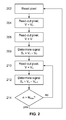
- FIG. 2 schematically shows a flowchart of the method.
- the method starts with a reset of the pixel or all pixels.
- the voltage of the or each pixel is read-out, resulting in a voltage V 0 for the or each pixel.
- the pixel or pixels are read-out for a second time, resulting in a voltage V 1 for the or each pixel.
- the signal S 1 of the or each pixel is determined by subtracting V 0 from V 1
- the pixel or pixels are read-out again, resulting in a voltage V 2
- the signal S 2 is determined by subtracting V 1 from V 2 .
- step 214 the break-off criterion is tested, for example whether the reset occurred a predetermined number of read-outs ago.
- Other criteria for example whether one pixel of the array reached a value at or above its predetermined value (close to the full-well value, for example 0.8 x the full-well capacity) can be used as criterion to reset the whole array of pixels, or the pixels can be reset pixel by pixel when reaching the predetermined value (only applicable if pixels can be reset independently).
- CMOS chip complementary metal-oxide-semiconductor
- TEM Transmission Electron Microscopy
Landscapes
- Engineering & Computer Science (AREA)
- Multimedia (AREA)
- Signal Processing (AREA)
- Solid State Image Pick-Up Elements (AREA)
- Transforming Light Signals Into Electric Signals (AREA)
- Measurement Of Radiation (AREA)
Abstract
The invention relates to a method of using a CMOS chip for direct charged particle counting. To avoid reset noise, it is known to use Correlative Double Sampling: for each signal value the pixel is sampled twice: once (204) directly after reset and once (206) after an integration time. The signal is then determined (208) by subtracting the reset value from the later acquired value, and the pixel is reset again (202). Typically the integration time is chosen sufficiently short that the chance that two particles impinge on one pixel is negligible, thereby enabling event counting.
Although this technique removes reset noise and fixed pattern noise, it also lowers the image rate to half the frame rate, as a pixel needs to be sampled twice for one signal value.
The invention proposes to reset the pixel only after a large number of read-outs. This is based on the insight that typically a large number of events, typically approximately 10, are needed to cause a full pixel. By either resetting after a large number of images, or when one pixel of the image shows a signal above a predetermined value (for example 0.8 x the full-well capacity), the image speed can be almost doubled when compared to the prior art method, using a reset after acquiring a signal.
Description
- The invention relates to a method for acquiring data with an image sensor, the sensor showing a multitude of pixels, the sensor using a reset to bring the pixels to a predetermined state, the method comprising the steps of resetting the voltage of a pixel, reading the voltage of the pixel a first time, resulting in a first read-out value for the pixel, reading the voltage of each pixel a second time, resulting in a second read-out value for the pixel, and determining the difference between the first and the second read-out value of the pixel.
- Such a method is known as Correlative Double Sampling (CDS) and is described in, for example, US patent No.
US6,969,879B2 . The method is used to reduce Fixed Pattern Noise (FPN) and Reset Noise (RN) in, for example, CMOS sensors - In a CMOS sensor a large number of sensitive elements, further referred to as pixels, in the form of photo diodes are arranged in an array. Each of these pixels can be selectively connected to an Analogue-to-Digital Convertor (ADC), and the voltage over the pixel is digitized. The voltage over the pixels is a result of impinging radiation, such as light. It is noted that a CMOS detector is often equipped with a multitude of ADC's, each ADC assigned to a group of pixels.
- The voltage over the pixel after a reset varies from reset to reset. By measuring the voltage over the pixel after a reset, and then reading it out after an integration time, the signal without reset noise can be determined by subtracting the two values from each other.
- By determining the signal of all pixels a frame is read-out. The inverse of the time it takes to read-out all pixels (the whole frame) once is named the frame rate.
- A disadvantage for said CDS method is that for each image all pixels of the sensor need to be read-out twice. This limits the maximum frame-rate with which the sensor can be read-out, and introducing CDS effectively halves the frame rate.
- When using an image sensor for direct particle detection, such as direct electron detection, single particle detection is preferred. Also when using X-rays single event detection is preferred to determine the energy of the X-ray photon, and to distinguish between, for example, two low energy photons from one high energy photon. The occurrence of a single particle or X-ray photon impinging on the detector is then determined by the signal on one or a group of neighboring pixels. The read-out speed of the sensor must be sufficiently high to have a negligible chance that two particles or photons are detected by one pixel between read-outs. The reason is that the signal that is generated by an impinging particle can vary and therefore the difference between e.g. one and two, or three and four particles cannot be determined reliably. For a description of the variation of the signal resulting from one impinging electron, see for example "CMOS Pixel Sensor Response to Low Energy Electrons in Transmission Electron Microscopy", M. Battaglia et al., Nuclear Instruments and Methods in Physics Research Section A: Accelerators, Spectrometers, Detectors and Associated Equipment (2009), Vol. 605, Issue: 3, pages 350-35 (further referred to as Battaglia), specifically
figure 1 . - There is a need for sensors capable to read-out at a high frame rate with a performance of other criteria equal to that of the sensor using CDS.
- It is an object of the invention to provide a method with which a standard image sensor can be operated without loss of performance at a higher frame rate than when using CDS.
- To that end the method according to the invention is characterized by
- ● A subsequent step of reading the voltage of the pixel a third time, resulting in a third read-out value,
- ● between the step of reading the voltage of the pixel a second time and the subsequent step of reading the voltage of the pixel a third time no reset occurs, and
- ● a step of determining a second signal by subtracting the second read-out value from the third read-out value.
- The invention is based on the insight that the capacity of the well (the amount of charge or signal or voltage that can be stored in a pixel) before it overflows, the so-called full-well capacity, is many times larger than the charge resulting from one impinging particle. Typically the full-well capacity corresponds with at least 10 incident particles. By first resetting the pixel, and then reading out the pixel N = 1..Nmax times, and determining the signal per read-out cycles by pair wise subtracting the N-1 value from the Nth value, less resets need to be generated.
- When reading-out M images, the prior art CDS method uses 2xM read-out cycles, while when using the method according to the invention only M+1 read-out cycles are needed. The result is thus a much improved read-out speed.
- The invention is particularly valuable as the method can be performed on a standard, unmodified sensor.
- In a preferred embodiment the invention is used to detect particles, such a neutrons, positrons, electrons, and/or X-rays.
- Such particles are typically detected with a flux that is low compared to the flux of photons when detecting light. The chance that a multitude of events occurs at one pixel is often negligible. Also earlier mentioned particle counting is often preferred. The method according to the invention, offering a higher frame-rate than the prior art method, is then better suited than the prior art method.
- It is noted that the method can also be used when detecting light, but it is unlikely that a fast read-out is required while no overflow of a well occur, or that photon counting is used. However, should this be preferred, for example for photon counting, the method according to the invention can be advantageous.
- When detecting such particles the difference between two subsequently acquired data can be compared to the minimum that an impinging particle would cause. The signal can then be expressed as the number of impinging particles per pixel. As known to the person skilled in the art particle counting results in a better signal-to-noise ratio than analogue processing.
- In a preferred embodiment the detection of a particle is deduced from the (change of) signal of a group of adjacent pixels.
- As known to the skilled person one particle, such as an electron, often causes a signal in several adjacent pixels, see for example Battaglia. In such a case the occurrence of an event and the position of the event may be derived from the signal of several adjacent pixels, for example a group of 4 x 4 pixels.
- In one embodiment the CMOS sensor is reset, either after a predetermined number of read-outs (images) since the last reset, or after detecting that at least one pixel in the series of read-out forming the last frame has a charge above a predetermined value (typically close to the full-well value, for example 0.8 times the full-well value).
- In another embodiment the pixels are reset one at a time, when it is determined that they approach the full-well value. This, however, will probably involve a redesign of the sensor with respect to prior art sensors.
- The method can also be used when reading out CCD's. As known to the skilled person, in a CCD sensor a series of pixels is connected together in such a way, that - triggered by clock signals- the charge of the pixels can shift from one pixel to another. As a result the charge of a series of pixels (either a row or a column) can be shifted serially to the last pixel of the row, the output node. This output node is connected to a charge amplifier. The output node is first reset, and then the charge from one of the row of pixels is shifted in the node, after which the charge amplifier outputs an output signal that is proportional to the charge of the output node. Using CDS for a CCD means that after a reset the remaining charge is determined, and after the shifting the signal is determined by subtracting the voltage measured during reset from the voltage measured when the output node contains the charge of the pixel. The subtraction can be done by a subtraction of the analogue values (for example by storing the charge on a capacitor) or by subtracting values after digitization. By eliminating the reset, gain in time can be achieved.
- In an aspect of the invention a camera for detecting radiation, the camera comprising an image sensor and a controller for controlling reading-out and reset of the sensor, is characterized in that the controller is programmed for performing the method according to the invention.
- The working of the sensor, including reset and read-out cycles, are typically controlled by a controller, either on chip (sharing the silicon of the sensor) or (at least partly) off-chip. How the controller executes the cycles can then be based on the contents of a programmable memory, such as a EEPROM. In that case an existing sensor can be upgraded to perform the method according to the invention..
- The invention is now elucidated using figures, where identical reference numerals refer to corresponding features. To that end:
-
figure 1 schematically shows the voltage on a pixel, and -
figure 2 schematically shows a flowchart of the method -
Figure 1 schematically shows thevoltage 101 on a pixel. At time To the pixel is reset and the voltage on the pixel corresponds tovoltage 102. It is noted that this need not be zero volts, but can be substantially higher, such as shownvalue 103. It is noted that some noise is superimposed on thesignal 101, due to normal noise contributions, but this noise is less than apredetermined value 104 corresponding with one incident particle. At moment T1 it is detected that two subsequent read-outs differ at least avalue 104 of each other, and thus an event (an impinging particle) is detected. Likewise such events are detected at T2, T3 and T4. At T5 it is detected that the signal reaches a value at or abovepredetermined level 105, indicating that the pixel is close to its full-well capacity. Therefore a reset is generated, resulting in anew reset value 106. It is noted that this value need not equal theprevious reset level 103, but may differ slightly. - It is noted that also other reset criteria can be used, such as the number of read-outs or frames that are read, or the recognition that one pixel of the array had a value at or above its predetermined value (close to the full-well value).
- It is mentioned that in the discussed example full-well (or more accurately the predetermined level) is achieved after only 4 events, but that typically the full-well capacity is more than 10 events, and the predetermined level can be chosen to correspond with 8 - 10 events.
-
Figure 2 schematically shows a flowchart of the method.
Instep 202 the method starts with a reset of the pixel or all pixels.
Instep 204 the voltage of the or each pixel is read-out, resulting in a voltage V0 for the or each pixel.
Instep 206 the pixel or pixels are read-out for a second time, resulting in a voltage V1 for the or each pixel.
Instep 208 the signal S1 of the or each pixel is determined by subtracting V0 from V1
Instep 210 the pixel or pixels are read-out again, resulting in a voltage V2
Instep 212 the signal S2 is determined by subtracting V1 from V2.
Instep 214 the break-off criterion is tested, for example whether the reset occurred a predetermined number of read-outs ago. Other criteria, for example whether one pixel of the array reached a value at or above its predetermined value (close to the full-well value, for example 0.8 x the full-well capacity) can be used as criterion to reset the whole array of pixels, or the pixels can be reset pixel by pixel when reaching the predetermined value (only applicable if pixels can be reset independently). - It is noted that the prior art method jumps from
step 208 to 202. If the frame rate of a sensor is N frames/second, then the prior art method achieves image rate of N/2 images per second, while the method according to the invention, using a reset criterion of e.g. a reset after a fixed number of 10 frames, (1-1/10) x N = 0.9 x N images per second, almost twice as fast and almost as fast as the frame rate itself, still offering the performance of the prior art method using CDS on the sensor (chip), all this on the same chip. - The latter implies that the method may also be implemented on an existing apparatus comprising a direct electron sensor, such as a CMOS chip, to detect electrons. Such sensors are known to be used in, for example, electron microscopy, more specifically Transmission Electron Microscopy (TEM). The invention explicitly seeks protection for upgrading existing camera's/apparatuses.
Claims (10)
- Method for acquiring data with an image sensor, the sensor showing a multitude of pixels, the sensor using a reset to bring the pixels to a predetermined state, the method comprising:● A step (202) of resetting the voltage of a pixel;● A step (204) of reading the voltage of the pixel a first time, resulting in a first read-out value for the pixel;● A step (206) of reading the voltage of each pixel a second time, resulting in a second read-out value for the pixel; and● A step (208) of determining a first signal by subtracting the first read-out value from the second read-out value of the pixel;
characterized in● A subsequent step (210) of reading the voltage of the pixel a third time, resulting in a third read-out value,● between the step (206) of reading the voltage of the pixel a second time and the subsequent step (210) of reading the voltage of the pixel a third time no reset occurs, and● a step (212) of determining a second signal by subtracting the second read-out value from the third read-out value. - The method of claim 1 in which after the step (210) of reading the voltage a third time the pixel is read-out multiple times before a reset occurs, resulting in multiple read-out values, and multiple signals are determined by pair-wise taking a read-out value and subtracting from that value the previous read-out value of a pixel.
- The method of claim 1 or claim 2 in which the sensor detects particles from the group of electrons, neutrons, positrons and X-rays.
- The method of claim 3 in which the signal is expressed as the detection of a particle by comparing the signal of one or more pixels to a predetermined threshold value (104), the threshold value corresponding to the minimum signal that a single detected particle causes.
- The method of claim 4 in which the signal of several adjacent pixels is used to be compared with the predetermined value (104)
- The method of any of the preceding claims in which the sensor is a CMOS sensor and each pixel is reset after a predetermined number of read-outs or images (214).
- The method of any of claims 1-5 in which the sensor is a CMOS sensor and the reset is generated when, in the series of read-outs representing the last image, at least one pixel has a read-out value above a predetermined value (105).
- The method of any of claims 1-5 in which the sensor is a CMOS sensor and the reset is generated for each pixel independently when said pixel has a read-out value above a predetermined value (105).
- The method of any of claims 1-5 in which the camera is a CCD sensor and the pixel that is reset is the output node of a series of pixels.
- Camera for detecting radiation, the camera comprising an image sensor and a controller for controlling reading-out and reset of the sensor, characterized in that the controller is programmed for performing any of claims 1, 2, 4, 5, 6, 7, 8, or 9.
Priority Applications (5)
| Application Number | Priority Date | Filing Date | Title |
|---|---|---|---|
| EP11184107.8A EP2579575A1 (en) | 2011-10-06 | 2011-10-06 | Method for acquiring data with an image sensor |
| CN201210370953.8A CN103037175B (en) | 2011-10-06 | 2012-09-29 | For the method obtaining data with imageing sensor |
| JP2012221489A JP6084799B2 (en) | 2011-10-06 | 2012-10-03 | Data acquisition method by image sensor |
| EP12187329.3A EP2579578B1 (en) | 2011-10-06 | 2012-10-05 | Method for acquiring data with an image sensor |
| US13/645,725 US8817148B2 (en) | 2011-10-06 | 2012-10-05 | Method for acquiring data with an image sensor |
Applications Claiming Priority (1)
| Application Number | Priority Date | Filing Date | Title |
|---|---|---|---|
| EP11184107.8A EP2579575A1 (en) | 2011-10-06 | 2011-10-06 | Method for acquiring data with an image sensor |
Publications (1)
| Publication Number | Publication Date |
|---|---|
| EP2579575A1 true EP2579575A1 (en) | 2013-04-10 |
Family
ID=45558429
Family Applications (2)
| Application Number | Title | Priority Date | Filing Date |
|---|---|---|---|
| EP11184107.8A Withdrawn EP2579575A1 (en) | 2011-10-06 | 2011-10-06 | Method for acquiring data with an image sensor |
| EP12187329.3A Active EP2579578B1 (en) | 2011-10-06 | 2012-10-05 | Method for acquiring data with an image sensor |
Family Applications After (1)
| Application Number | Title | Priority Date | Filing Date |
|---|---|---|---|
| EP12187329.3A Active EP2579578B1 (en) | 2011-10-06 | 2012-10-05 | Method for acquiring data with an image sensor |
Country Status (4)
| Country | Link |
|---|---|
| US (1) | US8817148B2 (en) |
| EP (2) | EP2579575A1 (en) |
| JP (1) | JP6084799B2 (en) |
| CN (1) | CN103037175B (en) |
Cited By (2)
| Publication number | Priority date | Publication date | Assignee | Title |
|---|---|---|---|---|
| EP3120897A1 (en) * | 2015-07-22 | 2017-01-25 | Université Pierre et Marie Curie (Paris 6) | Method for downsampling a signal outputted by an asynchronous sensor |
| EP3979626A1 (en) * | 2020-09-30 | 2022-04-06 | FEI Company | Method and system for high speed signal processing |
Families Citing this family (12)
| Publication number | Priority date | Publication date | Assignee | Title |
|---|---|---|---|---|
| FR3012710B1 (en) * | 2013-10-29 | 2017-02-10 | Commissariat Energie Atomique | PROCESS FOR PROCESSING SIGNALS DELIVERED BY PIXELS OF A DETECTOR |
| US9986179B2 (en) * | 2014-09-30 | 2018-05-29 | Qualcomm Incorporated | Sensor architecture using frame-based and event-based hybrid scheme |
| CN105258804B (en) * | 2015-08-17 | 2018-10-26 | 电子科技大学 | The method for sending and receiving Terahertz or infrared focal plane detector array data |
| US10122946B2 (en) | 2015-11-11 | 2018-11-06 | Fei Company | Method for detecting particulate radiation |
| JP6700828B2 (en) | 2016-02-10 | 2020-05-27 | キヤノン株式会社 | Radiation imaging apparatus, driving method thereof and imaging system |
| US10855927B2 (en) | 2017-03-08 | 2020-12-01 | Samsung Electronics Co., Ltd. | Event detecting device including an event signal generator and an output signal generator |
| US10516841B2 (en) * | 2017-03-08 | 2019-12-24 | Samsung Electronics Co., Ltd. | Pixel, pixel driving circuit, and vision sensor including the same |
| US10014158B1 (en) | 2017-05-09 | 2018-07-03 | Fei Company | Innovative image processing in charged particle microscopy |
| CN112399115A (en) * | 2019-08-15 | 2021-02-23 | 天津大学青岛海洋技术研究院 | Working mode for improving dynamic range of small-size pixel image sensor |
| US11694874B2 (en) | 2021-07-13 | 2023-07-04 | Fei Company | Method and system for generating a diffraction image |
| EP4322199A1 (en) | 2022-08-09 | 2024-02-14 | Fei Company | System for sensor protection in electron imaging applications |
| CN118695123B (en) * | 2024-08-26 | 2025-01-03 | 珠海燧景科技有限公司 | Image sensor, image sensing method, imaging system, and program product |
Citations (4)
| Publication number | Priority date | Publication date | Assignee | Title |
|---|---|---|---|---|
| US6969879B2 (en) | 2002-08-22 | 2005-11-29 | Stmicroelectronics Ltd. | Solid state image sensor |
| US20080055440A1 (en) * | 2006-08-29 | 2008-03-06 | Shimon Pertsel | Wide Dynamic Range Image Capturing System Method and Apparatus |
| US20090219387A1 (en) * | 2008-02-28 | 2009-09-03 | Videolq, Inc. | Intelligent high resolution video system |
| EP2312829A2 (en) * | 2009-10-01 | 2011-04-20 | Sony Corporation | Image taking device and camera system |
Family Cites Families (13)
| Publication number | Priority date | Publication date | Assignee | Title |
|---|---|---|---|---|
| JP3631114B2 (en) * | 2000-08-01 | 2005-03-23 | キヤノン株式会社 | Imaging device |
| JP4251811B2 (en) * | 2002-02-07 | 2009-04-08 | 富士通マイクロエレクトロニクス株式会社 | Correlated double sampling circuit and CMOS image sensor having the correlated double sampling circuit |
| JP4468083B2 (en) * | 2003-08-26 | 2010-05-26 | キヤノン株式会社 | Radiographic apparatus and radiographic method |
| US7262411B2 (en) | 2004-12-08 | 2007-08-28 | The Regents Of The University Of California | Direct collection transmission electron microscopy |
| DE602008000086D1 (en) | 2007-06-29 | 2009-09-24 | Fei Co | Method for attaching a sample to a manipulator |
| EP2051280A1 (en) | 2007-10-18 | 2009-04-22 | The Regents of the University of California | Motorized manipulator for positioning a TEM specimen |
| JP5521721B2 (en) * | 2009-08-28 | 2014-06-18 | ソニー株式会社 | Image sensor and camera system |
| EP2381236A1 (en) | 2010-04-23 | 2011-10-26 | Fei Company | Apparatus for preparing a cryogenic TEM specimen |
| EP2383769A1 (en) | 2010-04-28 | 2011-11-02 | Fei Company | Method of using a direct electron detector for a TEM |
| JP5065516B2 (en) | 2010-08-04 | 2012-11-07 | エフ イー アイ カンパニ | Reduction of backscattering in thin electron detectors. |
| EP2461347A1 (en) | 2010-12-06 | 2012-06-06 | Fei Company | Detector system for transmission electron microscope |
| EP2461348A1 (en) | 2010-12-06 | 2012-06-06 | FEI Company | Detector system for use with transmission electron microscope spectroscopy |
| EP2509097A1 (en) | 2011-04-07 | 2012-10-10 | FEI Company | Method of protecting a radiation detector in a charged particle instrument |
-
2011
- 2011-10-06 EP EP11184107.8A patent/EP2579575A1/en not_active Withdrawn
-
2012
- 2012-09-29 CN CN201210370953.8A patent/CN103037175B/en active Active
- 2012-10-03 JP JP2012221489A patent/JP6084799B2/en active Active
- 2012-10-05 US US13/645,725 patent/US8817148B2/en active Active
- 2012-10-05 EP EP12187329.3A patent/EP2579578B1/en active Active
Patent Citations (4)
| Publication number | Priority date | Publication date | Assignee | Title |
|---|---|---|---|---|
| US6969879B2 (en) | 2002-08-22 | 2005-11-29 | Stmicroelectronics Ltd. | Solid state image sensor |
| US20080055440A1 (en) * | 2006-08-29 | 2008-03-06 | Shimon Pertsel | Wide Dynamic Range Image Capturing System Method and Apparatus |
| US20090219387A1 (en) * | 2008-02-28 | 2009-09-03 | Videolq, Inc. | Intelligent high resolution video system |
| EP2312829A2 (en) * | 2009-10-01 | 2011-04-20 | Sony Corporation | Image taking device and camera system |
Non-Patent Citations (1)
| Title |
|---|
| M. BATTAGLIA ET AL.: "CMOS Pixel Sensor Response to Low Energy Electrons in Transmission Electron Microscopy", NUCLEAR INSTRUMENTS AND METHODS IN PHYSICS RESEARCH SECTION A: ACCELERATORS, SPECTROMETERS, DETECTORS AND ASSOCIATED EQUIPMENT, vol. 605, no. 3, 2009, pages 350 - 35, XP026193159, DOI: doi:10.1016/j.nima.2009.03.249 |
Cited By (5)
| Publication number | Priority date | Publication date | Assignee | Title |
|---|---|---|---|---|
| EP3120897A1 (en) * | 2015-07-22 | 2017-01-25 | Université Pierre et Marie Curie (Paris 6) | Method for downsampling a signal outputted by an asynchronous sensor |
| WO2017013065A1 (en) * | 2015-07-22 | 2017-01-26 | Universite Pierre Et Marie Curie (Paris 6) | Method for downsampling a signal outputted by an asynchronous sensor |
| US10500397B2 (en) | 2015-07-22 | 2019-12-10 | Sorbonne Universite | Method for downsampling a signal outputted by an asynchronous sensor |
| EP3979626A1 (en) * | 2020-09-30 | 2022-04-06 | FEI Company | Method and system for high speed signal processing |
| CN114339095A (en) * | 2020-09-30 | 2022-04-12 | Fei 公司 | Method and system for high speed signal processing |
Also Published As
| Publication number | Publication date |
|---|---|
| US20130093931A1 (en) | 2013-04-18 |
| CN103037175A (en) | 2013-04-10 |
| EP2579578B1 (en) | 2014-06-25 |
| CN103037175B (en) | 2016-09-28 |
| EP2579578A1 (en) | 2013-04-10 |
| US8817148B2 (en) | 2014-08-26 |
| JP6084799B2 (en) | 2017-02-22 |
| JP2013085241A (en) | 2013-05-09 |
Similar Documents
| Publication | Publication Date | Title |
|---|---|---|
| US8817148B2 (en) | Method for acquiring data with an image sensor | |
| EP2203762B1 (en) | Particle-counting apparatus with pulse shortening | |
| US10441238B2 (en) | Radiation imaging apparatus, control method thereof, and program | |
| EP2010942B1 (en) | Wireless digital radiography system | |
| US9897707B2 (en) | X-ray detector operable in a mixed photon-counting/analog output mode | |
| US8866094B2 (en) | Radiation detector | |
| US8698922B2 (en) | Black level correction for imaging pixels | |
| JP5324947B2 (en) | Signal processing apparatus and light detection apparatus | |
| WO2015052864A1 (en) | Image-capturing device, radiation detection apparatus, and control method for image-capturing device | |
| US9201150B2 (en) | Suppression of direct detection events in X-ray detectors | |
| CA2690387A1 (en) | Digitizer for a digital imaging system | |
| CA2690382A1 (en) | Antibody formulations | |
| EP2645706A2 (en) | Programmable readout integrated circuit for an ionizing radiation sensor | |
| US11190717B2 (en) | Solid state image sensor, image capturing apparatus, and image capturing method | |
| CN106937063B (en) | Method and system for the analog/digital conversion time for reducing dark signal | |
| US11678076B1 (en) | Systems and methods for binning light detectors | |
| JPH095445A (en) | Radiation image pickup device | |
| Cao et al. | An on-chip hot pixel identification and correction approach in CMOS imagers |
Legal Events
| Date | Code | Title | Description |
|---|---|---|---|
| PUAI | Public reference made under article 153(3) epc to a published international application that has entered the european phase |
Free format text: ORIGINAL CODE: 0009012 |
|
| AK | Designated contracting states |
Kind code of ref document: A1 Designated state(s): AL AT BE BG CH CY CZ DE DK EE ES FI FR GB GR HR HU IE IS IT LI LT LU LV MC MK MT NL NO PL PT RO RS SE SI SK SM TR |
|
| AX | Request for extension of the european patent |
Extension state: BA ME |
|
| STAA | Information on the status of an ep patent application or granted ep patent |
Free format text: STATUS: THE APPLICATION IS DEEMED TO BE WITHDRAWN |
|
| 18D | Application deemed to be withdrawn |
Effective date: 20131011 |