EP2579434A2 - Rectifier with power factor correction - Google Patents
Rectifier with power factor correction Download PDFInfo
- Publication number
- EP2579434A2 EP2579434A2 EP12187453.1A EP12187453A EP2579434A2 EP 2579434 A2 EP2579434 A2 EP 2579434A2 EP 12187453 A EP12187453 A EP 12187453A EP 2579434 A2 EP2579434 A2 EP 2579434A2
- Authority
- EP
- European Patent Office
- Prior art keywords
- rectifier
- current
- switching
- alternating
- direct
- Prior art date
- Legal status (The legal status is an assumption and is not a legal conclusion. Google has not performed a legal analysis and makes no representation as to the accuracy of the status listed.)
- Withdrawn
Links
Images
Classifications
-
- H—ELECTRICITY
- H02—GENERATION; CONVERSION OR DISTRIBUTION OF ELECTRIC POWER
- H02M—APPARATUS FOR CONVERSION BETWEEN AC AND AC, BETWEEN AC AND DC, OR BETWEEN DC AND DC, AND FOR USE WITH MAINS OR SIMILAR POWER SUPPLY SYSTEMS; CONVERSION OF DC OR AC INPUT POWER INTO SURGE OUTPUT POWER; CONTROL OR REGULATION THEREOF
- H02M1/00—Details of apparatus for conversion
- H02M1/0083—Converters characterised by their input or output configuration
- H02M1/0085—Partially controlled bridges
-
- H—ELECTRICITY
- H02—GENERATION; CONVERSION OR DISTRIBUTION OF ELECTRIC POWER
- H02M—APPARATUS FOR CONVERSION BETWEEN AC AND AC, BETWEEN AC AND DC, OR BETWEEN DC AND DC, AND FOR USE WITH MAINS OR SIMILAR POWER SUPPLY SYSTEMS; CONVERSION OF DC OR AC INPUT POWER INTO SURGE OUTPUT POWER; CONTROL OR REGULATION THEREOF
- H02M1/00—Details of apparatus for conversion
- H02M1/42—Circuits or arrangements for compensating for or adjusting power factor in converters or inverters
- H02M1/4208—Arrangements for improving power factor of AC input
- H02M1/4225—Arrangements for improving power factor of AC input using a non-isolated boost converter
-
- H—ELECTRICITY
- H02—GENERATION; CONVERSION OR DISTRIBUTION OF ELECTRIC POWER
- H02M—APPARATUS FOR CONVERSION BETWEEN AC AND AC, BETWEEN AC AND DC, OR BETWEEN DC AND DC, AND FOR USE WITH MAINS OR SIMILAR POWER SUPPLY SYSTEMS; CONVERSION OF DC OR AC INPUT POWER INTO SURGE OUTPUT POWER; CONTROL OR REGULATION THEREOF
- H02M7/00—Conversion of AC power input into DC power output; Conversion of DC power input into AC power output
- H02M7/02—Conversion of AC power input into DC power output without possibility of reversal
- H02M7/04—Conversion of AC power input into DC power output without possibility of reversal by static converters
- H02M7/12—Conversion of AC power input into DC power output without possibility of reversal by static converters using discharge tubes with control electrode or semiconductor devices with control electrode
- H02M7/21—Conversion of AC power input into DC power output without possibility of reversal by static converters using discharge tubes with control electrode or semiconductor devices with control electrode using devices of a triode or transistor type requiring continuous application of a control signal
- H02M7/217—Conversion of AC power input into DC power output without possibility of reversal by static converters using discharge tubes with control electrode or semiconductor devices with control electrode using devices of a triode or transistor type requiring continuous application of a control signal using semiconductor devices only
- H02M7/219—Conversion of AC power input into DC power output without possibility of reversal by static converters using discharge tubes with control electrode or semiconductor devices with control electrode using devices of a triode or transistor type requiring continuous application of a control signal using semiconductor devices only in a bridge configuration
-
- H—ELECTRICITY
- H02—GENERATION; CONVERSION OR DISTRIBUTION OF ELECTRIC POWER
- H02M—APPARATUS FOR CONVERSION BETWEEN AC AND AC, BETWEEN AC AND DC, OR BETWEEN DC AND DC, AND FOR USE WITH MAINS OR SIMILAR POWER SUPPLY SYSTEMS; CONVERSION OF DC OR AC INPUT POWER INTO SURGE OUTPUT POWER; CONTROL OR REGULATION THEREOF
- H02M1/00—Details of apparatus for conversion
- H02M1/0048—Circuits or arrangements for reducing losses
- H02M1/0054—Transistor switching losses
-
- Y—GENERAL TAGGING OF NEW TECHNOLOGICAL DEVELOPMENTS; GENERAL TAGGING OF CROSS-SECTIONAL TECHNOLOGIES SPANNING OVER SEVERAL SECTIONS OF THE IPC; TECHNICAL SUBJECTS COVERED BY FORMER USPC CROSS-REFERENCE ART COLLECTIONS [XRACs] AND DIGESTS
- Y02—TECHNOLOGIES OR APPLICATIONS FOR MITIGATION OR ADAPTATION AGAINST CLIMATE CHANGE
- Y02B—CLIMATE CHANGE MITIGATION TECHNOLOGIES RELATED TO BUILDINGS, e.g. HOUSING, HOUSE APPLIANCES OR RELATED END-USER APPLICATIONS
- Y02B70/00—Technologies for an efficient end-user side electric power management and consumption
- Y02B70/10—Technologies improving the efficiency by using switched-mode power supplies [SMPS], i.e. efficient power electronics conversion e.g. power factor correction or reduction of losses in power supplies or efficient standby modes
Definitions
- the present invention relates to an alternating-current/direct-current converter.
- Japanese Unexamined Patent Application Publication No. 2008-295248 discloses a conventional alternating-current/direct-current (AC/DC) converter.
- AC/DC alternating-current/direct-current
- a rectification step-down chopper circuit and a boost chopper circuit are arranged in series to constitute a power-factor improving converter to improve power factor.
- an alternating-current/direct-current converter includes a rectifier, a reactor, a capacitor, and a switching rectifier.
- the rectifier is configured to rectify alternating-current voltage output from an alternating-current power source, thereby converting the alternating-current voltage into direct-current voltage, and to output the direct-current voltage.
- the capacitor includes terminals.
- the switching rectifier is coupled to the alternating-current power source and switchable to output the direct-current voltage to the capacitor.
- the reactor when the switching rectifier is in on state, the reactor may be configured to accumulate energy from the alternating-current power source. When the switching rectifier is in off state, the reactor may be configured to release energy. The alternating-current voltage may be boosted and the boosted voltage may be output to between the terminals of the capacitor.
- the rectifier may include a first rectifier and a second rectifier.
- the first rectifier may be disposed between the alternating-current power source and the reactor.
- the second rectifier may be disposed between the alternating-current power source and the capacitor.
- the switching rectifier and the first rectifier When the switching rectifier is in on state, the switching rectifier and the first rectifier may be configured to form a circuit to accumulate energy in the reactor.
- the switching rectifier is in off state, the first rectifier and the second rectifier may be configured to form a circuit to release energy from the reactor to the capacitor.
- the second rectifier may include a switching element.
- the first rectifier may be configured to be comprised in a negative side of a direct-current output of the rectifier.
- the second rectifier may be configured to be comprised in a positive side of the direct-current output of the rectifier.
- the first rectifier may be configured to be comprised in a positive side of a direct-current output of the rectifier.
- the second rectifier may be configured to be comprised in a negative side of the direct-current output of the rectifier.
- the rectifier may include a first rectifier element, a second rectifier element, a first switching element, and a second switching element.
- the first switching element may be coupled to the first rectifier element at a first common coupling point.
- the second switching element may be coupled to the second rectifier element at a second common coupling point.
- the switching rectifier may include a third switching element and a fourth switching element.
- the first switching element, the second switching element, the third switching element, and the fourth switching element each may include a reverse-blocking insulated gate bipolar transistor.
- the first switching element, the second switching element, the third switching element, and the fourth switching element each may include a series assembly of a rectifier element and a switching element without a reverse-blocking function.
- the rectifier may include a single rectifier element without a switching function.
- FIGs. 1 to 5A and 5B An alternating-current/direct-current converter according to any of the embodiments of the present invention will be described by referring to FIGs. 1 to 5A and 5B . It will be appreciated that the embodiments and the accompanying drawings are not intended to limit the present invention, but that the present invention is intended to embrace all such alternatives, modifications, equivalents and variations that are within the spirit and scope of the present invention.
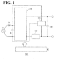
- FIG. 1 is a schematic diagram illustrating an alternating-current/direct-current (AC/DC) converter 100 according to any of the embodiments of the present invention.
- the AC/DC converter 100 converts alternating-current (AC) voltage (V ac ) output from an AC power source A into direct-current (DC) voltage (V dc ).
- the AC/DC converter 100 includes a rectifier 150, a reactor 120, a capacitor 160, and a switching rectifier 110.
- the rectifier 150 rectifies AC voltage and outputs DC.
- the switching rectifier 110 is coupled to the AC power source A. By the switching operation of the switching rectifier 110, DC voltage is output to between the terminals of the capacitor 160.
- the AC/DC converter 100 includes an AC capacitor B and an AC reactor D.
- the AC power source A supplies power to the AC/DC converter 100 through a low-frequency filter circuit formed by the AC capacitor B and the AC reactor D.
- the AC/DC converter 100 further includes a control circuit E.
- the control circuit E compares the voltage of the AC power source A and the DC voltage with one another, and based on the comparison, controls the switching rectifier 110 to turn into on state or off state.
- the switching rectifier 110 is switchable between on state and off state.
- the reactor 120 is coupled to an output of the rectifier 150. Further, the reactor 120 boosts the AC voltage according to the switching between on state and off state of the switching rectifier 110.
- the first rectifier 130 included in the rectifier 150 is disposed between the AC power source A and the reactor 120 and the second rectifier 140 also included in the rectifier 150 is disposed between the AC power source A and a DC capacitor.
- the capacitor 160 is a DC capacitor.
- the first rectifier 130 and the second rectifier 140 are illustrated in FIG. 2 and later drawings.
- the first rectifier 130 may constitute the positive side of the DC output of the rectifier 150, while the second rectifier 140 may constitute the negative side of the DC output of the rectifier 150.
- the first rectifier 130 may constitute the negative side of the DC output of the rectifier 150, while the second rectifier 140 may constitute the positive side of the DC output of the rectifier 150.
- the switching rectifier 110 and the rectifier 150 form a circuit to accumulate energy in the reactor 120.
- the control circuit E controls the switching rectifier 110 to turn into off state the rectifier 150 forms a circuit to release energy from the reactor 120 to the capacitor 160.
- the AC voltage is boosted and the boosted voltage is output to between the terminals of the capacitor 160.
- the control circuit E controls the switching rectifier 110 to turn into on state the switching rectifier 110 and the first rectifier 130 form a circuit to accumulate energy in the reactor 120.
- the first rectifier 130 and the second rectifier 140 form a circuit to release energy from the reactor 120 to the capacitor 160.
- the reactor 120 boosts the AC voltage according to the switching between on state and off state of the switching rectifier 110.
- the AC/DC converter 100 may also function as a step-down circuit, which is implemented by the control circuit E controlling the switching rectifier 110 and the rectifier 150. This will be described in detail in embodiment 1 and embodiment 2 by referring to FIGs. 2 to 5A and 5B .
- the switching rectifier 110 when the switching rectifier 110 is turned into on state, the switching rectifier 110 and the first rectifier 130 form a rectifier circuit.
- the switching rectifier 110 When the switching rectifier 110 is turned into off state, the first rectifier 130 and the second rectifier 140 form a rectifier circuit.
- a total of two semiconductor elements exist along the path through which the current flows, namely the switching rectifier 110 and the first rectifier 130, or the first rectifier 130 and the second rectifier 140.
- the AC/DC converter 100 reduces the number of the semiconductor elements that exist along the path through which the current flows, thereby reducing the conduction loss, as compared with the above-described conventional AC/DC converter, where a total of three semiconductor elements exist along the path through which the current flows.
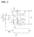
- FIG. 2 is a schematic diagram illustrating an AC/DC converter 200 according to embodiment 1.
- the AC/DC converter 200 converts AC voltage (V ac ) output from the AC power source A into DC voltage (V dc ).
- the AC/DC converter 200 includes the switching rectifier 110, the reactor 120, the capacitor 160, the first rectifier 130, and the second rectifier 140.
- the AC/DC converter 200 includes the AC capacitor B and the AC reactor D.
- the AC/DC converter 200 further includes the control circuit E.
- the control circuit E acquires an output from a detection circuit to detect the AC voltage V ac , and acquires, from an external command tool (not shown) or the like, a DC voltage command value V dc-ref as a command of the DC output voltage.
- the DC voltage command value V dc-ref may be set in the control circuit E.
- the AC power source A includes a terminal A1 and a terminal A2.
- the AC/DC converter 200 is one specific example of the AC/DC converter 100.
- the elements having same functions as in the AC/DC converter 100 are designated the same reference numerals and will not be elaborated here.
- the reactor 120 and the switching rectifier 110 are configured such that the current flowing through the reactor 120 flows to the negative side of the output of the rectifier 150 when the switching rectifier 110 is in on state.
- the first rectifier 130 constitutes the negative side of the DC output of the rectifier 150
- the second rectifier 140 constitutes the positive side of the DC output of the rectifier 150.
- the reactor 120, the first rectifier 130, and the switching rectifier 110 are coupled to each other so that the current flowing through the reactor 120 flows to the first rectifier 130 when the switching rectifier 110 is in on state.
- the first rectifier 130 includes a first rectifier element 131 and a second rectifier element 132.
- the second rectifier 140 includes a first switching element 141 and a second switching element 142.
- the first switching element 141 and the second rectifier element 132 are coupled to one another at a first common coupling point P1, while the second switching element 142 and the first rectifier element 131 are coupled to one another at a second common coupling point P2.
- the switching rectifier 110 includes a third switching element 111 and a fourth switching element 112.
- the first switching element 141, the second switching element 142, the third switching element 111, and the fourth switching element 112 are reverse-blocking insulated gate bipolar transistors (IGBTs).
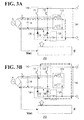
- FIGs. 3A and 3B are schematic diagram illustrating a current flow in the AC/DC converter 200 according to embodiment 1.
- FIG. 3A illustrates a current flow in the AC/DC converter 200 with the switching rectifier 110 in on state.
- FIG. 3B illustrates a current flow in the AC/DC converter 200 with the switching rectifier 110 in off state.
- a boost chopper operation of the AC/DC converter 200 will be described below.
- the control circuit E calculates an absolute value
- the AC/DC converter 200 performs its boost chopper operation when the relationship "
- the control circuit E transmits a gate drive signal to the reverse-blocking IGBT 141 and the reverse-blocking IGBT 142 so that the first switching element 141 (reverse-blocking IGBT 141) and the second switching element 142 (reverse-blocking IGBT 142) of the second rectifier 140 are kept on state.
- the control circuit E then pulse-drives the third switching element 111 (reverse-blocking IGBT 111) and the fourth switching element 112 (reverse-blocking IGBT 112) of the switching rectifier 110 simultaneously, thereby turning the AC/DC converter 200 into boost chopper operation.
- the control circuit E transmits a gate drive signal to the third switching element 111 and the fourth switching element 112, and drives the third switching element 111 and the fourth switching element 112 between on state and off state.
- a current flow in the AC/DC converter 200 will be described by referring to FIG. 3A .
- the switching rectifier 110 When the switching rectifier 110 is in on state, the current flowing from the AC power source A flows through the reverse-blocking IGBT 111, the reactor 120, and the first rectifier element 131 in this order.
- the switching rectifier 110 and the first rectifier 130 form a circuit to accumulate energy in the reactor 120.
- a step-down chopper operation of the AC/DC converter 200 will be described below.
- the AC/DC converter 200 performs its step-down chopper operation when the relationship "
- the control circuit E keeps the reverse-blocking IGBT 111 and the reverse-blocking IGBT 112 of the switching rectifier 110 continuously in off state. When V ac ⁇ 0, the control circuit E turns the reverse-blocking IGBT 142 into on state and pulse-drives the reverse-blocking IGBT 141, thereby turning the AC/DC converter 200 into step-down chopper operation.
- the control circuit E controls the gate of the reverse-blocking IGBT 141 between on state and off state.
- the reverse-blocking IGBT 141 functions as a switching element, while the reverse-blocking IGBT 142 functions as a free wheel diode.
- the control circuit E turns the reverse-blocking IGBT 141 into on state and pulse-drives the reverse-blocking IGBT 142, thereby turning the AC/DC converter 200 into step-down chopper operation.
- the reverse-blocking IGBT 142 functions as a switching element, while the reverse-blocking IGBT 141 functions as a free wheel diode.
- the control circuit E may detect a current I dc through the reactor 120 and perform the pulse driving such that the waveform of I dc has a similar shape with that of
- the control circuit E may also change the peak value of the waveform of I dc to control the DC voltage V dc to match the DC voltage command value V dc - ref .
- the DC voltage command value V dc-ref is variable from zero to equal to or more than the peak voltage of
- the circuit having the step-down circuit function and the circuit having the booster circuit function are switched to and from one another, and the DC voltage V dc follows the varying DC voltage command value V dc-ref by detecting the AC voltage V ac without regard to an instantaneous value of the AC voltage V ac .
- the switching rectifier 110 when the switching rectifier 110 is turned into on state, the switching rectifier 110 and the first rectifier 130 form a rectifier circuit, while when the switching rectifier 110 is turned into off state, the first rectifier 130 and the second rectifier 140 form a rectifier circuit.
- the AC/DC converter 200 reduces the number of the semiconductor elements that exist along the path through which the current flows, thereby reducing the conduction loss, as compared with the above-described conventional AC/DC converter, where a total of three semiconductor elements exist along the path through which the current flows.
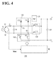
- FIG. 4 is a schematic diagram illustrating an AC/DC converter 300 according to embodiment 2.
- the AC/DC converter 300 converts AC voltage (V ac ) output from the AC power source A into DC voltage (V dc ).
- the AC/DC converter 300 includes the switching rectifier 110, the reactor 120, the first rectifier 130, the second rectifier 140, the AC capacitor B, the capacitor 160, and the AC reactor D. Similar to embodiment 1, the AC/DC converter 300 further includes the control circuit E and acquires a detected value of the AC voltage V ac and the DC voltage command value V dc-ref .
- the AC power source A includes the terminal A1 and the terminal A2.
- the AC/DC converter 300 is one specific example of the AC/DC converter 100.
- the elements having same functions as in the AC/DC converter 100 are designated the same reference numerals and will not be elaborated here.
- the AC/DC converter 300 is different from the AC/DC converter 200 according to embodiment 1 in that the reactor 120 is shifted to the positive side of the rectifier circuit, and accordingly, the arrangement of the reverse-blocking IGBTs and rectifier elements is also changed.
- the reactor 120 and the switching rectifier 110 are configured such that the current flowing through the reactor 120 flows to the positive side of the output of the rectifier 150 when the switching rectifier 110 is in on state.
- the first rectifier 130 constitutes the positive side of the DC output of the rectifier 150
- the second rectifier 140 constitutes the negative side of the DC output of the rectifier 150.
- the reactor 120, the first rectifier 130, and the switching rectifier 110 are disposed such that the current flowing through the reactor 120 flows to the first rectifier 130 when the switching rectifier 110 is in on state.
- the first rectifier 130 includes the first rectifier element 131 and the second rectifier element 132.
- the second rectifier 140 includes the first switching element 141 and the second switching element 142.
- the first switching element 141 and the second rectifier element 132 are coupled to one another at the first common coupling point P1, while the second switching element 142 and the first rectifier element 131 are coupled to one another at the second common coupling point P2.
- the switching rectifier 110 includes the third switching element 111 and the fourth switching element 112.
- the first switching element 141, the second switching element 142, the third switching element 111, and the fourth switching element 112 are reverse-blocking IGBTs.
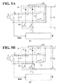
- FIGs. 5A and 5B are schematic diagram illustrating a current flow in the AC/DC converter 300 according to embodiment 2.
- FIG. 5A illustrates a current flow with the switching rectifier 110 in on state in the AC/DC converter 300.
- FIG. 5B illustrates a current flow with the switching rectifier 110 in off state in the AC/DC converter 300.
- a boost chopper operation of the AC/DC converter 300 will be described. Similar to embodiment 1, the control circuit E performs the boost chopper operation when the relationship "
- the control circuit E transmits a gate drive signal to the reverse-blocking IGBT 141 and the reverse-blocking IGBT 142 so that the first switching element 141 (reverse-blocking IGBT 141) and the second switching element 142 (reverse-blocking IGBT 142) of the second rectifier 140 are continuously kept on state.
- the control circuit E then pulse-drives the third switching element 111 (reverse-blocking IGBT 111) and the fourth switching element 112 (reverse-blocking IGBT 112) of the switching rectifier 110 simultaneously, thereby turning the AC/DC converter 300 into boost chopper operation.
- the time for which the switching rectifier 110 is in on state and the time for which the switching rectifier 110 is in off state are determined by a similar method to the method in embodiment 1.
- a current flow in the AC/DC converter 300 will be described by referring to FIG. 5A .
- the switching rectifier 110 When the switching rectifier 110 is in on state, the current flowing from the AC power source A flows through the second rectifier element 132, the reactor 120, and the reverse-blocking IGBT 112 in this order.
- the switching rectifier 110 and the first rectifier 130 form a circuit to accumulate energy in the reactor 120.
- a step-down chopper operation of the AC/DC converter 300 will be described below.
- the AC/DC converter 300 performs its step-down chopper operation when the relationship "
- the control circuit E keeps the reverse-blocking IGBT 111 and the reverse-blocking IGBT 112 of the switching rectifier 110 continuously in off state. When V ac ⁇ 0, the control circuit E keeps the reverse-blocking IGBT 141 continuously in on state and pulse-drives the reverse-blocking IGBT 142, thereby turning the AC/DC converter 300 into step-down chopper operation.
- the control circuit E controls the gate of the reverse-blocking IGBT 142 between on state and off state.
- the reverse-blocking IGBT 142 functions as a switching element, while the reverse-blocking IGBT 141 functions as a free wheel diode.
- the control circuit E turns the reverse-blocking IGBT 142 into on state and pulse-drives the reverse-blocking IGBT 141, thereby turning it into step-down chopper operation.
- the reverse-blocking IGBT 141 functions as a switching element
- the reverse-blocking IGBT 142 functions as a free wheel diode.
- the control circuit E may detect current I dc through the reactor 120 and perform the pulse driving such that the waveform of I dc has a similar shape with that of
- the control circuit E may also change the peak value of the waveform of I dc to control the DC voltage V dc to match the DC voltage command value V dc-ref .
- the DC voltage command value V dc-ref is variable from zero to equal to or more than the peak voltage of
- the switching rectifier 110 when the switching rectifier 110 is turned into on state, the switching rectifier 110 and the first rectifier 130 form a rectifier circuit, while when the switching rectifier 110 is turned into off state, the first rectifier 130 and the second rectifier 140 form a rectifier circuit.
- the AC/DC converter 300 reduces the number of the semiconductor elements that exist along the path through which the current flows, thereby reducing the conduction loss, as compared with the above-described conventional AC/DC converter, where a total of three semiconductor elements exist along the path through which the current flows.
- the rectifier 150 may be made up of only a rectifier element.
- the first rectifier 130 and the second rectifier 140 each may also be made up of only a rectifier element.
- the AC/DC converter according to any of the embodiments has the half-wave rectification function instead of the full-wave rectification function, and has only the boosting function.
- the first switching element 141, the second switching element 142, the third switching element 111, and the fourth switching element 112 will not be limited to reverse-blocking IGBTs.
- the first switching element 141, the second switching element 142, the third switching element 111, and the fourth switching element 112 each may also be other than a reverse-blocking IGBT, examples including, but not limited to, a series assembly of a rectifier element and a switching element without the reverse-blocking function (for example, MOSFET and IGBT without the reverse-blocking function).
- MOSFET as the switching element ensures higher switching frequencies than the use of reverse-blocking IGBT, and reduces the reactor value and shape of the reactor 120.
- the embodiments of the present invention will find applications in AC/DC converters to convert AC voltage output from an AC power source into DC voltage.
Landscapes
- Engineering & Computer Science (AREA)
- Power Engineering (AREA)
- Rectifiers (AREA)
- Dc-Dc Converters (AREA)
Abstract
Description
- The present invention relates to an alternating-current/direct-current converter.
- Japanese Unexamined Patent Application Publication No.
2008-295248 - The contents of Japanese Unexamined Patent Application Publication No.
2008-295248 - In the AC/DC converter recited in Japanese Unexamined Patent Application Publication No.
2008-295248 - It is an object of the present invention to provide an alternating-current/direct-current converter that reduces the number of semiconductor elements along the path in a circuit through which current flows, thereby reducing the conduction loss.
- According to one aspect of the present invention, an alternating-current/direct-current converter includes a rectifier, a reactor, a capacitor, and a switching rectifier. The rectifier is configured to rectify alternating-current voltage output from an alternating-current power source, thereby converting the alternating-current voltage into direct-current voltage, and to output the direct-current voltage. The capacitor includes terminals. The switching rectifier is coupled to the alternating-current power source and switchable to output the direct-current voltage to the capacitor.
- In the one aspect of the present invention, when the switching rectifier is in on state, the reactor may be configured to accumulate energy from the alternating-current power source. When the switching rectifier is in off state, the reactor may be configured to release energy. The alternating-current voltage may be boosted and the boosted voltage may be output to between the terminals of the capacitor.
- In the one aspect of the present invention, the rectifier may include a first rectifier and a second rectifier. The first rectifier may be disposed between the alternating-current power source and the reactor. The second rectifier may be disposed between the alternating-current power source and the capacitor. When the switching rectifier is in on state, the switching rectifier and the first rectifier may be configured to form a circuit to accumulate energy in the reactor. When the switching rectifier is in off state, the first rectifier and the second rectifier may be configured to form a circuit to release energy from the reactor to the capacitor.
- In the one aspect of the present invention, the second rectifier may include a switching element.
- In the one aspect of the present invention, the first rectifier may be configured to be comprised in a negative side of a direct-current output of the rectifier. The second rectifier may be configured to be comprised in a positive side of the direct-current output of the rectifier.
- In the one aspect of the present invention, the first rectifier may be configured to be comprised in a positive side of a direct-current output of the rectifier. The second rectifier may be configured to be comprised in a negative side of the direct-current output of the rectifier.
- In the one aspect of the present invention, the rectifier may include a first rectifier element, a second rectifier element, a first switching element, and a second switching element. The first switching element may be coupled to the first rectifier element at a first common coupling point. The second switching element may be coupled to the second rectifier element at a second common coupling point. The switching rectifier may include a third switching element and a fourth switching element.
- In the one aspect of the present invention, the first switching element, the second switching element, the third switching element, and the fourth switching element each may include a reverse-blocking insulated gate bipolar transistor.
- In the one aspect of the present invention, the first switching element, the second switching element, the third switching element, and the fourth switching element each may include a series assembly of a rectifier element and a switching element without a reverse-blocking function.
- In the one aspect of the present invention, the rectifier may include a single rectifier element without a switching function.
- A more complete appreciation of the invention and many of the attendant advantages thereof will be readily obtained as the same becomes better understood by reference to the following detailed description when considered in connection with the accompanying drawings, wherein:
-
FIG. 1 is a schematic diagram illustrating an alternating-current/direct-current converter according to any of the embodiments of the present invention; -
FIG. 2 is a schematic diagram illustrating an alternating-current/direct-current converter according to embodiment 1; -
FIGs. 3A and 3B each are a schematic diagram illustrating a current flow in the alternating-current/direct-current converter according to embodiment 1; -
FIG. 4 is a schematic diagram illustrating an alternating-current/direct-current converter according to embodiment 2; and -
FIGs. 5A and 5B each are a schematic diagram illustrating a current flow in the alternating-current/direct-current converter according to embodiment 2. - An alternating-current/direct-current converter according to any of the embodiments of the present invention will be described by referring to
FIGs. 1 to 5A and 5B . It will be appreciated that the embodiments and the accompanying drawings are not intended to limit the present invention, but that the present invention is intended to embrace all such alternatives, modifications, equivalents and variations that are within the spirit and scope of the present invention. -
FIG. 1 is a schematic diagram illustrating an alternating-current/direct-current (AC/DC)converter 100 according to any of the embodiments of the present invention. The AC/DC converter 100 converts alternating-current (AC) voltage (Vac) output from an AC power source A into direct-current (DC) voltage (Vdc). The AC/DC converter 100 includes arectifier 150, areactor 120, acapacitor 160, and aswitching rectifier 110. Therectifier 150 rectifies AC voltage and outputs DC. Theswitching rectifier 110 is coupled to the AC power source A. By the switching operation of theswitching rectifier 110, DC voltage is output to between the terminals of thecapacitor 160. The AC/DC converter 100 includes an AC capacitor B and an AC reactor D. The AC power source A supplies power to the AC/DC converter 100 through a low-frequency filter circuit formed by the AC capacitor B and the AC reactor D. - The AC/
DC converter 100 further includes a control circuit E. The control circuit E compares the voltage of the AC power source A and the DC voltage with one another, and based on the comparison, controls theswitching rectifier 110 to turn into on state or off state. - For example, the
switching rectifier 110 is switchable between on state and off state. Thereactor 120 is coupled to an output of therectifier 150. Further, thereactor 120 boosts the AC voltage according to the switching between on state and off state of theswitching rectifier 110. For example, thefirst rectifier 130 included in therectifier 150 is disposed between the AC power source A and thereactor 120 and thesecond rectifier 140 also included in therectifier 150 is disposed between the AC power source A and a DC capacitor. For example, thecapacitor 160 is a DC capacitor. Thefirst rectifier 130 and thesecond rectifier 140 are illustrated inFIG. 2 and later drawings. - In the AC/
DC converter 100, thefirst rectifier 130 may constitute the positive side of the DC output of therectifier 150, while thesecond rectifier 140 may constitute the negative side of the DC output of therectifier 150. Alternatively, in the AC/DC converter 100, thefirst rectifier 130 may constitute the negative side of the DC output of therectifier 150, while thesecond rectifier 140 may constitute the positive side of the DC output of therectifier 150. - When the control circuit E controls the
switching rectifier 110 to turn into on state, theswitching rectifier 110 and therectifier 150 form a circuit to accumulate energy in thereactor 120. When the control circuit E controls the switchingrectifier 110 to turn into off state, therectifier 150 forms a circuit to release energy from thereactor 120 to thecapacitor 160. As a result, the AC voltage is boosted and the boosted voltage is output to between the terminals of thecapacitor 160. One specific example is that when the control circuit E controls the switchingrectifier 110 to turn into on state, the switchingrectifier 110 and thefirst rectifier 130 form a circuit to accumulate energy in thereactor 120. When the control circuit E controls the switchingrectifier 110 to turn into off state, thefirst rectifier 130 and thesecond rectifier 140 form a circuit to release energy from thereactor 120 to thecapacitor 160. - The
reactor 120 boosts the AC voltage according to the switching between on state and off state of the switchingrectifier 110. In addition to functioning as a booster circuit, the AC/DC converter 100 may also function as a step-down circuit, which is implemented by the control circuit E controlling the switchingrectifier 110 and therectifier 150. This will be described in detail in embodiment 1 and embodiment 2 by referring toFIGs. 2 to 5A and 5B . - In the AC/
DC converter 100, when the switchingrectifier 110 is turned into on state, the switchingrectifier 110 and thefirst rectifier 130 form a rectifier circuit. When the switchingrectifier 110 is turned into off state, thefirst rectifier 130 and thesecond rectifier 140 form a rectifier circuit. Thus, regardless of whether the switchingrectifier 110 is in on state or off state, a total of two semiconductor elements exist along the path through which the current flows, namely the switchingrectifier 110 and thefirst rectifier 130, or thefirst rectifier 130 and thesecond rectifier 140. Thus, the AC/DC converter 100 reduces the number of the semiconductor elements that exist along the path through which the current flows, thereby reducing the conduction loss, as compared with the above-described conventional AC/DC converter, where a total of three semiconductor elements exist along the path through which the current flows. -
FIG. 2 is a schematic diagram illustrating an AC/DC converter 200 according to embodiment 1. The AC/DC converter 200 converts AC voltage (Vac) output from the AC power source A into DC voltage (Vdc). The AC/DC converter 200 includes the switchingrectifier 110, thereactor 120, thecapacitor 160, thefirst rectifier 130, and thesecond rectifier 140. The AC/DC converter 200 includes the AC capacitor B and the AC reactor D. The AC/DC converter 200 further includes the control circuit E. The control circuit E acquires an output from a detection circuit to detect the AC voltage Vac, and acquires, from an external command tool (not shown) or the like, a DC voltage command value Vdc-ref as a command of the DC output voltage. The DC voltage command value Vdc-ref may be set in the control circuit E. - The AC power source A includes a terminal A1 and a terminal A2. In embodiment 1, Vac is defined as "Vac = the potential of the terminal A1 - the potential of the terminal A2". That is, "Vac ≥ 0" denotes that the potential of the terminal A1 is equal to or more than the potential of the terminal A2, and "Vac < 0" denotes that the potential of the terminal A1 is lower than the potential of the terminal A2.
- The AC/
DC converter 200 is one specific example of the AC/DC converter 100. In the AC/DC converter 200, the elements having same functions as in the AC/DC converter 100 are designated the same reference numerals and will not be elaborated here. - In the AC/
DC converter 200, thereactor 120 and the switchingrectifier 110 are configured such that the current flowing through thereactor 120 flows to the negative side of the output of therectifier 150 when the switchingrectifier 110 is in on state. Specifically, as shown inFIG. 2 , thefirst rectifier 130 constitutes the negative side of the DC output of therectifier 150, while thesecond rectifier 140 constitutes the positive side of the DC output of therectifier 150. Thereactor 120, thefirst rectifier 130, and the switchingrectifier 110 are coupled to each other so that the current flowing through thereactor 120 flows to thefirst rectifier 130 when the switchingrectifier 110 is in on state. - The
first rectifier 130 includes afirst rectifier element 131 and asecond rectifier element 132. Thesecond rectifier 140 includes afirst switching element 141 and asecond switching element 142. Thefirst switching element 141 and thesecond rectifier element 132 are coupled to one another at a first common coupling point P1, while thesecond switching element 142 and thefirst rectifier element 131 are coupled to one another at a second common coupling point P2. The switchingrectifier 110 includes athird switching element 111 and afourth switching element 112. - The
first switching element 141, thesecond switching element 142, thethird switching element 111, and thefourth switching element 112 are reverse-blocking insulated gate bipolar transistors (IGBTs). - Each of
FIGs. 3A and 3B is a schematic diagram illustrating a current flow in the AC/DC converter 200 according to embodiment 1.FIG. 3A illustrates a current flow in the AC/DC converter 200 with the switchingrectifier 110 in on state.FIG. 3B illustrates a current flow in the AC/DC converter 200 with the switchingrectifier 110 in off state. - Current path switching of the switching
rectifier 110 in conjunction with pulse driving when Vac ≥0 will be described by referring toFIGs. 3A and 3B . - A boost chopper operation of the AC/
DC converter 200 will be described below. The control circuit E calculates an absolute value |Vac| from a detected value of the AC voltage Vac. The AC/DC converter 200 performs its boost chopper operation when the relationship "|Vac| ≤ Vdc-ref" is established between the absolute value |Vac| of the AC power source voltage and the DC voltage command value Vdc-ref. The control circuit E transmits a gate drive signal to the reverse-blockingIGBT 141 and the reverse-blockingIGBT 142 so that the first switching element 141 (reverse-blocking IGBT 141) and the second switching element 142 (reverse-blocking IGBT 142) of thesecond rectifier 140 are kept on state. The control circuit E then pulse-drives the third switching element 111 (reverse-blocking IGBT 111) and the fourth switching element 112 (reverse-blocking IGBT 112) of the switchingrectifier 110 simultaneously, thereby turning the AC/DC converter 200 into boost chopper operation. In this pulse driving, in order that the time ratio between the on state and off state of the switchingrectifier 110 is equal to the ratio between |Vac| and Vdc-ref, the control circuit E transmits a gate drive signal to thethird switching element 111 and thefourth switching element 112, and drives thethird switching element 111 and thefourth switching element 112 between on state and off state. - A current flow in the AC/
DC converter 200 will be described by referring toFIG. 3A . When the switchingrectifier 110 is in on state, the current flowing from the AC power source A flows through the reverse-blockingIGBT 111, thereactor 120, and thefirst rectifier element 131 in this order. The switchingrectifier 110 and thefirst rectifier 130 form a circuit to accumulate energy in thereactor 120. - Next, a current flow in the AC/
DC converter 200 will be described by referring toFIG. 3B . When the switchingrectifier 110 is in off state, the current flowing from the AC power source A flows through the reverse-blockingIGBT 141, thecapacitor 160, thereactor 120, and thefirst rectifier element 131 in this order. Thefirst rectifier 130 and thesecond rectifier 140 form a circuit to release energy from thereactor 120. - Thus, description has been made by referring to
FIGs. 3A and 3B with regard to current path switching of the switchingrectifier 110 in conjunction with pulse driving when Vac ≥ 0. - Current path switching of the switching
rectifier 110 in conjunction with pulse driving when Vac < 0 will be described below. When the switchingrectifier 110 is in on state, the current flowing from the AC power source A flows through the reverse-blockingIGBT 112, thereactor 120, and thesecond rectifier element 132 in this order. The switchingrectifier 110 and thefirst rectifier 130 form a circuit to accumulate energy in thereactor 120. When the switchingrectifier 110 is in off state, the current flowing from the AC power source A flows through the reverse-blockingIGBT 142, thecapacitor 160, thereactor 120, and thesecond rectifier element 132 in this order. Thefirst rectifier 130 and thesecond rectifier 140 form a circuit to release energy from thereactor 120. - In the pulse driving of the switching
rectifier 110, it is not necessary to pulse-drive both the reverse-blockingIGBT 111 and the reverse-blockingIGBT 112. When Vac ≥0, it is possible to pulse-drive only the reverse-blockingIGBT 111 among the reverse-blockingIGBT 111 and the reverse-blockingIGBT 112, while keeping the reverse-blockingIGBT 112 continuously in off state. This reduces power supplied to the gate drive circuit for IGBT driving. When Vac < 0, it is possible to pulse-drive the reverse-blockingIGBT 112, while keeping the reverse-blockingIGBT 111 continuously in off state. This reduces power supplied to the gate drive circuit for IGBT driving. - Additionally, it is possible to select and drive either the reverse-blocking
IGBT 141 or the reverse-blockingIGBT 142 of thesecond rectifier 140 in accordance with the polarity of the AC voltage. This reduces power supplied to the gate drive circuit for IGBT driving. When Vac ≥0, it is possible to keep the reverse-blockingIGBT 141 continuously in on state and keep the reverse-blockingIGBT 142 continuously in off state. This reduces power supplied to the gate drive circuit for IGBT driving. When Vac < 0, it is possible to, inversely, keep the reverse-blockingIGBT 142 continuously in on state and keep the reverse-blockingIGBT 141 continuously in off state. This reduces power supplied to the gate drive circuit for IGBT driving. - A step-down chopper operation of the AC/
DC converter 200 will be described below. The AC/DC converter 200 performs its step-down chopper operation when the relationship "|Vac| > Vdc-ref" is established between the absolute value |Vac| of the AC power source voltage and the DC voltage command value Vdc-ref. The control circuit E keeps the reverse-blockingIGBT 111 and the reverse-blockingIGBT 112 of the switchingrectifier 110 continuously in off state. When Vac ≥0, the control circuit E turns the reverse-blockingIGBT 142 into on state and pulse-drives the reverse-blockingIGBT 141, thereby turning the AC/DC converter 200 into step-down chopper operation. In this pulse driving, in order that the ratio between the on-state time of the reverse-blockingIGBT 141 and the total of the on-state time and the off-state time of the reverse-blockingIGBT 141 is equal to the ratio between Vdc-ref and |Vac|, the control circuit E controls the gate of the reverse-blockingIGBT 141 between on state and off state. Here, the reverse-blockingIGBT 141 functions as a switching element, while the reverse-blockingIGBT 142 functions as a free wheel diode. - When Vac < 0, the control circuit E turns the reverse-blocking
IGBT 141 into on state and pulse-drives the reverse-blockingIGBT 142, thereby turning the AC/DC converter 200 into step-down chopper operation. Here, the reverse-blockingIGBT 142 functions as a switching element, while the reverse-blockingIGBT 141 functions as a free wheel diode. - Thus, description has been made with regard to a current flow in the AC/
DC converter 200 according to embodiment 1 by referring toFIGs. 3A and 3B . The control circuit E may detect a current Idc through thereactor 120 and perform the pulse driving such that the waveform of Idc has a similar shape with that of |Vac| which is the full-wave rectification waveform of Vac, thereby controlling the input power factor at 1. The control circuit E may also change the peak value of the waveform of Idc to control the DC voltage Vdc to match the DC voltage command value Vdc-ref. - The DC voltage command value Vdc-ref is variable from zero to equal to or more than the peak voltage of |Vac| in accordance with the load situation. As described above by referring to
FIGs. 2 and3A and 3B , in the AC/DC converter 200, the circuit having the step-down circuit function and the circuit having the booster circuit function are switched to and from one another, and the DC voltage Vdc follows the varying DC voltage command value Vdc-ref by detecting the AC voltage Vac without regard to an instantaneous value of the AC voltage Vac. - In the AC/
DC converter 200, when the switchingrectifier 110 is turned into on state, the switchingrectifier 110 and thefirst rectifier 130 form a rectifier circuit, while when the switchingrectifier 110 is turned into off state, thefirst rectifier 130 and thesecond rectifier 140 form a rectifier circuit. Thus, regardless of whether the switchingrectifier 110 is in on state or off state, a total of two semiconductor elements exist along the path through which the current flows. Thus, the AC/DC converter 200 reduces the number of the semiconductor elements that exist along the path through which the current flows, thereby reducing the conduction loss, as compared with the above-described conventional AC/DC converter, where a total of three semiconductor elements exist along the path through which the current flows. -
FIG. 4 is a schematic diagram illustrating an AC/DC converter 300 according to embodiment 2. The AC/DC converter 300 converts AC voltage (Vac) output from the AC power source A into DC voltage (Vdc). The AC/DC converter 300 includes the switchingrectifier 110, thereactor 120, thefirst rectifier 130, thesecond rectifier 140, the AC capacitor B, thecapacitor 160, and the AC reactor D. Similar to embodiment 1, the AC/DC converter 300 further includes the control circuit E and acquires a detected value of the AC voltage Vac and the DC voltage command value Vdc-ref. - In embodiment 2, similar to embodiment 1, the AC power source A includes the terminal A1 and the terminal A2. In embodiment 2, Vac is defined as "Vac = the potential of the terminal A1 - the potential of the terminal A2". That is, "Vac ≥0" denotes that the potential of the terminal A1 is equal to or more than the potential of the terminal A2, and "Vac < 0" denotes that the potential of the terminal A1 is lower than the potential of the terminal A2.
- The AC/
DC converter 300 is one specific example of the AC/DC converter 100. In the AC/DC converter 300, the elements having same functions as in the AC/DC converter 100 are designated the same reference numerals and will not be elaborated here. The AC/DC converter 300 is different from the AC/DC converter 200 according to embodiment 1 in that thereactor 120 is shifted to the positive side of the rectifier circuit, and accordingly, the arrangement of the reverse-blocking IGBTs and rectifier elements is also changed. - In the AC/
DC converter 300, thereactor 120 and the switchingrectifier 110 are configured such that the current flowing through thereactor 120 flows to the positive side of the output of therectifier 150 when the switchingrectifier 110 is in on state. Specifically, as shown inFIG. 4 , thefirst rectifier 130 constitutes the positive side of the DC output of therectifier 150, while thesecond rectifier 140 constitutes the negative side of the DC output of therectifier 150. Thereactor 120, thefirst rectifier 130, and the switchingrectifier 110 are disposed such that the current flowing through thereactor 120 flows to thefirst rectifier 130 when the switchingrectifier 110 is in on state. - The
first rectifier 130 includes thefirst rectifier element 131 and thesecond rectifier element 132. Thesecond rectifier 140 includes thefirst switching element 141 and thesecond switching element 142. Thefirst switching element 141 and thesecond rectifier element 132 are coupled to one another at the first common coupling point P1, while thesecond switching element 142 and thefirst rectifier element 131 are coupled to one another at the second common coupling point P2. The switchingrectifier 110 includes thethird switching element 111 and thefourth switching element 112. - The
first switching element 141, thesecond switching element 142, thethird switching element 111, and thefourth switching element 112 are reverse-blocking IGBTs. - Each of
FIGs. 5A and 5B is a schematic diagram illustrating a current flow in the AC/DC converter 300 according to embodiment 2.FIG. 5A illustrates a current flow with the switchingrectifier 110 in on state in the AC/DC converter 300.FIG. 5B illustrates a current flow with the switchingrectifier 110 in off state in the AC/DC converter 300. - Current path switching of the switching
rectifier 110 in conjunction with pulse driving when Vac ≥0 will be described by referring toFIGs. 5A and 5B . - A boost chopper operation of the AC/
DC converter 300 will be described. Similar to embodiment 1, the control circuit E performs the boost chopper operation when the relationship "|Vac| ≤ Vdc-ref" is established between the detection value |Vac| of the absolute value of the AC voltage Vac and the DC voltage command value Vdc-ref. The control circuit E transmits a gate drive signal to the reverse-blockingIGBT 141 and the reverse-blockingIGBT 142 so that the first switching element 141 (reverse-blocking IGBT 141) and the second switching element 142 (reverse-blocking IGBT 142) of thesecond rectifier 140 are continuously kept on state. The control circuit E then pulse-drives the third switching element 111 (reverse-blocking IGBT 111) and the fourth switching element 112 (reverse-blocking IGBT 112) of the switchingrectifier 110 simultaneously, thereby turning the AC/DC converter 300 into boost chopper operation. The time for which the switchingrectifier 110 is in on state and the time for which the switchingrectifier 110 is in off state are determined by a similar method to the method in embodiment 1. - A current flow in the AC/
DC converter 300 will be described by referring toFIG. 5A . When the switchingrectifier 110 is in on state, the current flowing from the AC power source A flows through thesecond rectifier element 132, thereactor 120, and the reverse-blockingIGBT 112 in this order. The switchingrectifier 110 and thefirst rectifier 130 form a circuit to accumulate energy in thereactor 120. - Next, a current flow in the AC/
DC converter 300 will be described by referring toFIG. 5B . When the switchingrectifier 110 is in off state, the current flowing from the AC power source A flows through thesecond rectifier element 132, thereactor 120, thecapacitor 160, and the reverse-blockingIGBT 142 in this order. Thefirst rectifier 130 and thesecond rectifier 140 form a circuit to release energy from thereactor 120. - Thus, description has been made by referring to
FIGs. 5A and 5B with regard to current path switching of the switchingrectifier 110 in conjunction with pulse driving when Vac≥0. - Current path switching of the switching
rectifier 110 in conjunction with pulse driving when Vac < 0 will be described below. When the switchingrectifier 110 is in on state, the current flowing from the AC power source A flows through thefirst rectifier element 131, thereactor 120, and the reverse-blockingIGBT 111 in this order. The switchingrectifier 110 and thefirst rectifier 130 form a circuit to accumulate energy in thereactor 120. When the switchingrectifier 110 is in off state, the current flowing from the AC power source A flows through thefirst rectifier element 131, thereactor 120, thecapacitor 160, and the reverse-blockingIGBT 141 in this order. Thefirst rectifier 130 and thesecond rectifier 140 form a circuit to release energy from thereactor 120. - In the pulse driving of the switching
rectifier 110, it is not necessary to pulse-drive both the reverse-blockingIGBT 111 and the reverse-blockingIGBT 112. When Vac ≥ 0, it is possible to pulse-drive only the reverse-blockingIGBT 112, while keeping the reverse-blockingIGBT 111 in continually off state. This reduces power supplied to the gate drive circuit for IGBT driving. When Vac < 0, it is possible to pulse-drive only the reverse-blockingIGBT 111, while keeping the reverse-blockingIGBT 112 in continually off state. This reduces power supplied to the gate drive circuit for IGBT driving. - Additionally, it is possible to select and drive either the reverse-blocking
IGBT 141 or the reverse-blockingIGBT 142 of thesecond rectifier 140 in accordance with the polarity of the AC voltage. This reduces power supplied to the gate drive circuit for IGBT driving. When Vac ≥0, it is possible to keep the reverse-blockingIGBT 142 continuously in on state and keep the reverse-blockingIGBT 141 continuously in off state. This reduces power supplied to the gate drive circuit for IGBT driving. When Vac < 0, it is possible to, inversely, keep the reverse-blockingIGBT 141 continuously in on state and keep the reverse-blockingIGBT 142 continuously in off state. This reduces power supplied to the gate drive circuit for IGBT driving. - A step-down chopper operation of the AC/
DC converter 300 will be described below. The AC/DC converter 300 performs its step-down chopper operation when the relationship "|Vac| > Vdc-ref" is established between the absolute value |Vac| of the AC voltage and the DC voltage command value Vdc-ref. The control circuit E keeps the reverse-blockingIGBT 111 and the reverse-blockingIGBT 112 of the switchingrectifier 110 continuously in off state. When Vac ≥0, the control circuit E keeps the reverse-blockingIGBT 141 continuously in on state and pulse-drives the reverse-blockingIGBT 142, thereby turning the AC/DC converter 300 into step-down chopper operation. In this pulse driving, in order that the ratio between the on-state time of the reverse-blockingIGBT 142 and the total of the on-state time and the off-state time of the reverse-blockingIGBT 142 is equal to the ratio between Vdc-ref and |Vac|, the control circuit E controls the gate of the reverse-blockingIGBT 142 between on state and off state. Here, the reverse-blockingIGBT 142 functions as a switching element, while the reverse-blockingIGBT 141 functions as a free wheel diode. - When Vac < 0, the control circuit E turns the reverse-blocking
IGBT 142 into on state and pulse-drives the reverse-blockingIGBT 141, thereby turning it into step-down chopper operation. Here, the reverse-blockingIGBT 141 functions as a switching element, while the reverse-blockingIGBT 142 functions as a free wheel diode. - Thus, description has been made with regard to a current flow in the AC/
DC converter 300 according to embodiment 2 by referring toFIGs. 5A and 5B . Similar to embodiment 1, the control circuit E may detect current Idc through thereactor 120 and perform the pulse driving such that the waveform of Idc has a similar shape with that of |Vac| which is the full-wave rectification waveform of Vac, thereby controlling the input power factor at 1. The control circuit E may also change the peak value of the waveform of Idc to control the DC voltage Vdc to match the DC voltage command value Vdc-ref. - The DC voltage command value Vdc-ref is variable from zero to equal to or more than the peak voltage of |Vac| in accordance with the load situation. Similar to embodiment 1, the DC voltage Vdc can follow the varying DC voltage command value Vdc-ref by detecting the AC voltage Vac without regard to an instantaneous value of the AC voltage Vac.
- In the AC/
DC converter 300, when the switchingrectifier 110 is turned into on state, the switchingrectifier 110 and thefirst rectifier 130 form a rectifier circuit, while when the switchingrectifier 110 is turned into off state, thefirst rectifier 130 and thesecond rectifier 140 form a rectifier circuit. Thus, regardless of whether the switchingrectifier 110 is in on state or off state, a total of two semiconductor elements exist along the path through which the current flows. Thus, the AC/DC converter 300 reduces the number of the semiconductor elements that exist along the path through which the current flows, thereby reducing the conduction loss, as compared with the above-described conventional AC/DC converter, where a total of three semiconductor elements exist along the path through which the current flows. - Thus, description has been made with regard to a current flow in the AC/DC converters according to the embodiments by referring to
FIGs. 1 to 5A and 5B . Obviously, numerous modifications and variations of the present invention are possible in light of the above teachings. It is therefore to be understood that within the scope of the appended claims, the invention may be practiced otherwise than as specifically described herein. - The
rectifier 150 may be made up of only a rectifier element. Thefirst rectifier 130 and thesecond rectifier 140 each may also be made up of only a rectifier element. In this case, the AC/DC converter according to any of the embodiments has the half-wave rectification function instead of the full-wave rectification function, and has only the boosting function. - The
first switching element 141, thesecond switching element 142, thethird switching element 111, and thefourth switching element 112 will not be limited to reverse-blocking IGBTs. Thefirst switching element 141, thesecond switching element 142, thethird switching element 111, and thefourth switching element 112 each may also be other than a reverse-blocking IGBT, examples including, but not limited to, a series assembly of a rectifier element and a switching element without the reverse-blocking function (for example, MOSFET and IGBT without the reverse-blocking function). Use of MOSFET as the switching element ensures higher switching frequencies than the use of reverse-blocking IGBT, and reduces the reactor value and shape of thereactor 120. - The embodiments of the present invention will find applications in AC/DC converters to convert AC voltage output from an AC power source into DC voltage.
-
- A
- AC power source
- B
- AC capacitor
- D
- AC reactor
- E
- Control circuit
- 100
- AC/DC converter
- 110
- Switching rectifier
- 120
- Reactor
- 130
- First rectifier
- 131
- Second rectifier element
- 132
- First rectifier element
- 140
- Second rectifier
- 141
- First switching element
- 142
- Second switching element
- 150
- Rectifier
- 160
- Capacitor
- 200
- AC/DC converter
- 300
- AC/DC converter
Claims (10)
- An alternating-current/direct-current converter, characterized by:a rectifier configured to rectify alternating-current voltage output from an alternating-current power source, thereby converting the alternating-current voltage into direct-current voltage, and to output the direct-current voltage;a reactor;a capacitor comprising terminals; anda switching rectifier coupled to the alternating-current power source and switchable to output the direct-current voltage to the capacitor.
- The alternating-current/direct-current converter according to claim 1,
wherein when the switching rectifier is in on state, the reactor is configured to accumulate energy from the alternating-current power source,
wherein when the switching rectifier is in off state, the reactor is configured to release energy, and
wherein the alternating-current voltage is boosted and the boosted voltage is output to between the terminals of the capacitor. - The alternating-current/direct-current converter according to claim 1 or 2,
wherein the rectifier comprises
a first rectifier disposed between the alternating-current power source and the reactor, and
a second rectifier disposed between the alternating-current power source and the capacitor,
wherein when the switching rectifier is in on state, the switching rectifier and the first rectifier are configured to form a circuit to accumulate energy in the reactor, and
wherein when the switching rectifier is in off state, the first rectifier and the second rectifier are configured to form a circuit to release energy from the reactor to the capacitor. - The alternating-current/direct-current converter according to claim 3, wherein the second rectifier comprises a switching element.
- The alternating-current/direct-current converter according to claim 3 or 4,
wherein the first rectifier is configured to be comprised in a negative side of a direct-current output of the rectifier, and
wherein the second rectifier is configured to be comprised in a positive side of the direct-current output of the rectifier. - The alternating-current/direct-current converter according to claim 3 or 4,
wherein the first rectifier is configured to be comprised in a positive side of a direct-current output of the rectifier, and
wherein the second rectifier is configured to be comprised in a negative side of the direct-current output of the rectifier. - The alternating-current/direct-current converter according to any one of claims 1 to 6,
wherein the rectifier comprises
a first rectifier element,
a second rectifier element,
a first switching element coupled to the first rectifier element at a first common coupling point, and
a second switching element coupled to the second rectifier element at a second common coupling point, and
wherein the switching rectifier comprises
a third switching element, and
a fourth switching element. - The alternating-current/direct-current converter according to claim 7, wherein the first switching element, the second switching element, the third switching element, and the fourth switching element each comprise a reverse-blocking insulated gate bipolar transistor.
- The alternating-current/direct-current converter according to claim 7, wherein the first switching element, the second switching element, the third switching element, and the fourth switching element each comprise a series assembly of a rectifier element and a switching element without a reverse-blocking function.
- The alternating-current/direct-current converter according to claim 1, wherein the rectifier comprises a single rectifier element without a switching function.
Applications Claiming Priority (1)
| Application Number | Priority Date | Filing Date | Title |
|---|---|---|---|
| JP2011222747A JP5678860B2 (en) | 2011-10-07 | 2011-10-07 | AC / DC converter |
Publications (2)
| Publication Number | Publication Date |
|---|---|
| EP2579434A2 true EP2579434A2 (en) | 2013-04-10 |
| EP2579434A3 EP2579434A3 (en) | 2014-04-09 |
Family
ID=47049001
Family Applications (1)
| Application Number | Title | Priority Date | Filing Date |
|---|---|---|---|
| EP12187453.1A Withdrawn EP2579434A3 (en) | 2011-10-07 | 2012-10-05 | Rectifier with power factor correction |
Country Status (4)
| Country | Link |
|---|---|
| US (1) | US9036387B2 (en) |
| EP (1) | EP2579434A3 (en) |
| JP (1) | JP5678860B2 (en) |
| CN (1) | CN103036457B (en) |
Cited By (2)
| Publication number | Priority date | Publication date | Assignee | Title |
|---|---|---|---|---|
| WO2022123202A1 (en) * | 2020-12-08 | 2022-06-16 | Dyson Technology Limited | Buck-boost converter |
| US12431804B2 (en) | 2020-12-08 | 2025-09-30 | Dyson Technology Limited | AC-DC buck-boost converter |
Families Citing this family (6)
| Publication number | Priority date | Publication date | Assignee | Title |
|---|---|---|---|---|
| US9190901B2 (en) * | 2013-05-03 | 2015-11-17 | Cooper Technologies Company | Bridgeless boost power factor correction circuit for constant current input |
| US9214855B2 (en) | 2013-05-03 | 2015-12-15 | Cooper Technologies Company | Active power factor correction circuit for a constant current power converter |
| US9548794B2 (en) * | 2013-05-03 | 2017-01-17 | Cooper Technologies Company | Power factor correction for constant current input with power line communication |
| CN105429486A (en) * | 2015-12-31 | 2016-03-23 | 刘治发 | Standby power source circuit capable of realizing power consumption lower than 0.1uw |
| CN109143385A (en) * | 2017-06-28 | 2019-01-04 | 乐金电子研发中心(上海)有限公司 | Detection device of metal foreign body applied to wireless charging system |
| CN116800109B (en) * | 2023-06-06 | 2025-02-11 | 华源智信半导体(深圳)有限公司 | Rectification and filtering circuit, electronic circuit, and electronic equipment |
Citations (1)
| Publication number | Priority date | Publication date | Assignee | Title |
|---|---|---|---|---|
| JP2008295248A (en) | 2007-05-28 | 2008-12-04 | Hitachi Appliances Inc | Power factor converter |
Family Cites Families (17)
| Publication number | Priority date | Publication date | Assignee | Title |
|---|---|---|---|---|
| AT403103B (en) | 1994-12-12 | 1997-11-25 | Siemens Ag Oesterreich | MAINS RECTIFIER CIRCUIT |
| JPH09322545A (en) * | 1996-05-29 | 1997-12-12 | Isuzu Ceramics Kenkyusho:Kk | Voltage controller for permanent magnet generator |
| JP3745268B2 (en) * | 2001-11-08 | 2006-02-15 | 高周波熱錬株式会社 | Pulse modulation control method for converter, converter by pulse modulation method, and induction heating device |
| JP2005143212A (en) * | 2003-11-06 | 2005-06-02 | Fuji Electric Holdings Co Ltd | Three-phase step-down rectifier |
| US7148660B2 (en) * | 2004-09-30 | 2006-12-12 | General Electric Company | System and method for power conversion using semiconductor switches having reverse voltage withstand capability |
| KR100823922B1 (en) | 2006-03-14 | 2008-04-22 | 엘지전자 주식회사 | DC power supply and its method |
| US7564706B1 (en) * | 2006-06-23 | 2009-07-21 | Edward Herbert | Power factor corrected single-phase AC-DC power converter using natural modulation |
| US7518895B2 (en) | 2006-06-30 | 2009-04-14 | Fairchild Semiconductor Corporation | High-efficiency power converter system |
| US20080316775A1 (en) * | 2007-06-22 | 2008-12-25 | Lead Year Enterprise Co., Ltd. | Soft-switching circuit for power supply |
| US8355268B2 (en) * | 2008-01-29 | 2013-01-15 | Koninklijke Philips Electronics N.V. | Electronic driver circuit and method |
| US20100039080A1 (en) * | 2008-08-12 | 2010-02-18 | Toko, Inc. | Single-inductor buck-boost converter with positive and negative outputs |
| DE102009008635A1 (en) * | 2009-02-12 | 2010-08-19 | Osram Gesellschaft mit beschränkter Haftung | Circuit arrangement for converting an input AC voltage into a DC voltage, retrofit lamp with such a circuit arrangement, and lighting system |
| JP5376308B2 (en) * | 2009-06-03 | 2013-12-25 | 富士電機株式会社 | Power factor correction circuit |
| FR2953663B1 (en) | 2009-12-03 | 2012-02-03 | Aeg Power Solutions Bv | PRE-CHARGE CIRCUIT FOR AC / DC CONVERTER |
| US9276496B2 (en) * | 2010-05-28 | 2016-03-01 | Mitsubishi Electric Corporation | Power conversion apparatus including an inverter-converter combination |
| US9263967B2 (en) * | 2010-07-22 | 2016-02-16 | Earl W. McCune | AC/DC power conversion methods and apparatus |
| US8957542B2 (en) * | 2011-07-29 | 2015-02-17 | Schneider Electric It Corporation | Non-isolated AC-DC converter having a positive output buck-boost converter and PFC at input supply |
-
2011
- 2011-10-07 JP JP2011222747A patent/JP5678860B2/en not_active Expired - Fee Related
-
2012
- 2012-09-28 CN CN201210370118.4A patent/CN103036457B/en not_active Expired - Fee Related
- 2012-10-05 US US13/645,709 patent/US9036387B2/en not_active Expired - Fee Related
- 2012-10-05 EP EP12187453.1A patent/EP2579434A3/en not_active Withdrawn
Patent Citations (1)
| Publication number | Priority date | Publication date | Assignee | Title |
|---|---|---|---|---|
| JP2008295248A (en) | 2007-05-28 | 2008-12-04 | Hitachi Appliances Inc | Power factor converter |
Cited By (2)
| Publication number | Priority date | Publication date | Assignee | Title |
|---|---|---|---|---|
| WO2022123202A1 (en) * | 2020-12-08 | 2022-06-16 | Dyson Technology Limited | Buck-boost converter |
| US12431804B2 (en) | 2020-12-08 | 2025-09-30 | Dyson Technology Limited | AC-DC buck-boost converter |
Also Published As
| Publication number | Publication date |
|---|---|
| JP5678860B2 (en) | 2015-03-04 |
| CN103036457B (en) | 2016-04-20 |
| US20130088904A1 (en) | 2013-04-11 |
| EP2579434A3 (en) | 2014-04-09 |
| US9036387B2 (en) | 2015-05-19 |
| JP2013085347A (en) | 2013-05-09 |
| CN103036457A (en) | 2013-04-10 |
Similar Documents
| Publication | Publication Date | Title |
|---|---|---|
| US9036387B2 (en) | Alternating-current/direct-current converter | |
| US10819222B2 (en) | Circuitry for power factor correction and methods of operation | |
| AU2014244868B2 (en) | Inverter device | |
| US8488346B2 (en) | Power conversion apparatus and method | |
| US20120293141A1 (en) | Bridgeless pfc converter and the method thereof | |
| JP5134263B2 (en) | Power converter | |
| CN105493388B (en) | Power-converting device | |
| US9935547B2 (en) | System and method for a switched-mode power supply | |
| WO2012176403A1 (en) | Boost-type ac/dc converter | |
| US7414869B2 (en) | Switching power supply unit | |
| KR102129872B1 (en) | Power converter using bi-directional active rectifying bridge | |
| JP5866964B2 (en) | Control circuit and electronic device using the same | |
| US9042140B2 (en) | Bridge-less step-up switching power supply device | |
| JP2015204639A (en) | Power conversion apparatus and control method thereof | |
| US8773875B2 (en) | Power conversion apparatus | |
| JP2016123258A (en) | Switching power supply and charging device | |
| US20120014149A1 (en) | Power conversion apparatus and method | |
| US8824180B2 (en) | Power conversion apparatus | |
| CN106464150A (en) | Power conversion device | |
| US20210006244A1 (en) | Drive circuit | |
| JP2017028878A (en) | Power conversion device | |
| CN109217674B (en) | Switching power supply device and switching control circuit | |
| KR102187595B1 (en) | High-efficiency inverter system due to reduced heat loss | |
| WO2023161669A1 (en) | Electric-power conversion method and electric-power conversion device | |
| JP2011205771A (en) | Half bridge type converter |
Legal Events
| Date | Code | Title | Description |
|---|---|---|---|
| PUAI | Public reference made under article 153(3) epc to a published international application that has entered the european phase |
Free format text: ORIGINAL CODE: 0009012 |
|
| AK | Designated contracting states |
Kind code of ref document: A2 Designated state(s): AL AT BE BG CH CY CZ DE DK EE ES FI FR GB GR HR HU IE IS IT LI LT LU LV MC MK MT NL NO PL PT RO RS SE SI SK SM TR |
|
| AX | Request for extension of the european patent |
Extension state: BA ME |
|
| PUAL | Search report despatched |
Free format text: ORIGINAL CODE: 0009013 |
|
| AK | Designated contracting states |
Kind code of ref document: A3 Designated state(s): AL AT BE BG CH CY CZ DE DK EE ES FI FR GB GR HR HU IE IS IT LI LT LU LV MC MK MT NL NO PL PT RO RS SE SI SK SM TR |
|
| AX | Request for extension of the european patent |
Extension state: BA ME |
|
| RIC1 | Information provided on ipc code assigned before grant |
Ipc: H02M 7/06 20060101ALI20140303BHEP Ipc: H02M 1/42 20070101AFI20140303BHEP Ipc: H02M 7/217 20060101ALI20140303BHEP |
|
| 17P | Request for examination filed |
Effective date: 20141009 |
|
| RBV | Designated contracting states (corrected) |
Designated state(s): AL AT BE BG CH CY CZ DE DK EE ES FI FR GB GR HR HU IE IS IT LI LT LU LV MC MK MT NL NO PL PT RO RS SE SI SK SM TR |
|
| 17Q | First examination report despatched |
Effective date: 20160314 |
|
| STAA | Information on the status of an ep patent application or granted ep patent |
Free format text: STATUS: THE APPLICATION IS DEEMED TO BE WITHDRAWN |
|
| 18D | Application deemed to be withdrawn |
Effective date: 20160726 |