EP2578592A1 - Quinoid silafluorene organic semiconductor material, preparation method and use thereof - Google Patents
Quinoid silafluorene organic semiconductor material, preparation method and use thereof Download PDFInfo
- Publication number
- EP2578592A1 EP2578592A1 EP10851943.0A EP10851943A EP2578592A1 EP 2578592 A1 EP2578592 A1 EP 2578592A1 EP 10851943 A EP10851943 A EP 10851943A EP 2578592 A1 EP2578592 A1 EP 2578592A1
- Authority
- EP
- European Patent Office
- Prior art keywords
- compound
- semiconductor material
- organic
- silafluorene
- organic semiconductor
- Prior art date
- Legal status (The legal status is an assumption and is not a legal conclusion. Google has not performed a legal analysis and makes no representation as to the accuracy of the status listed.)
- Granted
Links
- 0 CC(C)c1c(*)c(*)c(C(C)(C)Br)[s]1 Chemical compound CC(C)c1c(*)c(*)c(C(C)(C)Br)[s]1 0.000 description 4
- QMIGNGZPGFYCQL-UHFFFAOYSA-N CCCCCC[Si](CCCCCC)(c1c2)c3cc(-c4ccc(-c([s]5)ccc5Br)[s]4)ccc3-c1ccc2-c1ccc(-c([s]2)ccc2Br)[s]1 Chemical compound CCCCCC[Si](CCCCCC)(c1c2)c3cc(-c4ccc(-c([s]5)ccc5Br)[s]4)ccc3-c1ccc2-c1ccc(-c([s]2)ccc2Br)[s]1 QMIGNGZPGFYCQL-UHFFFAOYSA-N 0.000 description 1
- HCPRWSSRHPBNRZ-UHFFFAOYSA-N CCCCCCc(cc(-c(cc1)cc2c1-c(ccc(-c([s]1)cc(C)c1[Br]=C)c1)c1[Si]2(CCCCCC)CCCCCC)[s]1)c1[Br]=C Chemical compound CCCCCCc(cc(-c(cc1)cc2c1-c(ccc(-c([s]1)cc(C)c1[Br]=C)c1)c1[Si]2(CCCCCC)CCCCCC)[s]1)c1[Br]=C HCPRWSSRHPBNRZ-UHFFFAOYSA-N 0.000 description 1
Images
Classifications
-
- C—CHEMISTRY; METALLURGY
- C07—ORGANIC CHEMISTRY
- C07F—ACYCLIC, CARBOCYCLIC OR HETEROCYCLIC COMPOUNDS CONTAINING ELEMENTS OTHER THAN CARBON, HYDROGEN, HALOGEN, OXYGEN, NITROGEN, SULFUR, SELENIUM OR TELLURIUM
- C07F7/00—Compounds containing elements of Groups 4 or 14 of the Periodic Table
- C07F7/02—Silicon compounds
- C07F7/08—Compounds having one or more C—Si linkages
- C07F7/0803—Compounds with Si-C or Si-Si linkages
- C07F7/081—Compounds with Si-C or Si-Si linkages comprising at least one atom selected from the elements N, O, halogen, S, Se or Te
- C07F7/0812—Compounds with Si-C or Si-Si linkages comprising at least one atom selected from the elements N, O, halogen, S, Se or Te comprising a heterocyclic ring
-
- C—CHEMISTRY; METALLURGY
- C08—ORGANIC MACROMOLECULAR COMPOUNDS; THEIR PREPARATION OR CHEMICAL WORKING-UP; COMPOSITIONS BASED THEREON
- C08G—MACROMOLECULAR COMPOUNDS OBTAINED OTHERWISE THAN BY REACTIONS ONLY INVOLVING UNSATURATED CARBON-TO-CARBON BONDS
- C08G61/00—Macromolecular compounds obtained by reactions forming a carbon-to-carbon link in the main chain of the macromolecule
- C08G61/12—Macromolecular compounds containing atoms other than carbon in the main chain of the macromolecule
- C08G61/122—Macromolecular compounds containing atoms other than carbon in the main chain of the macromolecule derived from five- or six-membered heterocyclic compounds, other than imides
- C08G61/123—Macromolecular compounds containing atoms other than carbon in the main chain of the macromolecule derived from five- or six-membered heterocyclic compounds, other than imides derived from five-membered heterocyclic compounds
-
- C—CHEMISTRY; METALLURGY
- C08—ORGANIC MACROMOLECULAR COMPOUNDS; THEIR PREPARATION OR CHEMICAL WORKING-UP; COMPOSITIONS BASED THEREON
- C08G—MACROMOLECULAR COMPOUNDS OBTAINED OTHERWISE THAN BY REACTIONS ONLY INVOLVING UNSATURATED CARBON-TO-CARBON BONDS
- C08G61/00—Macromolecular compounds obtained by reactions forming a carbon-to-carbon link in the main chain of the macromolecule
- C08G61/12—Macromolecular compounds containing atoms other than carbon in the main chain of the macromolecule
- C08G61/122—Macromolecular compounds containing atoms other than carbon in the main chain of the macromolecule derived from five- or six-membered heterocyclic compounds, other than imides
- C08G61/123—Macromolecular compounds containing atoms other than carbon in the main chain of the macromolecule derived from five- or six-membered heterocyclic compounds, other than imides derived from five-membered heterocyclic compounds
- C08G61/126—Macromolecular compounds containing atoms other than carbon in the main chain of the macromolecule derived from five- or six-membered heterocyclic compounds, other than imides derived from five-membered heterocyclic compounds with a five-membered ring containing one sulfur atom in the ring
-
- C—CHEMISTRY; METALLURGY
- C09—DYES; PAINTS; POLISHES; NATURAL RESINS; ADHESIVES; COMPOSITIONS NOT OTHERWISE PROVIDED FOR; APPLICATIONS OF MATERIALS NOT OTHERWISE PROVIDED FOR
- C09K—MATERIALS FOR MISCELLANEOUS APPLICATIONS, NOT PROVIDED FOR ELSEWHERE
- C09K11/00—Luminescent materials, e.g. electroluminescent or chemiluminescent
- C09K11/06—Luminescent materials, e.g. electroluminescent or chemiluminescent containing organic luminescent materials
-
- H—ELECTRICITY
- H05—ELECTRIC TECHNIQUES NOT OTHERWISE PROVIDED FOR
- H05B—ELECTRIC HEATING; ELECTRIC LIGHT SOURCES NOT OTHERWISE PROVIDED FOR; CIRCUIT ARRANGEMENTS FOR ELECTRIC LIGHT SOURCES, IN GENERAL
- H05B33/00—Electroluminescent light sources
- H05B33/12—Light sources with substantially two-dimensional [2D] radiating surfaces
- H05B33/14—Light sources with substantially two-dimensional [2D] radiating surfaces characterised by the chemical or physical composition or the arrangement of the electroluminescent material, or by the simultaneous addition of the electroluminescent material in or onto the light source
-
- H—ELECTRICITY
- H10—SEMICONDUCTOR DEVICES; ELECTRIC SOLID-STATE DEVICES NOT OTHERWISE PROVIDED FOR
- H10K—ORGANIC ELECTRIC SOLID-STATE DEVICES
- H10K85/00—Organic materials used in the body or electrodes of devices covered by this subclass
- H10K85/40—Organosilicon compounds, e.g. TIPS pentacene
-
- H—ELECTRICITY
- H10—SEMICONDUCTOR DEVICES; ELECTRIC SOLID-STATE DEVICES NOT OTHERWISE PROVIDED FOR
- H10K—ORGANIC ELECTRIC SOLID-STATE DEVICES
- H10K85/00—Organic materials used in the body or electrodes of devices covered by this subclass
- H10K85/60—Organic compounds having low molecular weight
- H10K85/611—Charge transfer complexes
-
- H—ELECTRICITY
- H10—SEMICONDUCTOR DEVICES; ELECTRIC SOLID-STATE DEVICES NOT OTHERWISE PROVIDED FOR
- H10K—ORGANIC ELECTRIC SOLID-STATE DEVICES
- H10K85/00—Organic materials used in the body or electrodes of devices covered by this subclass
- H10K85/60—Organic compounds having low molecular weight
- H10K85/649—Aromatic compounds comprising a hetero atom
- H10K85/655—Aromatic compounds comprising a hetero atom comprising only sulfur as heteroatom
-
- C—CHEMISTRY; METALLURGY
- C08—ORGANIC MACROMOLECULAR COMPOUNDS; THEIR PREPARATION OR CHEMICAL WORKING-UP; COMPOSITIONS BASED THEREON
- C08G—MACROMOLECULAR COMPOUNDS OBTAINED OTHERWISE THAN BY REACTIONS ONLY INVOLVING UNSATURATED CARBON-TO-CARBON BONDS
- C08G2261/00—Macromolecular compounds obtained by reactions forming a carbon-to-carbon link in the main chain of the macromolecule
- C08G2261/10—Definition of the polymer structure
- C08G2261/14—Side-groups
- C08G2261/141—Side-chains having aliphatic units
- C08G2261/1412—Saturated aliphatic units
-
- C—CHEMISTRY; METALLURGY
- C08—ORGANIC MACROMOLECULAR COMPOUNDS; THEIR PREPARATION OR CHEMICAL WORKING-UP; COMPOSITIONS BASED THEREON
- C08G—MACROMOLECULAR COMPOUNDS OBTAINED OTHERWISE THAN BY REACTIONS ONLY INVOLVING UNSATURATED CARBON-TO-CARBON BONDS
- C08G2261/00—Macromolecular compounds obtained by reactions forming a carbon-to-carbon link in the main chain of the macromolecule
- C08G2261/10—Definition of the polymer structure
- C08G2261/16—End groups
- C08G2261/164—End groups comprising organic end groups
- C08G2261/1644—End groups comprising organic end groups comprising other functional groups, e.g. OH groups, NH groups, COOH groups or boronic acid
-
- C—CHEMISTRY; METALLURGY
- C08—ORGANIC MACROMOLECULAR COMPOUNDS; THEIR PREPARATION OR CHEMICAL WORKING-UP; COMPOSITIONS BASED THEREON
- C08G—MACROMOLECULAR COMPOUNDS OBTAINED OTHERWISE THAN BY REACTIONS ONLY INVOLVING UNSATURATED CARBON-TO-CARBON BONDS
- C08G2261/00—Macromolecular compounds obtained by reactions forming a carbon-to-carbon link in the main chain of the macromolecule
- C08G2261/30—Monomer units or repeat units incorporating structural elements in the main chain
- C08G2261/32—Monomer units or repeat units incorporating structural elements in the main chain incorporating heteroaromatic structural elements in the main chain
- C08G2261/322—Monomer units or repeat units incorporating structural elements in the main chain incorporating heteroaromatic structural elements in the main chain non-condensed
- C08G2261/3223—Monomer units or repeat units incorporating structural elements in the main chain incorporating heteroaromatic structural elements in the main chain non-condensed containing one or more sulfur atoms as the only heteroatom, e.g. thiophene
-
- C—CHEMISTRY; METALLURGY
- C08—ORGANIC MACROMOLECULAR COMPOUNDS; THEIR PREPARATION OR CHEMICAL WORKING-UP; COMPOSITIONS BASED THEREON
- C08G—MACROMOLECULAR COMPOUNDS OBTAINED OTHERWISE THAN BY REACTIONS ONLY INVOLVING UNSATURATED CARBON-TO-CARBON BONDS
- C08G2261/00—Macromolecular compounds obtained by reactions forming a carbon-to-carbon link in the main chain of the macromolecule
- C08G2261/30—Monomer units or repeat units incorporating structural elements in the main chain
- C08G2261/32—Monomer units or repeat units incorporating structural elements in the main chain incorporating heteroaromatic structural elements in the main chain
- C08G2261/324—Monomer units or repeat units incorporating structural elements in the main chain incorporating heteroaromatic structural elements in the main chain condensed
- C08G2261/3244—Monomer units or repeat units incorporating structural elements in the main chain incorporating heteroaromatic structural elements in the main chain condensed containing only one kind of heteroatoms other than N, O, S
-
- C—CHEMISTRY; METALLURGY
- C08—ORGANIC MACROMOLECULAR COMPOUNDS; THEIR PREPARATION OR CHEMICAL WORKING-UP; COMPOSITIONS BASED THEREON
- C08G—MACROMOLECULAR COMPOUNDS OBTAINED OTHERWISE THAN BY REACTIONS ONLY INVOLVING UNSATURATED CARBON-TO-CARBON BONDS
- C08G2261/00—Macromolecular compounds obtained by reactions forming a carbon-to-carbon link in the main chain of the macromolecule
- C08G2261/50—Physical properties
- C08G2261/52—Luminescence
- C08G2261/526—Luminescence used as active layer in lasers
-
- C—CHEMISTRY; METALLURGY
- C08—ORGANIC MACROMOLECULAR COMPOUNDS; THEIR PREPARATION OR CHEMICAL WORKING-UP; COMPOSITIONS BASED THEREON
- C08G—MACROMOLECULAR COMPOUNDS OBTAINED OTHERWISE THAN BY REACTIONS ONLY INVOLVING UNSATURATED CARBON-TO-CARBON BONDS
- C08G2261/00—Macromolecular compounds obtained by reactions forming a carbon-to-carbon link in the main chain of the macromolecule
- C08G2261/90—Applications
- C08G2261/91—Photovoltaic applications
-
- C—CHEMISTRY; METALLURGY
- C08—ORGANIC MACROMOLECULAR COMPOUNDS; THEIR PREPARATION OR CHEMICAL WORKING-UP; COMPOSITIONS BASED THEREON
- C08G—MACROMOLECULAR COMPOUNDS OBTAINED OTHERWISE THAN BY REACTIONS ONLY INVOLVING UNSATURATED CARBON-TO-CARBON BONDS
- C08G2261/00—Macromolecular compounds obtained by reactions forming a carbon-to-carbon link in the main chain of the macromolecule
- C08G2261/90—Applications
- C08G2261/92—TFT applications
-
- C—CHEMISTRY; METALLURGY
- C08—ORGANIC MACROMOLECULAR COMPOUNDS; THEIR PREPARATION OR CHEMICAL WORKING-UP; COMPOSITIONS BASED THEREON
- C08G—MACROMOLECULAR COMPOUNDS OBTAINED OTHERWISE THAN BY REACTIONS ONLY INVOLVING UNSATURATED CARBON-TO-CARBON BONDS
- C08G2261/00—Macromolecular compounds obtained by reactions forming a carbon-to-carbon link in the main chain of the macromolecule
- C08G2261/90—Applications
- C08G2261/95—Use in organic luminescent diodes
-
- C—CHEMISTRY; METALLURGY
- C09—DYES; PAINTS; POLISHES; NATURAL RESINS; ADHESIVES; COMPOSITIONS NOT OTHERWISE PROVIDED FOR; APPLICATIONS OF MATERIALS NOT OTHERWISE PROVIDED FOR
- C09K—MATERIALS FOR MISCELLANEOUS APPLICATIONS, NOT PROVIDED FOR ELSEWHERE
- C09K2211/00—Chemical nature of organic luminescent or tenebrescent compounds
- C09K2211/10—Non-macromolecular compounds
- C09K2211/1018—Heterocyclic compounds
- C09K2211/1025—Heterocyclic compounds characterised by ligands
- C09K2211/1092—Heterocyclic compounds characterised by ligands containing sulfur as the only heteroatom
-
- C—CHEMISTRY; METALLURGY
- C09—DYES; PAINTS; POLISHES; NATURAL RESINS; ADHESIVES; COMPOSITIONS NOT OTHERWISE PROVIDED FOR; APPLICATIONS OF MATERIALS NOT OTHERWISE PROVIDED FOR
- C09K—MATERIALS FOR MISCELLANEOUS APPLICATIONS, NOT PROVIDED FOR ELSEWHERE
- C09K2211/00—Chemical nature of organic luminescent or tenebrescent compounds
- C09K2211/10—Non-macromolecular compounds
- C09K2211/1018—Heterocyclic compounds
- C09K2211/1025—Heterocyclic compounds characterised by ligands
- C09K2211/1096—Heterocyclic compounds characterised by ligands containing other heteroatoms
-
- H—ELECTRICITY
- H10—SEMICONDUCTOR DEVICES; ELECTRIC SOLID-STATE DEVICES NOT OTHERWISE PROVIDED FOR
- H10K—ORGANIC ELECTRIC SOLID-STATE DEVICES
- H10K30/00—Organic devices sensitive to infrared radiation, light, electromagnetic radiation of shorter wavelength or corpuscular radiation
- H10K30/20—Organic devices sensitive to infrared radiation, light, electromagnetic radiation of shorter wavelength or corpuscular radiation comprising organic-organic junctions, e.g. donor-acceptor junctions
-
- H—ELECTRICITY
- H10—SEMICONDUCTOR DEVICES; ELECTRIC SOLID-STATE DEVICES NOT OTHERWISE PROVIDED FOR
- H10K—ORGANIC ELECTRIC SOLID-STATE DEVICES
- H10K30/00—Organic devices sensitive to infrared radiation, light, electromagnetic radiation of shorter wavelength or corpuscular radiation
- H10K30/50—Photovoltaic [PV] devices
-
- Y—GENERAL TAGGING OF NEW TECHNOLOGICAL DEVELOPMENTS; GENERAL TAGGING OF CROSS-SECTIONAL TECHNOLOGIES SPANNING OVER SEVERAL SECTIONS OF THE IPC; TECHNICAL SUBJECTS COVERED BY FORMER USPC CROSS-REFERENCE ART COLLECTIONS [XRACs] AND DIGESTS
- Y02—TECHNOLOGIES OR APPLICATIONS FOR MITIGATION OR ADAPTATION AGAINST CLIMATE CHANGE
- Y02E—REDUCTION OF GREENHOUSE GAS [GHG] EMISSIONS, RELATED TO ENERGY GENERATION, TRANSMISSION OR DISTRIBUTION
- Y02E10/00—Energy generation through renewable energy sources
- Y02E10/50—Photovoltaic [PV] energy
- Y02E10/549—Organic PV cells
Definitions
- the present invention relates to the technical field of synthesis of organic compound, particularly, to a quinoid silafluorene organic semiconductor material, preparation method and use thereof.
- the organic solar cell is a new type of solar cell. Compared to the disadvantages of limited source, expensive price, toxic, complicated manufacturing process and high cost of the inorganic semiconductor material, the organic solar cell has the incomparable advantages that the inorganic solar cell doesn't have, such as wide sources of raw materials, a variety of structures and good adjustability, low cost, safety and environmental protection, simple manufacturing process, light weight, possibly to produce in a large flexibly area, and the like, it can be widely used in construction, lighting and power generation and other areas, thus it has an important development and application prospects. Therefore, many domestic and foreign research institutes and enterprises are paying considerable attention and investment to the field of organic solar cell. However, until now, the photoelectric conversion efficiency of the organic solar cell is much lower than that of inorganic solar cell. Therefore, the development of new organic photovoltaic materials has much importance for improving the efficiency of organic solar cells and other semiconductor devices.
- the present invention provides a quinoid silafluorene organic semiconductor material with high solubility and stability, and low energy band gap, so as to broaden the absorption range of solar spectrum of the solar cell, improve the photoelectric conversion efficiency thereof.
- Another object of the present invention is to provide a method for manufacturing the quinoid silafluorene organic semiconductor material with simple process, high yield, and it is easy to operate and control.
- a further object of the present invention is to provide the use of the aforementioned quinoid silafluorene organic semiconductor material in the fields of organic photoelectric materials, polymer solar cells, organic electroluminescent elements, organic field effect transistors, organic optical storage elements, organic nonlinear materials and/or organic laser elements.
- a quinoid silafluorene organic semiconductor material the general formula (I) thereof is as follows :
- R 1 , R 2 , R 5 and R 6 are independently selected from the group consisting of H and C 1 -C 20 alkyl, R 3 and R 4 are independently C 1 -C 20 alkyl, m and n are independently integers of 0-10.
- a method for manufacturing a quinoid silafluorene organic semiconductor material comprising:
- R 1 , R 2 , R 5 and R 6 are independently selected from the group consisting of H and C 1 -C 20 alkyl, R 3 and R 4 are independently C 1 -C 20 alkyl, m and n are independently integers of 0-10;
- quinoid silafluorene organic semiconductor material of the present invention in the fields of organic photoelectric materials, polymer solar cells, organic electroluminescent elements, organic field effect transistors, organic optical storage elements, organic nonlinear materials and/or organic laser elements.
- the method for manufacturing the quinoid silafluorene organic semiconductor material is simply, has the advantages of high yield, mild condition for reaction, easy to operate and control, and it is suitable for industrial production.
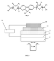
- FIG. 1 is the general formula of the quinoid silafluorene organic semiconductor material according to the embodiments of the present invention
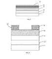
- FIG. 2 is a structural schematic view of a organic solar cell device comprising the quinoid silafluorene organic semiconductor material prepared in Example 1 as an active layer;
- FIG. 3 is a structural schematic view of an organic electroluminescent device comprising the quinoid silafluorene organic semiconductor material prepared in Example 1 as a luminescent layer;
- FIG. 4 is a structural schematic view of an organic field effect transistor device comprising the quinoid silafluorene organic semiconductor material prepared in Example 1 as an organic semiconductor layer.
- a quinoid silafluorene organic semiconductor material according to the embodiments of the present invention is shown, the general formula (I) thereof is as follows:
- R 1 , R 2 , R 5 and R 6 are independently selected from the group consisting of -H and C 1 -C 20 alkyl, R 3 and R 4 are independently C 1 -C 20 alkyl, m and n are independently integers of 0-10.
- R 1 , R 2 , R 5 and R 6 are preferably -C 6 H 13 or -C 20 H 41 alkyl, R 3 and R 4 are preferably -CH 3 , -C 6 H 13 or -C 20 H 41 alkyl.
- the fluorenyl increases the density of backbone electron atmosphere of the semiconductor material effectively, narrows the band gap of the semiconductor material, and increases the potential application value thereof in the organic semiconductor material.
- the embodiments of the present invention provide the method for manufacturing the quinoid silafluorene organic semiconductor material, comprising:
- R 1 , R 2 , R 5 and R 6 are independently selected from the group consisting of H and C 1 -C 20 alkyl, R 3 and R 4 are independently C 1 -C 20 alkyl, m and n are independently integers of 0-10;
- general formula ( ⁇ ') is a special case of general formula (I) when both m and n are 0.
- the compounds B and C in the above step (1) are commercially available, or may be prepared by the exiting synthesis method, and the method for preparing compound A comprises following steps:
- the molar ratio of 4,4 '- dibromo - 2,2' - diiodo-biphenyl, alkyl lithium derivative, dialkyl dichlorosilane is preferably 1.0: 2.0-4.0: 2.0-4.0; the said organic solvent is preferably one or more selected from the group consisting of tetrahydrofuran, diethyl ether, dichloromethane, chloroform, ethyl acetate; the temperature of this step is preferably -100 to -25 ⁇ , the duration thereof is preferably 24-48 hours.
- the molar ratio of 2,7 - dibromo -9,9 - dialkyl silafluorene compound, alkyl lithium derivative, 2 - isopropoxy-4,4,5,5 - tetramethyl-1,3,2 - dioxaborolane is preferably 1.0: 2.0-4.0: 2.0-4.0; the said organic solvent is preferably one or more selected from the group consisting of tetrahydrofuran, diethyl ether, dichloromethane, chloroform, ethyl acetate; the temperature of this step is preferably -100 to -25 ⁇ , the duration thereof is preferably 24-48 hours.
- the above steps a) and/or b) may be carried out under oxygen or oxygen-free environment.
- the oxygen-free environment is preferred, and the oxygen-free environment may be achieved by vacuum evacuation or being filled with in inert gas, and be filled with inert gas is preferred, the inert gas is commonly used in prior art, e.g. nitrogen, argon, the nitrogen is preferred.
- the reaction under oxygen-free environment may have an increased yield in every reaction step, as oxygen is a very active ingredient, which may react with the reactants, interfering with the progress of the reaction, thus reducing the product yield.
- the alkyl lithium derivative in steps a) and/or b) is preferably one or more selected from the group consisting of N-butyl lithium, tert-butyl lithium, methyl lithium and phenyl lithium.
- the alkali in the alkaline environment of the Suzuki coupling reaction step of the step (2) is one or more selected from the group consisting of NaOH, Na 2 CO 3 , NaHCO 3 and tetraethyl ammonium hydroxide;
- the said catalyst is preferably one or more selected from the group consisting of Pd(PPh 3 ) 4 , Pd 2 (dba) 3 /P( o -Tol) 3 , Pd(PPh 3 ) 2 Cl 2 , and the amount thereof is 0.05% -20% molar percent of that of the compound A;
- the said organic solvent is preferably one or more selected from the group consisting of ethylene glycol dimethyl ether, tetrahydrofuran, diethyl ether, dichloromethane, chloroform and ethyl acetate.
- the temperature of the Suzuki coupling reaction is preferably 75 -120°C, the duration thereof is preferably 12 - 72 hours.
- a catalyst is necessary for the Suzuki coupling reaction, since the catalyst has the following features: first, it can effectively improve the yield of Compound E of the present invention; second, it can improve the reaction rate of the Suzuki coupling reaction, and shorten the reaction time, increase production efficiency; third, as the catalyst is necessary for the Suzuki coupling reaction, which may react with one reactant in the reaction to obtain an intermediate product, thereby the Suzuki coupling reaction can be carried out.
- the above Suzuki coupling reaction can be carried out in an oxygen or oxygen-free environment.
- the oxygen-free environment can be achieved by vacuum evacuation or being filled with an inert gas, preferably by being filled with an inert gas, the inert gas is commonly used in the art, such as nitrogen, argon, etc., and nitrogen is preferred.
- the yield of the compound E may be improved, as oxygen is a very active ingredient, which can react with the reactants, interfering with the progress of the reaction, thus reducing the product yield.
- the molar ratio of compound E and N-bromo-succinimide in the above bromination reaction step of step (3) is preferably 1.0: 2.0-2.5;
- the organic solvent is preferably one or more selected from the group consisting of N, N-dimethyl formamide (DMF), tetrahydrofuran, diethyl ether, dichloromethane, chloroform, ethyl acetate and acetic acid.
- the temperature of the bromination reaction is preferably -5-30 °C, the duration thereof is preferably 12 -48 hours.
- the molar ratio of the dibromo compound of compound E and malononitrile in the above condensation reaction of the step (4) is preferably 1.0: 2.0-10;
- the organic solvent is preferably one or more selected from the group consisting of ethylene glycol dimethyl ether, tetrahydrofuran, diethyl ether, dichloromethane, chloroform and ethyl acetate.
- the said condensing agent is preferably one or more selected from the group consisting of NaH and sodium alkoxide, and more preferably the condensing agent is NaH, wherein the sodium alkoxide is preferably but not limited to sodium methoxide, sodium tert-butoxide.
- the temperature of the condensation reaction is preferably 75- 120 °C, the duration thereof is preferably 12- 72 hours; the said catalyst is preferably one or more selected from the group consisting of Pd(PPh 3 ) 4 , Pd 2 (dba)3, Pd(PPh 3 ) 2 Cl 2 , the amount thereof is 0.05% - 20% molar percentage of that of the dibromo compound of compound E.
- the reactants may be added in a certain ratio, and no other special equipment and environmental are required, the method has a simple process, high yield, mild reaction condition, it is easy to operate and control, suitable for industrial production.
- the quinoid silafluorene organic semiconductor material may be used in the fields of organic photoelectric materials, polymer solar cells, organic electroluminescent elements, organic field effect transistors, organic optical storage elements, organic nonlinear materials and/or organic laser elements.
- the solar cell device comprises a glass substrate 11, a transparent anode 12, a middle auxiliary layer 13, an active layer 14, a cathode 15 in a stacked structure, wherein the middle auxiliary layer 13 is made from poly(3,4-ethylenedioxythiophene): polystyrene-sulfonic acid composite(abbreviated as PEDOT:PSS), the active layer 14 includes an electron donor material and an electron acceptor material, and the electron donor material is made from the quinoid silafluorene organic semiconductor material made in Example 1, the electron acceptor material may be [6,6]phenyl- C 61 - butyric acid methyl ester(abbreviated as PCBM).
- PCBM quinoid silafluorene organic semiconductor material
- the transparent anode 12 may be made from Indium Tin Oxide(abbreviated as ITO), preferably from the Indium Tin Oxide with the sheet resistance of 10-20 ⁇ / ⁇ .
- the cathode 15 may be an aluminum electrode or a double-metal-layer electrode, for example, Ca/Al, or Ba/Al and the like.
- the glass substrate 11 may be used as the bottom layer.
- an ITO glass is selected, then it is ultrasonic washed, and treated with Oxygen-Plasma, then the middle auxiliary layer 13 is coated on the ITO glass, and the quinoid silafluorene organic semiconductor material made in Example 1 and the electron acceptor material are blended before coated on the middle auxiliary layer 13, thus formed the active layer 14 thereon, then the cathode 15 is deposited on the active layer 14 by vacuum evaporation to obtain the solar cell device.
- the thicknesses of the transparent anode 12, middle auxiliary layer 13, active layer 14, double-metal-layer Ca -Al layers are 170, 40, 150, 70 nm respectively.
- the light passes through the glass substrate 11 and the ITO electrode 12, and the quinoid silafluorene organic semiconductor material made in Example 1 in the active layer 14 absorbs light energy and generates exactions, then these exactions migrate to the interface between the electron donor / acceptor materials, and the electron is transferred to the electron acceptor material, such as PCBM, so as to achieve the separation of the charge, and to produce free carriers, i.e. free electrons and holes.
- the electron acceptor material such as PCBM
- the quinoid silafluorene organic semiconductor material prepared in Example 1 may utilize the light energy more sufficiently due to its very wide spectral response range, and have higher photoelectric conversion efficiency, thus the power production capacity of the solar cell device is increased. Furthermore this organic material may reduce the weight of the solar cell device containing the same, and can be produced by spin coating technology, and may be prepared in large scale.
- an organic electroluminescent apparatus containing the quinoid silafluorene organic semiconductor material made in Example 1 includes a glass substrate 21, a transparent anode 22, a luminescent layer 23, a buffer layer 24 and a cathode 25 in a stacked structure.
- the transparent anode 22 may be made from Indium Tin Oxide(abbreviated as ITO), preferably from the Indium Tin Oxide with the sheet resistance of 10-20 ⁇ / ⁇ .
- the luminescent layer 23 includes the quinoid silafluorene organic semiconductor material prepared in the Example 1.
- the buffer layer 24 may be made from, but not limited to, LiF and the like.
- the cathode 25 may be Al and the like, but not limited thereto.
- the organic electroluminescence apparatus may be represented by the structure: ITO/the quinoid silafluorene organic semiconductor material made in Example 1/LiF/Al.
- Each of the layers may be made by the exiting method, and the quinoid silafluorene organic semiconductor material made in Example 1 may be formed on the ITO by spin coating.
- the LiF buffer layer may be vacuum evaporated on the luminescent layer, and the metal Al may be evaporated on the buffer layer and used as a cathode of the apparatus.
- the organic field effect transistor contains a substrate 31, an insulating layer 32, a modifying layer 33, an organic semi-conductor layer 34 and a source electrode 35 and a drain electrode 36 disposed on the organic semi-conductor layer 34 in a stacked structure.
- the substrate 31 may be, but not limited to heavy doped silicon(Si)
- the insulating layer 32 may be, but not limited to, SiO 2 with the thickness of micro-nanometer (e.g., 450 nm).
- the organic semi-conductor layer 34 is made of the quinoid silafluorene organic semiconductor material prepared in Example 1. Both of the source electrode 35 and the drain electrode 36 may be made from aurum, but not limited thereto.
- the modifying layer 33 may be, but not limited to, octadecyl trichlorosilane(OTS).
- OTS octadecyl trichlorosilane
- Each of the substrate 31, the insulating layer 32, the modifying layer 33 and the source electrode 35 and the drain electrode 36 may be made by the exiting method.
- the organic semi-conductor layer 34 may be made by spin coating the quinoid silafluorene organic semiconductor material prepared in the Example 1 on the insulating layer 32 modified by modifying layer 33 under a vacuum degree of nearly 10 -4 Pa.
Landscapes
- Chemical & Material Sciences (AREA)
- Organic Chemistry (AREA)
- Engineering & Computer Science (AREA)
- Materials Engineering (AREA)
- Health & Medical Sciences (AREA)
- Chemical Kinetics & Catalysis (AREA)
- Medicinal Chemistry (AREA)
- Polymers & Plastics (AREA)
- Physics & Mathematics (AREA)
- Spectroscopy & Molecular Physics (AREA)
- Photovoltaic Devices (AREA)
- Low-Molecular Organic Synthesis Reactions Using Catalysts (AREA)
Abstract
Description
- The present invention relates to the technical field of synthesis of organic compound, particularly, to a quinoid silafluorene organic semiconductor material, preparation method and use thereof.
- The economy all over the world today is built on the basis of fossil fuel, such as coal, oil and natural gas. However, all of these non-reproducible fossil energies are continuously exhausted. Since the beginning of the 21st century, the global energy problems and the consequent problems of environmental pollution and climate warming are becoming more and more prominent and gradually intensified. Because of the outstanding advantages of wide and broad distribution, large scale resources, pollution-free, clean, safe, and easy to obtain, the solar energy is considered to be one of the most promising renewable energy. The solar cell converts the solar energy to electric energy directly, thus it is a practicable method for utilizing the solar energy. However, currently commercial solar cells are all limited to the silicon-based inorganic solar cell, but the cost is so high that people cannot accept it, thus the scope of their use is significantly limited. For a long time, to reduce the cost of the solar cell and expand the range of application, people have been looking for new type of solar cell materials.
- The organic solar cell is a new type of solar cell. Compared to the disadvantages of limited source, expensive price, toxic, complicated manufacturing process and high cost of the inorganic semiconductor material, the organic solar cell has the incomparable advantages that the inorganic solar cell doesn't have, such as wide sources of raw materials, a variety of structures and good adjustability, low cost, safety and environmental protection, simple manufacturing process, light weight, possibly to produce in a large flexibly area, and the like, it can be widely used in construction, lighting and power generation and other areas, thus it has an important development and application prospects. Therefore, many domestic and foreign research institutes and enterprises are paying considerable attention and investment to the field of organic solar cell. However, until now, the photoelectric conversion efficiency of the organic solar cell is much lower than that of inorganic solar cell. Therefore, the development of new organic photovoltaic materials has much importance for improving the efficiency of organic solar cells and other semiconductor devices.
- To overcome the above shortcomes in prior art, the present invention provides a quinoid silafluorene organic semiconductor material with high solubility and stability, and low energy band gap, so as to broaden the absorption range of solar spectrum of the solar cell, improve the photoelectric conversion efficiency thereof.
- Another object of the present invention is to provide a method for manufacturing the quinoid silafluorene organic semiconductor material with simple process, high yield, and it is easy to operate and control.
- A further object of the present invention is to provide the use of the aforementioned quinoid silafluorene organic semiconductor material in the fields of organic photoelectric materials, polymer solar cells, organic electroluminescent elements, organic field effect transistors, organic optical storage elements, organic nonlinear materials and/or organic laser elements.
- The above-mentioned technical problems can be solved through the following technical solutions:
- A quinoid silafluorene organic semiconductor material, the general formula (I) thereof is as follows :

- wherein, R1, R2, R5 and R6 are independently selected from the group consisting of H and C1-C20 alkyl, R3 and R4 are independently C1-C20 alkyl, m and n are independently integers of 0-10.
- And, a method for manufacturing a quinoid silafluorene organic semiconductor material, comprising:
- compounds A, B, C and D with following general formulae are provided separately:


- wherein R1, R2, R5 and R6 are independently selected from the group consisting of H and C1-C20 alkyl, R3 and R4 are independently C1-C20 alkyl, m and n are independently integers of 0-10;
- in an alkaline environment and with the present of a catalyst and an organic solvent, the Suzuki coupling reaction of compounds A, B and C is carried out to give the compound E of following formula:

- with the present of an organic solvent, the bromination reaction of compound E and N-bromo-succinimide is carried out to give a dibromo compound of compound E;
- with the present of a catalyst, a condensing agent and an organic solvent, the condensation reaction of the dibromo compound of compound E and malononitrile is carried out to give the quinoid silafluorene organic semiconductor material of general formula (I), wherein, m and n are independently integers of 1-10;
- alternatively, with the present of a catalyst, a condensing agent and an organic solvent, the condensation reaction of compound D and malononitrile is carried out to give the quinoid silafluorene organic semiconductor material of general formula (I), wherein m =n=0,

- Furthermore, the use of the quinoid silafluorene organic semiconductor material of the present invention in the fields of organic photoelectric materials, polymer solar cells, organic electroluminescent elements, organic field effect transistors, organic optical storage elements, organic nonlinear materials and/or organic laser elements.
- The quinoid silafluorene organic semiconductor material and the preparation method thereof according to the present invention have at least following advantages compared to the prior art:
- 1. it is easy to introduce an alkyl into the quinoid silafluorene organic semiconductor material, which increases the solubility of the material;
- 2. the dicyanovinyl ( = C(CN)2) contained therein is a strong electron withdrawing group, when introduced into a quinoid structure with strong conjugacy, it not only increases the stability of the material, but also facilitates lowering the energy band gap of the material, thus the absorption range of solar spectrum is broadened, and the photoelectric conversion efficiency is improved;
- 3. the method for manufacturing the quinoid silafluorene organic semiconductor material is simply, has the advantages of high yield, mild condition for reaction, easy to operate and control, and it is suitable for industrial production.
-
FIG. 1 is the general formula of the quinoid silafluorene organic semiconductor material according to the embodiments of the present invention; -
FIG. 2 is a structural schematic view of a organic solar cell device comprising the quinoid silafluorene organic semiconductor material prepared in Example 1 as an active layer; -
FIG. 3 is a structural schematic view of an organic electroluminescent device comprising the quinoid silafluorene organic semiconductor material prepared in Example 1 as a luminescent layer; -
FIG. 4 is a structural schematic view of an organic field effect transistor device comprising the quinoid silafluorene organic semiconductor material prepared in Example 1 as an organic semiconductor layer. - Objects, advantages and embodiments of the present invention will be explained below in detail with reference to the accompanying drawings and embodiments. However, it should be appreciated that the following description of the embodiment is merely exemplary in nature and is not intended to limit this invention.
- Referring to
FIG. 1 , a quinoid silafluorene organic semiconductor material according to the embodiments of the present invention is shown, the general formula (I) thereof is as follows:
- wherein, R1, R2, R5 and R6 are independently selected from the group consisting of -H and C1-C20 alkyl, R3 and R4 are independently C1-C20 alkyl, m and n are independently integers of 0-10. R1, R2, R5 and R6 are preferably -C6H13 or -C20H41 alkyl, R3 and R4 are preferably -CH3, -C6H13 or -C20H41 alkyl.
- In the above quinoid silafluorene organic semiconductor material according to the embodiments of the present invention, it is easy to introduce an alkyl, and the introduction of alkyl improves the original rigidity of the molecular, thereby in the same solvent, compared to the molecular without introduction of alkyl, the solubility of the quinoid silafluorene organic semiconductor material according to the embodiments of the present invention, is increased effectively, meanwhile the quinoid silafluorene organic semiconductor material contains dicyanovinyl ( = C(CN)2), which is a strong electron withdrawing group, when introduced into a quinoid structure with strong conjugacy, it not only increases the stability of the material, but also facilitates lowering the energy band gap of the material, thus the absorption range of solar spectrum is broadened, and the photoelectric conversion efficiency is improved. And the fluorenyl increases the density of backbone electron atmosphere of the semiconductor material effectively, narrows the band gap of the semiconductor material, and increases the potential application value thereof in the organic semiconductor material.
- Also, the embodiments of the present invention provide the method for manufacturing the quinoid silafluorene organic semiconductor material, comprising:
- (1) compounds A, B, C and D with following general formulae are provided separately:


- wherein R1, R2, R5 and R6 are independently selected from the group consisting of H and C1-C20 alkyl, R3 and R4 are independently C1-C20 alkyl, m and n are independently integers of 0-10;
- (2) in an alkaline environment and with the present of a catalyst and an organic solvent, the Suzuki coupling reaction of compounds A, B and C is carried out to give the compound E, the chemical equation thereof is as follows:

- (3) with the present of an organic solvent, the bromination reaction of compound E and N-bromo-succinimide is carried out to give a dibromo compound F of compound E, the chemical equation thereof is as follows:

- (4) with the present of a catalyst, a condensing agent and an organic solvent, the condensation reaction of the dibromo compound F of compound E and malononitrile is carried out to give the quinoid silafluorene organic semiconductor material of following general formula (I), wherein, m and n are independently integers of 1-10, the chemical equation thereof is as follows:

- Alternatively, with the present of a catalyst, a condensing agent and an organic solvent, the condensation reaction of compound D and malononitrile is carried out to give the quinoid silafluorene organic semiconductor material of general formula (I'), the chemical equation thereof is as follows:

- wherein general formula (□') is a special case of general formula (I) when both m and n are 0.
- The compounds B and C in the above step (1) are commercially available, or may be prepared by the exiting synthesis method, and the method for preparing compound A comprises following steps:
- a) with the present of an organic solvent, the reaction of 4,4 '- dibromo - 2,2' - diiodo-biphenyl, alkyl lithium derivative and dialkyl dichlorosilane is carried out to give a compound of 2,7 - dibromo-9 ,9 - dialkylsilafluorene, the chemical equation of this step is as follows:

- b) with the present of an organic solvent, the reaction of 2,7 - dibromo -9,9 - dialkyl silafluorene compound, alkyl lithium derivative, 2 - isopropoxy-4,4,5,5 - tetramethyl-1,3,2 - dioxaborolane is carried out to give the compound A, the chemical equation of this step is as follows:

- In the above step a), the molar ratio of 4,4 '- dibromo - 2,2' - diiodo-biphenyl, alkyl lithium derivative, dialkyl dichlorosilane is preferably 1.0: 2.0-4.0: 2.0-4.0; the said organic solvent is preferably one or more selected from the group consisting of tetrahydrofuran, diethyl ether, dichloromethane, chloroform, ethyl acetate; the temperature of this step is preferably -100 to -25 □, the duration thereof is preferably 24-48 hours.
- In the above step b), the molar ratio of 2,7 - dibromo -9,9 - dialkyl silafluorene compound, alkyl lithium derivative, 2 - isopropoxy-4,4,5,5 - tetramethyl-1,3,2 - dioxaborolane is preferably 1.0: 2.0-4.0: 2.0-4.0; the said organic solvent is preferably one or more selected from the group consisting of tetrahydrofuran, diethyl ether, dichloromethane, chloroform, ethyl acetate; the temperature of this step is preferably -100 to -25 □, the duration thereof is preferably 24-48 hours.
- The above steps a) and/or b) may be carried out under oxygen or oxygen-free environment. The oxygen-free environment is preferred, and the oxygen-free environment may be achieved by vacuum evacuation or being filled with in inert gas, and be filled with inert gas is preferred, the inert gas is commonly used in prior art, e.g. nitrogen, argon, the nitrogen is preferred. This is because the reaction under oxygen-free environment may have an increased yield in every reaction step, as oxygen is a very active ingredient, which may react with the reactants, interfering with the progress of the reaction, thus reducing the product yield. The alkyl lithium derivative in steps a) and/or b) is preferably one or more selected from the group consisting of N-butyl lithium, tert-butyl lithium, methyl lithium and phenyl lithium.
- In the general formula of compound E obtained by the Suzuki coupling reaction in the above step (2), when m = n = 0, in step (1) only compounds D and malononitrile take part in the condensation reaction, and the quinoid silafluorene organic semiconductor material of general formula (I) with m = n = 0 is obtained, wherein the compound D is commercially available; when m = 0 and 0 <n ≤ 10, only compounds A and C are selected for the coupling reaction of step (2) to obtain the quinoid silafluorene organic semiconductor material of general formula (I) with m = 0 and 0 <n ≤ 10; when n = 0, 0 < m≤10, only compounds A and B are selected for the coupling reaction of step (2) to obtain the quinoid silafluorene organic semiconductor material of general formula (I) with n = 0 and 0 < m≤10; when 0 < m≤10 and 0 < n≤10, compounds A, B and C all are selected for the coupling reaction of step (2) to obtain the quinoid silafluorene organic semiconductor material of general formula (I) with 0 < m≤10 and 0 < n≤10, when 0 < m≤10 and 0 < n≤10, the molar ratio of compounds A, B and C is preferably 1.0: 1.0-1.5: 1.0-1.5, wherein, the molar ratio of compound B and C is preferably 1:1.
- The alkali in the alkaline environment of the Suzuki coupling reaction step of the step (2) is one or more selected from the group consisting of NaOH, Na2CO3, NaHCO3 and tetraethyl ammonium hydroxide; the said catalyst is preferably one or more selected from the group consisting of Pd(PPh3)4, Pd2(dba)3/P(o-Tol)3, Pd(PPh3)2Cl2, and the amount thereof is 0.05% -20% molar percent of that of the compound A; the said organic solvent is preferably one or more selected from the group consisting of ethylene glycol dimethyl ether, tetrahydrofuran, diethyl ether, dichloromethane, chloroform and ethyl acetate. The temperature of the Suzuki coupling reaction is preferably 75 -120°C, the duration thereof is preferably 12 - 72 hours. A catalyst is necessary for the Suzuki coupling reaction, since the catalyst has the following features: first, it can effectively improve the yield of Compound E of the present invention; second, it can improve the reaction rate of the Suzuki coupling reaction, and shorten the reaction time, increase production efficiency; third, as the catalyst is necessary for the Suzuki coupling reaction, which may react with one reactant in the reaction to obtain an intermediate product, thereby the Suzuki coupling reaction can be carried out.
- The above Suzuki coupling reaction can be carried out in an oxygen or oxygen-free environment. Preferably it is carried out in an oxygen-free environment, and the oxygen-free environment can be achieved by vacuum evacuation or being filled with an inert gas, preferably by being filled with an inert gas, the inert gas is commonly used in the art, such as nitrogen, argon, etc., and nitrogen is preferred. This is because in an oxygen-free environment, the yield of the compound E may be improved, as oxygen is a very active ingredient, which can react with the reactants, interfering with the progress of the reaction, thus reducing the product yield.
- The molar ratio of compound E and N-bromo-succinimide in the above bromination reaction step of step (3) is preferably 1.0: 2.0-2.5; the organic solvent is preferably one or more selected from the group consisting of N, N-dimethyl formamide (DMF), tetrahydrofuran, diethyl ether, dichloromethane, chloroform, ethyl acetate and acetic acid. The temperature of the bromination reaction is preferably -5-30 °C, the duration thereof is preferably 12 -48 hours.
- The molar ratio of the dibromo compound of compound E and malononitrile in the above condensation reaction of the step (4) is preferably 1.0: 2.0-10; the organic solvent is preferably one or more selected from the group consisting of ethylene glycol dimethyl ether, tetrahydrofuran, diethyl ether, dichloromethane, chloroform and ethyl acetate. The said condensing agent is preferably one or more selected from the group consisting of NaH and sodium alkoxide, and more preferably the condensing agent is NaH, wherein the sodium alkoxide is preferably but not limited to sodium methoxide, sodium tert-butoxide. The temperature of the condensation reaction is preferably 75- 120 °C, the duration thereof is preferably 12- 72 hours; the said catalyst is preferably one or more selected from the group consisting of Pd(PPh3)4, Pd2(dba)3, Pd(PPh3)2Cl2, the amount thereof is 0.05% - 20% molar percentage of that of the dibromo compound of compound E.
- In this method for manufacturing a quinoid silafluorene organic semiconductor material, the reactants may be added in a certain ratio, and no other special equipment and environmental are required, the method has a simple process, high yield, mild reaction condition, it is easy to operate and control, suitable for industrial production.
- Because of the above advantages of the quinoid silafluorene organic semiconductor material, the quinoid silafluorene organic semiconductor material may be used in the fields of organic photoelectric materials, polymer solar cells, organic electroluminescent elements, organic field effect transistors, organic optical storage elements, organic nonlinear materials and/or organic laser elements.
- The present invention will be explained in detail referring to Examples.
- Example 1
- Preparation of the quinoid silafluorene organic semiconductor material with following structural formula I1:

- 1) Preparation of 2, 7 - dibromo-9, 9 - dimethyl silafluorene, the structural formula and preparation method there of are as follows:

- under the protection of nitrogen, 5.64 g of 4, 4'-dibromo-2, 2'-diiodo biphenyl was dissolved in 40 mL of THF, cooled to -25 °C, to the solution was added dropwise 20.00 mL of n-butyl lithium solution (n-butyl lithium/n-hexane in 1.0 mol / L). After 2 hours of reaction, 1.29 g of dimethyl dichlorosilane was added, and the reaction was continued for another 24 hours. After the completion of the reaction, a deionized water was added and the resulting mixture was extracted with diethyl ether, then dried over anhydrous magnesium sulfate, rotary evaporated, and column chromatographed to give the product. MALDI-TOF-MS (m / z): 368.1 (M+);
- 2) Preparation of the quinoid silafluorene organic semiconductor material with following structural formula I1, the method for preparation is as follows:
- in ice bath, 3.14 g ofmalononitrile was added to the suspension of 2.45 g of sodium hydride (60% in oil solution) in 50 mL of ethylene glycol dimethyl ether, then the mixture was warmed to room temperature, stirred for 20 minutes and 3.68 g of 2, 7 - dibromo-9, 9 - dimethyl silafluorene and 0.54 g of PdCl2(PPh3)2 were added.
The mixture was heated to 120 °C for 12 hours, cooled to 0 °C, and saturated Br2/H2O solution was added. A water was added, and the resulting mixture was vacuum filtered, washed with water, dried, and column chromatographed to give the product. MALDI-TOF-MS (m / z): 336.4 (M +). - Example 2
- Preparation of the quinoid silafluorene organic semiconductor material with following structural formula I2:

- 1) Preparation of 2, 7 - dibromo-9, 9 - dihexyl silafluorene, the structural formula and preparation method are as follows:

- Under the protection of argon, 6.00 g of 4, 4'-dibromo-2, 2'-diiodo biphenyl was dissolved in 100 mL of THF, cooled to -100 °C, then to the solution 42.55 mL of methyl lithium solution (methyl lithium/n-hexane in 1.0 M) was added dropwise. After 12 hours of reaction, 5.70 g dihexyl dichlorosilane was added, and the reaction was continued for another 48 hours, the reaction was completed, then a water was added, and the mixture was extracted with diethyl ether, dried over anhydrous magnesium sulfate, rotary evaporated, and column chromatographed to give the product, MALDI-TOF-MS (m/z): 508.4 (M +);
- 2) Preparation of 2,7 - bis (4, 4, 5, 5 - tetramethyl-1, 3, 2 -dioxaborolan) - 9, 9- dihexyl silafluorene, the structural formula and preparation process thereof are as follows:
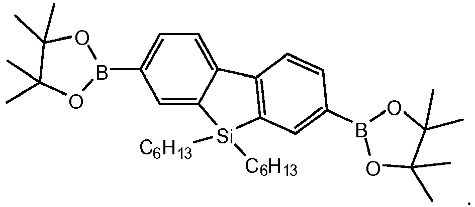
- At -25 °C, under nitrogen, 10.00 mL (2.00 M) of n-butyl lithium solution was added to a reaction flask containing 5.08 g of 2, 7 - dibromo-9, 9 - dihexyl silafluorene and 50 mL of tetrahydrofuran, stirred for 2 hours, then 4.17 mL of 2 - isopropoxy-4, 4, 5, 5 - tetramethyl-1, 3, 2 - dioxaborolane was added dropwise slowly, and stirred for another 24 hours, the reaction was completed, then the fluid mixture was poured into water and the solution was extracted with diethyl ether, dried over anhydrous magnesium sulfate, rotary evaporated, and column chromatographed to give a solid product, MALDI-TOF-MS (m / z): 602.5 (M +);
- 3) Preparation of 3, 7 - bis (thiophen-2 - yl) - 9,9- dihexyl silafluorene, the structural formula and preparation process thereof are as follows:

- Under the protection of nitrogen, to a reaction flask containing 3.01 g of 2, 7 - bis (4, 4, 5, 5 - tetramethyl-1, 3, 2 - dioxaborolan) - 9, 9 - dihexyl silafluorene, 1.63 g of 2 - bromo-thiophene and 0.34 g of Pd(PPh3)4, 40 mL of aqueous NaHCO3 solution (1 M) and ethylene glycol dimethyl ether (60 mL) were added, after purged with nitrogen for 1 hour, the solution was heated at 120 °C for 12 hours, the reaction was completed, then the mixture was filtered and dried in vacuo, column chromatographed to give a solid product, MALDI-TOF-MS (m / z): 514.9 (M +);
- 4) Preparation of 3, 7 - bis (5 - bromo-thiophen-2 - yl) - 9,9 - dihexyl silafluorene, the structural formula and preparation process thereof are as follows:

- At -5 °C, 0.71 g of NBS was added in batch to a reaction flask containing 1.30 g of 5, 5 - dihexyl-3, 7 - bis (thiophen-2 - yl)-4H-bis silafluorene and 20 mL of DMF, stirred for 48 hours. After the completion of the reaction, the fluid mixture was poured into ice-water for quenching, then it was extracted with chloroform, dried over anhydrous magnesium sulfate, and rotary evaporated, and column chromatographed to give the product, MALDI-TOF- MS (m / z): 672.7 (M +),
- Preparation of the quinoid silafluorene organic semiconductor material of structural formula I2, the method for preparation is as follows:
- In ice bath, 1.57 g of malononitrile was added to the suspension of 0.19 g of sodium hydride (sodium hydride in oil in 60wt%) in 25 mL of ethylene glycol dimethyl ether, then warmed to room temperature, stirred for 30 minutes and 0.67 g of 5, 5 - di-hexyl-3, 7 - bis (5 - bromo-thiophen-2 - yl)-4H-bis silafluorene and 0.034 g of PdCl2(PPh3)2 were added. The mixture was heated at 75 °C for 72 hours, then cooled to 0°C, and saturated Br2/H2O solution was added. A water was added, and the mixture was vacuum filtered, washed with water, dried, and column chromatographed to give the product. MALDI-TOF-MS (m / z): 640.9 (M +).
- Example 3
- Preparation of the quinoid silafluorene organic semiconductor material of following structural formula I3:

- 1) preparation of 2, 7 - bis (4, 4, 5, 5 - tetramethyl -1, 3, 2-dioxaborolan) - 9, 9 - dihexyl silafluorene, the detailed preparation process thereof is the same as step 2) of Example 2, and its structural formula is as follows:

- 2) preparation of 3, 7 - bis (4 - hexyl thiophen -2 - yl) - 9, 9 - dihexyl silafluorene, and the structural formula and preparation process are as follows:

- Under the protection of nitrogen, to a reaction flask containing 3.01 g of 2, 7 - bis (4, 4, 5, 5 - tetraethyl-1, 3, 2 - dioxaborolan) - 9, 9 - dihexyl silafluorene, 2.68 g of 2- bromo-4 - hexyl thiophene and 0.15 g of Pd(PPh3)4, 30 mL of aqueous NaOH (1 M) solution and chloroform (50 mL) were added, purged with nitrogen for 1 hour, then heated at 75°C for 72 hours, the reaction was completed, the mixture was filtered and dried in vacuo, column chromatographed to give a solid product, MALDI-TOF-MS (m / z): 683.2 (M +);
- 3) preparation of 3, 7 - bis (5 - bromo-4-hexyl thiophen-2 - yl) - 9, 9 - dihexyl silafluorene, and the structural formula and preparation process thereof are as follows:

- At 0 □, 0.89 g of NBS was added in batch to a reaction flask containing 1.37 g of 5, 5 - di-hexyl-3, 7 - bis (4 - hexyl thiophen-2 - yl)-4H-bis silafluorene and 40 mL of DMF, stirred for 12 hours. After the completion of the reaction, the fluid mixture was poured into ice-water for quenching, then the solution was extracted with chloroform, dried over anhydrous magnesium sulfate, rotary evaporated, and column chromatographed to give the product, MALDI-TOF -MS (m / z): 841.0 (M +);
- 4) preparation of the quinoid silafluorene organic semiconductor material of structural formula I3, its preparation process is as follows:
- in ice bath, 0.25 g of malononitrile was added to the suspension of 0.21 g of sodium hydride (sodium hydride in an oil solution in 60wt%) in 30 mL of ethylene glycol dimethyl ether, warmed to room temperature and stirred for 30 minutes, then to the solution was added 0.84 g of 5, 5 - di-hexyl-3, 7 - bis (5 - bromo-4-hexyl thiophen-2 - yl)-4H-bis silafluorene and 0.038 g of PdCl2(PPh3)2, and heated at 90 °C for 52 hours, then cooled to 0 °C, saturated Br2/H2O solution was added, a water was added, then the mixture was vacuum filtered, and washed with water, dried, and column chromatographed to give the product, MALDI-TOF-MS (m / z): 809.3 (M +).
- Example 4
- Preparation of the quinoid silafluorene organic semiconductor material of following structural formula I4:

- 1) Preparation of 2, 7 - dibromo-9, 9 - bis-eicosyl silafluorene, and its structural formula and preparation method are as follows:

- 6.00 g of 4, 4'-dibromo-2, 2'-diiodobiphenyl was dissolved in 100 mL of a mixed solvent of dichloromethane and ethyl acetate in the volume ratio of 1:1, then cooled to -75 °C, and 30.00 mL of phenyl lithium solution (phenyl lithium/ n-hexane in 1.0 M,) was added dropwise. Following 10 hours of reaction, 14.56 g of bis-eicosyl dichlorosilane was added, and the reaction was continued for another 34 hours, after the reaction was completed, a water was added and the mixture was extracted with diethyl ether, dried over anhydrous magnesium sulfate, rotary evaporated, and column chromatographed to give the product, MALDI-TOF-MS (m / z): 901.2 (M+),
- 2) Preparation of 2,7 - bis (4, 4, 5, 5 - tetramethyl-1, 3, 2 - dioxaborolan) - 9, 9 - bis-eicosyl silafluorene, and the structural formula and preparation process are as follows:

- At -78 °C, under a nitrogen atmosphere, 20.00 mL (1.00 M) of n-butyl lithium solution was added to a reaction flask containing 4.50 g of 2,7 - dibromo-9, 9 - bis-eicosyl silafluorene and 100 mL of diethyl ether and stirred for 12 hours, then 4.17 mL of 2 - isopropoxy-4, 4, 5, 5 - tetramethyl-1, 3, 2 - dioxaborolane was added dropwise slowly, and stirred for another 48 hours. After the reaction was completed, the fluid mixture was poured into water then the solution was extracted with diethyl ether, dried over anhydrous magnesium sulfate, rotary evaporated, and column chromatographed to give a solid product, MALDI-TOF-MS (m / z): 995.3 (M+),
- 3) Preparation of 3, 7 - bis (4 - eicosyl thiophen-2 - yl) - 9, 9 - bis-eicosyl silafluorene, the structural formula and preparation process thereof are as follows:

- Under the protection of nitrogen, to a reaction flask containing 3.00 g of 2, 7 - bis (4, 4, 5, 5 - tetramethyl-1, 3, 2 - dioxaborolan) -9,9 - bis-eicosyl silafluorene, 2.92 g of 2 - bromo-4 - eicosyl thiophene and 0.25 g of Pd2(dba)3/P(o-Tol)3, 30 mL of aqueous tetraethyl ammonium hydroxide solution (1 M) and ethylene glycol dimethyl ether (50 mL) were added, then purged with nitrogen for 1 hour, and heated at 90 □ for 28 hours. After the reaction was completed, the mixture was filtered and dried in vacuo, column chromatographed to give a solid product, MALDI-TOF-MS (m / z): 1468.7 (M+);
- 4) Preparation of 3, 7 - bis (5 - bromo-4 - eicosyl thiophen -2 - yl) - 9,9 - bis-eicosyl silafluorene, and the structural formula and preparation process are as follows:

- At 30 □, 0.73 g of NBS was added in batch to a reaction flask containing 2.94 g of 5,5 - bis-eicosyl-3, 7 - bis (4 - eicosyl-thiophen-2- yl)-4H- disilafluorene and 40 mL of DMF, stirred for 18 hours. After the reaction was completed, the fluid mixture was poured into ice-water for quenching, then the solution was extracted with chloroform, and dried over anhydrous magnesium sulfate, rotary evaporated, and column chromatographed to give the product, MALDI- TOF- MS (m / z): 1626.5 (M+);
- 5) Preparation of the quinoid silafluorene organic semiconductor material of structural formula I4, the preparation process is as follows:
- In ice bath, 0.88 g of malononitrile was added to the suspension of 0.20 g of sodium hydride (sodium hydride in an oil solution in 60wt%) in 40 mL of ethylene glycol dimethyl ether, then warmed to room temperature and stirred for 30 minutes, to the mixture 1.63 g of 5, 5 - bis-eicosyl-3, 7 - bis(5 - bromo-4 - eicosyl-thiophen-2 - yl)-4H-bis silafluorene and 0.055 g of PdCl2(PPh3)2 were added, heated at 100 °C for 25 hours, then cooled to 0 °C, and a saturated Br2/H2O solution was added, then a water was added, and the solution was vacuum filtered, washed with water, dried, and column chromatographed to give the product, MALDI-TOF-MS (m / z ): 1594.7 (M+);
- Example 5
- Preparation of the quinoid silafluorene organic semiconductor material of following structural formula I5:

- 1) Preparation of 2, 7 - bis (4, 4, 5, 5 - tetramethyl -1, 3, 2 - dioxaborolan) - 9, 9 - dihexyl silafluorene, the detailed preparation process is the same as step 2) of Example 2, and its structural formula is as follows:

- 2) preparation of 3, 7 - bis (2, 2'-bithiophen -5 - yl) - 9, 9 - dihexyl silafluorene, the structural formula and preparation process thereof are as follows:
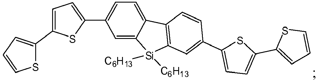
- under the protection of nitrogen, to a reaction flask containing 3.01 g of 2, 7 - bis (4, 4, 5, 5 - tetramethyl-1, 3, 2 - dioxaborolan) - 9, 9 - dihexyl silafluorene, 2.50 g of 5 - bromo-2, 2'-bithiophene and 0.21 g of Pd(PPh3)2Cl2, 30 mL aqueous NaHCO3 solution (1 M), and ethylene glycol dimethyl ether (50 mL) were added. Following purged with nitrogen for 1 hour, the mixture was heated at 100 °C for 25 hours, after the reaction was completed, the mixture was filtered and dried in vacuo, then column chromatographed to give a solid product, MALDI-TOF-MS (m / z): 679.1 (M+);
- 3) Preparation of 3, 7 - bis (5'-bromo-2, 2'-bithiophen -5 - yl) - 9, 9-dihexyl silafluorene, the structural formula and preparation process thereof are as follows:

- At 10 □, 0.71 g of NBS was added in batch to a reaction flask containing 1.36 g of 5, 5 - dihexyl-3, 7 - bis (2, 2'-bithiophen-5 - yl)-4H-bis- silafluorene and 20 mL of chloroform, stirred for 12 hours. After the reaction was completed, the fluid mixture was poured into ice-water for quenching, and the solution was extracted with chloroform, dried over anhydrous magnesium sulfate, rotary evaporated, and column chromatographed to give the product, MALDI-TOF- MS (m / z): 836.9 (M +);
- 4) Preparation of the quinoid silafluorene organic semiconductor material of structural formula I5, the preparation process is as follows:
- in ice bath, 0.33 g of malononitrile was added to the suspension of 0.20 g of sodium methoxide in 40 mL of ethylene glycol dimethyl ether, then the mixture was warmed to room temperature and stirred for 30 minutes, then 0.84 g of 5, 5 - dihexyl-3, 7 - bis(5'-bromo-2, 2'-bithiophen-5 - yl)-4H-bis-silafluorene and 0.043 g of PdCl2(PPh3)2 were added, and the resulting mixture was heated at 110 °C for 33 hours, then cooled to 0 □, a saturated Br2/H2O solution was added, then a water was added, and the mixture was vacuum filtered, washed with water, dried, and column chromatographed to give the product, MALDI-TOF-MS (m / z): 805.2 (M+).
- Example 6
- Preparation of the quinoid silafluorene organic semiconductor material of following structural formula I6:

- 1) Preparation of 2, 7 - bis (4, 4, 5, 5 - tetramethyl -1, 3, 2 - dioxaborolan) - 9, 9 - bis-eicosyl silafluorene, the detailed preparation process is the same as step 2) of Example 2, and its structural formula is as follows:

- 2) 3, 7 - bis (4, 4'-bis-eicosyl-2, 2'-bithiophen-5 - yl) - 9, 9 - bis-eicosyl silafluorene, the structure formula and preparation process thereof are as follows:

- To a reaction flask containing 9.95 g of 2, 7 - bis (4, 4, 5, 5 - tetramethyl-1, 3, 2 - dioxaborolan) - 9, 9 - bis-eicosyl silafluorene, 16.20 g of 5 - bromo-4, 4'-bis-eicosyl-2, 2'- bithiophene and 0.55 g of Pd(PPh3)4, 60 mL of aqueous NaHCO3 solution (1 M) and a mixed solvent (100 mL) of diethyl ether and dichloromethane in a volume ratio of 1:1 were added, then the mixture was heated at 85 °C for 32 hours. After the completion of the reaction, the resulting mixture was filtered and dried in vacuo, and column chromatographed to give a solid product, MALDI-TOF-MS (m / z): 2194.0 (M+);
- 3) 3,7 - bis(5'-bromo -4, 4'-bis-eicosyl-2, 2'-bithiophen -5 - yl) - 9, 9 - bis-eicosyl silafluorene, the structural formula and preparation process thereof are as follows:

- At 25 °C, 0.77 g of NBS was added in batch to a reaction flask containing 2.19 g of 5, 5 - bis-eicosyl-3,7- bis(4, 4'-bis-eicosyl-2, 2'-bithiophen-5-yl) -4H- bis-silafluorene and 40 mL of mixed solvent of tetrahydrofuran and ethyl acetate in a volume ratio of 1:3, then the mixture was stirred for 18 hours. After the completion of the reaction, the fluid mixture was poured into ice water for quenching, then the solution was extracted with chloroform, dried over anhydrous magnesium sulfate, rotary evaporated, and column chromatographed to give the product, MALDI-TOF-MS (m / z): 2351.8 (M+);
- 4) Preparation of the quinoid silafluorene organic semiconductor material of structural formula I6, the preparation process thereof is as follows:

- In ice bath, 0.49 g of malononitrile was added to the suspension of 0.10g of sodium tert-butoxide (sodium tert-butoxide in an oil solution in 60wt%) in 20 mL of ethylene glycol dimethyl ether, then the mixture was warmed to room temperature and stirred for 40 minutes, and 1.18 g of 5, 5 - bis-eicosyl-3,7- bis(5'-bromo- 4,4'-bis-eicosyl-2, 2'-bithiophen-5 - yl)-4H-bis-silafluorene and 0.033 g of PdCl2(PPh3)2 were added, and the mixture was heated at 95 °C for 42 hours, then cooled to 0 °C, and a saturated Br2/H2O solution was added, a water was added, then the resulting mixture was vacuum filtered, washed with water, dried, and column chromatographed to give the product, MALDI-TOF-MS (m / z): 2320.1(M+).
- Application Example 7
- Preparation of solar cell device containing the quinoid silafluorene organic semiconductor material made in Example 1 as an active layer:
- Referring to
FIG. 2 , the solar cell device comprises aglass substrate 11, atransparent anode 12, a middleauxiliary layer 13, anactive layer 14, acathode 15 in a stacked structure, wherein the middleauxiliary layer 13 is made from poly(3,4-ethylenedioxythiophene): polystyrene-sulfonic acid composite(abbreviated as PEDOT:PSS), theactive layer 14 includes an electron donor material and an electron acceptor material, and the electron donor material is made from the quinoid silafluorene organic semiconductor material made in Example 1, the electron acceptor material may be [6,6]phenyl- C61- butyric acid methyl ester(abbreviated as PCBM). Thetransparent anode 12 may be made from Indium Tin Oxide(abbreviated as ITO), preferably from the Indium Tin Oxide with the sheet resistance of 10-20 Ω/□. Thecathode 15 may be an aluminum electrode or a double-metal-layer electrode, for example, Ca/Al, or Ba/Al and the like. Theglass substrate 11 may be used as the bottom layer. In manufacturing, an ITO glass is selected, then it is ultrasonic washed, and treated with Oxygen-Plasma, then the middleauxiliary layer 13 is coated on the ITO glass, and the quinoid silafluorene organic semiconductor material made in Example 1 and the electron acceptor material are blended before coated on the middleauxiliary layer 13, thus formed theactive layer 14 thereon, then thecathode 15 is deposited on theactive layer 14 by vacuum evaporation to obtain the solar cell device. In a preferred embodiment, the thicknesses of thetransparent anode 12, middleauxiliary layer 13,active layer 14, double-metal-layer Ca -Al layers are 170, 40, 150, 70 nm respectively. - Referring to
FIG. 2 , under illumination ,the light passes through theglass substrate 11 and theITO electrode 12, and the quinoid silafluorene organic semiconductor material made in Example 1 in theactive layer 14 absorbs light energy and generates exactions, then these exactions migrate to the interface between the electron donor / acceptor materials, and the electron is transferred to the electron acceptor material, such as PCBM, so as to achieve the separation of the charge, and to produce free carriers, i.e. free electrons and holes. These free electrons are transferred along the electron acceptor material towards the metal cathode and collected by the cathode, meanwhile the free holes are transferred along the electron donor material towards the ITO anode and collected by the anode, to give photocurrent and photovoltage, and the photoelectric conversion is achieved. When there is anexternal load 16 connected to the device, the device will supply power to the external load. In this process, the quinoid silafluorene organic semiconductor material prepared in Example 1 may utilize the light energy more sufficiently due to its very wide spectral response range, and have higher photoelectric conversion efficiency, thus the power production capacity of the solar cell device is increased. Furthermore this organic material may reduce the weight of the solar cell device containing the same, and can be produced by spin coating technology, and may be prepared in large scale. - Application Example 8
- Preparation of organic electroluminescent apparatus containing the quinoid silafluorene organic semiconductor material made in Example 1:
- Referring to
FIG. 3 , an organic electroluminescent apparatus containing the quinoid silafluorene organic semiconductor material made in Example 1 is shown, the apparatus includes aglass substrate 21, atransparent anode 22, aluminescent layer 23, abuffer layer 24 and acathode 25 in a stacked structure. Thetransparent anode 22 may be made from Indium Tin Oxide(abbreviated as ITO), preferably from the Indium Tin Oxide with the sheet resistance of 10-20 Ω/□. Theluminescent layer 23 includes the quinoid silafluorene organic semiconductor material prepared in the Example 1. Thebuffer layer 24 may be made from, but not limited to, LiF and the like. Thecathode 25 may be Al and the like, but not limited thereto. Therefore, in a particular embodiment, the organic electroluminescence apparatus may be represented by the structure: ITO/the quinoid silafluorene organic semiconductor material made in Example 1/LiF/Al. Each of the layers may be made by the exiting method, and the quinoid silafluorene organic semiconductor material made in Example 1 may be formed on the ITO by spin coating. The LiF buffer layer may be vacuum evaporated on the luminescent layer, and the metal Al may be evaporated on the buffer layer and used as a cathode of the apparatus. - Application Example 9
- Preparation of organic field effect transistor containing the quinoid silafluorene organic semiconductor material made in Example 1:
- Referring to
FIG. 4 , the organic field effect transistor contains asubstrate 31, an insulatinglayer 32, a modifyinglayer 33, an organicsemi-conductor layer 34 and asource electrode 35 and adrain electrode 36 disposed on the organicsemi-conductor layer 34 in a stacked structure. Wherein thesubstrate 31 may be, but not limited to heavy doped silicon(Si), the insulatinglayer 32 may be, but not limited to, SiO2 with the thickness of micro-nanometer (e.g., 450 nm). The organicsemi-conductor layer 34 is made of the quinoid silafluorene organic semiconductor material prepared in Example 1. Both of thesource electrode 35 and thedrain electrode 36 may be made from aurum, but not limited thereto. The modifyinglayer 33 may be, but not limited to, octadecyl trichlorosilane(OTS). Each of thesubstrate 31, the insulatinglayer 32, the modifyinglayer 33 and thesource electrode 35 and thedrain electrode 36 may be made by the exiting method. The organicsemi-conductor layer 34 may be made by spin coating the quinoid silafluorene organic semiconductor material prepared in the Example 1 on the insulatinglayer 32 modified by modifyinglayer 33 under a vacuum degree of nearly 10-4Pa. - The embodiments above are merely the preferable embodiments of the present invention and not intended to limit the present invention. And all changes, equivalent substitution and improvements which come within the meaning and range of equivalency of the present invention are intended to be embraced therein.
Claims (10)
- A quinoid silafluorene organic semiconductor material, the general formula (I) thereof is:

- The quinoid silafluorene organic semiconductor material of claim 1, wherein the R1, R2, R5 and R6 are independently selected from the group consisting of -H, -C6H13 and -C20H41 alkyl, R3 and R4 are independently selected from the group consisting of -CH3, -C6H13 and -C20H41 alkyl.
- A method for manufacturing a quinoid silafluorene organic semiconductor material, comprising:compounds A, B, C and D with following general formulae are provided separately:
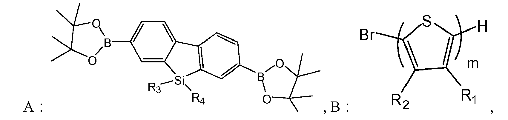
 in an alkaline environment and with the present of a catalyst and an organic solvent, the Suzuki coupling reaction of compounds A, B and C is carried out to give the compound E of following formula:
 with the present of an organic solvent, the bromination reaction of compound E and N-bromo-succinimide is carried out to give a dibromo compound of compound E;with the present of a catalyst, a condensing agent and an organic solvent, the condensation reaction of the dibromo compound of compound E and malononitrile is carried out to give the quinoid silafluorene organic semiconductor material of general formula (I), wherein m and n are independently integers of 1-10;alternatively, with the present of a catalyst, a condensing agent and an organic solvent, the condensation reaction of compound D and malononitrile is carried out to give the quinoid silafluorene organic semiconductor material of general formula (I), wherein m =n=0,
- The method for manufacturing a quinoid silafluorene organic semiconductor material of claim 3, wherein the method for manufacturing compound A comprises:with the present of an organic solvent, the reaction of 4,4'- dibromo - 2,2' - diiodo-biphenyl, alkyl lithium derivative and dialkyl dichlorosilane is carried out to give 2,7 - dibromo-9,9 - dialkylsilafluorene compound;with the present of an organic solvent, the condensation reaction of 2,7 - dibromo -9,9 - dialkyl silafluorene compound, alkyl lithium derivative, 2 - isopropoxy-4,4,5,5 - tetramethyl- 1,3,2 - dioxaborolane is carried out to give the compound A.
- The method for manufacturing a quinoid silafluorene organic semiconductor material of claim 4, wherein
the molar ratio of the 4,4'- dibromo - 2,2' - diiodo- biphenyl, alkyl lithium derivative, dialkyl dichlorosilane in the preparation process of the 2,7 - dibromo-9 ,9 - dialkylsilafluorene compound is 1.0: 2.0-4.0: 2.0-4.0;
the reaction temperature in the preparation process of the 2,7 - dibromo-9 ,9 - dialkylsilafluorene compound is -100 ∼ -25□, the duration thereof is 24-48 hours;
the organic solvent in the preparation process of the 2,7 - dibromo-9 ,9 - dialkylsilafluorene compound is one or more selected from the group consisting of tetrahydrofuran, diethyl ether, dichloromethane, chloroform and ethyl acetate. - The method for manufacturing a quinoid silafluorene organic semiconductor material of claim 4, wherein
the molar ratio of 2,7 - dibromo -9,9 - dialkyl silafluorene compound, alkyl lithium derivative, 2 - isopropoxy-4,4,5,5 - tetramethyl- 1,3,2 - dioxaborolane in the condensation reaction is 1.0: 2.0-4.0: 2.0-4.0;
the reaction temperature of the condensation reaction is -100 ∼ -25□, the duration thereof is 24-48 hours;
the organic solvent in the condensation reaction is one or more selected from the group consisting of tetrahydrofuran, diethyl ether, dichloromethane, chloroform and ethyl acetate. - The method for manufacturing a quinoid silafluorene organic semiconductor material of claim 3, wherein
the molar ratio of the compounds A, B and C in the Suzuki coupling reaction is 1.0: 1.0-1.5: 1.0-1.5;
the temperature of the Suzuki coupling reaction is 75 -120°C, the duration thereof is 12 - 72 hours;
the alkali in the alkaline environment is one or more selected from the group consisting of NaOH, Na2CO3, NaHCO3 and tetraethyl ammonium hydroxide;
the catalyst is one or more selected from the group consisting of Pd(PPh3)4, Pd2(dba)3/P(o-Tol)3, Pd(PPh3)2Cl2, and the amount thereof is 0.05% -20% molar percent of that of the compound A;
the organic solvent is one or more selected from the group consisting of ethylene glycol dimethyl ether, tetrahydrofuran, diethyl ether, dichloromethane, chloroform and ethyl acetate. - The method for manufacturing a quinoid silafluorene organic semiconductor material of claim 3, wherein
the molar ratio of compound E and N-bromo-succinimide in the bromination reaction is 1.0: 2.0-2.5;
the temperature of the bromination reaction is -5 ∼ 30 °C, the duration thereof is 12 -48 hours;
the organic solvent is one or more selected from the group consisting of N, N-dimethyl formamide, tetrahydrofuran, diethyl ether, dichloromethane, chloroform, ethyl acetate and acetic acid. - The method for manufacturing a quinoid silafluorene organic semiconductor material of claim 3, wherein
the molar ratio of the dibromo compound of compound E and malononitrile in the condensation reaction is 1.0: 2.0-10;
the temperature of the condensation reaction is 75- 120 °C, the duration thereof is 12- 72 hours;
the organic solvent is one or more selected from the group consisting of ethylene glycol dimethyl ether, tetrahydrofuran, diethyl ether, dichloromethane, chloroform and ethyl acetate;
the catalyst is organic Pd, the amount thereof is 0.05% - 20% molar percentage of that of the dibromo compound of compound E;
the condensing agent is one or more selected from the group consisting of NaH and sodium alkoxide. - The use of the quinoid silafluorene organic semiconductor material of claim 1 in the field of organic photoelectricity materials, polymer solar cells, organic electroluminescent elements, organic field effect transistors, organic optical storage elements, organic nonlinear materials and/or organic lasers.
Applications Claiming Priority (1)
| Application Number | Priority Date | Filing Date | Title |
|---|---|---|---|
| PCT/CN2010/073115 WO2011147071A1 (en) | 2010-05-24 | 2010-05-24 | Quinoid silafluorene organic semiconductor material, preparation method and use thereof |
Publications (3)
| Publication Number | Publication Date |
|---|---|
| EP2578592A1 true EP2578592A1 (en) | 2013-04-10 |
| EP2578592A4 EP2578592A4 (en) | 2013-11-13 |
| EP2578592B1 EP2578592B1 (en) | 2016-07-13 |
Family
ID=45003193
Family Applications (1)
| Application Number | Title | Priority Date | Filing Date |
|---|---|---|---|
| EP10851943.0A Not-in-force EP2578592B1 (en) | 2010-05-24 | 2010-05-24 | Quinoid silafluorene organic semiconductor material, preparation method and use thereof |
Country Status (5)
| Country | Link |
|---|---|
| US (1) | US8481754B2 (en) |
| EP (1) | EP2578592B1 (en) |
| JP (1) | JP5600365B2 (en) |
| CN (1) | CN102822181B (en) |
| WO (1) | WO2011147071A1 (en) |
Families Citing this family (3)
| Publication number | Priority date | Publication date | Assignee | Title |
|---|---|---|---|---|
| CN108774119B (en) * | 2018-07-23 | 2021-05-25 | 天津大学 | A kind of quinoid compound and its preparation method and application |
| CN109575241B (en) * | 2018-10-06 | 2021-03-16 | 天津大学 | A class of conjugated polymers based on quinoid compounds and their applications in field effect transistors |
| KR102926961B1 (en) | 2021-06-28 | 2026-02-11 | 삼성전자주식회사 | Infrared photodiode and sensor and electronic device |
Family Cites Families (8)
| Publication number | Priority date | Publication date | Assignee | Title |
|---|---|---|---|---|
| JP3817632B2 (en) | 2002-01-04 | 2006-09-06 | 関西ティー・エル・オー株式会社 | Functional 9-metal substituted fluorene derivative and method for producing the same |
| DE10357044A1 (en) * | 2003-12-04 | 2005-07-14 | Novaled Gmbh | Process for doping organic semiconductors with quinonediimine derivatives |
| US20070224446A1 (en) * | 2006-03-24 | 2007-09-27 | Idemitsu Kosan Co., Ltd. | Material for organic electroluminescence device and organic electroluminescence device using the same |
| WO2008032715A1 (en) * | 2006-09-12 | 2008-03-20 | Hiroshima University | Organic semiconductor material, organic semiconductor device using the same, and their production methods |
| CN101148495B (en) * | 2007-07-02 | 2010-09-22 | 华南理工大学 | Silicon-containing fluorene conjugated polymer and its preparation method and application |
| CN101298459A (en) * | 2008-06-17 | 2008-11-05 | 南京邮电大学 | Vinyl silafluorene and polymer thereof |
| JP2010064976A (en) * | 2008-09-10 | 2010-03-25 | Univ Of Tokyo | New silole compound and method for producing the same |
| CN102260191A (en) * | 2010-05-26 | 2011-11-30 | 海洋王照明科技股份有限公司 | Quinonoid fluorine semiconductor material as well as preparation method thereof and application thereof |
-
2010
- 2010-05-24 US US13/699,948 patent/US8481754B2/en active Active
- 2010-05-24 JP JP2013511495A patent/JP5600365B2/en active Active
- 2010-05-24 WO PCT/CN2010/073115 patent/WO2011147071A1/en not_active Ceased
- 2010-05-24 CN CN201080065999.8A patent/CN102822181B/en active Active
- 2010-05-24 EP EP10851943.0A patent/EP2578592B1/en not_active Not-in-force
Also Published As
| Publication number | Publication date |
|---|---|
| JP2013528165A (en) | 2013-07-08 |
| EP2578592B1 (en) | 2016-07-13 |
| US8481754B2 (en) | 2013-07-09 |
| US20130072693A1 (en) | 2013-03-21 |
| CN102822181B (en) | 2016-03-02 |
| CN102822181A (en) | 2012-12-12 |
| WO2011147071A1 (en) | 2011-12-01 |
| JP5600365B2 (en) | 2014-10-01 |
| EP2578592A4 (en) | 2013-11-13 |
Similar Documents
| Publication | Publication Date | Title |
|---|---|---|
| CN102574867B (en) | Heterocyclic quinone-type thiophene organic photoelectric material, its preparation method and application | |
| EP2530084B1 (en) | Copolymer containing fluorenylporphyrin-anthracene, preparation method and use thereof | |
| JP5612757B2 (en) | Fluorene copolymers, process for producing the same and use thereof | |
| CN102712652B (en) | Copolymer containing fluorenylporphyrin-benzene, preparation method and use thereof | |
| CN102260191A (en) | Quinonoid fluorine semiconductor material as well as preparation method thereof and application thereof | |
| CN102276801A (en) | Thienothiophene quinoid organic photoelectric material as well as preparation method and application thereof | |
| EP2578592B1 (en) | Quinoid silafluorene organic semiconductor material, preparation method and use thereof | |
| EP2573124B1 (en) | Porphyrin copolymer containing quinoxaline unit, preparation method and uses thereof | |
| JP2015510948A (en) | Polymer containing thiophene-benzene-thiophene unit, production method thereof, and solar cell device | |
| EP2530132B1 (en) | Quinoid thiophene organic photoelectric material, method for its preparation and application thereof | |
| CN102850527A (en) | Copolymer of N,N'-disubstituted isoindigo and fluorene and preparation method and application thereof | |
| CN102276800B (en) | Triphenylamine unit porphyrin copolymer as well as preparation method and application thereof | |
| CN102206327B (en) | Thieno (3,4-b) pyrazine contained fluorene copolymer, preparation method and application thereof | |
| CN102206328B (en) | Porphyrin copolymer containing benzothiadiazole unit, its preparation method and application | |
| CN102234366B (en) | Thiophene-containing perylene tetracarboxylic diimide copolymer, and preparation method and application thereof | |
| EP2578615A1 (en) | Porphyrin copolymer containing thienothiadiazole units, preparation method and uses thereof | |
| CN102653587B (en) | N,N'-di-substituted isoindigo and 2,7-carbazole copolymer and preparation method and application thereof | |
| CN102382283B (en) | Copolymer containing fluorine and thiophene pyrroledione unit as well as preparation method and application thereof | |
| CN102276799B (en) | Quinoxaline unit-containing fluorene copolymer, and preparation method and application thereof | |
| CN102206330A (en) | Bi-thiophene silole-containing conjugated polymer and preparation method and application thereof | |
| CN102191037A (en) | Organic photoelectric material containing condensed ring thiophene, manufacturing method and application thereof |
Legal Events
| Date | Code | Title | Description |
|---|---|---|---|
| PUAI | Public reference made under article 153(3) epc to a published international application that has entered the european phase |
Free format text: ORIGINAL CODE: 0009012 |
|
| 17P | Request for examination filed |
Effective date: 20121206 |
|
| AK | Designated contracting states |
Kind code of ref document: A1 Designated state(s): AL AT BE BG CH CY CZ DE DK EE ES FI FR GB GR HR HU IE IS IT LI LT LU LV MC MK MT NL NO PL PT RO SE SI SK SM TR |
|
| DAX | Request for extension of the european patent (deleted) | ||
| A4 | Supplementary search report drawn up and despatched |
Effective date: 20131011 |
|
| RIC1 | Information provided on ipc code assigned before grant |
Ipc: H01L 51/40 20060101ALI20131007BHEP Ipc: H01L 51/42 20060101ALI20131007BHEP Ipc: C07F 7/10 20060101AFI20131007BHEP Ipc: H05B 33/14 20060101ALI20131007BHEP Ipc: H01S 3/00 20060101ALI20131007BHEP Ipc: C08G 61/12 20060101ALI20131007BHEP Ipc: C09K 11/06 20060101ALI20131007BHEP |
|
| 17Q | First examination report despatched |
Effective date: 20140801 |
|
| GRAP | Despatch of communication of intention to grant a patent |
Free format text: ORIGINAL CODE: EPIDOSNIGR1 |
|
| INTG | Intention to grant announced |
Effective date: 20160217 |
|
| GRAS | Grant fee paid |
Free format text: ORIGINAL CODE: EPIDOSNIGR3 |
|
| GRAA | (expected) grant |
Free format text: ORIGINAL CODE: 0009210 |
|
| AK | Designated contracting states |
Kind code of ref document: B1 Designated state(s): AL AT BE BG CH CY CZ DE DK EE ES FI FR GB GR HR HU IE IS IT LI LT LU LV MC MK MT NL NO PL PT RO SE SI SK SM TR |
|
| REG | Reference to a national code |
Ref country code: GB Ref legal event code: FG4D |
|
| REG | Reference to a national code |
Ref country code: AT Ref legal event code: REF Ref document number: 812227 Country of ref document: AT Kind code of ref document: T Effective date: 20160715 Ref country code: CH Ref legal event code: EP |
|
| REG | Reference to a national code |
Ref country code: IE Ref legal event code: FG4D |
|
| REG | Reference to a national code |
Ref country code: DE Ref legal event code: R096 Ref document number: 602010034762 Country of ref document: DE |
|
| REG | Reference to a national code |
Ref country code: NL Ref legal event code: FP |
|
| REG | Reference to a national code |
Ref country code: LT Ref legal event code: MG4D |
|
| REG | Reference to a national code |
Ref country code: AT Ref legal event code: MK05 Ref document number: 812227 Country of ref document: AT Kind code of ref document: T Effective date: 20160713 |
|
| PG25 | Lapsed in a contracting state [announced via postgrant information from national office to epo] |
Ref country code: HR Free format text: LAPSE BECAUSE OF FAILURE TO SUBMIT A TRANSLATION OF THE DESCRIPTION OR TO PAY THE FEE WITHIN THE PRESCRIBED TIME-LIMIT Effective date: 20160713 Ref country code: LT Free format text: LAPSE BECAUSE OF FAILURE TO SUBMIT A TRANSLATION OF THE DESCRIPTION OR TO PAY THE FEE WITHIN THE PRESCRIBED TIME-LIMIT Effective date: 20160713 Ref country code: IS Free format text: LAPSE BECAUSE OF FAILURE TO SUBMIT A TRANSLATION OF THE DESCRIPTION OR TO PAY THE FEE WITHIN THE PRESCRIBED TIME-LIMIT Effective date: 20161113 Ref country code: FI Free format text: LAPSE BECAUSE OF FAILURE TO SUBMIT A TRANSLATION OF THE DESCRIPTION OR TO PAY THE FEE WITHIN THE PRESCRIBED TIME-LIMIT Effective date: 20160713 Ref country code: NO Free format text: LAPSE BECAUSE OF FAILURE TO SUBMIT A TRANSLATION OF THE DESCRIPTION OR TO PAY THE FEE WITHIN THE PRESCRIBED TIME-LIMIT Effective date: 20161013 Ref country code: IT Free format text: LAPSE BECAUSE OF FAILURE TO SUBMIT A TRANSLATION OF THE DESCRIPTION OR TO PAY THE FEE WITHIN THE PRESCRIBED TIME-LIMIT Effective date: 20160713 |
|
| PG25 | Lapsed in a contracting state [announced via postgrant information from national office to epo] |
Ref country code: PT Free format text: LAPSE BECAUSE OF FAILURE TO SUBMIT A TRANSLATION OF THE DESCRIPTION OR TO PAY THE FEE WITHIN THE PRESCRIBED TIME-LIMIT Effective date: 20161114 Ref country code: LV Free format text: LAPSE BECAUSE OF FAILURE TO SUBMIT A TRANSLATION OF THE DESCRIPTION OR TO PAY THE FEE WITHIN THE PRESCRIBED TIME-LIMIT Effective date: 20160713 Ref country code: ES Free format text: LAPSE BECAUSE OF FAILURE TO SUBMIT A TRANSLATION OF THE DESCRIPTION OR TO PAY THE FEE WITHIN THE PRESCRIBED TIME-LIMIT Effective date: 20160713 Ref country code: SE Free format text: LAPSE BECAUSE OF FAILURE TO SUBMIT A TRANSLATION OF THE DESCRIPTION OR TO PAY THE FEE WITHIN THE PRESCRIBED TIME-LIMIT Effective date: 20160713 Ref country code: BE Free format text: LAPSE BECAUSE OF FAILURE TO SUBMIT A TRANSLATION OF THE DESCRIPTION OR TO PAY THE FEE WITHIN THE PRESCRIBED TIME-LIMIT Effective date: 20160713 Ref country code: GR Free format text: LAPSE BECAUSE OF FAILURE TO SUBMIT A TRANSLATION OF THE DESCRIPTION OR TO PAY THE FEE WITHIN THE PRESCRIBED TIME-LIMIT Effective date: 20161014 Ref country code: AT Free format text: LAPSE BECAUSE OF FAILURE TO SUBMIT A TRANSLATION OF THE DESCRIPTION OR TO PAY THE FEE WITHIN THE PRESCRIBED TIME-LIMIT Effective date: 20160713 Ref country code: PL Free format text: LAPSE BECAUSE OF FAILURE TO SUBMIT A TRANSLATION OF THE DESCRIPTION OR TO PAY THE FEE WITHIN THE PRESCRIBED TIME-LIMIT Effective date: 20160713 |
|
| REG | Reference to a national code |
Ref country code: DE Ref legal event code: R097 Ref document number: 602010034762 Country of ref document: DE |
|
| PG25 | Lapsed in a contracting state [announced via postgrant information from national office to epo] |
Ref country code: RO Free format text: LAPSE BECAUSE OF FAILURE TO SUBMIT A TRANSLATION OF THE DESCRIPTION OR TO PAY THE FEE WITHIN THE PRESCRIBED TIME-LIMIT Effective date: 20160713 Ref country code: EE Free format text: LAPSE BECAUSE OF FAILURE TO SUBMIT A TRANSLATION OF THE DESCRIPTION OR TO PAY THE FEE WITHIN THE PRESCRIBED TIME-LIMIT Effective date: 20160713 |
|
| PLBE | No opposition filed within time limit |
Free format text: ORIGINAL CODE: 0009261 |
|
| STAA | Information on the status of an ep patent application or granted ep patent |
Free format text: STATUS: NO OPPOSITION FILED WITHIN TIME LIMIT |
|
| PG25 | Lapsed in a contracting state [announced via postgrant information from national office to epo] |
Ref country code: DK Free format text: LAPSE BECAUSE OF FAILURE TO SUBMIT A TRANSLATION OF THE DESCRIPTION OR TO PAY THE FEE WITHIN THE PRESCRIBED TIME-LIMIT Effective date: 20160713 Ref country code: SK Free format text: LAPSE BECAUSE OF FAILURE TO SUBMIT A TRANSLATION OF THE DESCRIPTION OR TO PAY THE FEE WITHIN THE PRESCRIBED TIME-LIMIT Effective date: 20160713 Ref country code: BG Free format text: LAPSE BECAUSE OF FAILURE TO SUBMIT A TRANSLATION OF THE DESCRIPTION OR TO PAY THE FEE WITHIN THE PRESCRIBED TIME-LIMIT Effective date: 20161013 Ref country code: SM Free format text: LAPSE BECAUSE OF FAILURE TO SUBMIT A TRANSLATION OF THE DESCRIPTION OR TO PAY THE FEE WITHIN THE PRESCRIBED TIME-LIMIT Effective date: 20160713 Ref country code: CZ Free format text: LAPSE BECAUSE OF FAILURE TO SUBMIT A TRANSLATION OF THE DESCRIPTION OR TO PAY THE FEE WITHIN THE PRESCRIBED TIME-LIMIT Effective date: 20160713 |
|
| 26N | No opposition filed |
Effective date: 20170418 |
|
| PG25 | Lapsed in a contracting state [announced via postgrant information from national office to epo] |
Ref country code: LU Free format text: LAPSE BECAUSE OF NON-PAYMENT OF DUE FEES Effective date: 20170531 Ref country code: SI Free format text: LAPSE BECAUSE OF FAILURE TO SUBMIT A TRANSLATION OF THE DESCRIPTION OR TO PAY THE FEE WITHIN THE PRESCRIBED TIME-LIMIT Effective date: 20160713 |
|
| REG | Reference to a national code |
Ref country code: CH Ref legal event code: PL |
|
| GBPC | Gb: european patent ceased through non-payment of renewal fee |
Effective date: 20170524 |
|
| PG25 | Lapsed in a contracting state [announced via postgrant information from national office to epo] |
Ref country code: MC Free format text: LAPSE BECAUSE OF FAILURE TO SUBMIT A TRANSLATION OF THE DESCRIPTION OR TO PAY THE FEE WITHIN THE PRESCRIBED TIME-LIMIT Effective date: 20160713 |
|
| REG | Reference to a national code |
Ref country code: IE Ref legal event code: MM4A |
|
| PG25 | Lapsed in a contracting state [announced via postgrant information from national office to epo] |
Ref country code: LI Free format text: LAPSE BECAUSE OF NON-PAYMENT OF DUE FEES Effective date: 20170531 Ref country code: CH Free format text: LAPSE BECAUSE OF NON-PAYMENT OF DUE FEES Effective date: 20170531 |
|
| REG | Reference to a national code |
Ref country code: FR Ref legal event code: ST Effective date: 20180131 |
|
| PG25 | Lapsed in a contracting state [announced via postgrant information from national office to epo] |
Ref country code: LU Free format text: LAPSE BECAUSE OF NON-PAYMENT OF DUE FEES Effective date: 20170524 |
|
| PG25 | Lapsed in a contracting state [announced via postgrant information from national office to epo] |
Ref country code: IE Free format text: LAPSE BECAUSE OF NON-PAYMENT OF DUE FEES Effective date: 20170524 Ref country code: GB Free format text: LAPSE BECAUSE OF NON-PAYMENT OF DUE FEES Effective date: 20170524 |
|
| PG25 | Lapsed in a contracting state [announced via postgrant information from national office to epo] |
Ref country code: FR Free format text: LAPSE BECAUSE OF NON-PAYMENT OF DUE FEES Effective date: 20170531 |
|
| PGFP | Annual fee paid to national office [announced via postgrant information from national office to epo] |
Ref country code: DE Payment date: 20180522 Year of fee payment: 9 |
|
| PGFP | Annual fee paid to national office [announced via postgrant information from national office to epo] |
Ref country code: NL Payment date: 20180518 Year of fee payment: 9 |
|
| PG25 | Lapsed in a contracting state [announced via postgrant information from national office to epo] |
Ref country code: MT Free format text: LAPSE BECAUSE OF NON-PAYMENT OF DUE FEES Effective date: 20170524 |
|
| PG25 | Lapsed in a contracting state [announced via postgrant information from national office to epo] |
Ref country code: AL Free format text: LAPSE BECAUSE OF FAILURE TO SUBMIT A TRANSLATION OF THE DESCRIPTION OR TO PAY THE FEE WITHIN THE PRESCRIBED TIME-LIMIT Effective date: 20160713 |
|
| PG25 | Lapsed in a contracting state [announced via postgrant information from national office to epo] |
Ref country code: HU Free format text: LAPSE BECAUSE OF FAILURE TO SUBMIT A TRANSLATION OF THE DESCRIPTION OR TO PAY THE FEE WITHIN THE PRESCRIBED TIME-LIMIT; INVALID AB INITIO Effective date: 20100524 |
|
| PG25 | Lapsed in a contracting state [announced via postgrant information from national office to epo] |
Ref country code: CY Free format text: LAPSE BECAUSE OF NON-PAYMENT OF DUE FEES Effective date: 20160713 |
|
| PG25 | Lapsed in a contracting state [announced via postgrant information from national office to epo] |
Ref country code: MK Free format text: LAPSE BECAUSE OF FAILURE TO SUBMIT A TRANSLATION OF THE DESCRIPTION OR TO PAY THE FEE WITHIN THE PRESCRIBED TIME-LIMIT Effective date: 20160713 |
|
| REG | Reference to a national code |
Ref country code: DE Ref legal event code: R119 Ref document number: 602010034762 Country of ref document: DE |
|
| REG | Reference to a national code |
Ref country code: NL Ref legal event code: MM Effective date: 20190601 |
|
| PG25 | Lapsed in a contracting state [announced via postgrant information from national office to epo] |
Ref country code: TR Free format text: LAPSE BECAUSE OF FAILURE TO SUBMIT A TRANSLATION OF THE DESCRIPTION OR TO PAY THE FEE WITHIN THE PRESCRIBED TIME-LIMIT Effective date: 20160713 |
|
| PG25 | Lapsed in a contracting state [announced via postgrant information from national office to epo] |
Ref country code: NL Free format text: LAPSE BECAUSE OF NON-PAYMENT OF DUE FEES Effective date: 20190601 Ref country code: DE Free format text: LAPSE BECAUSE OF NON-PAYMENT OF DUE FEES Effective date: 20191203 |