EP2574943A1 - Enhanced arbitrary waveform generator waveform calibration using s-parameters - Google Patents
Enhanced arbitrary waveform generator waveform calibration using s-parameters Download PDFInfo
- Publication number
- EP2574943A1 EP2574943A1 EP12183019A EP12183019A EP2574943A1 EP 2574943 A1 EP2574943 A1 EP 2574943A1 EP 12183019 A EP12183019 A EP 12183019A EP 12183019 A EP12183019 A EP 12183019A EP 2574943 A1 EP2574943 A1 EP 2574943A1
- Authority
- EP
- European Patent Office
- Prior art keywords
- net
- output
- channel
- awg
- interleaved
- Prior art date
- Legal status (The legal status is an assumption and is not a legal conclusion. Google has not performed a legal analysis and makes no representation as to the accuracy of the status listed.)
- Withdrawn
Links
- 230000004044 response Effects 0.000 claims abstract description 35
- 238000012937 correction Methods 0.000 claims abstract description 33
- 238000000034 method Methods 0.000 claims abstract description 26
- 238000012360 testing method Methods 0.000 claims description 6
- 238000005259 measurement Methods 0.000 description 12
- 230000003993 interaction Effects 0.000 description 6
- 229920005994 diacetyl cellulose Polymers 0.000 description 4
- 239000011159 matrix material Substances 0.000 description 3
- 238000004458 analytical method Methods 0.000 description 2
- 238000013459 approach Methods 0.000 description 2
- 230000005540 biological transmission Effects 0.000 description 2
- 238000010586 diagram Methods 0.000 description 2
- 230000001419 dependent effect Effects 0.000 description 1
- 230000000694 effects Effects 0.000 description 1
- 230000007274 generation of a signal involved in cell-cell signaling Effects 0.000 description 1
- 238000004519 manufacturing process Methods 0.000 description 1
- 238000012986 modification Methods 0.000 description 1
- 230000004048 modification Effects 0.000 description 1
- 238000005070 sampling Methods 0.000 description 1
- 238000009662 stress testing Methods 0.000 description 1
Images


Classifications
-
- G—PHYSICS
- G01—MEASURING; TESTING
- G01R—MEASURING ELECTRIC VARIABLES; MEASURING MAGNETIC VARIABLES
- G01R31/00—Arrangements for testing electric properties; Arrangements for locating electric faults; Arrangements for electrical testing characterised by what is being tested not provided for elsewhere
- G01R31/28—Testing of electronic circuits, e.g. by signal tracer
- G01R31/2832—Specific tests of electronic circuits not provided for elsewhere
- G01R31/2836—Fault-finding or characterising
- G01R31/2839—Fault-finding or characterising using signal generators, power supplies or circuit analysers
- G01R31/2841—Signal generators
Definitions
- the present invention relates to test and measurement instruments, and more particularly to the calibration of arbitrary waveform generators.
- Arbitrary Waveform Generators are test and measurement instruments that are used to generate analog signals having virtually any waveshape.
- a user defines a desired analog signal point-by-point as a series of digital values.
- An AWG then "plays out” the digital values using a precision digital-to-analog converter to provide the analog signal.
- AWGs such as the AWG7000 Arbitrary Waveform Generator Series available from Tektronix, Inc. of Beaverton, Oregon are used for wideband signal generation applications, receiver stress testing of high-speed serial data, and other applications where complex signal creation is required.
- Embodiments of the present invention provide enhanced methods of calibrating arbitrary waveform generators using s-parameters, and arbitrary waveform generators calibrated according to those methods. Methods are provided for calibrating a single, non-interleaved channel of an arbitrary waveform generator, calibrating multiple interleaved channels, and calibrating pairs of channels, both interleaved and non-interleaved, to generate differential signals.
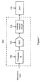
- FIG. 1 depicts a simplified, high-level block diagram of an arbitrary waveform generator according to a first embodiment of the present invention.
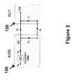
- FIG. 2 depicts a first signal flow graph that corresponds to FIG. 1 .
- FIG. 3 depicts a second signal flow graph that corresponds to FIG. 1 .
- FIG. 4 depicts a method that corresponds to FIG. 1 .
- FIG. 5 depicts a simplified, high-level block diagram of an arbitrary waveform generator according to a second embodiment of the present invention.
- FIG. 6 depicts a first signal flow graph that corresponds to FIG. 5 .
- FIG. 7 depicts a second signal flow graph that corresponds to FIG. 5 .
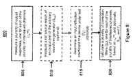
- FIG. 8 depicts a method that corresponds to FIG. 5 .
- AWGs appear to have imperfect output responses because prior AWG calibration techniques have not taken into account the interaction of reflected waves between the AWG and the measurement instrument during calibration, or between the AWG and the device under test (DUT) during use.
- embodiments of the present invention provide methods of calibrating a channel of an AWG, and arbitrary waveform generators calibrated according to those methods, that take into account not only the output response of the channel, but also the interaction of reflected waves between the AWG and a measurement instrument during calibration, and between the AWG and the DUT during use.
- FIG. 1 depicts an AWG 100 having a single, non-interleaved channel according to an embodiment of the present invention.
- a processor 105 receives waveform data that describes a desired output analog signal.
- the waveform data may be received from a memory, a storage device, or the like.
- the processor 105 may be implemented as software running on a general-purpose microprocessor, a dedicated application specific integrated circuit (ASIC), a field programmable gate array (FPGA), or the like.
- the processor 105 applies a correction filter g to the waveform data in order to correct the output response of the channel.
- the correction filter g can be applied to the waveform data by convolving the correction filter g with the waveform data in the time domain, or by multiplying them together in the frequency domain.
- the processed waveform data is converted into an analog signal using a digital-to-analog converter (DAC) 110.
- the analog signal is filtered by an analog output circuit 115, which may include an amplifier, an attenuator, a switch, a reconstruction filter, and the like.
- the filtered analog signal is then applied to a DUT 120.
- the single, non-interleaved channel refers to the signal path from the DAC 110 through the analog output circuit 115.
- the DAC 110 provides a differential output. In that case, the two outputs may be considered either a pair of channels or a single differential channel.
- the correction filter g is calculated as follows:
- the output response (amplitude and phase) of the channel is measured with a calibrated measurement instrument such as a sampling oscilloscope.
- the source match, or reflection coefficient, is measured with a calibrated measurement instrument such as a time-domain reflectometer (TDR) or a network analyzer.
- TDR time-domain reflectometer
- ⁇ and ⁇ s are written as ⁇ and ⁇ s respectively.
- S 11s and S 12s equal zero because the input of the DAC is digital in nature, not analog, and thus, no digital data applied to its input can reflect back, and no analog signal applied to its output can pass through to its input.
- Equation 3 Substituting Equation 3 into Equation 2 yields:
- b Z a s ⁇ g ⁇ + b Z ⁇ ⁇ L ⁇ ⁇ s
- Equation 5 Substituting Equation 5 into Equation 3 yields:
- b 2 a s ⁇ g ⁇ ⁇ ⁇ L 1 - ⁇ L ⁇ ⁇ s
- a calibrated measurement instrument is defined as an instrument that correctly measures the phase and amplitude of the incoming wave from a matched 50 ohm source. Its input is not necessarily matched, and has an input reflection coefficient ⁇ L .
- a calibrated AWG is defined as an AWG that produces an accurate waveform into a matched 50 ohm load and has an output reflection coefficient ⁇ s . In that case, Equation 5 reduces to:
- ⁇ b Z ⁇ meas a s ⁇ 1 - ⁇ L ⁇ ⁇ s
- Equation 11 Substituting Equation 11 into Equation 9 yields:
- g matc k represents the correction filter assuming a matched load
- ⁇ LDUT represents the input reflection coefficient of the DUT
- ⁇ s represents the output reflection coefficient of the AWG.
- the DUT input reflection coefficient is an ideal, calculated value, selected so that the correction filter corrects the output response so that it is right when working into a matched 50 ohm load, an open circuit, or any other specified impedance.
- This correction filter can be generated during manufacturing, stored in the AWG, and used when the DUT s-parameters are not available.
- the DUT input reflection coefficient is a measured value by the user, in which case the correction filter corrects the output response so that it is right when working into the DUT.
- the AWG shown and described above only has a single, non-interleaved channel
- this same calibration approach can also be used to improve the output response of an AWG having multiple interleaved channels. That is, the output response of an interleaved AWG can be improved by taking into account the interaction of reflected waves between the AWG and the measurement instrument during calibration, and between the AWG and the DUT during use.
- the correction filter g developed above can be used as-is, provided that the multiple interleaved channels are treated as a single higher rate non-interleaved channel, and the source match of the channel ( ⁇ s ) equals the net source match of the arbitrary waveform generator (S net ), described in detail below.
- the correction filter g is essentially the same as described above. This is because, when the s-parameters of the external device 125 are cascaded with the source parameters, the form of the new effective source output remains the same because of the two zeros in the first row of the source matrix.
- the shifted source parameters can be measured directly with the external device 125 in place or calculated using known front panel referenced AWG 100 parameters and external device parameters.
- FIG. 4 depicts a method 400 of calibrating a channel of an arbitrary waveform generator according to an embodiment of the present invention.
- step 405 an output response of the channel is measured ( ⁇ ).
- step 410 a source match of the channel is measured ( ⁇ s ).
- step 415 an input reflection coefficient of a DUT is determined ( ⁇ L ).
- step 420 a correction filter (g) for the channel is calculated based on ⁇ , ⁇ s , and ⁇ L . Steps 405, 410, and 415 are not required to be performed in the order shown, but rather can be performed in any order.
- AWGs achieve higher samples rate by interleaving multiple channels together. However, when doing so, the resulting output response is more difficult to correct for several reasons. The first reason is that the individual output responses of the interleaved channels will not match, and thus a single correction filter cannot be completely right. The second reason is that the overall output response will be influenced by reflections between the multiple sources, as well as reflections between the multiple sources and the DUT.
- embodiments of the present invention provide methods of calibrating multiple interleaved channels of an AWG, and arbitrary waveform generators calibrated according to those methods, that take into account the output response of each interleaved channel, the interaction of reflected waves between the AWG and a measurement instrument during calibration and between the AWG and the DUT during use, or both simultaneously. For reasons that will be explained below, these methods correct the output response of each channel independently, and apply the correction filter to the lower sample rate waveform input to each DAC rather than the full sample rate waveform.
- FIG. 5 depicts an AWG 500 having two interleaved channels according to an embodiment of the present invention.
- the AWG 500 is similar to the AWG 100, except that it includes two DACs 510A and 510B instead of a single DAC 100, and a combiner 530.
- the two DACs 510A and 510B are clocked by two clock signals (not shown) that are phase shifted relative to one another by 180 degrees.
- the processor 505 separates the waveform data into samples for the first channel and samples for the second channel, and then applies a first correction filter g 1 to the samples for the first channel, and applies a second correction filter g 2 to the samples for the second channel.
- g 1 and g 2 correct the output responses of the first and second interleaved channels, respectively, and also take into account the interaction of reflected waves between the AWG 500 and a measurement instrument during calibration, and between the AWG 500 and the DUT 120 during use.
- the DAC 510A converts the samples for the first channel into a first analog signal
- the DAC 510B converts the samples for the second channel into a second analog signal.
- the first and second analog signals are then combined into a single analog signal with the combiner 530, which is any device used to combine analog signals.
- the resulting analog signal has double the sample rate of either of the individual DACs 510A and 510B.
- the combined analog signal is then filtered with an analog output circuit 115 and applied to a DUT 120.
- the first interleaved channel refers to the signal path from the processor 505 through the DAC 510A to the analog output circuit 115
- the second interleaved channel refers to the signal path from the processor 505 through the DAC 510B to the analog output circuit 115.
- the correction filters g 1 and g 2 are developed as follows:
- the combiner 530 can be any device used to combine analog signals. However, in the following discussion, the combiner 530 is considered to be a symmetric, resistive power combiner. Thus, referring now to FIG. 6 , the combiner 530 can be represented by a 3 ⁇ 3 s-parameter matrix:
- Equations 16 and 17 become:
- the two source ports are idealized; there are no reflections between the sources and the effective combiner, meaning that s 11 and s 22 are zero; and, returning waves b 1 ⁇ and b 2 ⁇ are zero, meaning that s 12 , s 13 , s 21 , and s 23 are all zero.
- ⁇ 1 net and ⁇ 2 net are the output responses of the two sources measured through the effective combiner.
- ⁇ 1 net and ⁇ 2 net are measured "independently,” that is, the individual output response of DAC 510A is measured with DAC 510B set to zero, and the individual output response of DAC510B is measured with DAC510A set to zero.
- Equation 23 Substituting Equation 23 into Equation 22 yields:
- Equation 25 is the sum of the response from each channel modified by reflections between the output port and load. It is identical to Equation 5 for the single channel case, except that the source transmission is the sum of two sources.
- the source waveform can be compensated to correct for it. This part of the correction can be included in a total filter for each DAC or applied to the starting waveform at the full sample rate, since it is the same for both DACs.
- correction filters g 1 and g 2 are as follows:
- g 1 g matck ⁇ 1 ⁇ g refl
- g matc k1 and g matc k2 represent the first and second correction filters assuming a matched load.
- correction filters can be generated for systems having three interleaved channels, four interleaved channels, and so on.
- g 1 , g 2 , and so on are collectively referred to as g n
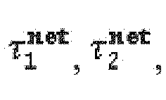
- ⁇ 1 net , ⁇ 2 net , and so on are collectively referred to as ⁇ n net .
- correction filters can also be generated that only take into account the individual output responses of the interleaved channels. That is, in some embodiments, an arbitrary waveform generator is calibrated by measuring the output response of each interleaved channel independently and then generating a plurality of correction filters, one for each interleaved channel, based solely on its corresponding measured output response. In that case, each correction filter equals the inverse of its associated measured output response. In other embodiments, the DUT input reflection coefficient and the net source match of the AWG are also measured and used to improve the accuracy of those correction filters.
- FIG. 8 depicts a method 800 of calibrating a plurality of interleaved channels of an arbitrary waveform generator according to an embodiment of the present invention.
- step 805 a plurality of output responses, one for each of the plurality of interleaved channels is measured ( ⁇ n net ).
- step 810 a net source match of an output port of the arbitrary waveform generator is measured (S net ).
- step 815 an input reflection coefficient of a device under test is determined ( ⁇ L )
- a plurality of correction filters (g n ) are calculated, one for each of the plurality of interleaved channels, based on ⁇ n net , S net , and ⁇ L . Steps 805, 810, and 815 are not required to be performed in the order shown, but rather can be performed in any order.
- pairs of channels are used to generate differential signals, both pairs of single, non-interleaved channels and pairs of multiple interleaved channels.
- Each of those channels can be individually calibrated using the techniques described above.
- the pairs of channels can be calibrated simultaneously using the techniques described above by replacing the single-ended parameters with differential parameters. That is, the single-ended output response of a channel ( ⁇ ) would be replaced with the differential output response of a pair of single-ended, non-interleaved channels, or the differential output response of a pair of multiple interleaved channels, and so on.
Landscapes
- Engineering & Computer Science (AREA)
- General Engineering & Computer Science (AREA)
- Physics & Mathematics (AREA)
- General Physics & Mathematics (AREA)
- Measurement Of Resistance Or Impedance (AREA)
- Tests Of Electronic Circuits (AREA)
Abstract
Description
- The present invention relates to test and measurement instruments, and more particularly to the calibration of arbitrary waveform generators.
- Arbitrary Waveform Generators (AWGs) are test and measurement instruments that are used to generate analog signals having virtually any waveshape. In operation, a user defines a desired analog signal point-by-point as a series of digital values. An AWG then "plays out" the digital values using a precision digital-to-analog converter to provide the analog signal. AWGs such as the AWG7000 Arbitrary Waveform Generator Series available from Tektronix, Inc. of Beaverton, Oregon are used for wideband signal generation applications, receiver stress testing of high-speed serial data, and other applications where complex signal creation is required.
- For various reasons, the measured frequency characteristics of signals produced by AWGs sometimes differ from the frequency characteristics of their input waveform data. Calibration techniques have been proposed to correct the output responses of AWGs, however, none of them has proven entirely satisfactory.
- Thus, there exists a need for enhanced methods of calibrating AWGs.
- Embodiments of the present invention provide enhanced methods of calibrating arbitrary waveform generators using s-parameters, and arbitrary waveform generators calibrated according to those methods. Methods are provided for calibrating a single, non-interleaved channel of an arbitrary waveform generator, calibrating multiple interleaved channels, and calibrating pairs of channels, both interleaved and non-interleaved, to generate differential signals.
- The objects, advantages, and other novel features of the present invention are apparent from the following detailed description when read in conjunction with the appended claims and attached drawings.
-
FIG. 1 depicts a simplified, high-level block diagram of an arbitrary waveform generator according to a first embodiment of the present invention. -
FIG. 2 depicts a first signal flow graph that corresponds toFIG. 1 . -
FIG. 3 depicts a second signal flow graph that corresponds toFIG. 1 . -
FIG. 4 depicts a method that corresponds toFIG. 1 . -
FIG. 5 depicts a simplified, high-level block diagram of an arbitrary waveform generator according to a second embodiment of the present invention. -
FIG. 6 depicts a first signal flow graph that corresponds toFIG. 5 . -
FIG. 7 depicts a second signal flow graph that corresponds toFIG. 5 . -
FIG. 8 depicts a method that corresponds toFIG. 5 . - 1. Accounting for Reflected Waves
- The inventor has recognized that AWGs appear to have imperfect output responses because prior AWG calibration techniques have not taken into account the interaction of reflected waves between the AWG and the measurement instrument during calibration, or between the AWG and the device under test (DUT) during use.
- Accordingly, embodiments of the present invention provide methods of calibrating a channel of an AWG, and arbitrary waveform generators calibrated according to those methods, that take into account not only the output response of the channel, but also the interaction of reflected waves between the AWG and a measurement instrument during calibration, and between the AWG and the DUT during use.
-
FIG. 1 depicts an AWG 100 having a single, non-interleaved channel according to an embodiment of the present invention. In operation, aprocessor 105 receives waveform data that describes a desired output analog signal. The waveform data may be received from a memory, a storage device, or the like. Theprocessor 105 may be implemented as software running on a general-purpose microprocessor, a dedicated application specific integrated circuit (ASIC), a field programmable gate array (FPGA), or the like. Theprocessor 105 applies a correction filter g to the waveform data in order to correct the output response of the channel. The correction filter g can be applied to the waveform data by convolving the correction filter g with the waveform data in the time domain, or by multiplying them together in the frequency domain. The processed waveform data is converted into an analog signal using a digital-to-analog converter (DAC) 110. The analog signal is filtered by ananalog output circuit 115, which may include an amplifier, an attenuator, a switch, a reconstruction filter, and the like. The filtered analog signal is then applied to aDUT 120. "The single, non-interleaved channel" refers to the signal path from theDAC 110 through theanalog output circuit 115. In some embodiments (not shown), theDAC 110 provides a differential output. In that case, the two outputs may be considered either a pair of channels or a single differential channel. - In some embodiments, the correction filter g is calculated as follows:
- Referring now to
FIG. 2 , the output response (amplitude and phase) of the channel is measured with a calibrated measurement instrument such as a sampling oscilloscope. The source match, or reflection coefficient, is measured with a calibrated measurement instrument such as a time-domain reflectometer (TDR) or a network analyzer. Together, they form the s-parameters of the source S21s and S22s. For clarity later in the analysis, these are written as τ and Γs respectively. -

- S11s and S12s equal zero because the input of the DAC is digital in nature, not analog, and thus, no digital data applied to its input can reflect back, and no analog signal applied to its output can pass through to its input.
- To complete the analysis, the DUT input reflection coefficient (ΓL) must be known. Then, the response equations can be written:
-

-

- Substituting Equation 3 into Equation 2 yields:
-

- Rearranging Equation 4 to solve for b2 yields:
-

- Substituting Equation 5 into Equation 3 yields:
-

- A. Calibration
- A calibrated measurement instrument is defined as an instrument that correctly measures the phase and amplitude of the incoming wave from a matched 50 ohm source. Its input is not necessarily matched, and has an input reflection coefficient Γ L . Similarly, a calibrated AWG is defined as an AWG that produces an accurate waveform into a matched 50 ohm load and has an output reflection coefficient Γ s . In that case, Equation 5 reduces to:
-

- And:
-

- Therefore:
-

- However, when the calibrated instrument and the source are put together (with g = 1), the measured result is:
-

- Rearranging Equation 10 yields:
-

- Substituting Equation 11 into Equation 9 yields:
-

- B. Driving a DUT
- Now, when a new device is driven with the calibrated source, the resulting forward wave is:
-

- Lastly, the DUT input reflection coefficient must be taken into account. The desired output is just asg matc k τ , so the correction filter g is:
-

- Where g matc k represents the correction filter assuming a matched load, Γ LDUT represents the input reflection coefficient of the DUT, and Γ s represents the output reflection coefficient of the AWG.
- In some embodiments, the DUT input reflection coefficient is an ideal, calculated value, selected so that the correction filter corrects the output response so that it is right when working into a matched 50 ohm load, an open circuit, or any other specified impedance. This correction filter can be generated during manufacturing, stored in the AWG, and used when the DUT s-parameters are not available. In other embodiments, the DUT input reflection coefficient is a measured value by the user, in which case the correction filter corrects the output response so that it is right when working into the DUT.
- Although the AWG shown and described above only has a single, non-interleaved channel, it will be appreciated that this same calibration approach can also be used to improve the output response of an AWG having multiple interleaved channels. That is, the output response of an interleaved AWG can be improved by taking into account the interaction of reflected waves between the AWG and the measurement instrument during calibration, and between the AWG and the DUT during use. In that case, the correction filter g developed above can be used as-is, provided that the multiple interleaved channels are treated as a single higher rate non-interleaved channel, and the source match of the channel (Γs) equals the net source match of the arbitrary waveform generator (Snet), described in detail below.
- C. Adding an External Device
- Referring now to
FIG. 3 , when anexternal device 125 such as a cable, an up-converter, or the like is used between theAWG 100 and theDUT 120, it can be more appropriate to calibrate at the output of theexternal device 125. In that case, the correction filter g is essentially the same as described above. This is because, when the s-parameters of theexternal device 125 are cascaded with the source parameters, the form of the new effective source output remains the same because of the two zeros in the first row of the source matrix. The shifted source parameters can be measured directly with theexternal device 125 in place or calculated using known front panel referencedAWG 100 parameters and external device parameters. -
FIG. 4 depicts amethod 400 of calibrating a channel of an arbitrary waveform generator according to an embodiment of the present invention. Instep 405, an output response of the channel is measured (τ). Instep 410, a source match of the channel is measured (Γs). Instep 415, an input reflection coefficient of a DUT is determined (ΓL). Instep 420, a correction filter (g) for the channel is calculated based on τ, Γs, and ΓL.Steps - 2. Correcting Multiple Interleaved Channels
- Many AWGs achieve higher samples rate by interleaving multiple channels together. However, when doing so, the resulting output response is more difficult to correct for several reasons. The first reason is that the individual output responses of the interleaved channels will not match, and thus a single correction filter cannot be completely right. The second reason is that the overall output response will be influenced by reflections between the multiple sources, as well as reflections between the multiple sources and the DUT.
- Accordingly, embodiments of the present invention provide methods of calibrating multiple interleaved channels of an AWG, and arbitrary waveform generators calibrated according to those methods, that take into account the output response of each interleaved channel, the interaction of reflected waves between the AWG and a measurement instrument during calibration and between the AWG and the DUT during use, or both simultaneously. For reasons that will be explained below, these methods correct the output response of each channel independently, and apply the correction filter to the lower sample rate waveform input to each DAC rather than the full sample rate waveform.
-
FIG. 5 depicts anAWG 500 having two interleaved channels according to an embodiment of the present invention. TheAWG 500 is similar to theAWG 100, except that it includes twoDACs single DAC 100, and acombiner 530. The twoDACs processor 505 separates the waveform data into samples for the first channel and samples for the second channel, and then applies a first correction filter g1 to the samples for the first channel, and applies a second correction filter g2 to the samples for the second channel. g1 and g2 correct the output responses of the first and second interleaved channels, respectively, and also take into account the interaction of reflected waves between theAWG 500 and a measurement instrument during calibration, and between theAWG 500 and theDUT 120 during use. TheDAC 510A converts the samples for the first channel into a first analog signal, and theDAC 510B converts the samples for the second channel into a second analog signal. The first and second analog signals are then combined into a single analog signal with thecombiner 530, which is any device used to combine analog signals. The resulting analog signal has double the sample rate of either of theindividual DACs AWG 100, the combined analog signal is then filtered with ananalog output circuit 115 and applied to aDUT 120. "The first interleaved channel" refers to the signal path from theprocessor 505 through theDAC 510A to theanalog output circuit 115, and "the second interleaved channel" refers to the signal path from theprocessor 505 through theDAC 510B to theanalog output circuit 115. - In some embodiments, the correction filters g1 and g2 are developed as follows:
- The
combiner 530 can be any device used to combine analog signals. However, in the following discussion, thecombiner 530 is considered to be a symmetric, resistive power combiner. Thus, referring now toFIG. 6 , thecombiner 530 can be represented by a 3×3 s-parameter matrix: -

- In matrix notation, the s-parameter equation is:
-

- Where:
-

- The solution for the output taking into account the source parameters and the combiner is developed in the Appendix.
-

- The difficulty with this approach, however, is that the solution requires knowledge of the details of the reflection and transmission parameters of each channel, along with the two internal ports of the combiner. However, it is very difficult to directly measure individual parameters once the instrument is assembled. If they can be determined at all, it would only be through a complex set of calibration measurements and calculations because the response can only be observed at the output.
- On the other hand, if the AWG is viewed from the perspective of the single output port, then the details of the internal interactions are not important. This perspective is depicted in
FIG. 7 , where the output wave is the sum of the response from each channel to the output, and theDUT 120 interacts with a net single port reflection coefficient at the output port. An overall net three port s-parameter network can be considered to include the DAC outputs, the interconnect, and the combiner. With this simplification, Equations 16 and 17 become: -

-

- The two source ports are idealized; there are no reflections between the sources and the effective combiner, meaning that s11 and s22 are zero; and, returning
waves 

-

- Where


DAC 510A is measured withDAC 510B set to zero, and the individual output response of DAC510B is measured with DAC510A set to zero. - We are left with an equation for b3 dependent on the two source waves and the reflection from the load, a3:
-

-

- Substituting Equation 23 into
Equation 22 yields: -

- Rearranging yields:
-

- Equation 25 is the sum of the response from each channel modified by reflections between the output port and load. It is identical to Equation 5 for the single channel case, except that the source transmission is the sum of two sources.
- A. Calibration
- Now, when working into a matched load, the output is:
-

- If the output from each DAC is measured independently with the other DAC set to zero, then the two correction factors are:
-

-

- Finally, the output of the calibrated source is:
-

- B. Driving a DUT
- Like the single channel case, if the DUT reflection coefficient is known, then the source waveform can be compensated to correct for it. This part of the correction can be included in a total filter for each DAC or applied to the starting waveform at the full sample rate, since it is the same for both DACs.
-

- Where:
-

- Thus, the correction filters g1 and g2 are as follows:
-

-

- Where g matc k1 and g matc k2 represent the first and second correction filters assuming a matched load.
- Although the discussion above describes generating two correction filters for a system having two interleaved channels, it will be appreciated that, by applying similar reasoning, additional correction filters can also be developed for systems using higher degrees of interleaving. That is, correction filters can be generated for systems having three interleaved channels, four interleaved channels, and so on. In that case, to generalize the notation for an arbitrary number of interleaved channels, g1, g2, and so on are collectively referred to as gn, and

- Also, although the correction filters described above simultaneously take into account both the individual output responses of the interleaved channels and the effects of reflections between the DUT and the multiple sources at the same time, correction filters can also be generated that only take into account the individual output responses of the interleaved channels. That is, in some embodiments, an arbitrary waveform generator is calibrated by measuring the output response of each interleaved channel independently and then generating a plurality of correction filters, one for each interleaved channel, based solely on its corresponding measured output response. In that case, each correction filter equals the inverse of its associated measured output response. In other embodiments, the DUT input reflection coefficient and the net source match of the AWG are also measured and used to improve the accuracy of those correction filters.
-
FIG. 8 depicts amethod 800 of calibrating a plurality of interleaved channels of an arbitrary waveform generator according to an embodiment of the present invention. Instep 805, a plurality of output responses, one for each of the plurality of interleaved channels is measured (τn net). Optionally, instep 810, a net source match of an output port of the arbitrary waveform generator is measured (Snet). Optionally, instep 815, an input reflection coefficient of a device under test is determined (ΓL) Instep 820, a plurality of correction filters (gn) are calculated, one for each of the plurality of interleaved channels, based on τn net, Snet, and ΓL.Steps - 3. Correcting Pairs of Channels Used to Generate Differential Signals
- In some cases, pairs of channels are used to generate differential signals, both pairs of single, non-interleaved channels and pairs of multiple interleaved channels. Each of those channels can be individually calibrated using the techniques described above. Alternatively, the pairs of channels can be calibrated simultaneously using the techniques described above by replacing the single-ended parameters with differential parameters. That is, the single-ended output response of a channel (τ) would be replaced with the differential output response of a pair of single-ended, non-interleaved channels, or the differential output response of a pair of multiple interleaved channels, and so on.
- It will be appreciated from the foregoing discussion that the present invention represents a significant advance in the field of test and measurement instruments. Although specific embodiments of the invention have been illustrated and described for purposes of illustration, it will be understood that various modifications may be made without deporting from the spirit and scope of the invention. Accordingly, the invention should not be limited except as by the appended claims.


Claims (7)
- A method of calibrating a plurality of interleaved channels of an arbitrary waveform generator comprising the steps of:measuring a plurality of output responses, one for each of the plurality of interleaved channels (τn net); andcalculating a plurality of correction filters (gn), one for each of the plurality of interleaved channels, based on τn net.
- A method as in claim 1 further comprising the steps of:measuring a net source match of an output port of the arbitrary waveform generator (Snet); anddetermining an input reflection coefficient of a device under test (ΓL);and wherein the plurality of correction filters (gn) are calculated based on τn net, Snet, and ΓL.
- A method as in claim 1 wherein each of the plurality of interleaved channels comprises a differential channel.
- A method as in claim 2 wherein ΓL is an ideal, calculated value.
- A method as in claim 2 wherein ΓL is a measured value.
- A method as in claim 1 wherein:an external device is connected to an output port of the arbitrary waveform generator; andthe calibration is performed at an output port of the external device.
- An arbitrary waveform generator calibrated according to the method of any one of claims 1-6.
Applications Claiming Priority (1)
| Application Number | Priority Date | Filing Date | Title |
|---|---|---|---|
| US13/243,163 US9927485B2 (en) | 2011-09-23 | 2011-09-23 | Enhanced AWG waveform calibration using S-parameters |
Publications (1)
| Publication Number | Publication Date |
|---|---|
| EP2574943A1 true EP2574943A1 (en) | 2013-04-03 |
Family
ID=47071106
Family Applications (1)
| Application Number | Title | Priority Date | Filing Date |
|---|---|---|---|
| EP12183019A Withdrawn EP2574943A1 (en) | 2011-09-23 | 2012-09-04 | Enhanced arbitrary waveform generator waveform calibration using s-parameters |
Country Status (4)
| Country | Link |
|---|---|
| US (1) | US9927485B2 (en) |
| EP (1) | EP2574943A1 (en) |
| JP (1) | JP2013068619A (en) |
| CN (1) | CN103018700B (en) |
Families Citing this family (6)
| Publication number | Priority date | Publication date | Assignee | Title |
|---|---|---|---|---|
| US20130080105A1 (en) * | 2011-09-23 | 2013-03-28 | Tektronix, Inc | Enhanced awg wavef0rm calibration using s-parameters |
| CN104572388B (en) * | 2013-10-15 | 2017-01-25 | 鸿富锦精密工业(深圳)有限公司 | Data filtering system, data filtering device and method |
| CN106405463B (en) * | 2016-09-05 | 2019-01-22 | 中国计量科学研究院 | Measurement Method of Reflection Coefficient of Calibration Signal Source in Microwave Power Meter |
| US10901017B2 (en) * | 2017-08-09 | 2021-01-26 | Nvidia Corporation | Systematic methodology to remove reflections from I/O measurements |
| CN108020803B (en) * | 2017-11-21 | 2019-09-24 | 中国电子科技集团公司第四十一研究所 | A kind of arbitrary waveform generator amplitude frequency sweep estimation calibration method |
| US10732222B2 (en) * | 2018-03-29 | 2020-08-04 | Rohde & Schwarz Gmbh & Co. Kg | Real-time oscilloscope with a built-in time domain reflectometry (TDR) and/or time-domain transmission (TDT) function |
Citations (5)
| Publication number | Priority date | Publication date | Assignee | Title |
|---|---|---|---|---|
| DE19723087A1 (en) * | 1996-08-01 | 1998-02-05 | Hewlett Packard Co | Error correction method for transmission measurements in vector network analyzers |
| US20080265911A1 (en) * | 2008-07-14 | 2008-10-30 | Agilent Technologies, Inc. | Power Sensing Module with Built-In Mismatch and Correction |
| JP2008286699A (en) * | 2007-05-18 | 2008-11-27 | Advantest Corp | Signal input and output device, testing device, and electronic device |
| US20090052556A1 (en) * | 2007-08-23 | 2009-02-26 | Fernandez Andrew D | Frequency interleaving method for wideband signal generation |
| US20090195498A1 (en) * | 2008-02-01 | 2009-08-06 | Tektronix International Sales Gmbh | Signal Generator Providing ISI Scaling to Touchstone Files |
Family Cites Families (8)
| Publication number | Priority date | Publication date | Assignee | Title |
|---|---|---|---|---|
| US6801042B2 (en) * | 2001-12-18 | 2004-10-05 | Tektronix, Inc. | Calibration method and apparatus for signal analysis device |
| JP2007027921A (en) * | 2005-07-13 | 2007-02-01 | Agilent Technol Inc | Method for adjusting signal generator and signal generator |
| US7256585B1 (en) * | 2006-07-21 | 2007-08-14 | Agilent Technologies, Inc. | Match-corrected power measurements with a vector network analyzer |
| US7405575B2 (en) * | 2006-08-23 | 2008-07-29 | Tektronix, Inc. | Signal analysis system and calibration method for measuring the impedance of a device under test |
| US7873980B2 (en) * | 2006-11-02 | 2011-01-18 | Redmere Technology Ltd. | High-speed cable with embedded signal format conversion and power control |
| JP5224708B2 (en) * | 2007-03-28 | 2013-07-03 | 株式会社東芝 | Acoustic signal generating apparatus and method |
| WO2009090825A1 (en) * | 2008-01-15 | 2009-07-23 | Mitsubishi Electric Corporation | Predistorter |
| JP2011228815A (en) | 2010-04-15 | 2011-11-10 | Tektronix Inc | Frequency characteristic correction method for arbitrary waveform generator |
-
2011
- 2011-09-23 US US13/243,163 patent/US9927485B2/en not_active Expired - Fee Related
-
2012
- 2012-09-04 EP EP12183019A patent/EP2574943A1/en not_active Withdrawn
- 2012-09-21 CN CN201210371145.3A patent/CN103018700B/en not_active Expired - Fee Related
- 2012-09-24 JP JP2012209440A patent/JP2013068619A/en not_active Ceased
Patent Citations (5)
| Publication number | Priority date | Publication date | Assignee | Title |
|---|---|---|---|---|
| DE19723087A1 (en) * | 1996-08-01 | 1998-02-05 | Hewlett Packard Co | Error correction method for transmission measurements in vector network analyzers |
| JP2008286699A (en) * | 2007-05-18 | 2008-11-27 | Advantest Corp | Signal input and output device, testing device, and electronic device |
| US20090052556A1 (en) * | 2007-08-23 | 2009-02-26 | Fernandez Andrew D | Frequency interleaving method for wideband signal generation |
| US20090195498A1 (en) * | 2008-02-01 | 2009-08-06 | Tektronix International Sales Gmbh | Signal Generator Providing ISI Scaling to Touchstone Files |
| US20080265911A1 (en) * | 2008-07-14 | 2008-10-30 | Agilent Technologies, Inc. | Power Sensing Module with Built-In Mismatch and Correction |
Non-Patent Citations (2)
| Title |
|---|
| ANONYMOUS: "Creating Calibrated UWB WiMedia Signals, Application Note", 2008, Online, pages 1 - 12, XP002692222, Retrieved from the Internet <URL:http://www.tek.com/document/application-note/creating-calibrated-uwb-wimedia-signals> [retrieved on 20130108] * |
| JOAN MERCADÉ: "DAC Interleaving in Ultra-High-Speed Arbs", EVALUATION ENGINEERING, December 2009 (2009-12-01), Online, pages 14 - 22, XP002690094, Retrieved from the Internet <URL:http://www.arbitrary.es/Files/EE_hs_arbs.pdf> [retrieved on 20130108] * |
Also Published As
| Publication number | Publication date |
|---|---|
| US9927485B2 (en) | 2018-03-27 |
| JP2013068619A (en) | 2013-04-18 |
| CN103018700B (en) | 2018-03-30 |
| US20130080106A1 (en) | 2013-03-28 |
| CN103018700A (en) | 2013-04-03 |
Similar Documents
| Publication | Publication Date | Title |
|---|---|---|
| EP2574942A1 (en) | Enhanced arbitrary waveform generator waveform calibration using s-parameters | |
| US7739063B2 (en) | Nonlinear measurement system error correction | |
| US9927485B2 (en) | Enhanced AWG waveform calibration using S-parameters | |
| US10901044B2 (en) | Apparatuses and methods for testing electrochemical cells by measuring frequency response | |
| US8706438B2 (en) | Time domain network analyzer | |
| CN1673768B (en) | Calibration method and apparatus | |
| US7660685B2 (en) | Virtual probing | |
| Blockley et al. | Mixer-based, vector-corrected, vector signal/network analyzer offering 300kHz-20GHz bandwidth and traceable phase response | |
| US8860434B2 (en) | Method of measuring scattering parameters of device under test | |
| US10145874B2 (en) | S-parameter measurements using real-time oscilloscopes | |
| US20110286506A1 (en) | User Interface for Signal Integrity Network Analyzer | |
| US7538708B2 (en) | Efficient, selective error reduction for parallel, time-interleaved analog-to-digital converter | |
| US20070276614A1 (en) | De-embed method for multiple probes coupled to a device under test | |
| US20110191046A1 (en) | Time domain reflectometry step to s-parameter conversion | |
| US7541958B2 (en) | Error reduction for parallel, time-interleaved analog-to-digital converter | |
| US20110234239A1 (en) | Two-Port De-Embedding Using Time Domain Substitution | |
| CN104777370A (en) | Automatic fixture removal using one-port measurement | |
| US9413404B2 (en) | Method and system for characterising a frequency translating device | |
| JP2006105984A (en) | Method and apparatus for measuring a digital device | |
| US20250271492A1 (en) | Measurement system for active load pull testing and active load pull measurement method | |
| US10451453B2 (en) | System and method for calibrating a measuring arrangement and characterizing a measurement mount | |
| US12487264B2 (en) | Signal processing circuit and measurement system | |
| Barmuta et al. | Comparing LSNA calibrations: Large-signal network analyzer round robin | |
| CN108872906A (en) | A kind of method and system for demarcating tested sensor linearity using the continuous quantity of electric charge | |
| Azhar | Large Signal RF Measurement Systems and Implementation of a Tuned Receiver System |
Legal Events
| Date | Code | Title | Description |
|---|---|---|---|
| PUAI | Public reference made under article 153(3) epc to a published international application that has entered the european phase |
Free format text: ORIGINAL CODE: 0009012 |
|
| AK | Designated contracting states |
Kind code of ref document: A1 Designated state(s): AL AT BE BG CH CY CZ DE DK EE ES FI FR GB GR HR HU IE IS IT LI LT LU LV MC MK MT NL NO PL PT RO RS SE SI SK SM TR |
|
| AX | Request for extension of the european patent |
Extension state: BA ME |
|
| 17P | Request for examination filed |
Effective date: 20131003 |
|
| RBV | Designated contracting states (corrected) |
Designated state(s): AL AT BE BG CH CY CZ DE DK EE ES FI FR GB GR HR HU IE IS IT LI LT LU LV MC MK MT NL NO PL PT RO RS SE SI SK SM TR |
|
| RAP1 | Party data changed (applicant data changed or rights of an application transferred) |
Owner name: TEKTRONIX, INC. |
|
| 17Q | First examination report despatched |
Effective date: 20180502 |
|
| STAA | Information on the status of an ep patent application or granted ep patent |
Free format text: STATUS: THE APPLICATION IS DEEMED TO BE WITHDRAWN |
|
| 18D | Application deemed to be withdrawn |
Effective date: 20180913 |