EP2571256A1 - Exposure controlling apparatus and method of imaging element, and imaging apparatus - Google Patents
Exposure controlling apparatus and method of imaging element, and imaging apparatus Download PDFInfo
- Publication number
- EP2571256A1 EP2571256A1 EP20120181571 EP12181571A EP2571256A1 EP 2571256 A1 EP2571256 A1 EP 2571256A1 EP 20120181571 EP20120181571 EP 20120181571 EP 12181571 A EP12181571 A EP 12181571A EP 2571256 A1 EP2571256 A1 EP 2571256A1
- Authority
- EP
- European Patent Office
- Prior art keywords
- exposure amount
- exposure
- imaging element
- error
- optimum
- Prior art date
- Legal status (The legal status is an assumption and is not a legal conclusion. Google has not performed a legal analysis and makes no representation as to the accuracy of the status listed.)
- Granted
Links
Images



Classifications
-
- H—ELECTRICITY
- H04—ELECTRIC COMMUNICATION TECHNIQUE
- H04N—PICTORIAL COMMUNICATION, e.g. TELEVISION
- H04N5/00—Details of television systems
- H04N5/44—Receiver circuitry for the reception of television signals according to analogue transmission standards
- H04N5/57—Control of contrast or brightness
-
- G—PHYSICS
- G03—PHOTOGRAPHY; CINEMATOGRAPHY; ANALOGOUS TECHNIQUES USING WAVES OTHER THAN OPTICAL WAVES; ELECTROGRAPHY; HOLOGRAPHY
- G03B—APPARATUS OR ARRANGEMENTS FOR TAKING PHOTOGRAPHS OR FOR PROJECTING OR VIEWING THEM; APPARATUS OR ARRANGEMENTS EMPLOYING ANALOGOUS TECHNIQUES USING WAVES OTHER THAN OPTICAL WAVES; ACCESSORIES THEREFOR
- G03B7/00—Control of exposure by setting shutters, diaphragms or filters, separately or conjointly
- G03B7/08—Control effected solely on the basis of the response, to the intensity of the light received by the camera, of a built-in light-sensitive device
- G03B7/099—Arrangement of photoelectric elements in or on the camera
- G03B7/0993—Arrangement of photoelectric elements in or on the camera in the camera
- G03B7/0997—Through the lens [TTL] measuring
- G03B7/09979—Multi-zone light measuring
-
- H—ELECTRICITY
- H04—ELECTRIC COMMUNICATION TECHNIQUE
- H04N—PICTORIAL COMMUNICATION, e.g. TELEVISION
- H04N23/00—Cameras or camera modules comprising electronic image sensors; Control thereof
- H04N23/70—Circuitry for compensating brightness variation in the scene
Definitions
- the present invention relates to an imaging apparatus, more particularly to exposure controlling technology of an imaging element thereof.
- An imaging apparatus uses an imaging element such as a CCD and a CMOS sensor.
- an imaging element such as a CCD and a CMOS sensor.
- it is very important to control an exposure amount of the imaging element according to an object illuminance.
- the exposure amount is not properly controlled according to the object illuminance, the object on an image is too white (exposure amount is so much that a pixel value is saturated) or too black (exposure amount is so little that a pixel value is close to zero).
- an automatic exposure control method detecting a luminance level of an image signal produced by the imaging element and controlling an exposure time and a gain (analog gain or digital gain) such that the detected luminance level has a predetermined target value.
- the luminance level of an image signal produced by the imaging element is typically controlled to fall between the target value and a predetermined threshold. Namely, when the luminance level of an image signal falls between the target value and the predetermined threshold, the exposure amount is regarded as a proper exposure amount. This is because such a hysteresis prevents proper exposure control from oscillating.
- PID proportion, I: integration, D: differential
- the conventional exposure control methods of the imaging element have a problem that a signal produced by the imaging element has a luminance level which is not accurately close to a target value. The problem is explained hereafter.
- Ts 1* Trow and this is status A.
- T1 10 * Trow and this is status B.
- Trow is a time for the imaging element to scan a line in a horizontal direction.
- Japanese published unexamined application No. 10-336516 solves the above-mentioned problem by multiplying a target value by a ratio of an exposure time (field number) when switched to another exposure time (field number) when varied next to determine a threshold.
- the exposure time varies at a constant interval
- the exposure amount largely varies when the exposure amount is small (exposure time is short) and the exposure amount less varies when the exposure amount is large (exposure time is long).
- the status A largely varies the exposure amount and the luminance of the image quickly (not smoothly) varies when the exposure amount is switched.
- one object of the present invention to provide an imaging element which does not quickly change in luminance in switching exposure amount (time) particularly when the exposure amount is small (exposure time is short) in its exposure control.
- Another object of the present invention to provide a method of controlling exposure.
- an exposure controlling apparatus controlling an exposure amount of an imaging element comprising:
- the present invention provides an imaging element which does not quickly change in luminance in switching exposure amount (time) particularly when the exposure amount is small (exposure time is short) in its exposure control. More particularly, the present invention relates to an exposure controlling apparatus controlling an exposure amount of an imaging element, comprising:
- Fig. 1 is a configuration diagram of an embodiment of the imaging apparatus of the present invention.
- the imaging apparatus includes an imaging unit 100, an encoder 110, a display 120 and an exposure control unit 130 as an exposure controller.
- the imaging unit 100 includes an optical system 101 and an imaging element 102.
- the optical system 101 efficiently condense light from an object to the imaging element 102.
- the imaging element 102 includes an optical sensor 102-1, a signal processing circuit 102-2 and a control circuit 102-3.
- the optical sensor 102-1 is a CDD sensor or a CMOS sensor, and converts an optical image of the object into an electrical signal (analog signal) according to its light intensity.
- the signal processing circuit 102-2 includes an AGC (Automatic Gain Controller) circuit adjusting an analog image signal produced from the optical sensor 102-1 to be a predetermined level, an A/D conversion circuit converting the image signal into a digital signal image data, a ⁇ correction circuit executing a ⁇ correction on the image data, and circuits executing other image processings.
- AGC Automatic Gain Controller
- the AGC circuit is formed in a subsequent stage of the A/D conversion circuit and may adjust the digital signal image data to be a predetermined level.
- the control circuit 102-3 controls operations of the optical sensor 102-1 and the signal processing circuit 102-2. As mentioned later, the control circuit 102-3 receives exposure time and gain information from the exposure control unit per frame to adjust an exposure time (charge accumulation time) of the optical sensor 102-1 and a gain of the AGC circuit in the signal processing circuit 102-2.
- the imaging element 102 further includes a vertical/horizontal synchronization signal generation circuit, a pixel clock generation circuit and other timing signal generation circuits.
- the imaging element 102 continuously produces image (pixel) data in synchronization with the vertical/horizontal synchronization signal and the pixel clock. At th same time, the imaging element 102 produces the vertical/horizontal synchronization signal, pixel clock and other necessary timing signals.
- the encoder 110 sequentially receives image (pixel) data produced from the imaging element 102 together with the vertical/horizontal synchronization signal, pixel clock, etc., and converts the data into, e.g., an NTSC video signal (analog signal).
- the vertical/horizontal synchronization signal and other various signals are added to the video signal.
- the display 120 displays the video signal produced from the encoder 110, based on the vertical/horizontal synchronization signal and other signals.
- the exposure control unit 130 includes a preprocessor 131, a CPU 132 and a memory 133.
- the preprocessor 131 sequentially receives image (pixel) data produced from the imaging element 102 together with the vertical/horizontal synchronization signal, pixel clock, etc. and separates the image data into luminance information and a color-difference information, and adds the separated luminance information for one frame to calculate luminance summation per frame.
- the CPU 132 receives the luminance information per frame calculated by the preprocessor 131 and calculates an optimum exposure amount for the next frame and determines optimum exposure time and gain from the optimum exposure amount to make a luminance level of the image date produced from the imaging element 102 close to a predetermined target value.
- the CPU 132 sends out the determined optimum exposure time and gain to the control circuit 102-3 of the imaging element 102.
- the memory 133 includes volatile memories such as RAM and involatile memories such as ROM.
- the memory 133 memorizes on-the-process data and processing result data in the CPU 132, and programs and parameters needed for the process of the CPU 132.
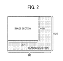
- one frame is formed of 845 columns x 525 rows, and 752 columns x 480 rows out of them are effective image sections. This complies with NTSC method.
- Fig. 3 is a whole functional block diagram of an embodiment of the exposure control unit 130 in Fig. 1 .
- the preprocessor 131 is formed of a conversion circuit 211 and a luminance adding circuit 212.
- An exposure control process function of the CPU 132 is formed of a difference arithmetic section 220, an optimum exposure amount arithmetic section 230, an exposure time/gain arithmetic section 240 and a controlling section 250.
- the optimum exposure amount arithmetic section 230 is formed of an optimum exposure amount variation arithmetic section 231, a corrected optimum exposure amount variation arithmetic section 232 and an optimum exposure amount calculating section 233.
- the exposure time/gain arithmetic section 240 is formed of a gain determining section 241 and an exposure time calculation section 242.
- the preprocessor 131 needs to process the image data continuously produced from the imaging element 102 one after another in synchronization with the vertical/horizontal synchronization signal, pixel clock, etc. Therefore, the conversion circuit 211 and the luminance adding circuit 212 of the preprocessor 131 are formed of hardware logic.
- the difference arithmetic section 220, the optimum exposure amount arithmetic section 230, the exposure time/gain arithmetic section 240 and the controlling section 250 work when the CPU 132 executes programs stored in the memory 133. In other words, cooperation of the CPU 132 and the programs make each of the sections work after the difference arithmetic section 220.
- the CPU 132 may combine process functions of the conversion circuit 211 and the luminance adding circuit 212 of the preprocessor 131.
- a hard logic may make process function of each of the sections work after the difference arithmetic section 220 work.
- the preprocessor 131 operates in synchronization with the vertical/horizontal synchronization signal, pixel clock, etc., but explanations of the vertical/horizontal synchronization signal, pixel clock, etc. are omitted unless necessary.
- the conversion circuit 211 of the preprocessor 131 sequentially receives image (pixel) data produced from the imaging element 102, and converts each of the data into luminance information Y and color-difference information CbCr.
- the conversion circuit 211 outputs the luminance information Y from the converted luminance information Y and color-difference information CbCr.
- the conversion circuit 211 converts the image data into the luminance information Y and the color-difference information CbCr, based on the following formulae.
- the luminance adding circuit 212 sequentially receives the luminance information Y of each of the image data produced from the conversion circuit 211, and adds the luminance information for one frame to calculate a luminance summation Y total per frame. Namely, Y total represents a luminance summation of the current frame.
- a range of calculating the luminance summation Y total in the frame may be designated from outside.
- the luminance summation Y total represents a luminance summation of all the pixels of 752 columns x 480 rows.
- all the areas of 752 columns x 480 rows are not always effective images.
- the upper and lower area or circumferential area are occasionally not effective images.
- the range of calculating the luminance summation Y total in the frame is designated by, e.g., a coordinate with X 1 to X i in a horizontal direction and Y 1 to Y j in a vertical direction.
- the luminance adding circuit 212 calculates Y total covering pixels included in the designated range for each frame.
- the range of calculating the luminance summation Y total in the frame may be designated by dividing the frame to plural cells and designating the cells.
- a specific example is shown in Fig. 4 .
- 752 columns x 480 rows of the frame in Fig. 2 is divided into 8 x 8 cells of 94 columns x 60 rows, and the shaded cells cover a range of calculating Y total .
- the blanking area is omitted.
- the luminance adding circuit 212 calculates Y total covering pixels included in the shaded cells in Fig. 4 for each frame.
- Te preprocessor 131 transmits an interrupt signal to the CPU 132 every time when calculating a luminance summation Y total of the current frame to send the luminance summation Y total to the CPU 132.
- the CPU 132 calculates an optimum exposure amount for the next frame, based on the luminance summation Y total of the current frame calculated by the preprocessor 131, and determines an optimum exposure time and a gain from the optimum exposure amount.
- Fig. 5 is a process flowchart of calculating an exposure time/gain executed in the CPU 132. An operation of each of the functions of the CPU 132 is explained according to Fig. 5 .
- the difference arithmetic section 220 receives the luminance summation Y total from the preprocessor 131 (STEP 1001) and calculates a difference error between a target value Y target and Y total (STEP 1002) by the following formula.
- the difference error (between the luminance summation of the current frame and the target value) calculated by the difference arithmetic section 220 is sent to the optimum exposure amount arithmetic section 230 and held by the memory 133.
- the memory 133 holds at least a difference between the luminance summation of the last frame and the target value (error 1) and the luminance summation of the last but one frame and the target value (error 2).
- the optimum exposure amount arithmetic section 230 calculates an optimum exposure amount of the optimum exposure amount variation arithmetic section 231, based on the error calculated by the difference arithmetic section 220 as follows.
- the PID control method is not necessarily used. PD control may be omitted.
- the corrected optimum exposure amount variation arithmetic section 232 calculates a corrected optimum exposure amount variation updata' from the optimum exposure amount variation updata calculated by the optimum exposure amount variation arithmetic section 231 (STEP 1004).
- the formula (4') prevents updata' from becoming too small because updata is too corrected when the current exposure amount is extremely low in the formula (4).
- the optimum exposure amount calculating section 233 calculates an optimum exposure amount exposure' of the following frame, using the corrected optimum exposure amount variation updata' calculated by the corrected optimum exposure amount variation arithmetic section 232 by the following formula (STEP 1005).
- exposure ⁇ exposure + updata ⁇
- the optimum exposure amount exposure' calculated by the optimum exposure amount arithmetic section 230 is sent to the exposure time/gain arithmetic section 240.
- the optimum exposure amount exposure' is held by the memory 133 and becomes the current exposure amount exposure by the following optimum exposure amount calculation.
- the exposure time/gain arithmetic section 240 calculates a gain and an exposure time of the imaging element 102, based on the optimum exposure amount exposure' calculated by the optimum exposure amount arithmetic section 230 as follows.
- the gain determining section 241 classifies the optimum exposure amount exposure' sent by the optimum exposure amount arithmetic section 230 into plural cases according to its size and determines a gain (STEP 1006).
- the optimum exposure amount exposure' is classified to 6 degrees of cases 0 to 5 according to its size as follows:
- the gain determining section 241 calculates an exposure amount the determined gain is removed from exposure withoutgain (STEP 1007).
- This exposure withoutgain is an exposure amount, the exposure time of which is calculated.
- exposure withoutgain exposure ⁇ - gain - 1 * exposure max In case 0, exposure min is exposure withoutgain . In case 5, exposure max is exposure withoutgain .
- gain is 1 and exposure' is exposure withoutgain .
- exposure min is exposure withoutgain to secure minimum exposure amount necessary.
- exposure max the gain is increased twice, triple or quadruple according to its size, and exposure max relevant to the gain is reduced from exposure' to determine exposure withoutgain .
- exposure max is exposure withoutgain to prevent the exposure amount from being too large.
- the gain is quadruple at maximum, but is typically N times, wherein N is an integer not less than 2.
- the gain determining section 241 sends the determined gain to the controlling section 250 and the exposure withoutgain the determined gain is removed from to the exposure time calculation section 242.
- the gain determining section 241 receives the exposure withoutgain , and calculates an exposure time as follows. (STEP 1008).
- rowexposure exposure withoutgain / N column
- pixelexposure exposure withoutgain - exposure withoutgain * N column
- [] is a round integer
- rowexposure is a row unit exposure time (exposure time row)
- pixelexposure is a pixel unit exposure time (exposure time line).
- the exposure time calculation section 242 sends the calculated exposure time to the controlling section 250.
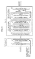
- Fig. 6 is a specific flowchart of the exposure time/gain arithmetic section 240 (detailed process flow of STEPS 1006 to 1008 in Fig. 5 ). The process flow in Fig. 6 repeats per frame.
- the gain determining section 241 of the exposure time/gain arithmetic section 240 receives the optimum exposure amount exposure' of the current frame from the optimum exposure amount arithmetic section 230 (STEP 2001) and determines which case (0 to 5) the exposure' is classified to (STEPS 202 to 2007). When classified to case 0, the gain is single (STEP 2008) and the predetermined exposure min is exposure withoutgain regardless of the exposure' (STEP 2009). When classified to case 1, 2, 3 or 4, the gain is single, double, triple or quadruple (STEPS 2010, 2011, 2012 and 2013), and exposure withoutgain is calculated using the formula (7) (STEP 2014).
- the gain is quadruple (STEP 2015) and exposure max is exposure withoutgain (STEP 2016).
- the exposure time calculation section 242 calculates an exposure time using the formula (8), based on exposure withoutgain (STEP 2017).
- the controlling section 250 receives the exposure time and the again sent from the exposure time/gain arithmetic section 240 and send them to the control circuit 102-3 of the imaging element 102 (STEP 1009). This is repeated per frame.
- Fig. 7 is a whole functional block diagram of another embodiment of the exposure control unit 130 in Fig. 1 .
- the preprocessor 131 uses a luminance histogram production circuit 214 in place of the luminance adding circuit 212 in Fig. 3 .
- the other configurations are same as those in Fig. 3 , the processes in the difference arithmetic section 220 and the optimum exposure amount variation arithmetic section 231 of the optimum exposure amount arithmetic section 230 are slightly different.
- the luminance histogram production circuit 214 of the preprocessor 131 sequentially receives luminance information Y of image (pixel) data produced from the conversion circuit 211 and counts the number of pixels of predetermined luminance level for one frame to produce a luminance histogram per frame.
- a significant image range may be designated from outside for a range of producing the histogram in a frame.
- Fig. 8 is a chart showing a specific configuration of the luminance histogram production circuit in 214.
- the luminance histogram production circuit in 214 has plural comparers (1) to (n) and plural counters (1) to (n). Each of the comparers and counters operates in synchronization with the vertical/horizontal synchronization signal, the pixel clock, but these signals are omitted in Fig. 8 .
- the luminance information Y produced from the conversion circuit 211 of the preprocessor 131 enters plural comparers (1) to (n). Thresholds are V1, V2...V(n-1) (V1 ⁇ V2... ⁇ V(n-1)).
- the comparer (1) makes the counter (1) +1 when Y ⁇ 1.
- the comparer (2) makes the counter (2) +1 when V1 ⁇ Y ⁇ V2.
- the comparer (n-1) makes the counter (n-1) +1 when V(n-2) ⁇ Y ⁇ V(n-1).
- the comparer (n) makes the counter (n) +1 when Y > V(n-1).
- the difference arithmetic section 220 receives the luminance histogram information from the luminance histogram production circuit in 214 and determines a summation of the number of bright luminance pixels N brightness and a summation of the number of dark luminance pixels of N darkness to calculate a difference error therebetween by the following formula.
- error N darkness - N brightness
- Drawing a line between bright luminance pixels and the dark luminance pixels may be determined from outside. In order to make an image brighter, the line is moved to the side of the bright luminance pixels. In order to make an image darker, the line is moved to the side of the dark luminance pixels.
- Fig. 9 is a chart for explaining drawing a line between bright pixels and dark pixels.
- the difference error (between a summation of the number of the bright luminance pixels and a summation of the number of the dark luminance pixels of the current frame) is sent to the optimum exposure amount arithmetic section 230 and held by the memory 113.
- the memory 113 holds at least a difference (error 1) between a summation of the number of the bright luminance pixels and a summation of the number of the dark luminance pixels of the last frame and a difference (error 2) between a summation of the number of the bright luminance pixels and a summation of the number of the dark luminance pixels of the last but one frame.
- Fig. 10 is a timing chart for explaining whole operations of the imaging apparatus.
- FV is a vertical effective period signal
- LV is a horizontal effective period signal, and are produced from the vertical and horizontal synchronization signals, respectively.
- PCLK is a pixel clock signal.
- the imaging element 102 produces image data for each frame during the FV signal period, and at the same time, performs exposure of the following image data.
- the exposure time includes a row unit exposure time (exposure time row) and a pixel unit exposure time (exposure time line).
- the maximum exposure time possible is one frame period (N column * N row scanning time).
- the image data A produced from the imaging element 102 is sent to the encoder 110 and the display 120, and taken in by the exposure control unit 130.
- the preprocessor 131 of the exposure control unit 130 sequentially adds the FV period of the frame 1 and luminance information of the image data A.
- the preprocessor 131 transmits an interrupt signal to the CPU 132 when the FV signal falls to send luminance summation information of the image data A to the CPU 132.
- the preprocessor 131 produces a FV period of the frame 1 and a luminance histogram of the image data A, and sends the luminance histogram information to the CPU 132 with an interrupt signal when the FV signal falls.
- the CPU 132 uses a vertical blanking period of the frame 1 to calculate an optimum exposure amount, based on the luminance summation information of the image data A or the luminance histogram information thereof, and determines an exposure time and a gain from the optimum exposure amount. The determined exposure time and gain are sent to the imaging element 102 and held thereby.
- the imaging element 102 produces image data B and parallely performs exposure of the following image data C.
- the exposure time of the image data C depends on the exposure time calculated from the image data A.
- the exposure control unit 130 determines the following exposure time and gain from the image data B as mentioned above.
- the imaging element 102 produces image data C and parallely performs exposure of the following image data D.
- the gain of the image data C depends on the gain calculated from the image data A
- the exposure time of the image data D depends on the exposure time calculated from the image data B.
- the imaging element 102 produces image data D and parallely performs exposure of the following image data E.
- the gain of the image data DC depends on the gain calculated from the image data B
- the exposure time of the image data E depends on the exposure time calculated from the image data C.
- the exposure time/gain are calculated in the vertical blanking period of each frame. However, the calculation of the exposure time/gain is thought to cross over to the following frame according to the imaging element and an operation speed of the CPU. In this case, image data the calculated exposure time/gain is applied to is delayed by one frame. When the exposure time/gain by the image data A is calculated across the frame, the exposure time/gain is reflected on the image data D of the frames 3 and 4.
Landscapes
- Engineering & Computer Science (AREA)
- Multimedia (AREA)
- Signal Processing (AREA)
- Physics & Mathematics (AREA)
- General Physics & Mathematics (AREA)
- Studio Devices (AREA)
Abstract
Description
- The present invention relates to an imaging apparatus, more particularly to exposure controlling technology of an imaging element thereof.
- An imaging apparatus uses an imaging element such as a CCD and a CMOS sensor. In the imaging apparatus, it is very important to control an exposure amount of the imaging element according to an object illuminance. When the exposure amount is not properly controlled according to the object illuminance, the object on an image is too white (exposure amount is so much that a pixel value is saturated) or too black (exposure amount is so little that a pixel value is close to zero).
- In order to properly adjust the exposure amount of the imaging element according to the object illuminance, an automatic exposure control method detecting a luminance level of an image signal produced by the imaging element and controlling an exposure time and a gain (analog gain or digital gain) such that the detected luminance level has a predetermined target value is conventionally known. In this case, the luminance level of an image signal produced by the imaging element is typically controlled to fall between the target value and a predetermined threshold. Namely, when the luminance level of an image signal falls between the target value and the predetermined threshold, the exposure amount is regarded as a proper exposure amount. This is because such a hysteresis prevents proper exposure control from oscillating. Further, an automatic exposure control method using PID (P: proportion, I: integration, D: differential) control is known as well. Even in this case, the coefficient is devised to prevent the oscillation.
- However, the conventional exposure control methods of the imaging element have a problem that a signal produced by the imaging element has a luminance level which is not accurately close to a target value. The problem is explained hereafter.
- When the exposure amount is small, e.g., the exposure time Ts = 1* Trow and this is status A. When the exposure amount is large, e.g., the exposure time T1 = 10 * Trow and this is status B. Trow is a time for the imaging element to scan a line in a horizontal direction.
- In the status A, when the exposure time is increased by a Trow, Ts is 2 * Trow which is twice as large as the original exposure amount. In the status B, when the exposure time is increased by a Trow, Ts is 11 * Trow which is 11/10 = 1.1 as large as the original exposure amount. Even when the exposure time is changed by the same rate, the exposure amount does not evenly change. Namely, in the conventional exposure control methods, a threshold is set regardless of the present exposure amount and only in consideration of a maximum light quantity variation, and the automatic exposure control deteriorates in accuracy when the exposure amount has a specific value or more.
- Japanese published unexamined application No.
10-336516
Because of these reasons, a need exist for an imaging element which does not quickly change in luminance in switching exposure amount (time) particularly when the exposure amount is small (exposure time is short). - Accordingly, one object of the present invention to provide an imaging element which does not quickly change in luminance in switching exposure amount (time) particularly when the exposure amount is small (exposure time is short) in its exposure control.
Another object of the present invention to provide a method of controlling exposure. - These objects and other objects of the present invention, either individually or collectively, have been satisfied by the discovery of an exposure controlling apparatus controlling an exposure amount of an imaging element, comprising:
- a first unit configured to determine an optimum exposure amount variation from an output luminance information of the imaging element;
- a second unit configured to determine a corrected optimum exposure amount variation by multiplying the optimum exposure amount variation with a value from dividing a current exposure amount with a maximum exposure amount obtainable by the imaging element;
- a third unit configured to determine an optimum exposure amount by adding the corrected optimum exposure amount variation to the current exposure amount;
- a fourth unit configured to determine an exposure time according to the optimum exposure amount; and
- a fifth unit configured to set the exposure time in the imaging element.
- These and other objects, features and advantages of the present invention will become apparent upon consideration of the following description of the preferred embodiments of the present invention taken in conjunction with the accompanying drawings.
- Various other objects, features and attendant advantages of the present invention will be more fully appreciated as the same becomes better understood from the detailed description when considered in connection with the accompanying drawings in which like reference characters designate like corresponding parts throughout and wherein:
-
Fig. 1 is a configuration diagram of an embodiment of the imaging apparatus of the present invention; -
Fig. 2 is a view illustrating a specific example of one frame; -
Fig. 3 is a functional block diagram of an embodiment of the exposure control unit inFig. 1 ; -
Fig. 4 is a chart for explaining a range of an image subjected to luminance summation calculation; -
Fig. 5 is a process flowchart of an embodiment of CPU of the exposure control unit; -
Fig. 6 is a detailed flowchart of the exposure time/gain arithmetic section inFig. 3 ; -
Fig. 7 is a functional block diagram of another embodiment of the exposure control unit inFig. 1 ; -
Fig. 8 is a chart showing a specific configuration of a luminance histogram production circuit inFig. 7 ; -
Fig. 9 is a chart for explaining drawing a line between bright pixels and dark pixels using the luminance histogram; and -
Fig. 10 is a timing chart for explaining whole operations of the imaging apparatus. - The present invention provides an imaging element which does not quickly change in luminance in switching exposure amount (time) particularly when the exposure amount is small (exposure time is short) in its exposure control.
More particularly, the present invention relates to an exposure controlling apparatus controlling an exposure amount of an imaging element, comprising: - a first unit configured to determine an optimum exposure amount variation from an output luminance information of the imaging element;
- a second unit configured to determine a corrected optimum exposure amount variation by multiplying the optimum exposure amount variation with a value from dividing a current exposure amount with a maximum exposure amount obtainable by the imaging element;
- a third unit configured to determine an optimum exposure amount by adding the corrected optimum exposure amount variation to the current exposure amount;
- a fourth unit configured to determine an exposure time according to the optimum exposure amount; and
- a fifth unit configured to set the exposure time in the imaging element.
-
Fig. 1 is a configuration diagram of an embodiment of the imaging apparatus of the present invention. The imaging apparatus includes animaging unit 100, anencoder 110, adisplay 120 and anexposure control unit 130 as an exposure controller. - The
imaging unit 100 includes anoptical system 101 and animaging element 102. Theoptical system 101 efficiently condense light from an object to theimaging element 102. Theimaging element 102 includes an optical sensor 102-1, a signal processing circuit 102-2 and a control circuit 102-3. The optical sensor 102-1 is a CDD sensor or a CMOS sensor, and converts an optical image of the object into an electrical signal (analog signal) according to its light intensity. The signal processing circuit 102-2 includes an AGC (Automatic Gain Controller) circuit adjusting an analog image signal produced from the optical sensor 102-1 to be a predetermined level, an A/D conversion circuit converting the image signal into a digital signal image data, a γ correction circuit executing a γ correction on the image data, and circuits executing other image processings. The AGC circuit is formed in a subsequent stage of the A/D conversion circuit and may adjust the digital signal image data to be a predetermined level. The control circuit 102-3 controls operations of the optical sensor 102-1 and the signal processing circuit 102-2. As mentioned later, the control circuit 102-3 receives exposure time and gain information from the exposure control unit per frame to adjust an exposure time (charge accumulation time) of the optical sensor 102-1 and a gain of the AGC circuit in the signal processing circuit 102-2. - The
imaging element 102 further includes a vertical/horizontal synchronization signal generation circuit, a pixel clock generation circuit and other timing signal generation circuits. - The
imaging element 102 continuously produces image (pixel) data in synchronization with the vertical/horizontal synchronization signal and the pixel clock. At th same time, theimaging element 102 produces the vertical/horizontal synchronization signal, pixel clock and other necessary timing signals. - The
encoder 110 sequentially receives image (pixel) data produced from theimaging element 102 together with the vertical/horizontal synchronization signal, pixel clock, etc., and converts the data into, e.g., an NTSC video signal (analog signal). The vertical/horizontal synchronization signal and other various signals are added to the video signal. Thedisplay 120 displays the video signal produced from theencoder 110, based on the vertical/horizontal synchronization signal and other signals. - The
exposure control unit 130 includes apreprocessor 131, aCPU 132 and amemory 133. Thepreprocessor 131 sequentially receives image (pixel) data produced from theimaging element 102 together with the vertical/horizontal synchronization signal, pixel clock, etc. and separates the image data into luminance information and a color-difference information, and adds the separated luminance information for one frame to calculate luminance summation per frame. TheCPU 132 receives the luminance information per frame calculated by thepreprocessor 131 and calculates an optimum exposure amount for the next frame and determines optimum exposure time and gain from the optimum exposure amount to make a luminance level of the image date produced from theimaging element 102 close to a predetermined target value. TheCPU 132 sends out the determined optimum exposure time and gain to the control circuit 102-3 of theimaging element 102. Thememory 133 includes volatile memories such as RAM and involatile memories such as ROM. Thememory 133 memorizes on-the-process data and processing result data in theCPU 132, and programs and parameters needed for the process of theCPU 132. - Hereafter, specific configuration and operation of the
exposure control unit 130 are explained in detail. AsFig. 2 shows, one frame is formed of 845 columns x 525 rows, and 752 columns x 480 rows out of them are effective image sections. This complies with NTSC method. -
Fig. 3 is a whole functional block diagram of an embodiment of theexposure control unit 130 inFig. 1 . InFig. 3 , thepreprocessor 131 is formed of aconversion circuit 211 and aluminance adding circuit 212. An exposure control process function of theCPU 132 is formed of a differencearithmetic section 220, an optimum exposure amountarithmetic section 230, an exposure time/gainarithmetic section 240 and a controllingsection 250. Further, the optimum exposure amountarithmetic section 230 is formed of an optimum exposure amount variationarithmetic section 231, a corrected optimum exposure amount variationarithmetic section 232 and an optimum exposureamount calculating section 233. The exposure time/gainarithmetic section 240 is formed of again determining section 241 and an exposuretime calculation section 242. - The
preprocessor 131 needs to process the image data continuously produced from theimaging element 102 one after another in synchronization with the vertical/horizontal synchronization signal, pixel clock, etc. Therefore, theconversion circuit 211 and theluminance adding circuit 212 of thepreprocessor 131 are formed of hardware logic. The differencearithmetic section 220, the optimum exposure amountarithmetic section 230, the exposure time/gainarithmetic section 240 and the controllingsection 250 work when theCPU 132 executes programs stored in thememory 133. In other words, cooperation of theCPU 132 and the programs make each of the sections work after the differencearithmetic section 220. - The
CPU 132 may combine process functions of theconversion circuit 211 and theluminance adding circuit 212 of thepreprocessor 131. A hard logic may make process function of each of the sections work after the differencearithmetic section 220 work. - First, operations of the
preprocessor 131 are explained. Thepreprocessor 131 operates in synchronization with the vertical/horizontal synchronization signal, pixel clock, etc., but explanations of the vertical/horizontal synchronization signal, pixel clock, etc. are omitted unless necessary. - The
conversion circuit 211 of thepreprocessor 131 sequentially receives image (pixel) data produced from theimaging element 102, and converts each of the data into luminance information Y and color-difference information CbCr. Theconversion circuit 211 outputs the luminance information Y from the converted luminance information Y and color-difference information CbCr. - When the image data is RGB color image data, the
conversion circuit 211 converts the image data into the luminance information Y and the color-difference information CbCr, based on the following formulae.


- The
luminance adding circuit 212 sequentially receives the luminance information Y of each of the image data produced from theconversion circuit 211, and adds the luminance information for one frame to calculate a luminance summation Ytotal per frame. Namely, Ytotal represents a luminance summation of the current frame. - In the
luminance adding circuit 212, a range of calculating the luminance summation Ytotal in the frame may be designated from outside.
When the frame has the configuration inFig. 2 , the luminance summation Ytotal represents a luminance summation of all the pixels of 752 columns x 480 rows. However, all the areas of 752 columns x 480 rows are not always effective images. The upper and lower area or circumferential area are occasionally not effective images. When the range of calculating the luminance summation Ytotal in the frame is designated from outside, an ineffective image area can be removed from calculation. - The range of calculating the luminance summation Ytotal in the frame is designated by, e.g., a coordinate with X1 to Xi in a horizontal direction and Y1 to Yj in a vertical direction. The
luminance adding circuit 212 calculates Ytotal covering pixels included in the designated range for each frame. - The range of calculating the luminance summation Ytotal in the frame may be designated by dividing the frame to plural cells and designating the cells. A specific example is shown in
Fig. 4 . 752 columns x 480 rows of the frame inFig. 2 is divided into 8 x 8 cells of 94 columns x 60 rows, and the shaded cells cover a range of calculating Ytotal. InFig. 4 , the blanking area is omitted. Theluminance adding circuit 212 calculates Ytotal covering pixels included in the shaded cells inFig. 4 for each frame. -
Te preprocessor 131 transmits an interrupt signal to theCPU 132 every time when calculating a luminance summation Ytotal of the current frame to send the luminance summation Ytotal to theCPU 132. TheCPU 132 calculates an optimum exposure amount for the next frame, based on the luminance summation Ytotal of the current frame calculated by thepreprocessor 131, and determines an optimum exposure time and a gain from the optimum exposure amount. -
Fig. 5 is a process flowchart of calculating an exposure time/gain executed in theCPU 132. An operation of each of the functions of theCPU 132 is explained according toFig. 5 . - The difference
arithmetic section 220 receives the luminance summation Ytotal from the preprocessor 131 (STEP 1001) and calculates a difference error between a target value Ytarget and Ytotal (STEP 1002) by the following formula.

wherein Bmax is a maximum pixel value (maximum brightness); Ncolum' is 752 and Nrow' is 480; and K' is typically about 0.2 and may be 0.4, 0.6, 0.8 and 1.0 according to the circumferential brightness. - The difference error (between the luminance summation of the current frame and the target value) calculated by the difference
arithmetic section 220 is sent to the optimum exposure amountarithmetic section 230 and held by thememory 133. Thememory 133 holds at least a difference between the luminance summation of the last frame and the target value (error 1) and the luminance summation of the last but one frame and the target value (error 2). - The optimum exposure amount
arithmetic section 230 calculates an optimum exposure amount of the optimum exposure amount variationarithmetic section 231, based on the error calculated by the differencearithmetic section 220 as follows. - First, the optimum exposure amount variation
arithmetic section 231 calculates an optimum exposure amount variation updata of the following frame with PID control method using theerror 1 and theerror 2 in addition to the error (STEP 1003) by the following formula:
- Next, the corrected optimum exposure amount variation
arithmetic section 232 calculates a corrected optimum exposure amount variation updata' from the optimum exposure amount variation updata calculated by the optimum exposure amount variation arithmetic section 231 (STEP 1004). Namely, updata is corrected by the following formula:
wherein exposure is a current exposure amount and exposuremax is a maximum exposure amount theimaging element 102 can have (when the exposure time is a maximum exposure time the optical sensor can have). exposuremax is determined by the following formula:
wherein Ncolum is 845 and Nrow is 525. - In the formula (4), when the exposure is small (exposure time is short), updata' is smaller than updata. When the exposure is large (exposure time is long), updata' is almost same as updata. Namely, when the exposure time is short, the exposure amount variation largely influences on the image luminance, but the formula (4) makes updata' small and the influence lessens.
- The formula (4) may be changed to the following formula (4') according to Ytarget.

Relations between the coefficient K and Ytarget are shows in Table 1. -
Table 1 Ytarge Coefficient K Bmax * Ncolum' * Nrow' * 0.2 10 Bmax * Ncolum' * Nrow' * 0.4 6 Bmax * Ncolum' * Nrow' * 0.6 4 Bmax * Ncolum' * Nrow' * 0.8 2 Bmax * Ncolum' * Nrow' * 1.0 1 - The formula (4') prevents updata' from becoming too small because updata is too corrected when the current exposure amount is extremely low in the formula (4).
- Next, the optimum exposure
amount calculating section 233 calculates an optimum exposure amount exposure' of the following frame, using the corrected optimum exposure amount variation updata' calculated by the corrected optimum exposure amount variationarithmetic section 232 by the following formula (STEP 1005).
- The optimum exposure amount exposure' calculated by the optimum exposure amount
arithmetic section 230 is sent to the exposure time/gainarithmetic section 240. The optimum exposure amount exposure' is held by thememory 133 and becomes the current exposure amount exposure by the following optimum exposure amount calculation. - The exposure time/gain
arithmetic section 240 calculates a gain and an exposure time of theimaging element 102, based on the optimum exposure amount exposure' calculated by the optimum exposure amountarithmetic section 230 as follows. - The
gain determining section 241 classifies the optimum exposure amount exposure' sent by the optimum exposure amountarithmetic section 230 into plural cases according to its size and determines a gain (STEP 1006). The optimum exposure amount exposure' is classified to 6 degrees ofcases 0 to 5 according to its size as follows: - Case 0: exposure' ≤ exposuremin
- gain single
- Case 1: exposuremin < exposure' ≤ exposuremax
- gain single
- Case 2: exposuremax < exposure' ≤ 2*exposuremax
- gain double
- Case 3: 2*exposuremax < exposure' ≤ 3*exposuremax
- gain triple
- Case 4: 3*exposuremax < exposure' ≤ 4*exposuremax
- gain quadruple
- Case 5: exposure' < 4*exposuremax
- gain quadruple
- Further, the
gain determining section 241 calculates an exposure amount the determined gain is removed from exposurewithoutgain (STEP 1007). This exposurewithoutgain is an exposure amount, the exposure time of which is calculated.
Incase 0, exposuremin is exposurewithoutgain. Incase 5, exposuremax is exposurewithoutgain. - Namely, while exposure' does not exceed exposuremax, gain is 1 and exposure' is exposurewithoutgain. When exposure' is less than exposuremin, exposuremin is exposurewithoutgain to secure minimum exposure amount necessary. When exposure' exceeds exposuremax, the gain is increased twice, triple or quadruple according to its size, and exposuremax relevant to the gain is reduced from exposure' to determine exposurewithoutgain. When exposure' exceeds 4*exposuremax, gain is quadruple at maximum, and exposuremax is exposurewithoutgain to prevent the exposure amount from being too large. The gain is quadruple at maximum, but is typically N times, wherein N is an integer not less than 2.
- The
gain determining section 241 sends the determined gain to the controllingsection 250 and the exposurewithoutgain the determined gain is removed from to the exposuretime calculation section 242. - The
gain determining section 241 receives the exposurewithoutgain, and calculates an exposure time as follows. (STEP 1008). -

wherein [] is a round integer, rowexposure is a row unit exposure time (exposure time row) and pixelexposure is a pixel unit exposure time (exposure time line). The exposuretime calculation section 242 sends the calculated exposure time to the controllingsection 250. -
Fig. 6 is a specific flowchart of the exposure time/gain arithmetic section 240 (detailed process flow ofSTEPS 1006 to 1008 inFig. 5 ). The process flow inFig. 6 repeats per frame. - The
gain determining section 241 of the exposure time/gainarithmetic section 240 receives the optimum exposure amount exposure' of the current frame from the optimum exposure amount arithmetic section 230 (STEP 2001) and determines which case (0 to 5) the exposure' is classified to (STEPS 202 to 2007). When classified tocase 0, the gain is single (STEP 2008) and the predetermined exposuremin is exposurewithoutgain regardless of the exposure' (STEP 2009). When classified tocase cases 0 to 4), the gain is quadruple (STEP 2015) and exposuremax is exposurewithoutgain (STEP 2016). The exposuretime calculation section 242 calculates an exposure time using the formula (8), based on exposurewithoutgain (STEP 2017). - Back to
Fig. 3 , the controllingsection 250 receives the exposure time and the again sent from the exposure time/gainarithmetic section 240 and send them to the control circuit 102-3 of the imaging element 102 (STEP 1009). This is repeated per frame. - Next, another embodiment of the present invention is explained. The whole configuration of the imaging apparatus is omitted because of being the same as that in
Fig. 1 . Thepreprocessor 131 in theexposure control unit 130 is different from that inFig. 1 . -
Fig. 7 is a whole functional block diagram of another embodiment of theexposure control unit 130 inFig. 1 . As is apparent from comparison betweenFigs. 7 and3 , thepreprocessor 131 uses a luminancehistogram production circuit 214 in place of theluminance adding circuit 212 inFig. 3 . The other configurations are same as those inFig. 3 , the processes in the differencearithmetic section 220 and the optimum exposure amount variationarithmetic section 231 of the optimum exposure amountarithmetic section 230 are slightly different. - Hereafter, the luminance
histogram production circuit 214, the differencearithmetic section 220 and the optimum exposure amount variationarithmetic section 231 inFig. 7 are explained.
The luminancehistogram production circuit 214 of thepreprocessor 131 sequentially receives luminance information Y of image (pixel) data produced from theconversion circuit 211 and counts the number of pixels of predetermined luminance level for one frame to produce a luminance histogram per frame. A significant image range may be designated from outside for a range of producing the histogram in a frame. -
Fig. 8 is a chart showing a specific configuration of the luminance histogram production circuit in 214. The luminance histogram production circuit in 214 has plural comparers (1) to (n) and plural counters (1) to (n). Each of the comparers and counters operates in synchronization with the vertical/horizontal synchronization signal, the pixel clock, but these signals are omitted inFig. 8 . - The luminance information Y produced from the
conversion circuit 211 of thepreprocessor 131 enters plural comparers (1) to (n). Thresholds are V1, V2...V(n-1) (V1 < V2...<V(n-1)). The comparer (1) makes the counter (1) +1 when Y ≤ 1. The comparer (2) makes the counter (2) +1 when V1 < Y ≤ V2. Similarly, the comparer (n-1) makes the counter (n-1) +1 when V(n-2) < Y ≤ V(n-1). The comparer (n) makes the counter (n) +1 when Y > V(n-1). These are repeated for one frame, and when one frame is finished, a counter value of each of the counters (1) to (n) is produced and the counters (1) to (n) are reset. The same operation is repeated for each frame. - Back to
Fig. 7 , the differencearithmetic section 220 receives the luminance histogram information from the luminance histogram production circuit in 214 and determines a summation of the number of bright luminance pixels Nbrightness and a summation of the number of dark luminance pixels of Ndarkness to calculate a difference error therebetween by the following formula.
Drawing a line between bright luminance pixels and the dark luminance pixels may be determined from outside. In order to make an image brighter, the line is moved to the side of the bright luminance pixels. In order to make an image darker, the line is moved to the side of the dark luminance pixels.Fig. 9 is a chart for explaining drawing a line between bright pixels and dark pixels. - The difference error (between a summation of the number of the bright luminance pixels and a summation of the number of the dark luminance pixels of the current frame) is sent to the optimum exposure amount
arithmetic section 230 and held by the memory 113. The memory 113 holds at least a difference (error 1) between a summation of the number of the bright luminance pixels and a summation of the number of the dark luminance pixels of the last frame and a difference (error 2) between a summation of the number of the bright luminance pixels and a summation of the number of the dark luminance pixels of the last but one frame. - The optimum exposure amount variation
arithmetic section 231 of the differencearithmetic section 220 calculates an optimum exposure amount variation updata of the following frame with PID control method using theerror 1 and theerror 2 in addition to the error of the current frame by the following formula:
wherein Kp', Ki' and Kd' are PID control coefficients and empirically determined. These include normalized coefficients as well. - The other operations of the difference
arithmetic section 220, and operations of the exposure time/gainarithmetic section 240 and the controllingsection 250 have been already explained and explanations thereof are omitted. -
Fig. 10 is a timing chart for explaining whole operations of the imaging apparatus. InFig. 10 , FV is a vertical effective period signal and LV is a horizontal effective period signal, and are produced from the vertical and horizontal synchronization signals, respectively. PCLK is a pixel clock signal. - The
imaging element 102 produces image data for each frame during the FV signal period, and at the same time, performs exposure of the following image data. The exposure time includes a row unit exposure time (exposure time row) and a pixel unit exposure time (exposure time line). The maximum exposure time possible is one frame period (Ncolumn * Nrow scanning time). - Now, assuming that the
imaging element 102 is producing image data A, and at the same time, performing exposure of the following image data B. - The image data A produced from the
imaging element 102 is sent to theencoder 110 and thedisplay 120, and taken in by theexposure control unit 130. Thepreprocessor 131 of theexposure control unit 130 sequentially adds the FV period of theframe 1 and luminance information of the image data A. Thepreprocessor 131 transmits an interrupt signal to theCPU 132 when the FV signal falls to send luminance summation information of the image data A to theCPU 132. InFig. 7 , thepreprocessor 131 produces a FV period of theframe 1 and a luminance histogram of the image data A, and sends the luminance histogram information to theCPU 132 with an interrupt signal when the FV signal falls. - The
CPU 132 uses a vertical blanking period of theframe 1 to calculate an optimum exposure amount, based on the luminance summation information of the image data A or the luminance histogram information thereof, and determines an exposure time and a gain from the optimum exposure amount. The determined exposure time and gain are sent to theimaging element 102 and held thereby. - In the
following frame 2, theimaging element 102 produces image data B and parallely performs exposure of the following image data C. The exposure time of the image data C depends on the exposure time calculated from the image data A. Further, in theframe 2, theexposure control unit 130 determines the following exposure time and gain from the image data B as mentioned above. - In the
following frame 3, theimaging element 102 produces image data C and parallely performs exposure of the following image data D. The gain of the image data C depends on the gain calculated from the image data A, and the exposure time of the image data D depends on the exposure time calculated from the image data B. - Similarly, in the
following frame 4, theimaging element 102 produces image data D and parallely performs exposure of the following image data E. The gain of the image data DC depends on the gain calculated from the image data B, and the exposure time of the image data E depends on the exposure time calculated from the image data C. - In
Fig. 10 , the exposure time/gain are calculated in the vertical blanking period of each frame. However, the calculation of the exposure time/gain is thought to cross over to the following frame according to the imaging element and an operation speed of the CPU. In this case, image data the calculated exposure time/gain is applied to is delayed by one frame. When the exposure time/gain by the image data A is calculated across the frame, the exposure time/gain is reflected on the image data D of theframes
Claims (11)
- An exposure controlling apparatus controlling an exposure amount of an imaging element, comprising:a first unit configured to determine an optimum exposure amount variation from an output luminance information of the imaging element;a second unit configured to determine a corrected optimum exposure amount variation by multiplying the optimum exposure amount variation with a value from dividing a current exposure amount with a maximum exposure amount obtainable by the imaging element;a third unit configured to determine an optimum exposure amount by adding the corrected optimum exposure amount variation to the current exposure amount;a fourth unit configured to determine an exposure time according to the optimum exposure amount; anda fifth unit configured to set the exposure time in the imaging element.
- The exposure controlling apparatus of Claim 1, further comprising:a sixth unit configured to add the luminance information for one frame to calculate a luminance summation per frame,wherein the first unit determines the optimum exposure amount variation from a difference between the luminance summation and a predetermined target value per frame.
- The exposure controlling apparatus of Claim 2, wherein the optimum exposure amount variation is determined by the following formula:

wherein updata represents the optimum exposure amount variation; error represents a difference between a luminance summation of the current frame and a target value; error 1 represents a difference between a luminance summation of the last frame and a target value; error 2 represents a difference between a luminance summation of the last frame but one and a target value; and Kp, Ki and Kd are coefficients. - The exposure controlling apparatus of Claim 1, further comprising:a seventh unit configured to produce a luminance histogram per frame on output luminance information of the imaging element,wherein the first unit determines the optimum exposure amount variation from a difference between a summation of the number of bright luminance pixels and a summation of the number of dark luminance pixels obtained from the luminance histogram per frame.
- The exposure controlling apparatus of Claim 4, wherein the optimum exposure amount variation is determined by the following formula:

wherein updata represents the optimum exposure amount variation; error represents a difference between a summation of the number of the bright luminance pixels and a summation of the number of the dark luminance pixels of the current frame; error 1 represents a difference between a summation of the number of the bright luminance pixels and a summation of the number of the dark luminance pixels of the last frame; error 2 represents a difference between a summation of the number of the bright luminance pixels and a summation of the number of the dark luminance pixels of the last frame but one; and Kp', Ki' and Kd' are coefficients. - The exposure controlling apparatus of any one of Claims 1 to 5, wherein the second unit determines the corrected optimum exposure amount variation by further multiplying the optimum exposure amount variation with a predetermined coefficient.
- The exposure controlling apparatus of any one of Claims 1 to 6, further comprising:an eighth unit configured to determine a gain of the imaging element when the optimum exposure amount exceeds the maximum exposure amount obtainable by the imaging element such that the gain increases according to the exceeded exposure amount and to determine an exposure amount by removing the increase of the gain from the optimum exposure amount,wherein the fourth unit determines an exposure time according to the exposure amount the increase of the gain is removed from, andthe fifth unit sets the exposure time according to the exposure amount the increase of the gain is removed from and the determined gain in the imaging element.
- The exposure controlling apparatus of Claim 7, wherein the eighth unit sets the gain as 1 when the optimum exposure amount is not greater than a minimum exposure amount needed by the imaging element, and the exposure amount as the minimum exposure amount; and
sets the gain as N which is an integer not less than 2 when the optimum exposure amount is greater than N times of the maximum exposure amount, and the exposure amount as the exposure maximum amount. - A method of controlling an exposure amount of an imaging element, comprising:determining an optimum exposure amount variation from an output luminance information of the imaging element;determining a corrected optimum exposure amount variation by multiplying the optimum exposure amount variation with a value from dividing a current exposure amount with a maximum exposure amount obtainable by the imaging element;determining an optimum exposure amount by adding the corrected optimum exposure amount variation to the current exposure amount;determining an exposure time according to the optimum exposure amount; andsetting the exposure time in the imaging element.
- The method of Claim 9, further comprising:determining a gain of the imaging element when the optimum exposure amount exceeds the maximum exposure amount obtainable by the imaging element such that the gain increases according to the exceeded exposure amount and to determine an exposure amount by removing the increase of the gain from the optimum exposure amount,wherein the step of determining an exposure time according to the optimum exposure amount comprises determining the exposure time according to the exposure amount the increase of the gain is removed from, andthe step of setting the exposure time in the imaging element comprises setting the exposure time according to the exposure amount the increase of the gain is removed from and the determined gain in the imaging element.
- An image forming apparatus, comprising:an optical system configured to form an optical image of an object;an imaging element configured to image the optical image; andthe exposure controlling apparatus of any one of Claims 1 to 8.
Applications Claiming Priority (2)
| Application Number | Priority Date | Filing Date | Title |
|---|---|---|---|
| JP2011200690 | 2011-09-14 | ||
| JP2012164711A JP5978829B2 (en) | 2011-09-14 | 2012-07-25 | Image sensor exposure control apparatus and method, and image pickup apparatus |
Publications (2)
| Publication Number | Publication Date |
|---|---|
| EP2571256A1 true EP2571256A1 (en) | 2013-03-20 |
| EP2571256B1 EP2571256B1 (en) | 2018-10-24 |
Family
ID=47044759
Family Applications (1)
| Application Number | Title | Priority Date | Filing Date |
|---|---|---|---|
| EP12181571.6A Not-in-force EP2571256B1 (en) | 2011-09-14 | 2012-08-23 | Exposure controlling apparatus and method of imaging element, and imaging apparatus |
Country Status (2)
| Country | Link |
|---|---|
| EP (1) | EP2571256B1 (en) |
| JP (1) | JP5978829B2 (en) |
Cited By (2)
| Publication number | Priority date | Publication date | Assignee | Title |
|---|---|---|---|---|
| CN106471797A (en) * | 2014-07-10 | 2017-03-01 | 英特尔公司 | For accelerating the platform architecture of camera control algorithm |
| US12307736B2 (en) | 2021-09-03 | 2025-05-20 | Lasertec Corporation | Image processing apparatus and image processing method |
Families Citing this family (1)
| Publication number | Priority date | Publication date | Assignee | Title |
|---|---|---|---|---|
| JP2019041392A (en) * | 2018-10-01 | 2019-03-14 | ルネサスエレクトロニクス株式会社 | Imaging device and control method of lens module |
Citations (4)
| Publication number | Priority date | Publication date | Assignee | Title |
|---|---|---|---|---|
| JPH10336516A (en) | 1997-05-28 | 1998-12-18 | Toshiba Corp | Video camera with automatic sensitivity switching device |
| US20060044459A1 (en) * | 2004-08-31 | 2006-03-02 | Casio Computer Co., Ltd. | Image pickup apparatus, exposure control method, and computer program installed in the image pickup apparatus |
| US20090073287A1 (en) * | 2007-09-18 | 2009-03-19 | Olympus Corporation | Image capturing device |
| US20100066858A1 (en) * | 2008-09-12 | 2010-03-18 | Sony Corporation | Imaging apparatus and imaging mode control method |
Family Cites Families (2)
| Publication number | Priority date | Publication date | Assignee | Title |
|---|---|---|---|---|
| JP2801256B2 (en) * | 1989-04-07 | 1998-09-21 | キヤノン株式会社 | Exposure control device |
| JP2002218320A (en) * | 2001-01-22 | 2002-08-02 | Sharp Corp | Imaging device and control method thereof |
-
2012
- 2012-07-25 JP JP2012164711A patent/JP5978829B2/en not_active Expired - Fee Related
- 2012-08-23 EP EP12181571.6A patent/EP2571256B1/en not_active Not-in-force
Patent Citations (4)
| Publication number | Priority date | Publication date | Assignee | Title |
|---|---|---|---|---|
| JPH10336516A (en) | 1997-05-28 | 1998-12-18 | Toshiba Corp | Video camera with automatic sensitivity switching device |
| US20060044459A1 (en) * | 2004-08-31 | 2006-03-02 | Casio Computer Co., Ltd. | Image pickup apparatus, exposure control method, and computer program installed in the image pickup apparatus |
| US20090073287A1 (en) * | 2007-09-18 | 2009-03-19 | Olympus Corporation | Image capturing device |
| US20100066858A1 (en) * | 2008-09-12 | 2010-03-18 | Sony Corporation | Imaging apparatus and imaging mode control method |
Cited By (3)
| Publication number | Priority date | Publication date | Assignee | Title |
|---|---|---|---|---|
| CN106471797A (en) * | 2014-07-10 | 2017-03-01 | 英特尔公司 | For accelerating the platform architecture of camera control algorithm |
| EP3167606A4 (en) * | 2014-07-10 | 2018-03-07 | Intel Corporation | Platform architecture for accelerated camera control algorithms |
| US12307736B2 (en) | 2021-09-03 | 2025-05-20 | Lasertec Corporation | Image processing apparatus and image processing method |
Also Published As
| Publication number | Publication date |
|---|---|
| EP2571256B1 (en) | 2018-10-24 |
| JP5978829B2 (en) | 2016-08-24 |
| JP2013078108A (en) | 2013-04-25 |
Similar Documents
| Publication | Publication Date | Title |
|---|---|---|
| US9654697B2 (en) | Solid-state imaging apparatus and driving method of solid-state imaging apparatus | |
| US8149302B2 (en) | Method of processing noise in image data, noise reduction unit, and imaging apparatus | |
| US20100328498A1 (en) | Shooting parameter adjustment method for face detection and image capturing device for face detection | |
| US9253374B2 (en) | Image processing apparatus and method for controlling the same for obtaining and applying gamma characteristics to reduce a difference between light and dark areas of an image | |
| US8368804B2 (en) | Imaging control apparatus, imaging control method, and computer-readable storage medium | |
| US20100045798A1 (en) | Electronic camera | |
| US20160219229A1 (en) | Image capturing apparatus and control method thereof | |
| US20070159537A1 (en) | Imaging apparatus and method | |
| US10412356B2 (en) | Image processing apparatus and image processing method | |
| US20120162467A1 (en) | Image capture device | |
| US20150222800A1 (en) | Imaging Apparatus | |
| US10027919B2 (en) | Signal processing apparatus, image capturing apparatus, control apparatus, signal processing method, and control method | |
| US20220239819A1 (en) | Device, control method, and storage medium | |
| US7999863B2 (en) | Image correction apparatus and method | |
| US8502893B2 (en) | Imaging apparatus, flash determination method, and recording medium | |
| US20140362282A1 (en) | Exposure controller | |
| US20150222829A1 (en) | Imaging apparatus | |
| KR101795604B1 (en) | Auto focuse adjusting apparatus and controlling method thereof | |
| EP2571256B1 (en) | Exposure controlling apparatus and method of imaging element, and imaging apparatus | |
| US20050179789A1 (en) | Color image processing method, and color imaging apparatus | |
| JP2009124638A (en) | Image signal processing circuit | |
| JP2008005081A (en) | Authentication device | |
| JP2007228200A (en) | Brightness correction apparatus for moving picture, control method thereof and control program thereof | |
| US10594912B2 (en) | Flash band determination device for detecting flash band, method of controlling the same, storage medium, and image pickup apparatus | |
| US20140240495A1 (en) | Surveillance device and control method of the same |
Legal Events
| Date | Code | Title | Description |
|---|---|---|---|
| PUAI | Public reference made under article 153(3) epc to a published international application that has entered the european phase |
Free format text: ORIGINAL CODE: 0009012 |
|
| 17P | Request for examination filed |
Effective date: 20120823 |
|
| AK | Designated contracting states |
Kind code of ref document: A1 Designated state(s): AL AT BE BG CH CY CZ DE DK EE ES FI FR GB GR HR HU IE IS IT LI LT LU LV MC MK MT NL NO PL PT RO RS SE SI SK SM TR |
|
| AX | Request for extension of the european patent |
Extension state: BA ME |
|
| 17Q | First examination report despatched |
Effective date: 20150319 |
|
| STAA | Information on the status of an ep patent application or granted ep patent |
Free format text: STATUS: EXAMINATION IS IN PROGRESS |
|
| GRAP | Despatch of communication of intention to grant a patent |
Free format text: ORIGINAL CODE: EPIDOSNIGR1 |
|
| STAA | Information on the status of an ep patent application or granted ep patent |
Free format text: STATUS: GRANT OF PATENT IS INTENDED |
|
| INTG | Intention to grant announced |
Effective date: 20180710 |
|
| GRAS | Grant fee paid |
Free format text: ORIGINAL CODE: EPIDOSNIGR3 |
|
| GRAA | (expected) grant |
Free format text: ORIGINAL CODE: 0009210 |
|
| STAA | Information on the status of an ep patent application or granted ep patent |
Free format text: STATUS: THE PATENT HAS BEEN GRANTED |
|
| AK | Designated contracting states |
Kind code of ref document: B1 Designated state(s): AL AT BE BG CH CY CZ DE DK EE ES FI FR GB GR HR HU IE IS IT LI LT LU LV MC MK MT NL NO PL PT RO RS SE SI SK SM TR |
|
| REG | Reference to a national code |
Ref country code: GB Ref legal event code: FG4D |
|
| REG | Reference to a national code |
Ref country code: CH Ref legal event code: EP |
|
| REG | Reference to a national code |
Ref country code: IE Ref legal event code: FG4D |
|
| REG | Reference to a national code |
Ref country code: AT Ref legal event code: REF Ref document number: 1058059 Country of ref document: AT Kind code of ref document: T Effective date: 20181115 |
|
| REG | Reference to a national code |
Ref country code: DE Ref legal event code: R096 Ref document number: 602012052512 Country of ref document: DE |
|
| REG | Reference to a national code |
Ref country code: NL Ref legal event code: MP Effective date: 20181024 |
|
| REG | Reference to a national code |
Ref country code: LT Ref legal event code: MG4D |
|
| REG | Reference to a national code |
Ref country code: AT Ref legal event code: MK05 Ref document number: 1058059 Country of ref document: AT Kind code of ref document: T Effective date: 20181024 |
|
| PG25 | Lapsed in a contracting state [announced via postgrant information from national office to epo] |
Ref country code: NL Free format text: LAPSE BECAUSE OF FAILURE TO SUBMIT A TRANSLATION OF THE DESCRIPTION OR TO PAY THE FEE WITHIN THE PRESCRIBED TIME-LIMIT Effective date: 20181024 |
|
| PG25 | Lapsed in a contracting state [announced via postgrant information from national office to epo] |
Ref country code: FI Free format text: LAPSE BECAUSE OF FAILURE TO SUBMIT A TRANSLATION OF THE DESCRIPTION OR TO PAY THE FEE WITHIN THE PRESCRIBED TIME-LIMIT Effective date: 20181024 Ref country code: IS Free format text: LAPSE BECAUSE OF FAILURE TO SUBMIT A TRANSLATION OF THE DESCRIPTION OR TO PAY THE FEE WITHIN THE PRESCRIBED TIME-LIMIT Effective date: 20190224 Ref country code: BG Free format text: LAPSE BECAUSE OF FAILURE TO SUBMIT A TRANSLATION OF THE DESCRIPTION OR TO PAY THE FEE WITHIN THE PRESCRIBED TIME-LIMIT Effective date: 20190124 Ref country code: PL Free format text: LAPSE BECAUSE OF FAILURE TO SUBMIT A TRANSLATION OF THE DESCRIPTION OR TO PAY THE FEE WITHIN THE PRESCRIBED TIME-LIMIT Effective date: 20181024 Ref country code: LT Free format text: LAPSE BECAUSE OF FAILURE TO SUBMIT A TRANSLATION OF THE DESCRIPTION OR TO PAY THE FEE WITHIN THE PRESCRIBED TIME-LIMIT Effective date: 20181024 Ref country code: NO Free format text: LAPSE BECAUSE OF FAILURE TO SUBMIT A TRANSLATION OF THE DESCRIPTION OR TO PAY THE FEE WITHIN THE PRESCRIBED TIME-LIMIT Effective date: 20190124 Ref country code: ES Free format text: LAPSE BECAUSE OF FAILURE TO SUBMIT A TRANSLATION OF THE DESCRIPTION OR TO PAY THE FEE WITHIN THE PRESCRIBED TIME-LIMIT Effective date: 20181024 Ref country code: LV Free format text: LAPSE BECAUSE OF FAILURE TO SUBMIT A TRANSLATION OF THE DESCRIPTION OR TO PAY THE FEE WITHIN THE PRESCRIBED TIME-LIMIT Effective date: 20181024 Ref country code: AT Free format text: LAPSE BECAUSE OF FAILURE TO SUBMIT A TRANSLATION OF THE DESCRIPTION OR TO PAY THE FEE WITHIN THE PRESCRIBED TIME-LIMIT Effective date: 20181024 Ref country code: HR Free format text: LAPSE BECAUSE OF FAILURE TO SUBMIT A TRANSLATION OF THE DESCRIPTION OR TO PAY THE FEE WITHIN THE PRESCRIBED TIME-LIMIT Effective date: 20181024 |
|
| PG25 | Lapsed in a contracting state [announced via postgrant information from national office to epo] |
Ref country code: AL Free format text: LAPSE BECAUSE OF FAILURE TO SUBMIT A TRANSLATION OF THE DESCRIPTION OR TO PAY THE FEE WITHIN THE PRESCRIBED TIME-LIMIT Effective date: 20181024 Ref country code: SE Free format text: LAPSE BECAUSE OF FAILURE TO SUBMIT A TRANSLATION OF THE DESCRIPTION OR TO PAY THE FEE WITHIN THE PRESCRIBED TIME-LIMIT Effective date: 20181024 Ref country code: GR Free format text: LAPSE BECAUSE OF FAILURE TO SUBMIT A TRANSLATION OF THE DESCRIPTION OR TO PAY THE FEE WITHIN THE PRESCRIBED TIME-LIMIT Effective date: 20190125 Ref country code: RS Free format text: LAPSE BECAUSE OF FAILURE TO SUBMIT A TRANSLATION OF THE DESCRIPTION OR TO PAY THE FEE WITHIN THE PRESCRIBED TIME-LIMIT Effective date: 20181024 Ref country code: PT Free format text: LAPSE BECAUSE OF FAILURE TO SUBMIT A TRANSLATION OF THE DESCRIPTION OR TO PAY THE FEE WITHIN THE PRESCRIBED TIME-LIMIT Effective date: 20190224 |
|
| REG | Reference to a national code |
Ref country code: DE Ref legal event code: R097 Ref document number: 602012052512 Country of ref document: DE |
|
| PG25 | Lapsed in a contracting state [announced via postgrant information from national office to epo] |
Ref country code: IT Free format text: LAPSE BECAUSE OF FAILURE TO SUBMIT A TRANSLATION OF THE DESCRIPTION OR TO PAY THE FEE WITHIN THE PRESCRIBED TIME-LIMIT Effective date: 20181024 Ref country code: DK Free format text: LAPSE BECAUSE OF FAILURE TO SUBMIT A TRANSLATION OF THE DESCRIPTION OR TO PAY THE FEE WITHIN THE PRESCRIBED TIME-LIMIT Effective date: 20181024 Ref country code: CZ Free format text: LAPSE BECAUSE OF FAILURE TO SUBMIT A TRANSLATION OF THE DESCRIPTION OR TO PAY THE FEE WITHIN THE PRESCRIBED TIME-LIMIT Effective date: 20181024 |
|
| PG25 | Lapsed in a contracting state [announced via postgrant information from national office to epo] |
Ref country code: EE Free format text: LAPSE BECAUSE OF FAILURE TO SUBMIT A TRANSLATION OF THE DESCRIPTION OR TO PAY THE FEE WITHIN THE PRESCRIBED TIME-LIMIT Effective date: 20181024 Ref country code: RO Free format text: LAPSE BECAUSE OF FAILURE TO SUBMIT A TRANSLATION OF THE DESCRIPTION OR TO PAY THE FEE WITHIN THE PRESCRIBED TIME-LIMIT Effective date: 20181024 Ref country code: SK Free format text: LAPSE BECAUSE OF FAILURE TO SUBMIT A TRANSLATION OF THE DESCRIPTION OR TO PAY THE FEE WITHIN THE PRESCRIBED TIME-LIMIT Effective date: 20181024 Ref country code: SM Free format text: LAPSE BECAUSE OF FAILURE TO SUBMIT A TRANSLATION OF THE DESCRIPTION OR TO PAY THE FEE WITHIN THE PRESCRIBED TIME-LIMIT Effective date: 20181024 |
|
| PLBE | No opposition filed within time limit |
Free format text: ORIGINAL CODE: 0009261 |
|
| STAA | Information on the status of an ep patent application or granted ep patent |
Free format text: STATUS: NO OPPOSITION FILED WITHIN TIME LIMIT |
|
| 26N | No opposition filed |
Effective date: 20190725 |
|
| PG25 | Lapsed in a contracting state [announced via postgrant information from national office to epo] |
Ref country code: SI Free format text: LAPSE BECAUSE OF FAILURE TO SUBMIT A TRANSLATION OF THE DESCRIPTION OR TO PAY THE FEE WITHIN THE PRESCRIBED TIME-LIMIT Effective date: 20181024 |
|
| PG25 | Lapsed in a contracting state [announced via postgrant information from national office to epo] |
Ref country code: TR Free format text: LAPSE BECAUSE OF FAILURE TO SUBMIT A TRANSLATION OF THE DESCRIPTION OR TO PAY THE FEE WITHIN THE PRESCRIBED TIME-LIMIT Effective date: 20181024 |
|
| PG25 | Lapsed in a contracting state [announced via postgrant information from national office to epo] |
Ref country code: LU Free format text: LAPSE BECAUSE OF NON-PAYMENT OF DUE FEES Effective date: 20190823 Ref country code: LI Free format text: LAPSE BECAUSE OF NON-PAYMENT OF DUE FEES Effective date: 20190831 Ref country code: MC Free format text: LAPSE BECAUSE OF FAILURE TO SUBMIT A TRANSLATION OF THE DESCRIPTION OR TO PAY THE FEE WITHIN THE PRESCRIBED TIME-LIMIT Effective date: 20181024 Ref country code: CH Free format text: LAPSE BECAUSE OF NON-PAYMENT OF DUE FEES Effective date: 20190831 |
|
| REG | Reference to a national code |
Ref country code: BE Ref legal event code: MM Effective date: 20190831 |
|
| PG25 | Lapsed in a contracting state [announced via postgrant information from national office to epo] |
Ref country code: IE Free format text: LAPSE BECAUSE OF NON-PAYMENT OF DUE FEES Effective date: 20190823 |
|
| PG25 | Lapsed in a contracting state [announced via postgrant information from national office to epo] |
Ref country code: BE Free format text: LAPSE BECAUSE OF NON-PAYMENT OF DUE FEES Effective date: 20190831 |
|
| PG25 | Lapsed in a contracting state [announced via postgrant information from national office to epo] |
Ref country code: CY Free format text: LAPSE BECAUSE OF FAILURE TO SUBMIT A TRANSLATION OF THE DESCRIPTION OR TO PAY THE FEE WITHIN THE PRESCRIBED TIME-LIMIT Effective date: 20181024 |
|
| PG25 | Lapsed in a contracting state [announced via postgrant information from national office to epo] |
Ref country code: HU Free format text: LAPSE BECAUSE OF FAILURE TO SUBMIT A TRANSLATION OF THE DESCRIPTION OR TO PAY THE FEE WITHIN THE PRESCRIBED TIME-LIMIT; INVALID AB INITIO Effective date: 20120823 Ref country code: MT Free format text: LAPSE BECAUSE OF FAILURE TO SUBMIT A TRANSLATION OF THE DESCRIPTION OR TO PAY THE FEE WITHIN THE PRESCRIBED TIME-LIMIT Effective date: 20181024 |
|
| PGFP | Annual fee paid to national office [announced via postgrant information from national office to epo] |
Ref country code: FR Payment date: 20210819 Year of fee payment: 10 |
|
| PGFP | Annual fee paid to national office [announced via postgrant information from national office to epo] |
Ref country code: DE Payment date: 20210819 Year of fee payment: 10 Ref country code: GB Payment date: 20210820 Year of fee payment: 10 |
|
| PG25 | Lapsed in a contracting state [announced via postgrant information from national office to epo] |
Ref country code: MK Free format text: LAPSE BECAUSE OF FAILURE TO SUBMIT A TRANSLATION OF THE DESCRIPTION OR TO PAY THE FEE WITHIN THE PRESCRIBED TIME-LIMIT Effective date: 20181024 |
|
| REG | Reference to a national code |
Ref country code: DE Ref legal event code: R119 Ref document number: 602012052512 Country of ref document: DE |
|
| GBPC | Gb: european patent ceased through non-payment of renewal fee |
Effective date: 20220823 |
|
| PG25 | Lapsed in a contracting state [announced via postgrant information from national office to epo] |
Ref country code: FR Free format text: LAPSE BECAUSE OF NON-PAYMENT OF DUE FEES Effective date: 20220831 Ref country code: DE Free format text: LAPSE BECAUSE OF NON-PAYMENT OF DUE FEES Effective date: 20230301 |
|
| PG25 | Lapsed in a contracting state [announced via postgrant information from national office to epo] |
Ref country code: GB Free format text: LAPSE BECAUSE OF NON-PAYMENT OF DUE FEES Effective date: 20220823 |