EP2570900A1 - Electronic device and method for scanning a touch panel thereof - Google Patents
Electronic device and method for scanning a touch panel thereof Download PDFInfo
- Publication number
- EP2570900A1 EP2570900A1 EP12006471A EP12006471A EP2570900A1 EP 2570900 A1 EP2570900 A1 EP 2570900A1 EP 12006471 A EP12006471 A EP 12006471A EP 12006471 A EP12006471 A EP 12006471A EP 2570900 A1 EP2570900 A1 EP 2570900A1
- Authority
- EP
- European Patent Office
- Prior art keywords
- preset
- touch
- charge
- touch sensors
- touch sensor
- Prior art date
- Legal status (The legal status is an assumption and is not a legal conclusion. Google has not performed a legal analysis and makes no representation as to the accuracy of the status listed.)
- Ceased
Links
Images







Classifications
-
- G—PHYSICS
- G06—COMPUTING OR CALCULATING; COUNTING
- G06F—ELECTRIC DIGITAL DATA PROCESSING
- G06F3/00—Input arrangements for transferring data to be processed into a form capable of being handled by the computer; Output arrangements for transferring data from processing unit to output unit, e.g. interface arrangements
- G06F3/01—Input arrangements or combined input and output arrangements for interaction between user and computer
- G06F3/03—Arrangements for converting the position or the displacement of a member into a coded form
- G06F3/041—Digitisers, e.g. for touch screens or touch pads, characterised by the transducing means
- G06F3/044—Digitisers, e.g. for touch screens or touch pads, characterised by the transducing means by capacitive means
-
- G—PHYSICS
- G06—COMPUTING OR CALCULATING; COUNTING
- G06F—ELECTRIC DIGITAL DATA PROCESSING
- G06F3/00—Input arrangements for transferring data to be processed into a form capable of being handled by the computer; Output arrangements for transferring data from processing unit to output unit, e.g. interface arrangements
- G06F3/01—Input arrangements or combined input and output arrangements for interaction between user and computer
- G06F3/03—Arrangements for converting the position or the displacement of a member into a coded form
- G06F3/041—Digitisers, e.g. for touch screens or touch pads, characterised by the transducing means
- G06F3/0416—Control or interface arrangements specially adapted for digitisers
- G06F3/0418—Control or interface arrangements specially adapted for digitisers for error correction or compensation, e.g. based on parallax, calibration or alignment
- G06F3/04184—Synchronisation with the driving of the display or the backlighting unit to avoid interferences generated internally
-
- G—PHYSICS
- G06—COMPUTING OR CALCULATING; COUNTING
- G06F—ELECTRIC DIGITAL DATA PROCESSING
- G06F3/00—Input arrangements for transferring data to be processed into a form capable of being handled by the computer; Output arrangements for transferring data from processing unit to output unit, e.g. interface arrangements
- G06F3/01—Input arrangements or combined input and output arrangements for interaction between user and computer
- G06F3/03—Arrangements for converting the position or the displacement of a member into a coded form
- G06F3/041—Digitisers, e.g. for touch screens or touch pads, characterised by the transducing means
- G06F3/0416—Control or interface arrangements specially adapted for digitisers
- G06F3/0418—Control or interface arrangements specially adapted for digitisers for error correction or compensation, e.g. based on parallax, calibration or alignment
-
- G—PHYSICS
- G06—COMPUTING OR CALCULATING; COUNTING
- G06F—ELECTRIC DIGITAL DATA PROCESSING
- G06F3/00—Input arrangements for transferring data to be processed into a form capable of being handled by the computer; Output arrangements for transferring data from processing unit to output unit, e.g. interface arrangements
- G06F3/01—Input arrangements or combined input and output arrangements for interaction between user and computer
- G06F3/03—Arrangements for converting the position or the displacement of a member into a coded form
- G06F3/041—Digitisers, e.g. for touch screens or touch pads, characterised by the transducing means
- G06F3/044—Digitisers, e.g. for touch screens or touch pads, characterised by the transducing means by capacitive means
- G06F3/0446—Digitisers, e.g. for touch screens or touch pads, characterised by the transducing means by capacitive means using a grid-like structure of electrodes in at least two directions, e.g. using row and column electrodes
Definitions
- the present invention relates to an electronic device and a method for scanning a touch panel thereof. More particularly, the present invention relates to charging the touch sensors of the touch panel in the aforementioned scanning.
- Fig. 1 is a schematic diagram showing a conventional electronic device 100 including a touch controller 120 and a touch panel 140, which is a capacitive touch panel.
- the touch panel 140 includes a set of driving lines (the vertical lines) and a set of sensing lines (the horizontal lines). Each location where a driving line crosses a sensing line is a touch sensor of the touch panel 140. For example, three touch sensors of the touch panel 140 are marked as 142, 144 and 146, respectively.
- the touch controller 120 can detect resultant touch events by scanning the touch panel 140. For scanning of the touch panel 140, the touch controller 120 sends driving signals to the driving lines of the touch panel 140. The driving signals charges the touch sensors of the touch panel 140 and the touch sensors generate sensing signals in response. Next, the touch controller 120 receives the sensing signals from the sensing lines of the touch panel 140. The touch controller 120 analyzes the sensing signals to determine the locations of the touch events.
- the electronic device 100 may perform predetermined functions according to the touch events.
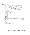
- FIG. 2 is a schematic diagram showing the curves 202, 204 and 206 of the voltage-time characteristics of the charging of the touch sensors 142, 144 and 146 of the conventional touch panel 140, respectively.
- a far-end touch sensor such as the touch sensor 146 charges slower than a near-end touch sensor such as the touch sensor 142 charges because the far-end touch sensor has a larger time constant.
- the time constant of a touch sensor is the product of the equivalent resistance and the equivalent capacitance of the touch sensor.
- the near-end touch sensor 142 takes a period T N to charge to the voltage level V R
- the far-end touch sensor 146 takes a much longer period T F to charge to the voltage level V R .
- the touch sensors of a conventional touch panel are all charged according to the same charge period, which might cause undercharge or overcharge of the touch sensors.
- the touch sensors 144 and 146 are undercharged when all the touch sensors are charged according to the charge period T N
- the touch sensors 142 and 144 are overcharged when all the touch sensors are charged according to the charge period T F .
- the present invention is directed to an electronic device and a method for scanning a touch panel of the electronic device.
- the electronic device and the method can solve or alleviate the aforementioned noise problem and charge problem.
- an electronic device includes a touch panel and a control circuitry.
- the touch panel includes a plurality of touch sensors.
- the control circuitry is coupled to the touch panel.
- the control circuitry charges each of the touch sensors according to a preset charge period of the touch sensor and detects the maximum difference in charge characteristics of the touch sensors.
- the control circuitry adjusts the preset charge periods of the touch sensors according to the charge characteristics of the touch sensors and a preset limit of the preset charge periods of the touch sensors when the maximum difference is higher than a preset threshold.
- an electronic device includes a display and a control circuitry.
- the display is integrated with a plurality of touch sensors.
- the display may be liquid crystal display, OLED (organic light emitting) display, in-cell, on-cell display or transparent OLED display.
- the control circuitry is coupled to the touch panel.
- the control circuitry charges each of the touch sensors according to a preset charge period of the touch sensor and detects the maximum difference in charge characteristics of the touch sensors.
- the control circuitry adjusts the preset charge periods of the touch sensors according to the charge characteristics of the touch sensors and a preset limit of the preset charge periods of the touch sensors when the maximum difference is higher than a preset threshold.
- a method for scanning a touch panel of the aforementioned electronic device includes the following steps. Charge each touch sensor of the touch panel according to the preset charge period of each touch sensor. Detect the maximum difference in charge characteristics of the touch sensors of the touch panel. Adjust the preset charge periods of the touch sensors according to the charge characteristics of the touch sensors and a preset limit of the preset charge periods of the touch sensors when the maximum difference is higher than a preset threshold.
- Fig. 1 is a schematic diagram showing a conventional electronic device with a touch panel.
- Fig. 2 is a schematic diagram showing the charging of the touch sensors of a conventional touch panel.
- Fig. 3 is a schematic diagram showing an electronic device according to an embodiment of the present invention.
- Fig. 4 is a flow chart showing a method for charging a touch panel of an electronic device according to an embodiment of the present invention.
- Fig. 5 is a schematic diagram showing the charging of the touch sensors of a touch panel according to an embodiment of the present invention.
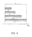
- Fig. 6 is a schematic diagram showing the preset charge periods of the touch sensors of a touch panel according to an embodiment of the present invention.
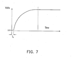
- Fig. 7 is a schematic diagram showing the preset charge delay of a touch sensor of a touch panel according to an embodiment of the present invention.
- Fig. 8 is a schematic diagram showing the preset charge periods and the preset charge delays of the touch sensors of a touch panel according to an embodiment of the present invention.
- Figs. 9-12 are schematic diagrams showing electronic devices according to some embodiments of the present invention.
- Fig. 3 is a schematic diagram showing an electronic device 300 according to an embodiment of the present invention.
- the electronic device 300 may be a smart phone, a personal digital assistant, a tablet computer or a notebook computer.
- the electronic device 300 includes a touch panel 340 and a control circuitry 320 coupled to the touch panel 340.
- the touch panel 340 may be a capacitive touch panel that includes a plurality of touch sensors for sensing touch events, such as the touch sensors 342, 344 and 346.
- the control circuitry 320 may detect touch events by scanning the touch panel 340.
- the control circuitry 320 scans the touch panel 340 by sending driving signals to the touch panel 340 to charge the touch sensors and then receiving and analyzing the sensing signals from the touch panel 340.
- the electronic device 300 may execute predetermined functions according to the touch events.
- Fig. 4 is a flow chart showing a method for charging a touch panel of an electronic device according to an embodiment of the present invention.
- the method may be executed by the control circuitry 320 on the touch panel 340.
- the method may also be executed by another similar control circuitry on another similar touch panel.
- step 410 charge some or all of the touch sensors of the touch panel.
- Each touch sensor is charged according to a preset charge period of the touch sensor.
- the present charge period is the length of time for which a touch sensor is charged.
- the preset charge period of each touch sensor is the same default value.
- the preset charge period of each touch sensor may be a value which was determined when the method in Fig. 4 was executed previously and the preset charge periods of the touch sensors may be the same or different.
- step 420 detect charge characteristics of the touch sensors and detect the maximum difference in charge characteristics of the touch sensors.
- the charge characteristic of each touch sensor may be the voltage level to which the touch sensor is charged in the preset charge period of the touch sensor.
- the charge characteristic of each touch sensor may be the time constant of the touch sensor.
- step 430 compare the maximum difference in the charge characteristics of the touch sensors with a preset threshold.
- the flow proceeds to step 450.
- the control circuitry keeps the preset charge periods of the touch sensors unchanged and the control circuitry charge each touch sensor according to the preset charge period of the touch sensor. Since the maximum difference in the charge characteristics of the touch sensors is lower than the preset threshold, the conventional problem of non-uniform charge does not exist in this case.
- step 440 adjusts the preset charge periods of the touch sensors according to the charge characteristics of the touch sensors and a preset limit T L of the preset charge periods of the touch sensors.
- a purpose of the adjustment in step 440 is determining the preset charge period of each touch sensor to unify the voltage level to which each touch sensor is charged in order to avoid the conventional problem of non-uniform charge.
- Another purpose of the adjustment in step 440 is limiting the lengths of the preset charge periods of the touch sensors in order to avoid the interference of noises.
- the preset charge periods determined in step 440 may be stored in a table to be used later.
- step 450 the control circuitry charges each touch sensor according to the preset charge period of the touch sensor determined in step 440.
- the control circuitry first determines the length of the preset charge period of the slowest touch sensor with the largest time constant among the touch sensors according to the preset limit T L .
- the control circuitry sets the length of the preset charge period of the slowest touch sensor to be the time the slowest touch sensor takes to be fully charged to the ideal voltage level V I when the slowest touch sensor can be fully charged to V I in the preset limit T L .
- the control circuitry sets the length of the preset charge period of the slowest touch sensor to be the preset limit T L when the slowest touch sensor cannot be fully charged in the preset limit T L .
- the ideal voltage level V I is the voltage level to which each touch sensor should be charged for the scanning of the touch panel. A partially charged touch sensor can still detect touch events as long as the voltage level to which the touch sensor is charged is not too much lower than the ideal voltage level V I .
- Fig. 5 is a schematic diagram showing the charging of three touch sensors of a touch panel according to an embodiment of the present invention.
- the curves 501-503 show the voltage-time characteristics of the charging of the three touch sensors, respectively.
- the slowest touch sensor with the largest time constant is corresponding to the curve 503.
- the control circuitry may set the length of the preset charge period of each of the other touch sensors to be the time the touch sensor takes to be charged to the same voltage level V L .
- the slowest touch sensor takes a period of time T S to charge to the voltage level V L .
- the other two touch sensors take the periods of time T 1 and T 2 to charge to the voltage level V L , respectively. Therefore, the control circuitry sets the lengths of the preset charge periods of the other two touch sensors to be T 1 and T 2 , respectively.
- the control circuitry may detect the voltage level V L by charging the slowest touch sensor or calculate the voltage level V L according to the charge characteristic of the slowest touch sensor.
- the control circuitry may detect the lengths of T 1 and T 2 by charging the other two touch sensors or calculate the lengths of T 1 and T 2 according to the voltage level V L and the charge characteristics of the other two touch sensors.
- Fig. 6 is a schematic diagram showing the preset charge periods of four touch sensors of a touch panel according to an embodiment of the present invention.
- T L is the preset limit of the preset charge periods of the touch sensors.
- T P1 , T P2 , T P3 and T P4 are the preset charge periods of the four touch sensors determined by the control circuitry in step 440 in the aforementioned manner, respectively.
- the touch sensors begin charging at the same moment and end charging at different moments. The charging of the fastest touch sensor with the smallest time constant ends first.
- the preset charge periods T P1 , T P2 , T P3 and T P4 of the touch sensors span no longer than the preset limit T L .
- the control circuitry may determine not only the preset charge periods of the touch sensors but also the preset charge delays of the touch sensors.
- Fig. 7 is a schematic diagram showing the preset charge delay of a touch sensor of a touch panel according to an embodiment of the present invention.
- T D is the preset charge delay of the touch sensor. As shown in Fig. 7 , the touch sensor does not charge until its preset charge delay T D expires.
- the control circuitry charges each of the touch sensors according to the preset charge period and the preset charge delay of the touch sensor.
- the control circuitry keeps the preset charge periods and the preset charge delays of the touch sensors unchanged.
- the control circuitry adjusts the preset charge periods and the preset charge delays of the touch sensors according to the charge characteristics of the touch sensors and the preset limit T L in step 440.
- Fig. 8 is a schematic diagram showing the preset charge periods and the preset charge delays of four touch sensors of a touch panel according to an embodiment of the present invention.
- T L is the preset limit of the preset charge periods of the touch sensors.
- T P1 , T P2 , T P3 and T P4 are the preset charge periods of the four touch sensors determined by the control circuitry in step 440 in the aforementioned manner, respectively.
- T D1 , T D2 and T D3 are the preset charge delays of three of the four touch sensors determined by the control circuitry in step 440, respectively.
- the preset charge delay of the slowest touch sensor with the largest time constant is zero. As shown in Fig.
- the touch sensors begin charging at different moments and end charging at the same moment.
- the charging of the fastest touch sensor with the smallest time constant begins last.
- the preset charge periods T P1 , T P2 , T P3 and T P4 of the touch sensors span no longer than the preset limit T L .
- the example in Fig. 6 may be considered as a special case of the example in Fig. 8 in which the preset charge delays are all zero.
- the control circuitry may arrange the preset charge delays of the touch sensors arbitrarily as long as the preset charge periods of the touch sensors span no longer than the preset limit T L .
- Fig. 9 is a schematic diagram showing an electronic device 900 according to an embodiment of the present invention.
- the electronic device 900 includes a touch panel 940 and a control circuitry 920.
- the control circuitry 920 includes a touch driver 925.
- the touch driver 925 may execute the method for scanning a touch panel discussed above on the touch panel 940.
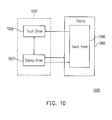
- Fig. 10 is a schematic diagram showing an electronic device 1000 according to another embodiment of the present invention.
- the electronic device 1000 includes a touch panel 1040, an display 1060 and a control circuitry 1020.
- the touch panel 1040 includes a plurality of touch sensors.
- the touch panel 1040 is integrated as a part of the display 1060.
- the conductive layers of the touch panel 1040 may be fabricated among the layers of the display 1060.
- the control circuitry 1020 includes a touch driver 1025 and a display driver 1027.
- the display driver 1027 drives the pixels of the display 1060 to display images, such as the graphical user interfaces of the electronic device 1000.
- the touch driver 1025 and the display driver 1027 cooperate to execute the method for scanning a touch panel discussed above on the touch panel 1040.
- the display driver 1027 executes steps 410 and 450.
- the display driver 1027 sends driving signals to the touch panel 1040 to charge the touch sensors and the touch driver 1025 receives the resultant sensing signals from the touch panel 1040.
- the touch driver 1025 may decide when to charge the touch sensors and send a control signal to inform the display driver 1027 to begin sending the driving signals to the touch sensors.
- the display driver 1027 may decide when to charge the touch sensors and send a control signal to inform the touch driver 1025 to receive the sensing signals from the touch sensors.
- the touch driver 1025 executes step 420.
- the touch driver 1025 or the display driver 1027 may execute step 430.
- the touch driver 1025 or the display driver 1027 may execute step 440 to determine the preset charge periods (or both the preset charge periods and the preset charge delays) of the touch sensors of the touch panel 1040.
- the touch driver 1025 sends a control signal to inform the display driver 1027 of the preset charge periods (or both the preset charge periods and the preset charge delays) of the touch sensors.
- the touch driver 1025 sends a control signal to inform the display driver 1027 of the necessary data, such as the charge characteristics of the touch sensors.
- Fig. 11 is a schematic diagram showing an electronic device 1100 according to another embodiment of the present invention.
- the electronic device 1100 includes a touch panel 1140 and a control circuitry 1120.
- the control circuitry 1120 includes a process unit 1123 and a touch driver 1125.
- the process unit 1123 is the main system of the electronic device 1100.
- the process unit 1123 and the touch driver 1125 cooperate to execute the method for scanning a touch panel discussed above on the touch panel 1140.
- the process unit 1123 executes predetermined functions of the electronic device 1100 according to the detected touch events.
- the touch driver 1125 executes steps 410, 420 and 450.
- the process unit 1123 executes step 440 to determine the preset charge periods (or both the preset charge periods and the preset charge delays) of the touch sensors of the touch panel 1140.
- the process unit 1123 or the touch driver 1125 executes step 430.
- Fig. 12 is a schematic diagram showing an electronic device 1200 according to another embodiment of the present invention.
- the electronic device 1200 includes a touch panel 1240, an display 1260 and a control circuitry 1220.
- the touch panel 1240 is integrated as a part of the display 1260.
- the control circuitry 1220 includes a system 1223, a touch driver 1225 and a display driver 1227.
- the system 1223 is the main system of the electronic device 1200.
- the display driver 1227 drives the pixels of the display 1260 to display images, such as the graphical user interfaces of the electronic device 1200.
- the system 1223, the touch driver 1225 and the display driver 1227 cooperate to execute the method for scanning a touch panel discussed above on the touch panel 1240.
- the system 1223 executes predetermined functions of the electronic device 1200 according to the detected touch events.
- the display driver 1227 executes steps 410 and 450.
- the display driver 1227 sends driving signals to the touch panel 1240 to charge the touch sensors and the touch driver 1225 receives the resultant sensing signals from the touch panel 1240.
- the touch driver 1225 or the display driver 1227 may decide when to charge the touch sensors.
- the touch driver 1225 executes step 420.
- the system 1223, the touch driver 1225 or the display driver 1227 may execute step 430.
- the system 1223 executes step 440 to determine the preset charge periods (or both the preset charge periods and the preset charge delays) of the touch sensors of the touch panel 1240.
- the present invention sets difference charge periods (or different charge periods and different charge delays) for the touch sensors of a touch panel in order to prevent the conventional problem of non-uniform charge of the touch sensors.
- the present invention imposes a preset limit on the preset charge periods of the touch sensors in order to avoid or alleviate the interference of noises during the scanning of a touch panel.
Landscapes
- Engineering & Computer Science (AREA)
- General Engineering & Computer Science (AREA)
- Theoretical Computer Science (AREA)
- Human Computer Interaction (AREA)
- Physics & Mathematics (AREA)
- General Physics & Mathematics (AREA)
- Position Input By Displaying (AREA)
Abstract
Description
- This application claims the priority benefits of
U.S. provisional application serial no. 61/535,377, filed on September 16, 2011 - The present invention relates to an electronic device and a method for scanning a touch panel thereof. More particularly, the present invention relates to charging the touch sensors of the touch panel in the aforementioned scanning.
-
Fig. 1 is a schematic diagram showing a conventionalelectronic device 100 including atouch controller 120 and atouch panel 140, which is a capacitive touch panel. Thetouch panel 140 includes a set of driving lines (the vertical lines) and a set of sensing lines (the horizontal lines). Each location where a driving line crosses a sensing line is a touch sensor of thetouch panel 140. For example, three touch sensors of thetouch panel 140 are marked as 142, 144 and 146, respectively. - When a user performs some operations on the
touch panel 140, thetouch controller 120 can detect resultant touch events by scanning thetouch panel 140. For scanning of thetouch panel 140, thetouch controller 120 sends driving signals to the driving lines of thetouch panel 140. The driving signals charges the touch sensors of thetouch panel 140 and the touch sensors generate sensing signals in response. Next, thetouch controller 120 receives the sensing signals from the sensing lines of thetouch panel 140. Thetouch controller 120 analyzes the sensing signals to determine the locations of the touch events. Theelectronic device 100 may perform predetermined functions according to the touch events. - In the scanning of a touch panel, noises often affect the sensing signals and cause erroneous results of the detection of touch events. The noise is always a problem. For example, many electronic devices, such as smart phones and tablet computers, are equipped with touch displays that consist of touch panels and liquid crystal modules (LCMs). An LCM generates a lot of noises when the polarities of its pixels are inverted.
- Another conventional problem is the different charge times of the touch sensors of a touch panel. The equivalent resistances and equivalent capacitances of the touch sensors of a touch panel are not uniform, which means the charge characteristics of the touch sensors are not uniform, either.
Fig. 2 is a schematic diagram showing thecurves touch sensors conventional touch panel 140, respectively. As shown inFig. 2 , a far-end touch sensor such as thetouch sensor 146 charges slower than a near-end touch sensor such as thetouch sensor 142 charges because the far-end touch sensor has a larger time constant. Here the time constant of a touch sensor is the product of the equivalent resistance and the equivalent capacitance of the touch sensor. Ideally, in the scanning of thetouch panel 140, all touch sensors are required to charge to the voltage level VR. The near-end touch sensor 142 takes a period TN to charge to the voltage level VR, while the far-end touch sensor 146 takes a much longer period TF to charge to the voltage level VR. - However, the touch sensors of a conventional touch panel are all charged according to the same charge period, which might cause undercharge or overcharge of the touch sensors. For example, the
touch sensors touch sensors - Accordingly, the present invention is directed to an electronic device and a method for scanning a touch panel of the electronic device. The electronic device and the method can solve or alleviate the aforementioned noise problem and charge problem.
- According to an embodiment of the present invention, an electronic device is provided. The electronic device includes a touch panel and a control circuitry. The touch panel includes a plurality of touch sensors. The control circuitry is coupled to the touch panel. The control circuitry charges each of the touch sensors according to a preset charge period of the touch sensor and detects the maximum difference in charge characteristics of the touch sensors. The control circuitry adjusts the preset charge periods of the touch sensors according to the charge characteristics of the touch sensors and a preset limit of the preset charge periods of the touch sensors when the maximum difference is higher than a preset threshold.
- According to another embodiment of the present invention, an electronic device is provided. The electronic device includes a display and a control circuitry. The display is integrated with a plurality of touch sensors. The display may be liquid crystal display, OLED (organic light emitting) display, in-cell, on-cell display or transparent OLED display. The control circuitry is coupled to the touch panel. The control circuitry charges each of the touch sensors according to a preset charge period of the touch sensor and detects the maximum difference in charge characteristics of the touch sensors. The control circuitry adjusts the preset charge periods of the touch sensors according to the charge characteristics of the touch sensors and a preset limit of the preset charge periods of the touch sensors when the maximum difference is higher than a preset threshold.
- According to another embodiment of the present invention, a method for scanning a touch panel of the aforementioned electronic device is provided. The method includes the following steps. Charge each touch sensor of the touch panel according to the preset charge period of each touch sensor. Detect the maximum difference in charge characteristics of the touch sensors of the touch panel. Adjust the preset charge periods of the touch sensors according to the charge characteristics of the touch sensors and a preset limit of the preset charge periods of the touch sensors when the maximum difference is higher than a preset threshold.
- The accompanying drawings are included to provide a further understanding of the invention, and are incorporated in and constitute a part of this specification. The drawings illustrate embodiments of the invention and, together with the description, serve to explain the principles of the invention.
-
Fig. 1 is a schematic diagram showing a conventional electronic device with a touch panel. -
Fig. 2 is a schematic diagram showing the charging of the touch sensors of a conventional touch panel. -
Fig. 3 is a schematic diagram showing an electronic device according to an embodiment of the present invention. -
Fig. 4 is a flow chart showing a method for charging a touch panel of an electronic device according to an embodiment of the present invention. -
Fig. 5 is a schematic diagram showing the charging of the touch sensors of a touch panel according to an embodiment of the present invention. -
Fig. 6 is a schematic diagram showing the preset charge periods of the touch sensors of a touch panel according to an embodiment of the present invention. -
Fig. 7 is a schematic diagram showing the preset charge delay of a touch sensor of a touch panel according to an embodiment of the present invention. -
Fig. 8 is a schematic diagram showing the preset charge periods and the preset charge delays of the touch sensors of a touch panel according to an embodiment of the present invention. -
Figs. 9-12 are schematic diagrams showing electronic devices according to some embodiments of the present invention. - Reference will now be made in detail to the present embodiments of the invention, examples of which are illustrated in the accompanying drawings. Wherever possible, the same reference numbers are used in the drawings and the description to refer to the same or like parts.
-
Fig. 3 is a schematic diagram showing anelectronic device 300 according to an embodiment of the present invention. Theelectronic device 300 may be a smart phone, a personal digital assistant, a tablet computer or a notebook computer. Theelectronic device 300 includes atouch panel 340 and acontrol circuitry 320 coupled to thetouch panel 340. Thetouch panel 340 may be a capacitive touch panel that includes a plurality of touch sensors for sensing touch events, such as thetouch sensors control circuitry 320 may detect touch events by scanning thetouch panel 340. Thecontrol circuitry 320 scans thetouch panel 340 by sending driving signals to thetouch panel 340 to charge the touch sensors and then receiving and analyzing the sensing signals from thetouch panel 340. Theelectronic device 300 may execute predetermined functions according to the touch events. -
Fig. 4 is a flow chart showing a method for charging a touch panel of an electronic device according to an embodiment of the present invention. The method may be executed by thecontrol circuitry 320 on thetouch panel 340. The method may also be executed by another similar control circuitry on another similar touch panel. - The flow shown in
Fig. 4 is discussed below. Instep 410, charge some or all of the touch sensors of the touch panel. Each touch sensor is charged according to a preset charge period of the touch sensor. Here the present charge period is the length of time for which a touch sensor is charged. Whenstep 410 is executed for the first time, the preset charge period of each touch sensor is the same default value. Whenstep 410 is executed later, the preset charge period of each touch sensor may be a value which was determined when the method inFig. 4 was executed previously and the preset charge periods of the touch sensors may be the same or different. - In
step 420, detect charge characteristics of the touch sensors and detect the maximum difference in charge characteristics of the touch sensors. In this embodiment, the charge characteristic of each touch sensor may be the voltage level to which the touch sensor is charged in the preset charge period of the touch sensor. Alternatively, the charge characteristic of each touch sensor may be the time constant of the touch sensor. Instep 430, compare the maximum difference in the charge characteristics of the touch sensors with a preset threshold. - When the maximum difference is lower than the preset threshold, the flow proceeds to step 450. The control circuitry keeps the preset charge periods of the touch sensors unchanged and the control circuitry charge each touch sensor according to the preset charge period of the touch sensor. Since the maximum difference in the charge characteristics of the touch sensors is lower than the preset threshold, the conventional problem of non-uniform charge does not exist in this case.
- When the maximum difference in the charge characteristics of the touch sensors is higher than or equal to the preset threshold, the flow proceeds to step 440 to adjust the preset charge periods of the touch sensors according to the charge characteristics of the touch sensors and a preset limit TL of the preset charge periods of the touch sensors. A purpose of the adjustment in
step 440 is determining the preset charge period of each touch sensor to unify the voltage level to which each touch sensor is charged in order to avoid the conventional problem of non-uniform charge. Another purpose of the adjustment instep 440 is limiting the lengths of the preset charge periods of the touch sensors in order to avoid the interference of noises. The preset charge periods determined instep 440 may be stored in a table to be used later. Next, instep 450, the control circuitry charges each touch sensor according to the preset charge period of the touch sensor determined instep 440. - The longer the charge period of a touch sensor, the more noises might appear during the charge period. Therefore, there is a preset limit TL of the preset charge periods of the touch sensors in this embodiment. The preset charge period of each touch sensor must be shorter than or equal to the preset limit TL. In
step 440, the control circuitry first determines the length of the preset charge period of the slowest touch sensor with the largest time constant among the touch sensors according to the preset limit TL. The control circuitry sets the length of the preset charge period of the slowest touch sensor to be the time the slowest touch sensor takes to be fully charged to the ideal voltage level VI when the slowest touch sensor can be fully charged to VI in the preset limit TL. Alternatively, the control circuitry sets the length of the preset charge period of the slowest touch sensor to be the preset limit TL when the slowest touch sensor cannot be fully charged in the preset limit TL. The ideal voltage level VI is the voltage level to which each touch sensor should be charged for the scanning of the touch panel. A partially charged touch sensor can still detect touch events as long as the voltage level to which the touch sensor is charged is not too much lower than the ideal voltage level VI. - Next, the control circuitry determines the lengths of the preset charge periods of the other touch sensors according to the length of the preset charge period of the slowest touch sensor and the charge characteristics of the other touch sensors. For example, please refer to
Fig. 5. Fig. 5 is a schematic diagram showing the charging of three touch sensors of a touch panel according to an embodiment of the present invention. The curves 501-503 show the voltage-time characteristics of the charging of the three touch sensors, respectively. The slowest touch sensor with the largest time constant is corresponding to thecurve 503. - Assume the slowest touch sensor is charged to the voltage level VL in its preset charge period determined according to the preset limit TL in the aforementioned manner. VL may be lower than or equal to the ideal voltage level VI. The control circuitry may set the length of the preset charge period of each of the other touch sensors to be the time the touch sensor takes to be charged to the same voltage level VL. As shown in
Fig. 5 , the slowest touch sensor takes a period of time TS to charge to the voltage level VL. The other two touch sensors take the periods of time T1 and T2 to charge to the voltage level VL, respectively. Therefore, the control circuitry sets the lengths of the preset charge periods of the other two touch sensors to be T1 and T2, respectively. The control circuitry may detect the voltage level VL by charging the slowest touch sensor or calculate the voltage level VL according to the charge characteristic of the slowest touch sensor. The control circuitry may detect the lengths of T1 and T2 by charging the other two touch sensors or calculate the lengths of T1 and T2 according to the voltage level VL and the charge characteristics of the other two touch sensors. -
Fig. 6 is a schematic diagram showing the preset charge periods of four touch sensors of a touch panel according to an embodiment of the present invention. InFig. 6 , TL is the preset limit of the preset charge periods of the touch sensors. TP1, TP2, TP3 and TP4 are the preset charge periods of the four touch sensors determined by the control circuitry instep 440 in the aforementioned manner, respectively. As shown inFig. 6 , the touch sensors begin charging at the same moment and end charging at different moments. The charging of the fastest touch sensor with the smallest time constant ends first. The preset charge periods TP1, TP2, TP3 and TP4 of the touch sensors span no longer than the preset limit TL. - In some other embodiments of the present invention, the control circuitry may determine not only the preset charge periods of the touch sensors but also the preset charge delays of the touch sensors.
Fig. 7 is a schematic diagram showing the preset charge delay of a touch sensor of a touch panel according to an embodiment of the present invention. TD is the preset charge delay of the touch sensor. As shown inFig. 7 , the touch sensor does not charge until its preset charge delay TD expires. - When the preset charge delays are involved, the method shown in
Fig. 4 needs the following modification. Insteps step 430, the control circuitry keeps the preset charge periods and the preset charge delays of the touch sensors unchanged. When the maximum difference is higher than or equal to the preset threshold instep 430, the control circuitry adjusts the preset charge periods and the preset charge delays of the touch sensors according to the charge characteristics of the touch sensors and the preset limit TL instep 440. - For example,
Fig. 8 is a schematic diagram showing the preset charge periods and the preset charge delays of four touch sensors of a touch panel according to an embodiment of the present invention. InFig. 8 , TL is the preset limit of the preset charge periods of the touch sensors. TP1, TP2, TP3 and TP4 are the preset charge periods of the four touch sensors determined by the control circuitry instep 440 in the aforementioned manner, respectively. TD1, TD2 and TD3 are the preset charge delays of three of the four touch sensors determined by the control circuitry instep 440, respectively. The preset charge delay of the slowest touch sensor with the largest time constant is zero. As shown inFig. 8 , the touch sensors begin charging at different moments and end charging at the same moment. The charging of the fastest touch sensor with the smallest time constant begins last. The preset charge periods TP1, TP2, TP3 and TP4 of the touch sensors span no longer than the preset limit TL. The example inFig. 6 may be considered as a special case of the example inFig. 8 in which the preset charge delays are all zero. The control circuitry may arrange the preset charge delays of the touch sensors arbitrarily as long as the preset charge periods of the touch sensors span no longer than the preset limit TL. -
Fig. 9 is a schematic diagram showing anelectronic device 900 according to an embodiment of the present invention. Theelectronic device 900 includes atouch panel 940 and acontrol circuitry 920. Thecontrol circuitry 920 includes atouch driver 925. Thetouch driver 925 may execute the method for scanning a touch panel discussed above on thetouch panel 940. -
Fig. 10 is a schematic diagram showing anelectronic device 1000 according to another embodiment of the present invention. Theelectronic device 1000 includes atouch panel 1040, andisplay 1060 and acontrol circuitry 1020. Thetouch panel 1040 includes a plurality of touch sensors. Thetouch panel 1040 is integrated as a part of thedisplay 1060. For example, the conductive layers of thetouch panel 1040 may be fabricated among the layers of thedisplay 1060. Thecontrol circuitry 1020 includes atouch driver 1025 and adisplay driver 1027. Thedisplay driver 1027 drives the pixels of thedisplay 1060 to display images, such as the graphical user interfaces of theelectronic device 1000. - The
touch driver 1025 and thedisplay driver 1027 cooperate to execute the method for scanning a touch panel discussed above on thetouch panel 1040. Thedisplay driver 1027 executessteps display driver 1027 sends driving signals to thetouch panel 1040 to charge the touch sensors and thetouch driver 1025 receives the resultant sensing signals from thetouch panel 1040. Thetouch driver 1025 may decide when to charge the touch sensors and send a control signal to inform thedisplay driver 1027 to begin sending the driving signals to the touch sensors. Alternatively, thedisplay driver 1027 may decide when to charge the touch sensors and send a control signal to inform thetouch driver 1025 to receive the sensing signals from the touch sensors. - The
touch driver 1025 executesstep 420. Thetouch driver 1025 or thedisplay driver 1027 may executestep 430. Thetouch driver 1025 or thedisplay driver 1027 may executestep 440 to determine the preset charge periods (or both the preset charge periods and the preset charge delays) of the touch sensors of thetouch panel 1040. When the preset charge periods (or both the preset charge periods and the preset charge delays) of the touch sensors are determined by thetouch driver 1025, thetouch driver 1025 sends a control signal to inform thedisplay driver 1027 of the preset charge periods (or both the preset charge periods and the preset charge delays) of the touch sensors. When the preset charge periods (or both the preset charge periods and the preset charge delays) of the touch sensors are determined by thedisplay driver 1027, thetouch driver 1025 sends a control signal to inform thedisplay driver 1027 of the necessary data, such as the charge characteristics of the touch sensors. -
Fig. 11 is a schematic diagram showing anelectronic device 1100 according to another embodiment of the present invention. Theelectronic device 1100 includes atouch panel 1140 and acontrol circuitry 1120. Thecontrol circuitry 1120 includes aprocess unit 1123 and atouch driver 1125. Theprocess unit 1123 is the main system of theelectronic device 1100. Theprocess unit 1123 and thetouch driver 1125 cooperate to execute the method for scanning a touch panel discussed above on thetouch panel 1140. Theprocess unit 1123 executes predetermined functions of theelectronic device 1100 according to the detected touch events. Thetouch driver 1125 executessteps process unit 1123 executesstep 440 to determine the preset charge periods (or both the preset charge periods and the preset charge delays) of the touch sensors of thetouch panel 1140. Theprocess unit 1123 or thetouch driver 1125 executesstep 430. -
Fig. 12 is a schematic diagram showing anelectronic device 1200 according to another embodiment of the present invention. Theelectronic device 1200 includes atouch panel 1240, andisplay 1260 and acontrol circuitry 1220. Thetouch panel 1240 is integrated as a part of thedisplay 1260. Thecontrol circuitry 1220 includes asystem 1223, atouch driver 1225 and adisplay driver 1227. Thesystem 1223 is the main system of theelectronic device 1200. Thedisplay driver 1227 drives the pixels of thedisplay 1260 to display images, such as the graphical user interfaces of theelectronic device 1200. - The
system 1223, thetouch driver 1225 and thedisplay driver 1227 cooperate to execute the method for scanning a touch panel discussed above on thetouch panel 1240. Thesystem 1223 executes predetermined functions of theelectronic device 1200 according to the detected touch events. Thedisplay driver 1227 executessteps display driver 1227 sends driving signals to thetouch panel 1240 to charge the touch sensors and thetouch driver 1225 receives the resultant sensing signals from thetouch panel 1240. Thetouch driver 1225 or thedisplay driver 1227 may decide when to charge the touch sensors. - The
touch driver 1225 executesstep 420. Thesystem 1223, thetouch driver 1225 or thedisplay driver 1227 may executestep 430. Thesystem 1223 executesstep 440 to determine the preset charge periods (or both the preset charge periods and the preset charge delays) of the touch sensors of thetouch panel 1240. - All of the systems, the touch drivers and the display drivers in
Figs. 9-12 are hardware circuits. - In summary, the present invention sets difference charge periods (or different charge periods and different charge delays) for the touch sensors of a touch panel in order to prevent the conventional problem of non-uniform charge of the touch sensors. In addition, the present invention imposes a preset limit on the preset charge periods of the touch sensors in order to avoid or alleviate the interference of noises during the scanning of a touch panel.
It will be apparent to those skilled in the art that various modifications and variations can be made to the structure of the present invention without departing from the scope or spirit of the invention. In view of the foregoing, it is intended that the present invention cover modifications and variations of this invention provided they fall within the scope of the following claims and their equivalents.
Claims (10)
Applications Claiming Priority (2)
| Application Number | Priority Date | Filing Date | Title |
|---|---|---|---|
| US201161535377P | 2011-09-16 | 2011-09-16 | |
| US13/607,800 US8988388B2 (en) | 2011-09-16 | 2012-09-09 | Electronic device and method for scanning a touch panel thereof |
Publications (1)
| Publication Number | Publication Date |
|---|---|
| EP2570900A1 true EP2570900A1 (en) | 2013-03-20 |
Family
ID=47010135
Family Applications (1)
| Application Number | Title | Priority Date | Filing Date |
|---|---|---|---|
| EP12006471A Ceased EP2570900A1 (en) | 2011-09-16 | 2012-09-14 | Electronic device and method for scanning a touch panel thereof |
Country Status (6)
| Country | Link |
|---|---|
| US (1) | US8988388B2 (en) |
| EP (1) | EP2570900A1 (en) |
| JP (1) | JP5469220B2 (en) |
| KR (1) | KR101442041B1 (en) |
| CN (1) | CN102999237B (en) |
| TW (1) | TWI463391B (en) |
Cited By (1)
| Publication number | Priority date | Publication date | Assignee | Title |
|---|---|---|---|---|
| CN110134282A (en) * | 2014-01-22 | 2019-08-16 | 触觉实验室股份有限公司 | Possible channel in touch sensor is dynamically distributed |
Families Citing this family (6)
| Publication number | Priority date | Publication date | Assignee | Title |
|---|---|---|---|---|
| US8810546B1 (en) | 2012-09-26 | 2014-08-19 | Cypress Semiconductor Corporation | Touchscreen panel frequency response determination |
| JP2014102747A (en) * | 2012-11-21 | 2014-06-05 | Panasonic Liquid Crystal Display Co Ltd | Touch panel device and control method of touch panel device |
| WO2018073690A1 (en) | 2016-10-21 | 2018-04-26 | Semiconductor Energy Laboratory Co., Ltd. | Touch sensor, display device, display module, and electronic device |
| US11486081B2 (en) | 2018-03-07 | 2022-11-01 | Electrolux Appliances Aktiebolag | Laundry appliance with user sensing functionality |
| CN109782912B (en) * | 2019-01-03 | 2022-10-25 | 京东方科技集团股份有限公司 | Method, apparatus, medium, and electronic device for measuring device delay |
| US11301708B2 (en) | 2019-10-01 | 2022-04-12 | Novatek Microelectronics Corp. | Image sensing circuit and method |
Citations (6)
| Publication number | Priority date | Publication date | Assignee | Title |
|---|---|---|---|---|
| US20070070049A1 (en) * | 2005-09-23 | 2007-03-29 | Wen-Kai Lee | Base capacitance compensation for a touchpad sensor |
| US20100289769A1 (en) * | 2009-05-14 | 2010-11-18 | Optrex Corporation | Capacitive touch panel device |
| US20110067933A1 (en) * | 2009-09-18 | 2011-03-24 | Delta Electronics, Inc. | Touch-control apparatus |
| US20110109585A1 (en) * | 2009-11-12 | 2011-05-12 | Electronics And Telecommunications Research Institute | Touch screen and method for compensating sensing capacitance variations and offset variations thereof |
| US20110147101A1 (en) * | 2009-12-18 | 2011-06-23 | Bateman Steven S | Compensating for multi-touch signal bias drift in touch panels |
| US20110157077A1 (en) * | 2008-06-25 | 2011-06-30 | Bradley Martin | Capacitive sensor system with noise reduction |
Family Cites Families (15)
| Publication number | Priority date | Publication date | Assignee | Title |
|---|---|---|---|---|
| US5777596A (en) | 1995-11-13 | 1998-07-07 | Symbios, Inc. | Touch sensitive flat panel display |
| JP4097866B2 (en) | 1999-12-10 | 2008-06-11 | シャープ株式会社 | Display device |
| JPWO2006043660A1 (en) | 2004-10-22 | 2008-05-22 | シャープ株式会社 | Display device with touch sensor and driving method thereof |
| US8493331B2 (en) | 2007-06-13 | 2013-07-23 | Apple Inc. | Touch detection using multiple simultaneous frequencies |
| US20090009483A1 (en) | 2007-06-13 | 2009-01-08 | Apple Inc. | Single-chip touch controller with integrated drive system |
| TW200915162A (en) | 2007-07-31 | 2009-04-01 | Qrg Ltd | Sensor and method of sensing |
| TWI383310B (en) | 2008-03-14 | 2013-01-21 | Tpo Displays Corp | Control method, circuit, and electronic system utilizing the same |
| US8537126B2 (en) | 2009-04-06 | 2013-09-17 | Apple Inc. | Integrated touch sensitive display gate driver |
| US20110007019A1 (en) | 2009-07-07 | 2011-01-13 | Nuvoton Technology Corporation | Systems and methods for using tft-based lcd panels as capacitive touch sensors |
| JP2011060021A (en) | 2009-09-10 | 2011-03-24 | Aitesu:Kk | Inspection device, inspection method and inspection sheet for capacitance type touch panel |
| US9036650B2 (en) | 2009-09-11 | 2015-05-19 | Apple Inc. | Automatic low noise frequency selection |
| US8481873B2 (en) * | 2009-09-30 | 2013-07-09 | Freescale Semiconductor, Inc. | Capacitive touch sensor device configuration systems and methods |
| JP5407731B2 (en) | 2009-10-14 | 2014-02-05 | 日本電気株式会社 | Electronic device and program |
| CN101840293B (en) | 2010-01-21 | 2012-03-21 | 宸鸿科技(厦门)有限公司 | Scanning method for projected capacitive touch panels |
| US8890854B2 (en) * | 2010-08-27 | 2014-11-18 | Apple Inc. | Touch sensor panel calibration |
-
2012
- 2012-09-09 US US13/607,800 patent/US8988388B2/en active Active
- 2012-09-14 EP EP12006471A patent/EP2570900A1/en not_active Ceased
- 2012-09-14 CN CN201210341918.3A patent/CN102999237B/en active Active
- 2012-09-14 KR KR1020120101990A patent/KR101442041B1/en active Active
- 2012-09-14 TW TW101133844A patent/TWI463391B/en active
- 2012-09-14 JP JP2012203038A patent/JP5469220B2/en active Active
Patent Citations (6)
| Publication number | Priority date | Publication date | Assignee | Title |
|---|---|---|---|---|
| US20070070049A1 (en) * | 2005-09-23 | 2007-03-29 | Wen-Kai Lee | Base capacitance compensation for a touchpad sensor |
| US20110157077A1 (en) * | 2008-06-25 | 2011-06-30 | Bradley Martin | Capacitive sensor system with noise reduction |
| US20100289769A1 (en) * | 2009-05-14 | 2010-11-18 | Optrex Corporation | Capacitive touch panel device |
| US20110067933A1 (en) * | 2009-09-18 | 2011-03-24 | Delta Electronics, Inc. | Touch-control apparatus |
| US20110109585A1 (en) * | 2009-11-12 | 2011-05-12 | Electronics And Telecommunications Research Institute | Touch screen and method for compensating sensing capacitance variations and offset variations thereof |
| US20110147101A1 (en) * | 2009-12-18 | 2011-06-23 | Bateman Steven S | Compensating for multi-touch signal bias drift in touch panels |
Cited By (1)
| Publication number | Priority date | Publication date | Assignee | Title |
|---|---|---|---|---|
| CN110134282A (en) * | 2014-01-22 | 2019-08-16 | 触觉实验室股份有限公司 | Possible channel in touch sensor is dynamically distributed |
Also Published As
| Publication number | Publication date |
|---|---|
| TWI463391B (en) | 2014-12-01 |
| CN102999237A (en) | 2013-03-27 |
| KR101442041B1 (en) | 2014-09-18 |
| US20130069909A1 (en) | 2013-03-21 |
| KR20130030222A (en) | 2013-03-26 |
| CN102999237B (en) | 2015-11-11 |
| US8988388B2 (en) | 2015-03-24 |
| JP5469220B2 (en) | 2014-04-16 |
| JP2013065300A (en) | 2013-04-11 |
| TW201314542A (en) | 2013-04-01 |
Similar Documents
| Publication | Publication Date | Title |
|---|---|---|
| US8988388B2 (en) | Electronic device and method for scanning a touch panel thereof | |
| EP2570896B1 (en) | Electronic device and method for driving a touch sensor thereof | |
| US9766755B2 (en) | Touch sensing system adjusting voltage of driving signal based on a distance from a touch sensing circuit and method for driving the same | |
| CN106484178B (en) | Stylus, touch sensing system and driving method of touch sensing system | |
| US10074338B2 (en) | Display device with integrated touch screen and driving method thereof | |
| CN103513843B (en) | Touch panel and image display device including the touch panel | |
| EP2889731B1 (en) | Touch panel driving device, display device, mobile terminal, touch panel driver program, computer-readable recording medium having touch panel driver program recorded thereon, and touch panel driving method | |
| KR102260600B1 (en) | Touch screen device | |
| US9152266B2 (en) | Touch sensor integrated type display and method for driving the same | |
| EP3190490A2 (en) | Touch sensing system including active stylus pen | |
| EP3038097A1 (en) | Display device having touch sensor | |
| KR20150071875A (en) | Display device with integrated touch screen and method for driviing thereof | |
| KR102490043B1 (en) | In-cell touch display device | |
| KR101461036B1 (en) | Apparatus and method for driving touch sensor | |
| CN103236234A (en) | Grid driver and display device | |
| KR20140137096A (en) | Display device and driving method thereof | |
| US11467679B2 (en) | Touch screen device | |
| US20190294272A1 (en) | Touch controller and touchscreen device | |
| US20210019011A1 (en) | Display device with built-in touch panel and driving method therefor | |
| US9213457B2 (en) | Driving method for touch panel and touch control system | |
| KR102146678B1 (en) | Touch screen device and touch screen display device using the same | |
| KR101885641B1 (en) | Touch sensing apparatus and display device using the same | |
| CN109271054B (en) | Touch Display Driver Circuit | |
| KR102703832B1 (en) | Touch Sensing Device for Compensating Phase Error of Active Pen and Method for Compensating Phase Error of Active Pen | |
| KR20150078290A (en) | Touch system, operating method thereof and display device using it |
Legal Events
| Date | Code | Title | Description |
|---|---|---|---|
| PUAI | Public reference made under article 153(3) epc to a published international application that has entered the european phase |
Free format text: ORIGINAL CODE: 0009012 |
|
| 17P | Request for examination filed |
Effective date: 20120914 |
|
| AK | Designated contracting states |
Kind code of ref document: A1 Designated state(s): AL AT BE BG CH CY CZ DE DK EE ES FI FR GB GR HR HU IE IS IT LI LT LU LV MC MK MT NL NO PL PT RO RS SE SI SK SM TR |
|
| AX | Request for extension of the european patent |
Extension state: BA ME |
|
| RBV | Designated contracting states (corrected) |
Designated state(s): AL AT BE BG CH CY CZ DE DK EE ES FI FR GB GR HR HU IE IS IT LI LT LU LV MC MK MT NL NO PL PT RO RS SE SI SK SM TR |
|
| RAP1 | Party data changed (applicant data changed or rights of an application transferred) |
Owner name: HTC CORPORATION |
|
| STAA | Information on the status of an ep patent application or granted ep patent |
Free format text: STATUS: THE APPLICATION HAS BEEN REFUSED |
|
| 18R | Application refused |
Effective date: 20170505 |