EP2570153A1 - Methods for forming an electrode device with reduced impedance - Google Patents
Methods for forming an electrode device with reduced impedance Download PDFInfo
- Publication number
- EP2570153A1 EP2570153A1 EP12006458A EP12006458A EP2570153A1 EP 2570153 A1 EP2570153 A1 EP 2570153A1 EP 12006458 A EP12006458 A EP 12006458A EP 12006458 A EP12006458 A EP 12006458A EP 2570153 A1 EP2570153 A1 EP 2570153A1
- Authority
- EP
- European Patent Office
- Prior art keywords
- metallization
- primary
- nanospheres
- thickness
- substrate
- Prior art date
- Legal status (The legal status is an assumption and is not a legal conclusion. Google has not performed a legal analysis and makes no representation as to the accuracy of the status listed.)
- Granted
Links
Images


Classifications
-
- A—HUMAN NECESSITIES
- A61—MEDICAL OR VETERINARY SCIENCE; HYGIENE
- A61B—DIAGNOSIS; SURGERY; IDENTIFICATION
- A61B5/00—Measuring for diagnostic purposes; Identification of persons
- A61B5/24—Detecting, measuring or recording bioelectric or biomagnetic signals of the body or parts thereof
- A61B5/25—Bioelectric electrodes therefor
- A61B5/263—Bioelectric electrodes therefor characterised by the electrode materials
-
- A—HUMAN NECESSITIES
- A61—MEDICAL OR VETERINARY SCIENCE; HYGIENE
- A61B—DIAGNOSIS; SURGERY; IDENTIFICATION
- A61B5/00—Measuring for diagnostic purposes; Identification of persons
- A61B5/68—Arrangements of detecting, measuring or recording means, e.g. sensors, in relation to patient
-
- A—HUMAN NECESSITIES
- A61—MEDICAL OR VETERINARY SCIENCE; HYGIENE
- A61N—ELECTROTHERAPY; MAGNETOTHERAPY; RADIATION THERAPY; ULTRASOUND THERAPY
- A61N1/00—Electrotherapy; Circuits therefor
- A61N1/02—Details
- A61N1/04—Electrodes
-
- A—HUMAN NECESSITIES
- A61—MEDICAL OR VETERINARY SCIENCE; HYGIENE
- A61N—ELECTROTHERAPY; MAGNETOTHERAPY; RADIATION THERAPY; ULTRASOUND THERAPY
- A61N1/00—Electrotherapy; Circuits therefor
- A61N1/02—Details
- A61N1/04—Electrodes
- A61N1/05—Electrodes for implantation or insertion into the body, e.g. heart electrode
-
- A—HUMAN NECESSITIES
- A61—MEDICAL OR VETERINARY SCIENCE; HYGIENE
- A61B—DIAGNOSIS; SURGERY; IDENTIFICATION
- A61B2562/00—Details of sensors; Constructional details of sensor housings or probes; Accessories for sensors
- A61B2562/02—Details of sensors specially adapted for in-vivo measurements
- A61B2562/0285—Nanoscale sensors
-
- A—HUMAN NECESSITIES
- A61—MEDICAL OR VETERINARY SCIENCE; HYGIENE
- A61B—DIAGNOSIS; SURGERY; IDENTIFICATION
- A61B2562/00—Details of sensors; Constructional details of sensor housings or probes; Accessories for sensors
- A61B2562/12—Manufacturing methods specially adapted for producing sensors for in-vivo measurements
- A61B2562/125—Manufacturing methods specially adapted for producing sensors for in-vivo measurements characterised by the manufacture of electrodes
-
- A—HUMAN NECESSITIES
- A61—MEDICAL OR VETERINARY SCIENCE; HYGIENE
- A61N—ELECTROTHERAPY; MAGNETOTHERAPY; RADIATION THERAPY; ULTRASOUND THERAPY
- A61N1/00—Electrotherapy; Circuits therefor
- A61N1/02—Details
- A61N1/04—Electrodes
- A61N1/05—Electrodes for implantation or insertion into the body, e.g. heart electrode
- A61N1/0526—Head electrodes
- A61N1/0529—Electrodes for brain stimulation
- A61N1/0534—Electrodes for deep brain stimulation
Definitions
- This invention relates generally to the electrode field, and more specifically to new and useful methods for forming an electrode device with reduced impedance. Such electrode are useful when fabricated into neural electrode assemblies for electrically stimulating body tissue or for recording physiological conditions of the body tissue.
- conductive electrodes such as electrodes for sensing and/or stimulation in neural probes, or other neural interface devices, have minimal impedance magnitude and impedance variance (e.g., for an electrode at different times).
- High impedance generally corresponds with several disadvantages. Sensing and recording electrodes with high impedance typically experience high thermal noise. Stimulation electrodes with high impedance require larger amounts of power during stimulation. Furthermore, a large amount of variance in impedance typically results in poor reliability and predictability during both sensing and stimulation modes of operation.
- Increasing the geometric surface area or "footprint" of an electrode is one technique to reduce impedance magnitude and variance, but that approach reduces the electrode's spatial resolution.
- Increasing the electrochemical surface area of an electrode is another technique for reducing impedance magnitude and variance, but at significant cost and resources.
- Current methods, such as electrodeposition or electroplating, for increasing a neural electrode's electrochemical surface area are often performed post-process on individual devices after microfabrication and, therefore, are relatively expensive. Electrodeposition can also be performed in batch processes, but this usually has issues with uniformity and repeatability. Also, reliability issues, such as changes in the charge carrying capacity over time or delamination between the modified electrode material and the underlying substrate, can be a concern.
- the present invention provides such new and useful methods for manufacturing electrode device, particularly those that are adapted for useful in neural interface applications.
- the present invention relates to improved low-cost, highly reliable methods for increasing the electrochemical surface area of neural electrodes.
- the invention relates to the deposition of a mono-layer of polymeric nanospheres on a dielectric substrate.
- the nanospheres self-assemble into generally repeating lattice forms with interstitial space between them.
- the metallization material that is left exposed between adjacent nanospheres is etched. Etching is only part-way through the thickness of the metallization.
- metallization material that are suitable for subsequent use as electrode in neural probes, and the like are deposited on the dielectric substrate, filling in the interstitial space between the arrayed nanospheres.
- the deposited metallization material builds into pyramidal-type structures that are shaped by the size of the nanospheres and the interstitial spacing between them.
- the nanospheres are then removed leaving behind the shaped metallization deposits of relatively high surface area.
- Such metallization deposits help to minimize impedance magnitude and impedance variance from one electrode to the next.
- a further improvement is to deposit alternating layers of metals into the interstitial space between the nanospheres.
- One of the metals for example gold
- the gold layers are then selectively etched to expose additional platinum surface area that was previously covered by the gold. This additional surface area is that which previously had gold both immediately above and below it.
- the present methods described herein are primarily referenced to forming a single electrode device, and in particular a neural electrode device. However, it should be understood that the present methods can be configured to form a plurality of electrode devices that are suitable for medical sensing or stimulation applications. In a preferred embodiment, the present methods can be adapted to manufacture an electrode that is suitable for any electrical stimulation technology and any recording or sensing technology having conductive electrodes, such as electrodes that are useful in physiological solutions. In that light, the methods described herein are readily adaptable to scaling to batch processes for forming a plurality of electrode devices with reduced impedance at relatively low cost and high uniformity from one electrode to the next.
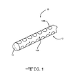
- FIG. 1 illustrates a neural interface system 10 according to the present invention.
- the neural interface system 10 comprises an electrode array 12 having a plurality of electrode sites 14A and 14B.
- the electrodes may be adapted to optimally sample (record) 14A or selectively activate (stimulate) 14B neural populations and may be individually or simultaneously activatable to create an activation pattern.
- the neural interface system 10 may further include a pre-molded component 15 onto which the neural interface array is attached or assembled that supports the electrode array 12.
- the electrode array 12 is coupled to the pre-molded component 15 such that the electrodes 14A, 14B are arranged both circumferentially around and axially there along.
- the neural interface system 10 of the present invention is preferably designed for deep brain stimulation and, more specifically, for deep brain stimulation with fine electrode site positioning, selectivity, tunability, and precise activation patterning.
- the neural interface system 10 may be alternatively used in any suitable environment (such as the spinal cord, peripheral nerve, muscle, or any other suitable anatomical location) and for any suitable reason.
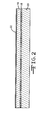
- FIG. 2 shows the dielectric substrate 16 contacting a release layer 18 that is directly supported on a carrier 20.
- the dielectric layer 16 can be of a flexible thin material, preferably parylene, polyimide, silicon, or even a thin-film of silicon, or some combination of organic and inorganic dielectrics, but may alternatively be of any suitable material.
- the carrier 20 is preferably made of glass or silicon, but may alternatively be made from any other suitable material.
- the carrier 20 is may be flexible, rigid, or semi rigid depending on the microfabrication tooling (organic electronics equipment can increasingly use flexible substrates, whereas IC and MEMS microfabrication equipment use rigid silicon).
- a rigid carrier layer 20 has a thickness ranging from about 200 microns to about 925 microns, preferably greater than 500 microns.
- a metallization layer 22 is deposited on the upper or outer surface 16A of the dielectric substrate 16.
- the metallization 22 is shown as a continuous layer having a perimeter extending from a lower metallization surface supported on the upper substrate surface 16A to an upper metallization surface spaced from the lower metallization surface by a thickness of the perimeter.
- the metallization is substantially contiguous with the width and length (x- and y-axes) of the dielectric layer 16, although that is not necessary.
- the metallizations 22 can be deposited using any suitable thin film, semiconductor, microelectromechanical systems (MEMS) manufacturing technique or other microfabrication process, such as vapor deposition. Exemplary techniques and processes include evaporation and sputtering deposition.
- the metallizations layer 22 preferably includes a conductive material such as of gold (Au), platinum (Pt) or platinum-iridium, or any other metal, metal oxide, or conductive polymer having suitable electrically conductive properties.
- FIG. 3 shows where the continuous metallization 22 has been patterned into a plurality of discrete metallization structures 22A, 22B, 22C, 22D, 22E, etc.
- the metallization layer 22 can be patterned through etching, liftoff deposition, or any other suitable thin film, semiconductor manufacturing, MEMS manufacturing, or other microfabrication process.
- the dielectric substrate 16, the release layer 18 and the carrier 20 can be flexible, semi-flexible, or rigid.
- the present method can further include patterning the metallization structures 22A, 22B, 22C, 22D, 22E, etc. to include conductive traces, bond pads, and other suitable conductive elements.
- a layer of nanospheres 26 has been deposited onto the dielectric substrate 16 to cover both the shaped metallizations 22A, 22B, 22C, 22D, 22E, etc. and the substrate surface 16A between adjacent metallizations.
- the nanospheres 26 form a high-density, high-resolution spatial pattern serving as a substantially uniform mask or template over the surface of the individual metallizations. That is because the nanospheres 26 are substantially identical in size and shape.
- the nanospheres 26 self-assemble into a tightly packed, uniform pattern.
- the present method can include depositing a monolayer of nanospheres 26 onto the metallizations 22A, 22B, 22C, 22D, 22E, etc. by drop wetting (direct application of the nanospheres in solution) and then allowing them to self-assemble into hexagonally packed patterns ( FIG. 8 ) upon de-wetting.
- This embodiment includes depositing a nanosphere solution including nanospheres and a solvent onto the metallization structures 22A, 22B, 22C, 22D, 22E, etc. The solvent is then evaporated.
- the solvent is preferably selected based on its viscosity, evaporation rate, and wettability on the metallizations patterned on the dielectric substrate 16.
- the solution includes polystyrene spheres mixed in a solvent of ethanol and de-ionized water.
- the ratio of ethanol to de-ionized water is approximately 4:1.
- the solution can include nanospheres 26 other than those of polystyrene and a suitable solvent other than a mixture of ethanol and de-ionized water.
- the solution is preferably dropped onto the dielectric substrate 16 such that a monolayer of nanospheres 26 is distributed substantially uniformly on the metallization structures 22A, 22B, 22C, 22D, 22E, etc.
- Depositing the nanosphere solution may be performed by using the Langmuir-Blodgett technique to transfer a pre-fabricated monolayer of nanospheres 26 onto the metallizations 22A, 22B, 22C, 22D, 22E, etc. patterned on the dielectric substrate 16.
- nanospheres 26 having a surface tension of ⁇ -NS are in a solvent having a surface tension of ⁇ -solvent. It is given that ⁇ -NS is less than ⁇ -solvent.
- a monolayer of nanospheres 26 forms at the exposed surface of metallizations 22A, 22B, 22C, 22D, 22E, etc. patterned on the dielectric substrate 16.
- the substrate 16 supported on the release layer 18 and the carrier 20 can be moved through the solution to transfer the monolayer of the nanospheres 26 thereto.
- a nanosphere solution e.g., 5% w/v solution
- the nanospheres 26 When applied to a patterned dielectric substrate 16 at room temperature on a horizontal surface, the nanospheres 26 will self-assemble along a contact line during the evaporation or de-wetting process.
- Evaporation of the solvent can occur unassisted or be accelerated with environmental changes, such as in temperature and pressure from that of an ambient atmosphere.
- a second preferred embodiment is where the nanospheres 26 are deposited onto the metallization structures 22A, 22B, 22C, 22D, 22E, etc. via spin-coating the above described nanosphere solution.
- the nanosphere solution can have a different viscosity, wettability, or other mixture ratio than that used with the drop-wetting or Langmuir-Blodgett technique.
- spin-coating can include a particular rate of spinning and/or acceleration.
- a series of recessed undulations 22A', 22B', 22C', 22D', 22E', etc. or upstanding undulations 22A", 22B" , 22C", 22D", 22E", etc. are formed on the surface of the metallizations 22A, 22B, 22C, 22D, 22E, etc.
- the recessed or upstanding undulations can be approximately pyramidal wave undulations, square wave undulations, approximately triangular wave undulations, or an undulation of any other suitable shape.
- FIGs. 5, 5A and 5A' show recessed undulations 22A', 22B', 22C', 22D', 22E', etc. that have been formed by etching 28 recesses 30 into the thickness of the respective metallizations 22A, 22B, 22C, 22D, 22E, etc. Etching 28 the recesses 30 into the metallizations takes place beneath the interstitial spaces of the layer of assembled nanospheres 26. The result is undulations 22A", 22B", 22C", 22D", 22E", etc. comprising recesses extending into the original thickness or height (h) of the metallization layers supported on the substrate 16.
- the nanospheres 26 a diameter ranging from about 20 nanometer (nm) to about 1,000 nm.
- Etching can be performed with any suitable etching process.
- One advantage of etching is that it does not require any adhesion between the existing metallization layer and newly deposited conductive material.
- Platinum for example, is a commonly used biocompatible metal that can be dry etched using techniques described in U.S. Patent No. 6,323,132 with a reactive ion etcher. The contents of this patent are incorporated herein by reference.
- etching forms the recesses 30 having a depth extending part-way through the thickness of the metallization 22B from that portion of its upper surface of the metallization not contacted or otherwise covered by a nanosphere 26.
- the recesses 30 can extend from about 1% to about 99% into the thickness of the metallizations 22A, 22B, 22C, 22D, 22E, etc. More preferably, the recesses are from about 50% to about 90% into the original metallization thickness.
- the metallizations shown in FIG. 5A have a thickness measured from the upper surface 16A of the dielectric 18 to the upper surface of the as-deposited metallization of from about 0.25 micron to about 20 microns.
- FIGs 6, 6A and 6A' relate to an alternative method where the upstanding undulations 22A", 22B", 22C", 22D", 22E", etc. are formed by depositing 30 additional metallization material (e.g., in a lift-off deposition) onto the metallizations 22A, 22B, 22C, 22D, 22E, etc. through the interstitial spaces between the nanospheres 26. Deposition 30 continues until the desired height of the added metallization material 32 measured from its base 32A supported on the upper surface of the original metallization 22B is achieved. For this technique, it is preferred that that the nanospheres have a diameter ranging from about 500 nm to about 5,000 nm.
- FIG. 7A illustrates a representative one of the undulations where the additional metallization material 32 forms a base on the upper surface of the metallization 22B and build-up in a pyramidal manner. That is without contacting the adjacent nanospheres 26, but while following their generally circular contour.
- the height of the upstanding undulations is preferably about 90% of the radius of the nanosphere. It has been discovered that this ratio provides maximum added surface area for the added metallization. That means the upstanding additional or secondary metallization material has a height ranging from about 225 nm to about 2,250 nm above the upper surface of the primary metallization 22.
- the added metallization does not grow so high as to prevent the subsequent removal of the nanospheres.
- FIG. 7B is a photograph showing how the deposited metallization material builds up from the upper surface of a metallization without contacting the nanospheres 26.
- the nanospheres 26 have been removed in the photograph, but the generally circular shape of one of them is delineated by the circle bordered by the deposited metallization material, which is seen as the off-white pyramidal bodies having somewhat triangular bases.
- the recessed undulations 22A', 22B', 22C', 22D', 22E', etc and extending 22A", 22B", 22C", 22D", 22E", etc on the respective metallizations are preferably bounded by the interstitial spaces of the nanospheres 26. Since the nanospheres 26 are substantially uniform in shape and arranged in a substantially uniform distribution in the layers of FIGs 5 and 6 supported on the upper surface of the metallization 22A, 22B, 22C, 22D, 22E, etc., there is a substantially uniform distribution of interstitial spaces between the nanospheres 26. Consequently, the undulations 22A', 22B', 22C', 22D', 22E', etc. and 22A", 22B", 22C", 22D", 22E", etc. are substantially uniformly distributed throughout the surface area of the shaped metallization.
- the nanospheres 26 are removed from the dielectric substrate 18 after forming recessed or extending the undulations 22A', 22B', 22C', 22D', 22E', etc. and 22A", 22B", 22C", 22D", 22E", etc. on the respective metallizations 22A, 22B, 22C, 22D, 22E, etc. or, the nanospheres 26 can be left on the metallizations.
- the undulations 22A', 22B', 22C', 22D', 22E', etc and 22A", 22B", 22C", 22D", 22E", etc significantly increase the electrochemical surface area (ESA) of the electrode, particularly relative to the geometric surface area (GSA) of an electrode formed from one of the metallization according to the present invention.
- the interstitial spaces of the nanospheres are preferably arranged in a substantially uniform distribution, thereby enabling substantially uniform arrangement of the undulations.
- the undulating surface provides an increased ESA predicated on the diameter and packing arrangement of the nanospheres 26, and the depth of recess 30 for the recessed undulation 22A', 22B', 22C', 22D', 22E', etc. or the increased thickness of the deposited metallization material 32 for the extending undulations 22A", 22B", 22C", 22D", 22E", etc.
- a inc ⁇ 2 ⁇ D s ⁇ d m
- a new_total A e + A inc ⁇ A e
- a new_ratio 1 + 2 ⁇ ⁇ 3 ⁇ d m D s ⁇ 100
- a increase area of ESA increase through either deposition or etching
- D s diameter of a sphere
- d m height of deposition or the depth of etch
- a e geometric are of electrode (derived from the metallizations 22).
- the present invention methods additionally or alternatively include one or more of several variations described below.
- a further according to the present invention includes undercutting one or more alternating layers of patterned metal.
- the method includes: depositing a planar metallization layer stack (e.g., Au/Pt, Au/Ir, or other Au stack) onto the dielectric substrate 16, and then selectively wet etching the Au metal.
- a planar metallization layer stack e.g., Au/Pt, Au/Ir, or other Au stack
- An example of this is to deposit a layer of platinum 40 onto the dielectric layer (not shown in FIG. 10B ) using one of the methods previously described with respect to FIGs. 2A to 2C, 3 and 4 .
- a layer of gold 42 is deposited on top of the platinum 40 followed by a second layer of platinum.
- the nanospheres 26 are then removed and the gold 42 is wet etched. Etching serves to expose additional surface area of the platinum 40 that was previously positioned both above and below the gold. This is shown by the exposed surface 42A of the platinum layers 42 in FIG. 10B .
- d Au the depth of etch is depicted as d Au , which is less than the original thickness of the gold layer measured parallel to the plane of the dielectric substrate 16.
- iridium and titanium nitride are suitable metallization materials for use with this gold etching process. In that manner, gold etching serves to expose more of the non-Au metal surface area.
- FIGs. 11A and 11B relate to another embodiment of the method according to the present invention.
- This embodiment additionally or alternatively includes depositing an alternating combination of layers on the dielectric substrate (not shown in FIG. 11B ).
- alternating layer of platinum 40 and gold 42 are deposited one on top of the other until a stack of a desired height is achieved.
- the gold layers are wet etched to undercut and expose addition platinum surface area. As described above, it is important not to etch too much of the gold 42.
- the depth of etch is depicted as d Au , which is less than the original thickness of the gold layer measured parallel to the plane of the dielectric substrate 16.
- Enough gold must be left to serve as a structural pillar supporting the above platinum and gold layers.
- An example of this embodiment is alternating layers of Au/Pt/Au/Pt/Au/Pt stacked one on top of the other. Gold etching preferably forms more ESA.
- the preferred embodiments of the present methods include every combination and permutation of the various processes described above.
- the preferred embodiments of the present method can be executed by a computer program or other system including computer program code for controlling hardware (e.g., machines for deposition, sputtering) in an automated fashion.
- a neural interface device 10 with reduced impedance includes the dielectric substrate 16 supporting the electrode array 12 comprising the plurality of electrodes 14A, 14B.
- the dielectric substrate 16 is remove from the carrier 20.
- the release layer 18 facilitates this separation.
- the dielectric substrate 16 and the electrode array 12 are then formed into a desired shape of the neural interface system 10, which can be either planar or three-dimensional such as the cylindrical shape shown.
- the neural interface device 10 can be a planar probe with the electrode array 12, a cylindrical probe with the electrode array, a substantially planar or curved substrate with the electrode array, or any suitable electrode device.
- each electrode 14A, 14B has a substantially uniform undulating surface described above. At least a portion of the substantially uniform undulating surfaces of the electrodes 14A, 14B includes peaks and/or crevices (e.g., recesses) that are preferably distributed in a regular arrangement and, more preferably, in an approximately hexagonal arrangement as shown in FIGs. 5A, 5A', 6A and 6A' .
- the undulating surfaces increases the electrochemical surface area of the electrodes 14A, 14B, thereby reducing their impedance and improving their functionality for stimulation and sensing purposes.
Landscapes
- Health & Medical Sciences (AREA)
- Life Sciences & Earth Sciences (AREA)
- Animal Behavior & Ethology (AREA)
- Engineering & Computer Science (AREA)
- Biomedical Technology (AREA)
- Veterinary Medicine (AREA)
- Public Health (AREA)
- General Health & Medical Sciences (AREA)
- Heart & Thoracic Surgery (AREA)
- Radiology & Medical Imaging (AREA)
- Nuclear Medicine, Radiotherapy & Molecular Imaging (AREA)
- Surgery (AREA)
- Physics & Mathematics (AREA)
- Molecular Biology (AREA)
- Medical Informatics (AREA)
- Pathology (AREA)
- Biophysics (AREA)
- Cardiology (AREA)
- Semiconductor Memories (AREA)
- Neurology (AREA)
- Electrodes Of Semiconductors (AREA)
- Electroplating Methods And Accessories (AREA)
Abstract
Description
- This application claims priority from
U.S. Provisional Application Serial Nos. 61/534,787, filed on Sept. 14, 2011 61/535,852, filed on Sept. 16, 2011 - This invention relates generally to the electrode field, and more specifically to new and useful methods for forming an electrode device with reduced impedance. Such electrode are useful when fabricated into neural electrode assemblies for electrically stimulating body tissue or for recording physiological conditions of the body tissue.
- Ideally, conductive electrodes, such as electrodes for sensing and/or stimulation in neural probes, or other neural interface devices, have minimal impedance magnitude and impedance variance (e.g., for an electrode at different times). High impedance generally corresponds with several disadvantages. Sensing and recording electrodes with high impedance typically experience high thermal noise. Stimulation electrodes with high impedance require larger amounts of power during stimulation. Furthermore, a large amount of variance in impedance typically results in poor reliability and predictability during both sensing and stimulation modes of operation.
- Increasing the geometric surface area or "footprint" of an electrode is one technique to reduce impedance magnitude and variance, but that approach reduces the electrode's spatial resolution. Increasing the electrochemical surface area of an electrode is another technique for reducing impedance magnitude and variance, but at significant cost and resources. Current methods, such as electrodeposition or electroplating, for increasing a neural electrode's electrochemical surface area are often performed post-process on individual devices after microfabrication and, therefore, are relatively expensive. Electrodeposition can also be performed in batch processes, but this usually has issues with uniformity and repeatability. Also, reliability issues, such as changes in the charge carrying capacity over time or delamination between the modified electrode material and the underlying substrate, can be a concern.
- Thus, there is a need in the electrode field to create a new and useful method for reducing the impedance of a neural electrode device. The present invention provides such new and useful methods for manufacturing electrode device, particularly those that are adapted for useful in neural interface applications.
- The present invention relates to improved low-cost, highly reliable methods for increasing the electrochemical surface area of neural electrodes. In particular, the invention relates to the deposition of a mono-layer of polymeric nanospheres on a dielectric substrate. The nanospheres self-assemble into generally repeating lattice forms with interstitial space between them. In one embodiment, the metallization material that is left exposed between adjacent nanospheres is etched. Etching is only part-way through the thickness of the metallization. In another embodiment, metallization material that are suitable for subsequent use as electrode in neural probes, and the like, are deposited on the dielectric substrate, filling in the interstitial space between the arrayed nanospheres. The deposited metallization material builds into pyramidal-type structures that are shaped by the size of the nanospheres and the interstitial spacing between them. The nanospheres are then removed leaving behind the shaped metallization deposits of relatively high surface area. Such metallization deposits help to minimize impedance magnitude and impedance variance from one electrode to the next.
- A further improvement is to deposit alternating layers of metals into the interstitial space between the nanospheres. One of the metals, for example gold, is more readily etched than the other, for example platinum or iridium. The gold layers are then selectively etched to expose additional platinum surface area that was previously covered by the gold. This additional surface area is that which previously had gold both immediately above and below it.
- The present invention will be described by reference to the following drawings, in which like numerals refer to like elements, and in which:
-
FIG. 1 is a perspective view of aneural interface system 10 according to the present invention. -
FIG. 2 is a schematic drawing showing ametallization layer 22 supported on adielectric substrate 16 supported on arelease layer 18 and acarrier layer 20 for forming anelectrode -
FIG. 3 is a schematic drawing showing a plurality ofmetallization layers 22A to 22E that are the result of etching themetallization layer 22 shown inFIG. 2A or after the mask layers 24A to 24F have been removed fromFIG. 2C . -
FIG. 4 is a schematic drawing showing deposition of a mono-layer ofnanospheres 26 being deposited on themetallizations 22A to 22E ofFIG. 3 . -
FIGs. 5, 5A and 5A' are schematic drawings showing a method according to the present invention where undulations are formed in themetallizations 22A to 22E byetching recesses 30 into their thicknesses. -
FIG. 6, 6A and 6A' are schematic drawings showing a method according to the present invention where undulations are formed by depositingmetallization material 32 onto themetallizations 22A to 22E. -
FIG. 7A is a schematic showing deposition ofmetallization material 32 betweenadjacent nanospheres 26. -
FIG. 7B is a partial photographic image of an exemplary electrode resulting from the method of the present invention depicted inFIGs. 6, 6A and 6A' . -
FIG. 8 is a schematic of nanosphere packing and calculation of increased electrochemical surface area resulting from the methods of the present invention. -
FIG. 9 is a table of results from one example of the method of the present invention. -
FIG. 10A are a flow chart of the steps used to increase the effective surface area of depositedplatinum layers 40 by etching anintermediate gold layer 42. -
FIG. 10B is a schematic drawing showing the steps described in the flowchart ofFIG. 10A . -
FIG. 11A are a flow chart of the steps used to increase the effective surface area of depositedplatinum layers 40 by etching anintermediate gold layer 42 in a deposition profile of Pt/Au/Pt/Au/Pt. -
FIG. 11B is a schematic drawing showing the steps described in the flowchart ofFIG. 11A . - The present invention will be described in connection with a preferred embodiments, however, it should be understood that there is no intent to limit the invention to the embodiment described. On the contrary, the intent is to cover all alternatives, modifications, and equivalents as may be included within the scope of the invention as defined by the appended claims.
- The present methods described herein are primarily referenced to forming a single electrode device, and in particular a neural electrode device. However, it should be understood that the present methods can be configured to form a plurality of electrode devices that are suitable for medical sensing or stimulation applications. In a preferred embodiment, the present methods can be adapted to manufacture an electrode that is suitable for any electrical stimulation technology and any recording or sensing technology having conductive electrodes, such as electrodes that are useful in physiological solutions. In that light, the methods described herein are readily adaptable to scaling to batch processes for forming a plurality of electrode devices with reduced impedance at relatively low cost and high uniformity from one electrode to the next.
- Turning now to the drawings,
FIG. 1 illustrates aneural interface system 10 according to the present invention. Theneural interface system 10 comprises anelectrode array 12 having a plurality ofelectrode sites neural interface system 10 may further include apre-molded component 15 onto which the neural interface array is attached or assembled that supports theelectrode array 12. Theelectrode array 12 is coupled to thepre-molded component 15 such that theelectrodes neural interface system 10 of the present invention is preferably designed for deep brain stimulation and, more specifically, for deep brain stimulation with fine electrode site positioning, selectivity, tunability, and precise activation patterning. Theneural interface system 10, however, may be alternatively used in any suitable environment (such as the spinal cord, peripheral nerve, muscle, or any other suitable anatomical location) and for any suitable reason. - Methods for building the
electrode array 12 comprising theelectrodes -
FIG. 2 shows thedielectric substrate 16 contacting arelease layer 18 that is directly supported on acarrier 20. Thedielectric layer 16 can be of a flexible thin material, preferably parylene, polyimide, silicon, or even a thin-film of silicon, or some combination of organic and inorganic dielectrics, but may alternatively be of any suitable material. - The
carrier 20 is preferably made of glass or silicon, but may alternatively be made from any other suitable material. Thecarrier 20 is may be flexible, rigid, or semi rigid depending on the microfabrication tooling (organic electronics equipment can increasingly use flexible substrates, whereas IC and MEMS microfabrication equipment use rigid silicon). Arigid carrier layer 20 has a thickness ranging from about 200 microns to about 925 microns, preferably greater than 500 microns. - A
metallization layer 22 is deposited on the upper orouter surface 16A of thedielectric substrate 16. Themetallization 22 is shown as a continuous layer having a perimeter extending from a lower metallization surface supported on theupper substrate surface 16A to an upper metallization surface spaced from the lower metallization surface by a thickness of the perimeter. The metallization is substantially contiguous with the width and length (x- and y-axes) of thedielectric layer 16, although that is not necessary. Themetallizations 22 can be deposited using any suitable thin film, semiconductor, microelectromechanical systems (MEMS) manufacturing technique or other microfabrication process, such as vapor deposition. Exemplary techniques and processes include evaporation and sputtering deposition. Themetallizations layer 22 preferably includes a conductive material such as of gold (Au), platinum (Pt) or platinum-iridium, or any other metal, metal oxide, or conductive polymer having suitable electrically conductive properties. -
FIG. 3 shows where thecontinuous metallization 22 has been patterned into a plurality ofdiscrete metallization structures metallization layer 22 can be patterned through etching, liftoff deposition, or any other suitable thin film, semiconductor manufacturing, MEMS manufacturing, or other microfabrication process. - Depending on the particular application for the finished
neural interface system 10, thedielectric substrate 16, therelease layer 18 and thecarrier 20 can be flexible, semi-flexible, or rigid. The present method can further include patterning themetallization structures - In
FIG. 4 , a layer ofnanospheres 26 has been deposited onto thedielectric substrate 16 to cover both the shapedmetallizations substrate surface 16A between adjacent metallizations. Thenanospheres 26 form a high-density, high-resolution spatial pattern serving as a substantially uniform mask or template over the surface of the individual metallizations. That is because thenanospheres 26 are substantially identical in size and shape. When they are deposited in a monolayer onto themetallizations nanospheres 26 self-assemble into a tightly packed, uniform pattern. - For example, the present method can include depositing a monolayer of
nanospheres 26 onto themetallizations FIG. 8 ) upon de-wetting. This embodiment includes depositing a nanosphere solution including nanospheres and a solvent onto themetallization structures dielectric substrate 16. - In one illustrative example, the solution includes polystyrene spheres mixed in a solvent of ethanol and de-ionized water. The ratio of ethanol to de-ionized water is approximately 4:1. However, the solution can include
nanospheres 26 other than those of polystyrene and a suitable solvent other than a mixture of ethanol and de-ionized water. The solution is preferably dropped onto thedielectric substrate 16 such that a monolayer ofnanospheres 26 is distributed substantially uniformly on themetallization structures - Depositing the nanosphere solution may be performed by using the Langmuir-Blodgett technique to transfer a pre-fabricated monolayer of
nanospheres 26 onto themetallizations dielectric substrate 16. In an example,nanospheres 26 having a surface tension of γ-NS are in a solvent having a surface tension of γ-solvent. It is given that γ-NS is less than γ-solvent. Then, a monolayer ofnanospheres 26 forms at the exposed surface ofmetallizations dielectric substrate 16. Thesubstrate 16 supported on therelease layer 18 and thecarrier 20 can be moved through the solution to transfer the monolayer of thenanospheres 26 thereto. - Illustratively, one can use the drop wetting method by mixing a nanosphere solution (e.g., 5% w/v solution) into a 4:1 volume mixture of ethanol to de-ionized water. When applied to a patterned
dielectric substrate 16 at room temperature on a horizontal surface, thenanospheres 26 will self-assemble along a contact line during the evaporation or de-wetting process. - Evaporation of the solvent can occur unassisted or be accelerated with environmental changes, such as in temperature and pressure from that of an ambient atmosphere.
- A second preferred embodiment is where the
nanospheres 26 are deposited onto themetallization structures - According to the present invention, a series of recessed
undulations 22A', 22B', 22C', 22D', 22E', etc. orupstanding undulations 22A", 22B" , 22C", 22D", 22E", etc. are formed on the surface of themetallizations -
FIGs. 5, 5A and 5A' show recessed undulations 22A', 22B', 22C', 22D', 22E', etc. that have been formed by etching 28recesses 30 into the thickness of therespective metallizations Etching 28 therecesses 30 into the metallizations takes place beneath the interstitial spaces of the layer of assemblednanospheres 26. The result is undulations 22A", 22B", 22C", 22D", 22E", etc. comprising recesses extending into the original thickness or height (h) of the metallization layers supported on thesubstrate 16. - For etching, it is preferred that the nanospheres 26 a diameter ranging from about 20 nanometer (nm) to about 1,000 nm. Etching can be performed with any suitable etching process. One advantage of etching is that it does not require any adhesion between the existing metallization layer and newly deposited conductive material. Platinum, for example, is a commonly used biocompatible metal that can be dry etched using techniques described in
U.S. Patent No. 6,323,132 with a reactive ion etcher. The contents of this patent are incorporated herein by reference. - In that manner, etching forms the
recesses 30 having a depth extending part-way through the thickness of themetallization 22B from that portion of its upper surface of the metallization not contacted or otherwise covered by ananosphere 26. Therecesses 30 can extend from about 1% to about 99% into the thickness of themetallizations FIG. 5A have a thickness measured from theupper surface 16A of the dielectric 18 to the upper surface of the as-deposited metallization of from about 0.25 micron to about 20 microns. -
FIGs 6, 6A and 6A' relate to an alternative method where theupstanding undulations 22A", 22B", 22C", 22D", 22E", etc. are formed by depositing 30 additional metallization material (e.g., in a lift-off deposition) onto themetallizations nanospheres 26.Deposition 30 continues until the desired height of the addedmetallization material 32 measured from itsbase 32A supported on the upper surface of theoriginal metallization 22B is achieved. For this technique, it is preferred that that the nanospheres have a diameter ranging from about 500 nm to about 5,000 nm. - One advantage of this variation is that depositing material preferably results in metal-metal bonds and predictable surface properties.
FIG. 7A illustrates a representative one of the undulations where theadditional metallization material 32 forms a base on the upper surface of themetallization 22B and build-up in a pyramidal manner. That is without contacting theadjacent nanospheres 26, but while following their generally circular contour. In that respect, the height of the upstanding undulations is preferably about 90% of the radius of the nanosphere. It has been discovered that this ratio provides maximum added surface area for the added metallization. That means the upstanding additional or secondary metallization material has a height ranging from about 225 nm to about 2,250 nm above the upper surface of theprimary metallization 22. - Moreover, the added metallization does not grow so high as to prevent the subsequent removal of the nanospheres. In order for nanosphere removal, it is important that the added metallization not extend past the imaginary equator and over the upper half of the hemisphere. With this rule, it has been determined that approximately a four-fold increase in the geometric surface area (GSA) is achievable.
-
FIG. 7B is a photograph showing how the deposited metallization material builds up from the upper surface of a metallization without contacting thenanospheres 26. Thenanospheres 26 have been removed in the photograph, but the generally circular shape of one of them is delineated by the circle bordered by the deposited metallization material, which is seen as the off-white pyramidal bodies having somewhat triangular bases. - In both embodiments, the recessed
undulations 22A', 22B', 22C', 22D', 22E', etc and extending 22A", 22B", 22C", 22D", 22E", etc on the respective metallizations are preferably bounded by the interstitial spaces of thenanospheres 26. Since thenanospheres 26 are substantially uniform in shape and arranged in a substantially uniform distribution in the layers ofFIGs 5 and6 supported on the upper surface of themetallization nanospheres 26. Consequently, theundulations 22A', 22B', 22C', 22D', 22E', etc. and 22A", 22B", 22C", 22D", 22E", etc. are substantially uniformly distributed throughout the surface area of the shaped metallization. - If desired, the
nanospheres 26 are removed from thedielectric substrate 18 after forming recessed or extending theundulations 22A', 22B', 22C', 22D', 22E', etc. and 22A", 22B", 22C", 22D", 22E", etc. on therespective metallizations nanospheres 26 can be left on the metallizations. - The
undulations 22A', 22B', 22C', 22D', 22E', etc and 22A", 22B", 22C", 22D", 22E", etc significantly increase the electrochemical surface area (ESA) of the electrode, particularly relative to the geometric surface area (GSA) of an electrode formed from one of the metallization according to the present invention. The interstitial spaces of the nanospheres (or "pores" of the layers of the nanospheres) are preferably arranged in a substantially uniform distribution, thereby enabling substantially uniform arrangement of the undulations. - The particular form of the undulation, whether they be of the recessed or the extending form (etching or deposition) of the metallizations depends on the functional application of the electrode that will be manufactured from the metallization device, desired dimensions of the electrode, extensions, and/or recesses, materials within the metallization, and/or any suitable factor. In any event, the undulating surface provides an increased ESA predicated on the diameter and packing arrangement of the
nanospheres 26, and the depth ofrecess 30 for the recessedundulation 22A', 22B', 22C', 22D', 22E', etc. or the increased thickness of the depositedmetallization material 32 for the extendingundulations 22A", 22B", 22C", 22D", 22E", etc. - As shown in
FIG. 8 , the amount that the ESA increases as is inversely proportional to the diameter of the sphere:


where Aincrease = area of ESA increase through either deposition or etching, Ds = diameter of a sphere, dm = height of deposition or the depth of etch, and Ae = geometric are of electrode (derived from the metallizations 22). Estimated area change and estimated reductions of impedance in various illustrative examples of etched metallization electrode sites (Figs, 5, 5A and 5A' ) are shown in Table 1 ofFIG. 9 . - In some preferred embodiments, the present invention methods additionally or alternatively include one or more of several variations described below.
- As shown in
FIGs. 10A and 10B , a further according to the present invention includes undercutting one or more alternating layers of patterned metal. In one version of this embodiment, the method includes: depositing a planar metallization layer stack (e.g., Au/Pt, Au/Ir, or other Au stack) onto thedielectric substrate 16, and then selectively wet etching the Au metal. - An example of this is to deposit a layer of
platinum 40 onto the dielectric layer (not shown inFIG. 10B ) using one of the methods previously described with respect toFIGs. 2A to 2C, 3 and 4 . Without removing thenanospheres 26, a layer ofgold 42 is deposited on top of theplatinum 40 followed by a second layer of platinum. Thenanospheres 26 are then removed and thegold 42 is wet etched. Etching serves to expose additional surface area of theplatinum 40 that was previously positioned both above and below the gold. This is shown by the exposed surface 42A of the platinum layers 42 inFIG. 10B . - It is important to not etch too much of the
gold 42 so that it can no longer act as a structural support for theplatinum 40. InFIG. 10B , the depth of etch is depicted as dAu, which is less than the original thickness of the gold layer measured parallel to the plane of thedielectric substrate 16. In addition to platinum, iridium and titanium nitride are suitable metallization materials for use with this gold etching process. In that manner, gold etching serves to expose more of the non-Au metal surface area. -
FIGs. 11A and 11B relate to another embodiment of the method according to the present invention. This embodiment additionally or alternatively includes depositing an alternating combination of layers on the dielectric substrate (not shown inFIG. 11B ). In one specific embodiment alternating layer ofplatinum 40 andgold 42 are deposited one on top of the other until a stack of a desired height is achieved. In a similar manner as described above with respect toFIGs. 10A and 10B , the gold layers are wet etched to undercut and expose addition platinum surface area. As described above, it is important not to etch too much of thegold 42. InFIG. 11B , the depth of etch is depicted as dAu, which is less than the original thickness of the gold layer measured parallel to the plane of thedielectric substrate 16. Enough gold must be left to serve as a structural pillar supporting the above platinum and gold layers. An example of this embodiment is alternating layers of Au/Pt/Au/Pt/Au/Pt stacked one on top of the other. Gold etching preferably forms more ESA. - Although omitted for clarity, the preferred embodiments of the present methods include every combination and permutation of the various processes described above. Furthermore, the preferred embodiments of the present method can be executed by a computer program or other system including computer program code for controlling hardware (e.g., machines for deposition, sputtering) in an automated fashion.
- As previously discussed with respect to
FIG. 1 , aneural interface device 10 with reduced impedance according to the present invention includes thedielectric substrate 16 supporting theelectrode array 12 comprising the plurality ofelectrodes metallization material 22 has been provided with an undulating surface characteristic, whether the undulations are recessed or upstanding, thedielectric substrate 16 is remove from thecarrier 20. Therelease layer 18 facilitates this separation. Thedielectric substrate 16 and theelectrode array 12 are then formed into a desired shape of theneural interface system 10, which can be either planar or three-dimensional such as the cylindrical shape shown. Theneural interface device 10 can be a planar probe with theelectrode array 12, a cylindrical probe with the electrode array, a substantially planar or curved substrate with the electrode array, or any suitable electrode device. - At least a portion of each
electrode electrodes FIGs. 5A, 5A', 6A and 6A' . The undulating surfaces increases the electrochemical surface area of theelectrodes - While this invention has been described in conjunction with preferred embodiments thereof, it is evident that many alternatives, modifications, and variations will be apparent to those skilled in the art. Accordingly, the present invention is intended to embrace all such alternatives, modifications and variations that fall within the broad scope of the appended claims.
Claims (15)
- A neural interface system (10), which comprises:a) a substrate (16);b) at least one primary metallization supported on the substrate (16), wherein the primary metallization (22) has a perimeter extending from a lower metallization surface supported on the substrate (16) to an upper metallization surface spaced from the lower metallization surface by a thickness of the perimeter, wherein the upper surface of the primary metallization (22) is characterized by a plurality of undulating structures, andc) wherein the substrate (16) supporting the primary metallization (22) with the undulating structures on its upper metallization surface thereof is provided in a shape that is suitable for contact with body tissue.
- The neural interface system of claim 1, wherein the substrate (16) is of a dielectric material selected from the group consisting of parylene, polyimide, and silicon.
- The neural interface system of claim 1 or claim 2, wherein the primary metallization (22) is of a material selected from the groups consisting of gold, platinum, and platinum/iridium alloy; preferably wherein the thickness of the primary metallization (22) ranges from 0.25 µm (micron) to 20 µm (microns).
- The neural interface system of any of the claims 1 to 3, wherein the undulating structures comprise a plurality of recesses (30) extending part way into the thickness of the primary metallization (22); preferably wherein the recesses (30) extend from 50% to 90% into the thickness of the primary metallization (22) from the upper surface thereof and are not in communication with each other.
- The neural interface system of any of the claims 1 to 4, wherein the undulating structures comprise a plurality of upstanding secondary metallizations supported on the upper surface of the primary metallization (22), preferably wherein a second thickness of the upstanding secondary metallizations ranges from 225 nm to 2,250 nm above the upper surface of the primary metallization (22).
- The neural interface system of any of the claims 1 to 5, wherein the primary metallization and the second metallization are of the same material or are of different materials.
- A method for providing a neural interface system (10), comprising the steps of:a) providing a substrate (16);b) depositing at least one primary metallization (22) supported on the substrate (16), the primary metallization (22) comprising a perimeter extending from a lower metallization surface supported on the substrate (16) to an upper metallization surface spaced from the lower metallization surface by a thickness of the perimeter;c) depositing a monolayer of nanospheres (26) contacting the upper surface of the metallization (22), andd) treating the upper surface of the primary metallization (22) not contacted by the nanospheres (26) to thereby provide a plurality of undulating structures.
- The method of claim 7, including providing the thickness of the primary metallization (22) ranging from 0.25 µm (micron) to 20 µm (microns).
- The method of claim 7 or claim 8, including providing the nanospheres (26) are comprised of polystyrene; and/or including providing the nanospheres (26) having a diameter ranging from 20 nm to 1,000 nm.
- The method of any of the claims 7 to 9, including mixing the nanospheres (26) with ethanol and de-ionized water to form a nanosphere solution that is deposited on the primary metallizations (22).
- The method of any of the claims 7 to 10, including providing the undulating structures by etching recesses (30) part-way through the thickness of the metallization from the upper surface thereof; preferably including providing the recesses (30) extending from 50% to 90% into the thickness of the primary metallization (22) from the upper surface thereof and not being in communication with each other.
- The method of any of the claims 7 to 11, including depositing a second metallization on the primary metallization (22) to thereby provide the undulating structures; preferably including providing the nanospheres (26) having a diameter ranging from 500 nm to 5,000 nm.
- The method of claim 12, including providing a second thickness of the upstanding secondary metallizations ranging from 225 nm to 2,250 nm above the upper surface of the primary metallization (22); and/or including discontinuing deposition of the secondary metallization when its thickness has reached about 90% of a radius of the nanospheres (26).
- The method of any of the claims 7 to 13, including:i) depositing a relatively more etchable second metallization material on the primary metallization (22), followed by depositing a relatively less etchable tertiary metallization material on the second metallization material to thereby form a metallization stack; andii) etching the metallization stack to remove a portion of the second metallization so that a greater surface area of the primary and tertiary metallization materials is obtained.
- The method of claim 14, including the primary and tertiary metallization materials being the same of different; preferably including providing the primary and tertiary metallization materials being platinum and the secondary metallization material being gold.
Applications Claiming Priority (2)
| Application Number | Priority Date | Filing Date | Title |
|---|---|---|---|
| US201161534787P | 2011-09-14 | 2011-09-14 | |
| US201161535852P | 2011-09-16 | 2011-09-16 |
Publications (2)
| Publication Number | Publication Date |
|---|---|
| EP2570153A1 true EP2570153A1 (en) | 2013-03-20 |
| EP2570153B1 EP2570153B1 (en) | 2017-09-13 |
Family
ID=46888883
Family Applications (1)
| Application Number | Title | Priority Date | Filing Date |
|---|---|---|---|
| EP12006458.9A Not-in-force EP2570153B1 (en) | 2011-09-14 | 2012-09-14 | Methods for forming an electrode device with reduced impedance |
Country Status (2)
| Country | Link |
|---|---|
| US (3) | US9192757B2 (en) |
| EP (1) | EP2570153B1 (en) |
Cited By (1)
| Publication number | Priority date | Publication date | Assignee | Title |
|---|---|---|---|---|
| WO2026020046A1 (en) * | 2024-07-18 | 2026-01-22 | Blackrock Microsystems, Inc. | Implantable embedded systems and related manufacturing methods |
Families Citing this family (15)
| Publication number | Priority date | Publication date | Assignee | Title |
|---|---|---|---|---|
| US9192757B2 (en) * | 2011-09-14 | 2015-11-24 | Greatbatch Ltd. | Methods for forming an electrode device with reduced impedance |
| US11229789B2 (en) | 2013-05-30 | 2022-01-25 | Neurostim Oab, Inc. | Neuro activator with controller |
| EP3441109A1 (en) | 2013-05-30 | 2019-02-13 | Graham H. Creasey | Flexible dermal patch for a topical nerve stimulator system |
| US10173051B2 (en) | 2013-10-21 | 2019-01-08 | Neuronexus Technologies, Inc. | Neural electrode system with a carrier having a tape spring-type shape |
| TWI569771B (en) * | 2014-10-31 | 2017-02-11 | 國立清華大學 | Stereoelectrode with cell affinity and capacitive coupling and biological probe containing the same |
| US11077301B2 (en) | 2015-02-21 | 2021-08-03 | NeurostimOAB, Inc. | Topical nerve stimulator and sensor for bladder control |
| KR102382737B1 (en) * | 2015-03-04 | 2022-04-06 | 한국전자통신연구원 | Method for surface modification of neural electrode |
| WO2016205610A1 (en) * | 2015-06-18 | 2016-12-22 | The University Of Florida Research Foundation, Inc. | 2d tunable nanosphere lithography of nanostructures |
| CA3014910A1 (en) | 2016-02-22 | 2017-08-31 | The Charles Stark Draper Laboratory, Inc. | Method of manufacturing an implantable neural electrode interface platform |
| DE102016222710A1 (en) * | 2016-11-18 | 2018-05-24 | Neuroloop GmbH | Implantable electrical contact arrangement |
| US11134868B2 (en) | 2017-03-17 | 2021-10-05 | Medtronic Minimed, Inc. | Metal pillar device structures and methods for making and using them in electrochemical and/or electrocatalytic applications |
| EP3706856A4 (en) | 2017-11-07 | 2021-08-18 | Neurostim Oab, Inc. | Non-invasive nerve activator with adaptive circuit |
| US11458311B2 (en) | 2019-06-26 | 2022-10-04 | Neurostim Technologies Llc | Non-invasive nerve activator patch with adaptive circuit |
| US11523757B2 (en) | 2019-08-01 | 2022-12-13 | Medtronic Minimed, Inc. | Micro-pillar working electrodes design to reduce backflow of hydrogen peroxide in glucose sensor |
| EP4017580A4 (en) | 2019-12-16 | 2023-09-06 | Neurostim Technologies LLC | NON-INVASIVE NERVE ACTIVATOR WITH AMPLIFIED CHARGE DISTRIBUTION |
Citations (2)
| Publication number | Priority date | Publication date | Assignee | Title |
|---|---|---|---|---|
| US6323132B1 (en) | 1998-01-13 | 2001-11-27 | Applied Materials, Inc. | Etching methods for anisotropic platinum profile |
| WO2011084450A1 (en) * | 2009-12-16 | 2011-07-14 | The Board Of Trustees Of The University Of Illinois | Electrophysiology in-vivo using conformal electronics |
Family Cites Families (23)
| Publication number | Priority date | Publication date | Assignee | Title |
|---|---|---|---|---|
| US6350388B1 (en) * | 1999-08-19 | 2002-02-26 | Micron Technology, Inc. | Method for patterning high density field emitter tips |
| WO2002087685A2 (en) * | 2001-05-01 | 2002-11-07 | Second Sight, Llc | High-density array of micro-machined electrodes for neural stimulation |
| JP4651665B2 (en) * | 2004-07-22 | 2011-03-16 | ユニベルジテート コンスタンツ | Information storage medium |
| WO2008035285A2 (en) * | 2006-09-22 | 2008-03-27 | Koninklijke Philips Electronics N.V. | Implantable multi-electrode device |
| EP2035079B1 (en) * | 2006-06-19 | 2020-09-02 | Second Sight Medical Products, Inc. | Electrode with increased stability and method of manufacturing the same |
| US8731673B2 (en) | 2007-02-26 | 2014-05-20 | Sapiens Steering Brain Stimulation B.V. | Neural interface system |
| US8565894B2 (en) | 2007-10-17 | 2013-10-22 | Neuronexus Technologies, Inc. | Three-dimensional system of electrode leads |
| US8774890B2 (en) * | 2008-03-28 | 2014-07-08 | Georgia Tech Research Corporation | Electrode arrays and methods of making and using same |
| US8886279B2 (en) * | 2008-06-03 | 2014-11-11 | University Of Utah Research Foundation | High aspect ratio microelectrode arrays enabled to have customizable lengths and methods of making the same |
| US8636884B2 (en) * | 2008-09-15 | 2014-01-28 | Abbott Diabetes Care Inc. | Cationic polymer based wired enzyme formulations for use in analyte sensors |
| US8781576B2 (en) * | 2009-03-17 | 2014-07-15 | Cardiothrive, Inc. | Device and method for reducing patient transthoracic impedance for the purpose of delivering a therapeutic current |
| WO2011053254A1 (en) * | 2009-10-30 | 2011-05-05 | Agency For Science, Technology And Research | Probe element and method of forming a probe element |
| US20110288391A1 (en) * | 2010-05-19 | 2011-11-24 | Purdue Research Foundation | Titanium-Based Multi-Channel Microelectrode Array for Electrophysiological Recording and Stimulation of Neural Tissue |
| JP5918778B2 (en) * | 2010-11-15 | 2016-05-18 | アメリカ合衆国 | Perforated contact electrodes on vertical nanowire arrays |
| EP2736402B1 (en) * | 2011-07-25 | 2018-01-10 | NeuroNexus Technologies, Inc. | Opto-electrical device and method for artifact reduction |
| US9192757B2 (en) * | 2011-09-14 | 2015-11-24 | Greatbatch Ltd. | Methods for forming an electrode device with reduced impedance |
| KR20130057721A (en) * | 2011-11-24 | 2013-06-03 | 한국전자통신연구원 | Biosensor, apparatus for detecting biomolecules using the biosensor and detecting method the same |
| US9242087B2 (en) * | 2012-06-01 | 2016-01-26 | The Regents Of The University Of Michigan | Nanocomposites for neural prosthetics devices |
| JP5814868B2 (en) * | 2012-06-29 | 2015-11-17 | 株式会社東芝 | Method for manufacturing magnetic recording medium |
| CA2879831C (en) * | 2012-07-16 | 2019-04-30 | Diagnostic Biochips, Llc | In vivo aptamer-based biosensor |
| KR20150046878A (en) * | 2013-10-23 | 2015-05-04 | 한국전자통신연구원 | Mesoporous neuronal electrode using surfactant of making the same |
| KR102382737B1 (en) * | 2015-03-04 | 2022-04-06 | 한국전자통신연구원 | Method for surface modification of neural electrode |
| FR3055706B1 (en) * | 2016-09-05 | 2018-09-07 | Commissariat A L'energie Atomique Et Aux Energies Alternatives | ANTIREFLECTIVE, STRUCTURED AND HIGHLY LIFETIME OPTICAL SURFACE, AND METHOD FOR CARRYING OUT THE SAME |
-
2012
- 2012-09-14 US US13/617,355 patent/US9192757B2/en active Active
- 2012-09-14 EP EP12006458.9A patent/EP2570153B1/en not_active Not-in-force
-
2015
- 2015-11-16 US US14/941,784 patent/US10052476B2/en active Active
-
2018
- 2018-08-20 US US15/999,381 patent/US11096614B2/en not_active Expired - Fee Related
Patent Citations (2)
| Publication number | Priority date | Publication date | Assignee | Title |
|---|---|---|---|---|
| US6323132B1 (en) | 1998-01-13 | 2001-11-27 | Applied Materials, Inc. | Etching methods for anisotropic platinum profile |
| WO2011084450A1 (en) * | 2009-12-16 | 2011-07-14 | The Board Of Trustees Of The University Of Illinois | Electrophysiology in-vivo using conformal electronics |
Non-Patent Citations (1)
| Title |
|---|
| ANDREAS FROMMHOLD: "NANOTEXTURIZATION OF GOLD SURFACES AND ITS APPLICATION TO NEURAL IMPLANTS", August 2010 (2010-08-01), XP055045985, Retrieved from the Internet <URL:http://etheses.bham.ac.uk/1330/1/Frommhold11PhD.pdf> [retrieved on 20121129] * |
Cited By (1)
| Publication number | Priority date | Publication date | Assignee | Title |
|---|---|---|---|---|
| WO2026020046A1 (en) * | 2024-07-18 | 2026-01-22 | Blackrock Microsystems, Inc. | Implantable embedded systems and related manufacturing methods |
Also Published As
| Publication number | Publication date |
|---|---|
| US20130066182A1 (en) | 2013-03-14 |
| US20190038892A1 (en) | 2019-02-07 |
| US9192757B2 (en) | 2015-11-24 |
| US10052476B2 (en) | 2018-08-21 |
| US11096614B2 (en) | 2021-08-24 |
| EP2570153B1 (en) | 2017-09-13 |
| US20160067473A1 (en) | 2016-03-10 |
Similar Documents
| Publication | Publication Date | Title |
|---|---|---|
| EP2570153B1 (en) | Methods for forming an electrode device with reduced impedance | |
| US8865288B2 (en) | Micro-needle arrays having non-planar tips and methods of manufacture thereof | |
| US20090301994A1 (en) | Methods for Wafer Scale Processing of Needle Array Devices | |
| US7951300B2 (en) | Water-scale needle array | |
| US11013437B2 (en) | Nanopatterned biosensor electrode for enhanced sensor signal and sensitivity | |
| EP1967581B1 (en) | CMOS compatible method for manufacturing microneedle structures | |
| Bhandari et al. | A novel method of fabricating convoluted shaped electrode arrays for neural and retinal prostheses | |
| US9867979B2 (en) | Three-dimensional multi-electrode array | |
| US10856764B2 (en) | Method for forming a multielectrode conformal penetrating array | |
| EP2343550A1 (en) | Improved microneedle | |
| US7922927B2 (en) | Method of forming one or more nanopores for aligning molecules for molecular electronics | |
| US10775335B2 (en) | Nanopatterned biosensor electrode for enhanced sensor signal and sensitivity | |
| US20130224394A1 (en) | Method for producing a capacitor including an array of nanocapacitors | |
| CN112717273A (en) | Nerve electrical stimulation electrode with micro-columnar structure and preparation method thereof | |
| JP2022536660A (en) | Microelectromechanical system structures and their applications | |
| CN107210319A (en) | Large-scale low-cost nano-sensor, nanoneedle and nanometer pumping array | |
| Bhandari et al. | Wafer-scale processed, low impedance, neural arrays with varying length microelectrodes | |
| Bhandari et al. | Wafer level processing of silicon arrays for implantable medical devices | |
| Wu et al. | Microfabrication of high-density microelectrode arrays for peripheral intraneural applications | |
| Yao et al. | Design and Fabrication of Micro Multi-Probe Electrode Arrays | |
| Gunning et al. | High spatial resolution probes for neurobiology applications | |
| Ceyssens et al. | In-situ Growth of Platinum with Hierarchical Porosity for Low Impedance Biomedical Microelectrode Fabrication | |
| SE532576C2 (en) | Method for manufacturing devices for electrical measurements |
Legal Events
| Date | Code | Title | Description |
|---|---|---|---|
| PUAI | Public reference made under article 153(3) epc to a published international application that has entered the european phase |
Free format text: ORIGINAL CODE: 0009012 |
|
| AK | Designated contracting states |
Kind code of ref document: A1 Designated state(s): AL AT BE BG CH CY CZ DE DK EE ES FI FR GB GR HR HU IE IS IT LI LT LU LV MC MK MT NL NO PL PT RO RS SE SI SK SM TR |
|
| AX | Request for extension of the european patent |
Extension state: BA ME |
|
| 17P | Request for examination filed |
Effective date: 20130920 |
|
| RBV | Designated contracting states (corrected) |
Designated state(s): AL AT BE BG CH CY CZ DE DK EE ES FI FR GB GR HR HU IE IS IT LI LT LU LV MC MK MT NL NO PL PT RO RS SE SI SK SM TR |
|
| 17Q | First examination report despatched |
Effective date: 20140930 |
|
| RAP1 | Party data changed (applicant data changed or rights of an application transferred) |
Owner name: GREATBATCH LTD. |
|
| RAP1 | Party data changed (applicant data changed or rights of an application transferred) |
Owner name: NEURONEXUS TECHNOLOGIES, INC. |
|
| GRAP | Despatch of communication of intention to grant a patent |
Free format text: ORIGINAL CODE: EPIDOSNIGR1 |
|
| RIC1 | Information provided on ipc code assigned before grant |
Ipc: A61B 5/04 20060101ALN20161021BHEP Ipc: A61N 1/36 20060101ALN20161021BHEP Ipc: A61N 1/05 20060101AFI20161021BHEP |
|
| GRAJ | Information related to disapproval of communication of intention to grant by the applicant or resumption of examination proceedings by the epo deleted |
Free format text: ORIGINAL CODE: EPIDOSDIGR1 |
|
| INTG | Intention to grant announced |
Effective date: 20161125 |
|
| INTC | Intention to grant announced (deleted) | ||
| GRAP | Despatch of communication of intention to grant a patent |
Free format text: ORIGINAL CODE: EPIDOSNIGR1 |
|
| RIC1 | Information provided on ipc code assigned before grant |
Ipc: A61N 1/05 20060101AFI20170118BHEP Ipc: A61B 5/04 20060101ALN20170118BHEP Ipc: A61N 1/36 20060101ALN20170118BHEP |
|
| GRAJ | Information related to disapproval of communication of intention to grant by the applicant or resumption of examination proceedings by the epo deleted |
Free format text: ORIGINAL CODE: EPIDOSDIGR1 |
|
| INTG | Intention to grant announced |
Effective date: 20170206 |
|
| GRAP | Despatch of communication of intention to grant a patent |
Free format text: ORIGINAL CODE: EPIDOSNIGR1 |
|
| INTC | Intention to grant announced (deleted) | ||
| RIC1 | Information provided on ipc code assigned before grant |
Ipc: A61N 1/05 20060101AFI20170309BHEP Ipc: A61B 5/04 20060101ALN20170309BHEP Ipc: A61N 1/36 20060101ALN20170309BHEP |
|
| INTG | Intention to grant announced |
Effective date: 20170327 |
|
| RAP1 | Party data changed (applicant data changed or rights of an application transferred) |
Owner name: NEURONEXUS TECHNOLOGIES, INC. |
|
| GRAS | Grant fee paid |
Free format text: ORIGINAL CODE: EPIDOSNIGR3 |
|
| GRAA | (expected) grant |
Free format text: ORIGINAL CODE: 0009210 |
|
| AK | Designated contracting states |
Kind code of ref document: B1 Designated state(s): AL AT BE BG CH CY CZ DE DK EE ES FI FR GB GR HR HU IE IS IT LI LT LU LV MC MK MT NL NO PL PT RO RS SE SI SK SM TR |
|
| REG | Reference to a national code |
Ref country code: GB Ref legal event code: FG4D |
|
| REG | Reference to a national code |
Ref country code: CH Ref legal event code: EP |
|
| REG | Reference to a national code |
Ref country code: FR Ref legal event code: PLFP Year of fee payment: 6 |
|
| REG | Reference to a national code |
Ref country code: IE Ref legal event code: FG4D |
|
| REG | Reference to a national code |
Ref country code: AT Ref legal event code: REF Ref document number: 927555 Country of ref document: AT Kind code of ref document: T Effective date: 20171015 |
|
| REG | Reference to a national code |
Ref country code: DE Ref legal event code: R096 Ref document number: 602012037186 Country of ref document: DE |
|
| REG | Reference to a national code |
Ref country code: NL Ref legal event code: MP Effective date: 20170913 |
|
| REG | Reference to a national code |
Ref country code: LT Ref legal event code: MG4D |
|
| PG25 | Lapsed in a contracting state [announced via postgrant information from national office to epo] |
Ref country code: FI Free format text: LAPSE BECAUSE OF FAILURE TO SUBMIT A TRANSLATION OF THE DESCRIPTION OR TO PAY THE FEE WITHIN THE PRESCRIBED TIME-LIMIT Effective date: 20170913 Ref country code: SE Free format text: LAPSE BECAUSE OF FAILURE TO SUBMIT A TRANSLATION OF THE DESCRIPTION OR TO PAY THE FEE WITHIN THE PRESCRIBED TIME-LIMIT Effective date: 20170913 Ref country code: HR Free format text: LAPSE BECAUSE OF FAILURE TO SUBMIT A TRANSLATION OF THE DESCRIPTION OR TO PAY THE FEE WITHIN THE PRESCRIBED TIME-LIMIT Effective date: 20170913 Ref country code: LT Free format text: LAPSE BECAUSE OF FAILURE TO SUBMIT A TRANSLATION OF THE DESCRIPTION OR TO PAY THE FEE WITHIN THE PRESCRIBED TIME-LIMIT Effective date: 20170913 Ref country code: NO Free format text: LAPSE BECAUSE OF FAILURE TO SUBMIT A TRANSLATION OF THE DESCRIPTION OR TO PAY THE FEE WITHIN THE PRESCRIBED TIME-LIMIT Effective date: 20171213 |
|
| REG | Reference to a national code |
Ref country code: AT Ref legal event code: MK05 Ref document number: 927555 Country of ref document: AT Kind code of ref document: T Effective date: 20170913 |
|
| PG25 | Lapsed in a contracting state [announced via postgrant information from national office to epo] |
Ref country code: ES Free format text: LAPSE BECAUSE OF FAILURE TO SUBMIT A TRANSLATION OF THE DESCRIPTION OR TO PAY THE FEE WITHIN THE PRESCRIBED TIME-LIMIT Effective date: 20170913 Ref country code: GR Free format text: LAPSE BECAUSE OF FAILURE TO SUBMIT A TRANSLATION OF THE DESCRIPTION OR TO PAY THE FEE WITHIN THE PRESCRIBED TIME-LIMIT Effective date: 20171214 Ref country code: RS Free format text: LAPSE BECAUSE OF FAILURE TO SUBMIT A TRANSLATION OF THE DESCRIPTION OR TO PAY THE FEE WITHIN THE PRESCRIBED TIME-LIMIT Effective date: 20170913 Ref country code: LV Free format text: LAPSE BECAUSE OF FAILURE TO SUBMIT A TRANSLATION OF THE DESCRIPTION OR TO PAY THE FEE WITHIN THE PRESCRIBED TIME-LIMIT Effective date: 20170913 Ref country code: BG Free format text: LAPSE BECAUSE OF FAILURE TO SUBMIT A TRANSLATION OF THE DESCRIPTION OR TO PAY THE FEE WITHIN THE PRESCRIBED TIME-LIMIT Effective date: 20171213 |
|
| PG25 | Lapsed in a contracting state [announced via postgrant information from national office to epo] |
Ref country code: NL Free format text: LAPSE BECAUSE OF FAILURE TO SUBMIT A TRANSLATION OF THE DESCRIPTION OR TO PAY THE FEE WITHIN THE PRESCRIBED TIME-LIMIT Effective date: 20170913 |
|
| PG25 | Lapsed in a contracting state [announced via postgrant information from national office to epo] |
Ref country code: PL Free format text: LAPSE BECAUSE OF FAILURE TO SUBMIT A TRANSLATION OF THE DESCRIPTION OR TO PAY THE FEE WITHIN THE PRESCRIBED TIME-LIMIT Effective date: 20170913 Ref country code: RO Free format text: LAPSE BECAUSE OF FAILURE TO SUBMIT A TRANSLATION OF THE DESCRIPTION OR TO PAY THE FEE WITHIN THE PRESCRIBED TIME-LIMIT Effective date: 20170913 Ref country code: CZ Free format text: LAPSE BECAUSE OF FAILURE TO SUBMIT A TRANSLATION OF THE DESCRIPTION OR TO PAY THE FEE WITHIN THE PRESCRIBED TIME-LIMIT Effective date: 20170913 |
|
| REG | Reference to a national code |
Ref country code: CH Ref legal event code: PL |
|
| PG25 | Lapsed in a contracting state [announced via postgrant information from national office to epo] |
Ref country code: SK Free format text: LAPSE BECAUSE OF FAILURE TO SUBMIT A TRANSLATION OF THE DESCRIPTION OR TO PAY THE FEE WITHIN THE PRESCRIBED TIME-LIMIT Effective date: 20170913 Ref country code: AT Free format text: LAPSE BECAUSE OF FAILURE TO SUBMIT A TRANSLATION OF THE DESCRIPTION OR TO PAY THE FEE WITHIN THE PRESCRIBED TIME-LIMIT Effective date: 20170913 Ref country code: EE Free format text: LAPSE BECAUSE OF FAILURE TO SUBMIT A TRANSLATION OF THE DESCRIPTION OR TO PAY THE FEE WITHIN THE PRESCRIBED TIME-LIMIT Effective date: 20170913 Ref country code: SM Free format text: LAPSE BECAUSE OF FAILURE TO SUBMIT A TRANSLATION OF THE DESCRIPTION OR TO PAY THE FEE WITHIN THE PRESCRIBED TIME-LIMIT Effective date: 20170913 Ref country code: IS Free format text: LAPSE BECAUSE OF FAILURE TO SUBMIT A TRANSLATION OF THE DESCRIPTION OR TO PAY THE FEE WITHIN THE PRESCRIBED TIME-LIMIT Effective date: 20180113 Ref country code: IT Free format text: LAPSE BECAUSE OF FAILURE TO SUBMIT A TRANSLATION OF THE DESCRIPTION OR TO PAY THE FEE WITHIN THE PRESCRIBED TIME-LIMIT Effective date: 20170913 |
|
| REG | Reference to a national code |
Ref country code: DE Ref legal event code: R097 Ref document number: 602012037186 Country of ref document: DE |
|
| REG | Reference to a national code |
Ref country code: IE Ref legal event code: MM4A |
|
| REG | Reference to a national code |
Ref country code: BE Ref legal event code: MM Effective date: 20170930 |
|
| PG25 | Lapsed in a contracting state [announced via postgrant information from national office to epo] |
Ref country code: MC Free format text: LAPSE BECAUSE OF FAILURE TO SUBMIT A TRANSLATION OF THE DESCRIPTION OR TO PAY THE FEE WITHIN THE PRESCRIBED TIME-LIMIT Effective date: 20170913 Ref country code: LU Free format text: LAPSE BECAUSE OF NON-PAYMENT OF DUE FEES Effective date: 20170914 |
|
| PLBE | No opposition filed within time limit |
Free format text: ORIGINAL CODE: 0009261 |
|
| STAA | Information on the status of an ep patent application or granted ep patent |
Free format text: STATUS: NO OPPOSITION FILED WITHIN TIME LIMIT |
|
| PG25 | Lapsed in a contracting state [announced via postgrant information from national office to epo] |
Ref country code: LI Free format text: LAPSE BECAUSE OF NON-PAYMENT OF DUE FEES Effective date: 20170930 Ref country code: DK Free format text: LAPSE BECAUSE OF FAILURE TO SUBMIT A TRANSLATION OF THE DESCRIPTION OR TO PAY THE FEE WITHIN THE PRESCRIBED TIME-LIMIT Effective date: 20170913 Ref country code: IE Free format text: LAPSE BECAUSE OF NON-PAYMENT OF DUE FEES Effective date: 20170914 Ref country code: CH Free format text: LAPSE BECAUSE OF NON-PAYMENT OF DUE FEES Effective date: 20170930 |
|
| 26N | No opposition filed |
Effective date: 20180614 |
|
| PG25 | Lapsed in a contracting state [announced via postgrant information from national office to epo] |
Ref country code: BE Free format text: LAPSE BECAUSE OF NON-PAYMENT OF DUE FEES Effective date: 20170930 |
|
| REG | Reference to a national code |
Ref country code: FR Ref legal event code: PLFP Year of fee payment: 7 |
|
| PG25 | Lapsed in a contracting state [announced via postgrant information from national office to epo] |
Ref country code: MT Free format text: LAPSE BECAUSE OF NON-PAYMENT OF DUE FEES Effective date: 20170914 |
|
| PG25 | Lapsed in a contracting state [announced via postgrant information from national office to epo] |
Ref country code: SI Free format text: LAPSE BECAUSE OF FAILURE TO SUBMIT A TRANSLATION OF THE DESCRIPTION OR TO PAY THE FEE WITHIN THE PRESCRIBED TIME-LIMIT Effective date: 20170913 |
|
| PG25 | Lapsed in a contracting state [announced via postgrant information from national office to epo] |
Ref country code: HU Free format text: LAPSE BECAUSE OF FAILURE TO SUBMIT A TRANSLATION OF THE DESCRIPTION OR TO PAY THE FEE WITHIN THE PRESCRIBED TIME-LIMIT; INVALID AB INITIO Effective date: 20120914 |
|
| PG25 | Lapsed in a contracting state [announced via postgrant information from national office to epo] |
Ref country code: CY Free format text: LAPSE BECAUSE OF NON-PAYMENT OF DUE FEES Effective date: 20170913 |
|
| PG25 | Lapsed in a contracting state [announced via postgrant information from national office to epo] |
Ref country code: MK Free format text: LAPSE BECAUSE OF FAILURE TO SUBMIT A TRANSLATION OF THE DESCRIPTION OR TO PAY THE FEE WITHIN THE PRESCRIBED TIME-LIMIT Effective date: 20170913 |
|
| PG25 | Lapsed in a contracting state [announced via postgrant information from national office to epo] |
Ref country code: TR Free format text: LAPSE BECAUSE OF FAILURE TO SUBMIT A TRANSLATION OF THE DESCRIPTION OR TO PAY THE FEE WITHIN THE PRESCRIBED TIME-LIMIT Effective date: 20170913 |
|
| PG25 | Lapsed in a contracting state [announced via postgrant information from national office to epo] |
Ref country code: PT Free format text: LAPSE BECAUSE OF FAILURE TO SUBMIT A TRANSLATION OF THE DESCRIPTION OR TO PAY THE FEE WITHIN THE PRESCRIBED TIME-LIMIT Effective date: 20170913 |
|
| PG25 | Lapsed in a contracting state [announced via postgrant information from national office to epo] |
Ref country code: AL Free format text: LAPSE BECAUSE OF FAILURE TO SUBMIT A TRANSLATION OF THE DESCRIPTION OR TO PAY THE FEE WITHIN THE PRESCRIBED TIME-LIMIT Effective date: 20170913 |
|
| PGFP | Annual fee paid to national office [announced via postgrant information from national office to epo] |
Ref country code: GB Payment date: 20220927 Year of fee payment: 11 Ref country code: DE Payment date: 20220928 Year of fee payment: 11 |
|
| PGFP | Annual fee paid to national office [announced via postgrant information from national office to epo] |
Ref country code: FR Payment date: 20220926 Year of fee payment: 11 |
|
| REG | Reference to a national code |
Ref country code: DE Ref legal event code: R119 Ref document number: 602012037186 Country of ref document: DE |
|
| GBPC | Gb: european patent ceased through non-payment of renewal fee |
Effective date: 20230914 |
|
| PG25 | Lapsed in a contracting state [announced via postgrant information from national office to epo] |
Ref country code: GB Free format text: LAPSE BECAUSE OF NON-PAYMENT OF DUE FEES Effective date: 20230914 |
|
| PG25 | Lapsed in a contracting state [announced via postgrant information from national office to epo] |
Ref country code: GB Free format text: LAPSE BECAUSE OF NON-PAYMENT OF DUE FEES Effective date: 20230914 Ref country code: FR Free format text: LAPSE BECAUSE OF NON-PAYMENT OF DUE FEES Effective date: 20230930 Ref country code: DE Free format text: LAPSE BECAUSE OF NON-PAYMENT OF DUE FEES Effective date: 20240403 |