EP2568786A1 - Apparatus for fixing a printed circuit board - Google Patents
Apparatus for fixing a printed circuit board Download PDFInfo
- Publication number
- EP2568786A1 EP2568786A1 EP10165475A EP10165475A EP2568786A1 EP 2568786 A1 EP2568786 A1 EP 2568786A1 EP 10165475 A EP10165475 A EP 10165475A EP 10165475 A EP10165475 A EP 10165475A EP 2568786 A1 EP2568786 A1 EP 2568786A1
- Authority
- EP
- European Patent Office
- Prior art keywords
- circuit board
- printed circuit
- pcb
- bottom member
- fixing
- Prior art date
- Legal status (The legal status is an assumption and is not a legal conclusion. Google has not performed a legal analysis and makes no representation as to the accuracy of the status listed.)
- Withdrawn
Links
Images




Classifications
-
- H—ELECTRICITY
- H05—ELECTRIC TECHNIQUES NOT OTHERWISE PROVIDED FOR
- H05K—PRINTED CIRCUITS; CASINGS OR CONSTRUCTIONAL DETAILS OF ELECTRIC APPARATUS; MANUFACTURE OF ASSEMBLAGES OF ELECTRICAL COMPONENTS
- H05K7/00—Constructional details common to different types of electric apparatus
- H05K7/14—Mounting supporting structure in casing or on frame or rack
- H05K7/1417—Mounting supporting structure in casing or on frame or rack having securing means for mounting boards, plates or wiring boards
Definitions
- the present invention relates to an apparatus for fixing a printed circuit board (PCB).
- PCB printed circuit board
- the PCB is one of the important components of electronic equipments, which generally is fixed to a containing case of the electronic equipment by fastening screws or bending clips.
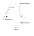
- FIG 1 (a) , (b) are exemplary diagrams showing a conventional PCB fixing structure.
- the PCB can be locked by a bending clip formed on the containing case.
- a screw can also be used to firmly fix the PCB onto the containing case, as shown in Figure 1 (b) .
- an apparatus for fixing a printed circuit board characterized by comprising:
- Figure 2 is an exemplary diagram showing the structure of a containing case 200, before assembly, for fixing a PCB 207 in accordance with an embodiment of the present invention.
- the containing case 200 comprises a bottom cover 201, a window member 203 and a top cover 205.
- a PCB 207 can be fixed and housed in the containing case 200.
- the bottom cover 201 is used to accommodate the PCB 207. As shown in Figure 2 , the bottom cover 201 comprises a bottom board portion 201a and a side wall portion 201b which is disposed upwards in a vertical direction at one edge of the bottom board portion 201a.
- the bottom board portion 201a can have a shape and size matched with the PCB 207 to receive the PCB 207 thereon.
- two clips 201c, 201e are provided at the edge of the board portion 201a opposite to the one where the side wall portion 201b is disposed to lock one side of the PCB 207 after assembly.
- the bottom board portion 201a is also provided with a pillar 201d which extends upwards in vertical direction. The position of the pillar 201d on the bottom board portion 201a should correspond to that of a opening 207a in the PCB 207 when the PCB 207 is placed on the bottom board portion 201a.
- the pillar 201d will penetrate through the opening 207a in the PCB 207 to hold the PCB 207 in position. It also acts as a guide to ensure correct placing of the PCB on the bottom part 201 of the case.
- the window member 203 has a shape matched with that of the side wall portion 201b of the bottom cover 201.
- the window member 203 is provided with two clips 203a, 203c at its top edge and two clips 203a', 203c' at its bottom edge that all project from the inner side of the front edge of the window member 203 in a direction so as to permit clipping of the window member 203 onto the bottom cover 201.
- the two clips 203a, 203c, 203a', 203c' can be clipped onto the side wall portion 201b, by which the window member 203 is detachably attached to the bottom cover 201.
- Two ribs 203b, 203d are integrally formed on the inner side of the window member 203, projecting in the same direction as that of the clips 203a, 203c, 203a', 203c'.
- the two ribs 203b, 203d protrude orthogonally from the window member 2003, extend downwardly and have a predetermined elasticity in that direction.
- the ribs 203b, 203d can be made of plastic to have the above said required elasticity.
- the position and extension length of the ribs 203b, 203d are set so that they can respectively penetrate through two openings 201 g, 201 h in the side wall portion 201b of the bottom cover 201.
- the top cover 205 can be attached to the bottom cover 201 after the window member 203 is attached to fix the PCB 207 in position, in order to further prevent the PCB 207 from damages by dust and other external influences.
- the PCB 207 is placed onto the bottom board portion 201a of the bottom cover 201 with the pillar 201d penetrating through the opening 207a of the PCB 207 for correctly positioning the PCB 207. Then, in the Figure 3(c) and 3(d) a slight push towards the bottom board portion 201a is applied onto the PCB 207 for locking the PCB 207 at one side with the clips 201c, 201e. After the above steps, the PCB 207 is put on the bottom board portion 201a with only one side locked by the clips 201c, 201e.
- the window member 203 is attached onto the bottom cover 201.
- the ribs 203b, 203d are made to penetrate respectively through corresponding openings 201 g, 201 h formed on the side wall portion 201b of the bottom cover 201.
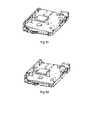
- Figure 4 is a perspective view showing the PCB 207 assembled in the containing case 200.
- the PCB 207 is locked at one side by the two clips 201c, 201e and elastically fixed at the other side with the two ribs 203b, 203d.
- top cover 205 can be assembled to the bottom cover 201 with the conventional means to further protect the PCB 207 from damages by outer forces.
- a PCB can be mounted in a containing case without using separate, mechanically distinct fastening components, such as screws and clips. Therefore, when the window member is assembled in position, the PCB will be automatically fixed by the ribs which are integrally formed on the window member, by which misoperation during the assembly procedure can be avoided. In addition, since the PCB is fixed at one side by the elastic ribs, impact or shock from outer environment can be partly absorbed, which will provide more protections for the electrics devices on the PCB from cracking under impact.
- the protruding elements of the window member 203 are formed as ribs 203b and 203d, such protruding elements may have other shapes as long as they exert downward pressure on the PCB when the window member 203 is mounted.
Landscapes
- Engineering & Computer Science (AREA)
- Microelectronics & Electronic Packaging (AREA)
- Casings For Electric Apparatus (AREA)
Abstract
An apparatus for fixing a printed circuit board is provided. The apparatus comprises a bottom member for accommodating the printed circuit board and an assembly member which can be detachably attached to the second part of the bottom member. The bottom member comprises a first part for the printed circuit board to be placed thereon, and a second part which is disposed upwards in a vertical direction at one edge of the first part and provided with at least one openings therein. The assembly member being integrally formed at the side towards the second part with at least one fixing member. When the assembly member is attached onto the second part of the bottom member, the fixing members will penetrate through the at least one openings of the second part to elastically fix the printed circuit board onto the first part of the bottom member.
Description
- The present invention relates to an apparatus for fixing a printed circuit board (PCB).
- The PCB is one of the important components of electronic equipments, which generally is fixed to a containing case of the electronic equipment by fastening screws or bending clips.
-
Figure 1 (a) ,(b) are exemplary diagrams showing a conventional PCB fixing structure. As shown inFigure 1(a) , the PCB can be locked by a bending clip formed on the containing case. A screw can also be used to firmly fix the PCB onto the containing case, as shown inFigure 1 (b) . - Such solution will cause a number of problems. For instance, a common disadvantage of the prior art structure is that the firmly-fixed PCB is not flexible enough when submitted to shocks, resulting in damage of the circuitry on the PCB.
- In addition, complicated or inconvenient assembly steps of the screws or clips are required, which will inevitably increase the cost and the possibilities of incorrect manipulation during the manufacture and assembly process. For example, a worker is likely to forget to fasten the screws or the screws may be lost during the assembly procedure.
- In view of the above-described problems, the present invention was developed.
- According to one aspect of the invention, there is provided an apparatus for fixing a printed circuit board, characterized by comprising:
- a bottom member for accommodating the printed circuit board, the bottom member having
a first part for the printed circuit board to be placed thereon, and
a second part which is disposed orthogonally to the first part and provided with at least one opening therein, - an assembly member which can be detachably attached to the second part of the bottom member, the assembly member being integrally formed at the side towards the second part with at least one fixing member,
- upon the attachment of the assembly member onto the second part of the bottom member, the fixing members being able to penetrate through said at least one opening of the second part to exert pressure on the printed circuit board towards the first part of the bottom member.
- These and other aspects, features and advantages of the present invention will become apparent from the following description in connection with the accompanying drawings in which:
-
Figure 1(a) ,(b) are exemplary diagrams showing a conventional PCB fixing structure with fastening screws and bending clips; -
Figure 2 is a perspective view showing the structure of a containing case, before assembled, for fixing a PCB in accordance with an embodiment of the present invention; -
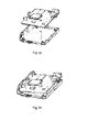
Figure 3 (a) to (f) are exemplary diagrams showing the procedure of fixing a PCB into the containing case in accordance with the embodiment of the present invention; and -
Figure 4 is a perspective view showing the PCB assembled in the containing case in accordance with the embodiment of the present invention. - In the following description, various aspects of an embodiment of the present invention will be described. For purposes of explanation, specific configurations and details are set forth in order to provide a thorough understanding. However, it will also be apparent to one skilled in the art that the present invention may be practiced without the specific details present herein.
-
Figure 2 is an exemplary diagram showing the structure of a containing case 200, before assembly, for fixing aPCB 207 in accordance with an embodiment of the present invention. - Referring to
Figure 2 , the containing case 200 comprises abottom cover 201, a window member 203 and a top cover 205. A PCB 207 can be fixed and housed in the containing case 200. - The
bottom cover 201 is used to accommodate the PCB 207. As shown inFigure 2 , thebottom cover 201 comprises a bottom board portion 201a and a side wall portion 201b which is disposed upwards in a vertical direction at one edge of the bottom board portion 201a. - The bottom board portion 201a can have a shape and size matched with the PCB 207 to receive the PCB 207 thereon. In this embodiment, two clips 201c, 201e are provided at the edge of the board portion 201a opposite to the one where the side wall portion 201b is disposed to lock one side of the PCB 207 after assembly. The bottom board portion 201a is also provided with a pillar 201d which extends upwards in vertical direction. The position of the pillar 201d on the bottom board portion 201a should correspond to that of a opening 207a in the PCB 207 when the PCB 207 is placed on the bottom board portion 201a. During assembly, when the
PCB 207 is placed on the bottom board portion 201a in a correction orientation, the pillar 201d will penetrate through the opening 207a in the PCB 207 to hold thePCB 207 in position. It also acts as a guide to ensure correct placing of the PCB on thebottom part 201 of the case. - As shown in
Figure 2 , the window member 203 has a shape matched with that of the side wall portion 201b of thebottom cover 201. In this embodiment, the window member 203 is provided with twoclips 203a, 203c at its top edge and two clips 203a', 203c' at its bottom edge that all project from the inner side of the front edge of the window member 203 in a direction so as to permit clipping of the window member 203 onto thebottom cover 201. As will described later, the twoclips 203a, 203c, 203a', 203c' can be clipped onto the side wall portion 201b, by which the window member 203 is detachably attached to thebottom cover 201. - Two
ribs 203b, 203d are integrally formed on the inner side of the window member 203, projecting in the same direction as that of theclips 203a, 203c, 203a', 203c'. The tworibs 203b, 203d protrude orthogonally from the window member 2003, extend downwardly and have a predetermined elasticity in that direction. Theribs 203b, 203d can be made of plastic to have the above said required elasticity. The position and extension length of theribs 203b, 203d are set so that they can respectively penetrate through two openings 201 g, 201 h in the side wall portion 201b of thebottom cover 201. By pressing with a downward component on the PCB once the window member is clipped into position on the side wall member, the ribs elastically fix thePCB 207 onto the bottom board portion 201a of thebottom cover 201. - The top cover 205 can be attached to the
bottom cover 201 after the window member 203 is attached to fix thePCB 207 in position, in order to further prevent thePCB 207 from damages by dust and other external influences. - Next, the procedure of fixing the
PCB 207 into the containing case 200 in accordance with an embodiment of the present invention will be described with reference to theFigure 3 . - To assemble the
PCB 207 into the containing case 200, as shown infigures 3(a) and 3(b) , the PCB 207 is placed onto the bottom board portion 201a of thebottom cover 201 with the pillar 201d penetrating through the opening 207a of thePCB 207 for correctly positioning thePCB 207. Then, in theFigure 3(c) and 3(d) a slight push towards the bottom board portion 201a is applied onto the PCB 207 for locking the PCB 207 at one side with the clips 201c, 201e. After the above steps, the PCB 207 is put on the bottom board portion 201a with only one side locked by the clips 201c, 201e. - Next, the window member 203 is attached onto the
bottom cover 201. As shown inFigure 3(e) , firstly theribs 203b, 203d are made to penetrate respectively through corresponding openings 201 g, 201 h formed on the side wall portion 201b of thebottom cover 201. Then, as illustrated inFigure 3(f) , a slight force in the assembling direction is applied on the window member 203 to force on the side wall portion 201b, so that the twoclips 203a, 203c at the top edge and two clips 203a', 203c' at the bottom edge of the window member 203 are clipped respectively onto the top and bottom edge of the side wall portion 201b of thebottom cover 201 and the tworibs 203b, 203d elastically fix the other side of thePCB 207 onto thebottom cover 201. At this time, the PCB 207 is securely fixed to the containing case 200, with its one side locked by the clips 201c, 201e and the other side elastically fixed by theribs 203b, 203d. -
Figure 4 is a perspective view showing the PCB 207 assembled in the containing case 200. - As clearly shown in
Figure 4 , the PCB 207 is locked at one side by the two clips 201c, 201e and elastically fixed at the other side with the tworibs 203b, 203d. - It should be appreciated that, although not shown in
Figures 3 and4 , the top cover 205 can be assembled to thebottom cover 201 with the conventional means to further protect thePCB 207 from damages by outer forces. - As with the embodiment described above, a PCB can be mounted in a containing case without using separate, mechanically distinct fastening components, such as screws and clips. Therefore, when the window member is assembled in position, the PCB will be automatically fixed by the ribs which are integrally formed on the window member, by which misoperation during the assembly procedure can be avoided. In addition, since the PCB is fixed at one side by the elastic ribs, impact or shock from outer environment can be partly absorbed, which will provide more protections for the electrics devices on the PCB from cracking under impact.
- From the foregoing description, it will be evident for a person skilled in the art that numerous modifications may be made to the illustrative embodiments and that other arrangements may be devised without departing from the spirit and scope of the present invention as defined by the appended claims. In particular, while in the above embodiment, the protruding elements of the window member 203 are formed as
ribs 203b and 203d, such protruding elements may have other shapes as long as they exert downward pressure on the PCB when the window member 203 is mounted.
Claims (8)
- An apparatus (200) for fixing a printed circuit board (207), characterized by comprising:a bottom member (201) for accommodating the printed circuit board (207), the bottom member (201) having
a first part (201a) for the printed circuit board (207) to be placed thereon, and
a second part (201b) which is disposed orthogonally to the first part (201a) and provided with at least one opening (201 g, 201 h) therein,an assembly member (203) which can be detachably attached to the second part (201b) of the bottom member (201), the assembly member (203) being integrally formed at the side towards the second part (201b) with at least one fixing member (203b, 203d),upon the attachment of the assembly member (203) onto the second part (201b) of the bottom member (201), the fixing members (203b, 203d) being able to penetrate through said at least one opening (201 g, 201 h) of the second part (201b) to exert pressure on the printed circuit board (207) towards the first part (201a) of the bottom member (201). - The apparatus according to claim 1, wherein the fixing member (203b) is a rib made of plastic to have elasticity in the direction of fixing the printed circuit board (207) onto the first part (201a) for the printed circuit board (207).
- The apparatus according to claim 1, wherein the assembly member (203) has a shape matched with that of the second part (201b) of the bottom member (201).
- The apparatus according to claim 3, wherein the assembly member (203) is provided with at leas two clips (203a, 203c, 203a', 203c') respectively formed at its top and bottom edges that can be clipped onto the second part (201b) of the bottom member (201).
- The apparatus according to claim 1, wherein the first part (201a) of the bottom member (201) has a shape matched with that of the printed circuit board (207) to be placed thereon.
- The apparatus according to claim 5, wherein the first part (201a) of the bottom member (201) is provided with a pillar (201d) which extends upwards in vertical direction at a position corresponding to that of a opening (207a) in the printed circuit board (207) when the printed circuit board (207) is placed on the first part (201a).
- The apparatus according to claim 5, wherein the first part (201a) of the bottom member (201) is provided with at least one clips (201c, 201e) at the edge opposite to the one where the second part (201b) is disposed to lock one side of the printed circuit board (207) after assembled.
- The apparatus according to claim 1, further comprising a top member (205) that can be assembled to the bottom member (201) to further protect the PCB 207 from damages by outer forces.
Priority Applications (1)
| Application Number | Priority Date | Filing Date | Title |
|---|---|---|---|
| EP10165475A EP2568786A1 (en) | 2010-06-10 | 2010-06-10 | Apparatus for fixing a printed circuit board |
Applications Claiming Priority (1)
| Application Number | Priority Date | Filing Date | Title |
|---|---|---|---|
| EP10165475A EP2568786A1 (en) | 2010-06-10 | 2010-06-10 | Apparatus for fixing a printed circuit board |
Publications (1)
| Publication Number | Publication Date |
|---|---|
| EP2568786A1 true EP2568786A1 (en) | 2013-03-13 |
Family
ID=47008207
Family Applications (1)
| Application Number | Title | Priority Date | Filing Date |
|---|---|---|---|
| EP10165475A Withdrawn EP2568786A1 (en) | 2010-06-10 | 2010-06-10 | Apparatus for fixing a printed circuit board |
Country Status (1)
| Country | Link |
|---|---|
| EP (1) | EP2568786A1 (en) |
Citations (3)
| Publication number | Priority date | Publication date | Assignee | Title |
|---|---|---|---|---|
| DE8912800U1 (en) * | 1989-10-28 | 1991-02-21 | Philips Patentverwaltung Gmbh, 2000 Hamburg | PCB housing |
| EP0590609A1 (en) * | 1992-09-28 | 1994-04-06 | Hitachi Telecom Technologies, Ltd. | Electric appliance, its assembling method, and its housing structure |
| US20030031004A1 (en) * | 2001-08-10 | 2003-02-13 | Paul Hooper | Screwless circuit board attachment |
-
2010
- 2010-06-10 EP EP10165475A patent/EP2568786A1/en not_active Withdrawn
Patent Citations (3)
| Publication number | Priority date | Publication date | Assignee | Title |
|---|---|---|---|---|
| DE8912800U1 (en) * | 1989-10-28 | 1991-02-21 | Philips Patentverwaltung Gmbh, 2000 Hamburg | PCB housing |
| EP0590609A1 (en) * | 1992-09-28 | 1994-04-06 | Hitachi Telecom Technologies, Ltd. | Electric appliance, its assembling method, and its housing structure |
| US20030031004A1 (en) * | 2001-08-10 | 2003-02-13 | Paul Hooper | Screwless circuit board attachment |
Similar Documents
| Publication | Publication Date | Title |
|---|---|---|
| JPH0530381Y2 (en) | ||
| JP5759914B2 (en) | Electronic control unit | |
| US20150337882A1 (en) | Clip attachment structure | |
| EP2665131A2 (en) | Attachment structure of an electronic device | |
| CN102356243A (en) | Structure for fastening resin part | |
| US8100710B1 (en) | Flash drive mounting apparatus having a base with a plurality of openings and two fixing members with hook-and-loop fasteners | |
| EP2659753B1 (en) | Grounding structure for printed circuit board | |
| EP1220592A1 (en) | An apparatus and a method of providing a flexible electrical connection between two components | |
| JP4690224B2 (en) | Circuit board | |
| KR101375109B1 (en) | Nut fixing device | |
| CN109327982B (en) | Electronic device housing and electronic device having the same | |
| KR101559932B1 (en) | Antenna holder for vehicle comprising cable protection part | |
| US8902610B2 (en) | Electronic device | |
| KR101388758B1 (en) | Coupling device for shielding type shield can | |
| JP2008258497A (en) | Flexible substrate fixing structure | |
| WO2022190812A1 (en) | Electronic device | |
| JP2570466Y2 (en) | Clip for wire harness | |
| JPH0341506Y2 (en) | ||
| JP3268617B2 (en) | Keypad holding structure in portable radio communication equipment | |
| CN117090805A (en) | Component installation structure and component installation method | |
| JPS6316174Y2 (en) | ||
| JPH0510467Y2 (en) | ||
| JPH0629187U (en) | Cable stop structure | |
| JP2008277493A (en) | Flexible substrate fixing structure | |
| JP2009299708A (en) | Two-piece clip |
Legal Events
| Date | Code | Title | Description |
|---|---|---|---|
| PUAI | Public reference made under article 153(3) epc to a published international application that has entered the european phase |
Free format text: ORIGINAL CODE: 0009012 |
|
| AK | Designated contracting states |
Kind code of ref document: A1 Designated state(s): AL AT BE BG CH CY CZ DE DK EE ES FI FR GB GR HR HU IE IS IT LI LT LU LV MC MK MT NL NO PL PT RO SE SI SK SM TR |
|
| AX | Request for extension of the european patent |
Extension state: BA ME RS |
|
| STAA | Information on the status of an ep patent application or granted ep patent |
Free format text: STATUS: THE APPLICATION IS DEEMED TO BE WITHDRAWN |
|
| 18D | Application deemed to be withdrawn |
Effective date: 20130914 |