EP2568530A1 - Mobile wireless communications device including a slot antenna and related methods - Google Patents
Mobile wireless communications device including a slot antenna and related methods Download PDFInfo
- Publication number
- EP2568530A1 EP2568530A1 EP11180792A EP11180792A EP2568530A1 EP 2568530 A1 EP2568530 A1 EP 2568530A1 EP 11180792 A EP11180792 A EP 11180792A EP 11180792 A EP11180792 A EP 11180792A EP 2568530 A1 EP2568530 A1 EP 2568530A1
- Authority
- EP
- European Patent Office
- Prior art keywords
- slot
- wireless communications
- mobile wireless
- pcb
- communications device
- Prior art date
- Legal status (The legal status is an assumption and is not a legal conclusion. Google has not performed a legal analysis and makes no representation as to the accuracy of the status listed.)
- Granted
Links
Images




Classifications
-
- H—ELECTRICITY
- H01—ELECTRIC ELEMENTS
- H01Q—ANTENNAS, i.e. RADIO AERIALS
- H01Q1/00—Details of, or arrangements associated with, antennas
- H01Q1/12—Supports; Mounting means
- H01Q1/22—Supports; Mounting means by structural association with other equipment or articles
- H01Q1/24—Supports; Mounting means by structural association with other equipment or articles with receiving set
- H01Q1/241—Supports; Mounting means by structural association with other equipment or articles with receiving set used in mobile communications, e.g. GSM
- H01Q1/242—Supports; Mounting means by structural association with other equipment or articles with receiving set used in mobile communications, e.g. GSM specially adapted for hand-held use
- H01Q1/243—Supports; Mounting means by structural association with other equipment or articles with receiving set used in mobile communications, e.g. GSM specially adapted for hand-held use with built-in antennas
-
- H—ELECTRICITY
- H01—ELECTRIC ELEMENTS
- H01Q—ANTENNAS, i.e. RADIO AERIALS
- H01Q1/00—Details of, or arrangements associated with, antennas
- H01Q1/36—Structural form of radiating elements, e.g. cone, spiral, umbrella; Particular materials used therewith
- H01Q1/38—Structural form of radiating elements, e.g. cone, spiral, umbrella; Particular materials used therewith formed by a conductive layer on an insulating support
-
- H—ELECTRICITY
- H01—ELECTRIC ELEMENTS
- H01Q—ANTENNAS, i.e. RADIO AERIALS
- H01Q1/00—Details of, or arrangements associated with, antennas
- H01Q1/52—Means for reducing coupling between antennas; Means for reducing coupling between an antenna and another structure
- H01Q1/526—Electromagnetic shields
-
- H—ELECTRICITY
- H01—ELECTRIC ELEMENTS
- H01Q—ANTENNAS, i.e. RADIO AERIALS
- H01Q13/00—Waveguide horns or mouths; Slot antennas; Leaky-waveguide antennas; Equivalent structures causing radiation along the transmission path of a guided wave
- H01Q13/10—Resonant slot antennas
- H01Q13/106—Microstrip slot antennas
Definitions
- the present disclosure generally relates to the field of wireless communications systems, and, more particularly, to mobile wireless communications devices and related methods.
- cellular telephones allow users to place and receive voice calls almost anywhere they travel.
- cellular telephone technology has increased, so too has the functionality of cellular devices and the different types of devices available to users.
- PDA personal digital assistant
- multi-function devices may also allow users to wirelessly send and receive electronic mail (email) messages and access the Internet via a cellular network and/or a wireless local area network (WLAN), for example.
- email electronic mail
- WLAN wireless local area network
- FIG. 1 is a top plan view of a mobile wireless communications device including an electrically conductive enclosure having a slot therein defining a slot antenna in accordance with one example embodiment.
- FIG. 2 is a schematic block diagram of a portion of the device of FIG. 1 .
- FIG. 3 is a side schematic view of the portion of the device in FIG. 2 .
- FIG. 4 is a perspective view of a portion of a device including an antenna feed in accordance with another example embodiment.
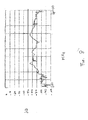
- FIG. 5 is a graph of measured return loss for a prototype mobile wireless communications device without a tuning element.
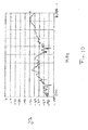
- FIG. 6 is a graph of measured gain for the prototype mobile wireless communications device without a tuning element.
- FIG. 7 is a graph of measured return loss for a prototype mobile wireless communications device with a FR-4 tuning element.
- FIG. 8 is a graph of measured gain for the prototype mobile wireless communications device with the FR-4 tuning element.
- FIG. 9 is a graph of measured return loss for a prototype mobile wireless communications device with a TDK ceramic tuning element.
- FIG. 10 is a graph of measured gain for the prototype mobile wireless communications device with the TDK ceramic tuning element.
- FIG. 11 is a schematic block diagram illustrating additional components that may be included in the mobile wireless communications device of FIG. 1 .
- a mobile wireless communications device may include a portable housing and a printed circuit board (PCB) carried by the portable housing.
- the mobile wireless communications device may also include at least one electronic component carried by the PCB and an electrically conductive enclosure coupled to the PCB and having a top spaced above the PCB over the at least one electronic component.
- the top of the electrically conductive enclosure may have a slot therein defining a slot antenna.
- the mobile wireless communications device may further include a tuning element carried by the electrically conductive enclosure and being positioned over the slot, for example.
- the tuning element may include a dielectric material body.
- the tuning element may further include a conductive material layer on the dielectric material body, for example.
- the slot may include a base slot, and first and second parallel slots extending in opposite directions from the base slot.
- the base slot may have opposing ends, and the first and second parallel slots may extend from the opposing ends, for example.
- the electrically conductive enclosure may further include a sidewall depending from the top, for example.
- the mobile wireless communications device may further include at least one antenna feed carried by the PCB and coupled to the electrically conductive enclosure adjacent the slot.
- the at least one antenna feed may include a pair of antenna feeds coupled to the electrically conductive enclosure on opposing sides of the slot, for example.
- the at least one antenna feed may include at least one of a flexible stripline and a spring contact.
- the mobile wireless communications device of may further include a conductive layer carried by the PCB defining a ground plane, for example.
- the electrically conductive enclosure is carried above the ground plane.
- a method aspect is directed to a method of making a mobile wireless communications device that may include a portable housing, a printed circuit board (PCB) carried by the portable housing, and at least one electronic component carried by the PCB.
- the method may include forming a slot in a top of an electrically conductive enclosure to be coupled to the PCB to form a slot antenna.
- the top may be spaced above the PCB over the at least one electronic component.
- a mobile wireless communications device 30 illustratively includes a portable housing 31 a printed circuit board (PCB) 32 , carried by the portable housing.
- the PCB 32 also includes a conductive layer 46 defining a ground plane ( FIG. 3 ).
- the exemplary device 30 further illustratively includes a display 60 and a plurality of control keys including an "off hook” (i.e., initiate phone call) key 61 , an "on hook” (i.e., discontinue phone call) key 62 , a menu key 63 , and a return or escape key 64 . Operation of the various device components and input keys, etc., will be described further below with reference to FIG. 11 .
- the wireless communications device 30 also includes electronic components 33a-33n carried by PCB 32 .
- the electronic components 33a-33n may include wireless communications circuitry configured to perform a wireless communications function, for example, wireless voice or data communications.
- Other circuitry, for example, discrete components, associated with the mobile wireless communications device 30 may also be carried by the PCB 32.
- An electrically conductive enclosure 34 is coupled to the PCB 32 and carried above the ground plane 46 .
- the electrically conductive enclosure 34 includes a top 47 spaced above PCB 32 over the electronic components 33a-33n .
- the electrically conductive enclosure 34 also includes a sidewall 37 depending from the top 47 .
- the top 47 of the electrically conductive enclosure 34 has a slot 35 therein defining a slot antenna.
- the slot 35 illustratively includes a base slot 36 having opposing ends 41 , 42 .
- First and second parallel slots 43 , 44 extend in opposite directions from the opposing ends 41 , 42 of the base slot 36 .
- the slot 35 may extend in other directions, but it may be desirable that the slot does not "double over" on itself as this may reduce antenna efficiency and thus performance.
- the electrically conductive enclosure 34 may have additional slots or openings for ventilation, which may be relatively small compared to the slot 35 .
- the electrically conductive enclosure 34 may have more than one slot therein defining more than one slot antenna.
- the length of the slot 35 determines the operating frequency of the slot antenna.
- the position of the electrically conductive enclosure 34 with respect to the ground plane 46 is another variable that may affect performance of the slot antenna.
- the slot 35 be the correct length, the electrically conductive enclosure 34 surrounding the slot 35 is large enough to support circulating currents around the slot, and the cavity, i.e. the distance of the slot and the electrically conductive enclosure 34 above the PCB 32 , has sufficient depth. Physical restraints of the mechanics of the mobile wireless communications device 30 may hamper obtaining of desired characteristics.
- the mobile wireless communications device 30 includes a tuning element 50 carried by the electrically conductive enclosure 34 .
- the tuning member 50 loads the slot 35 as a parasitic element.
- the tuning element 50 is illustratively positioned over the slot 35 , and more particularly, bridges or spans the slot 35 .
- the tuning member 50 includes a dielectric material body 51 and may have a relatively high dielectric constant, for example.
- the dielectric material body 51 may be FR-4 dielectric material or a ceramic material.
- the dielectric material body 51 may include other dielectric materials.
- the tuning element 50 may also optionally include a conductive material layer 52 on the dielectric material body 51 .
- the conductive material layer 52 may be copper, for example.
- the conductive material layer 52 may be another conductive material, as will be appreciated by those skilled in the art. More than one tuning element may be used, as will be appreciated by those skilled in the art.
- the thickness of the tuning element 50 may be particularly useful for determining gain and return loss of the slot antenna.
- the height of the slot 35 and the tuning element 50 above the PCB 32 also determines the gain or return loss.
- the thickness of the tuning element 50 and the height of the tuning element and the slot 35 above the PCB may be the primary adjustments for determining gain or return loss.
- the position of the electrically conductive enclosure 34 in the X-Y plane on the ground plane 46 , and the X-Y position of the tuning element 50 may also determine the gain or return loss of the slot antenna.
- the height of the tuning element 50 and the electrically conductive enclosure 34 may be adjustable via an adjustment mechanism. This may accommodate in-situ adjustment and thus, different gain patterns, for example.
- the slot antenna may be particularly useful for operating in the IEEE 802.11a frequency band of approximately 5.2 GHz to 5.8 GHz.
- mounting a slot antenna on the electrically conductive enclosure 34 advantageously helps ease the problem of finding the room or space within the portable housing 31 .
- the IEEE 802.11a standard describes a single band antenna, moving it away from a clear area onto the PCB, for example, may be particularly useful as it would leave more room for multi-band antennas, which are typically more difficult to implement.
- a pair of antenna feeds in the form of spring contacts 53a, 53b are carried by the PCB 32 and coupled to the electrically conductive enclosure 34 adjacent the slot 35 , and more particularly, on opposing sides of the slot.
- the location where the pair of spring contacts 53a, 53b coupled to the electrically conductive enclosure 34 adjacent the slot 35 determines multiple resonances, as will be appreciated by those skilled in the art.
- one resonance may be obtained by coupling the pair of spring contacts 53a , 53b adjacent the center of the slot 35 with respect to its length. If the pair of spring contacts 53a, 53b are coupled off-center of the slot with respect to its length, multiple resonance may be obtained.
- the antenna feeds are in the form of flexible striplines 53a ⁇ , 53b ⁇ .
- the flexible striplines 53a ⁇ 53b' are illustratively bent over in a c-shape.
- An outer portion of one of the flexible striplines 53a ⁇ is trimmed back to expose a center portion 55 ⁇ .
- the center portion 55 ⁇ couples to the electrically conductive enclosure 34 ⁇ adjacent the slot 35' and crosses over the slot.
- the second flexible stripline 53b ⁇ couples to the ground plane 46 ⁇ .
- the second flexible stripline 53b ⁇ is 53mm away from the first flexible stripline 53a ⁇ .
- the second flexible stripline 53b ⁇ does not cross the slot 35 ⁇ , but rather couples to the electrically conductive enclosure 34 ⁇ .
- the pair of antenna feeds 53a ⁇ , 53b' may be another type of feed, for example, pogo pins, or other mechanical structure and may be coupled in another arrangement, as will be appreciated by those skilled in the art.
- FIGS. 5-6 a measured return loss graph and an antenna gain graph for a prototype mobile wireless communications device similar to that described above with respect to FIG. 1 , but without a tuning element are respectively illustrated.
- FIGS. 7-8 a measured return loss graph and antenna gain graph for the prototype mobile wireless communications device including a tuning element are respectively illustrated.
- the tuning element was a FR-4 dielectric material strip that measured 9 mm x 3 mm by 4 mm and was positioned in the center of the slot with respect to it length and width. A layer of copper was carried by the FR-4.
- the tuning element was a TDK ceramic dielectric material that measured 30 mm x 8 mm by 1 mm and was positioned equally over the slot with respect to it length and width.
- the TDK ceramic dielectric material had a dielectric constant of 6.2.
- a method aspect is directed to a method of making a mobile wireless communications device 30 that includes a portable housing 31 , a printed circuit board 32 (PCB) carried by the portable housing, and electronic components 33a-33n carried by the PCB.
- the method also includes forming a slot 35 in a top 47 of an electrically conductive enclosure 34 to be coupled to the PCB 32 to form a slot antenna.
- the top 47 is to be spaced above the PCB 32 over the electronic components 33a-33n .
- the device 1000 illustratively includes a housing 1200 , a keyboard or keypad 1400 and an output device 1600 .
- the output device shown is a display 1600 , which may comprise a full graphic LCD. Other types of output devices may alternatively be utilized.
- a processing device 1800 is contained within the housing 1200 and is coupled between the keypad 1400 and the display 1600 . The processing device 1800 controls the operation of the display 1600 , as well as the overall operation of the mobile device 1000 , in response to actuation of keys on the keypad 1400 .
- the housing 1200 may be elongated vertically, or may take on other sizes and shapes (including clamshell housing structures).
- the keypad may include a mode selection key, or other hardware or software for switching between text entry and telephony entry.
- FIG. 11 In addition to the processing device 1800 , other parts of the mobile device 1000 are shown schematically in FIG. 11 . These include a communications subsystem 1001 ; a short-range communications subsystem 1020 ; the keypad 1400 and the display 1600 , along with other input/output devices 1060 , 1080 , 1100 and 1120 ; as well as memory devices 1160 , 1180 and various other device subsystems 1201 .
- the mobile device 1000 may comprise a two-way RF communications device having data and, optionally, voice communications capabilities. In addition, the mobile device 1000 may have the capability to communicate with other computer systems via the Internet.
- Operating system software executed by the processing device 1800 is stored in a persistent store, such as the flash memory 1160 , but may be stored in other types of memory devices, such as a read only memory (ROM) or similar storage element.
- system software, specific device applications, or parts thereof may be temporarily loaded into a volatile store, such as the random access memory (RAM) 1180 .
- Communications signals received by the mobile device may also be stored in the RAM 1180 .
- the processing device 1800 in addition to its operating system functions, enables execution of software applications 1300A-1300N on the device 1000 .
- a personal information manager (PIM) application may be installed during manufacture.
- the PIM may be capable of organizing and managing data items, such as e-mail, calendar events, voice mails, appointments, and task items.
- the PIM application may also be capable of sending and receiving data items via a wireless network 1401 .
- the PIM data items may be seamlessly integrated, synchronized and updated via the wireless network 1401 with corresponding data items stored or associated with a host computer system.
- the communications subsystem 1001 includes a receiver 1500 , a transmitter 1520, and one or more antennas 1540 and 1560 .
- the communications subsystem 1001 also includes a processing module, such as a digital signal processor (DSP) 1580 , and local oscillators (LOs) 1601 .
- DSP digital signal processor
- LOs local oscillators
- a mobile device 1000 may include a communications subsystem 1001 designed to operate with the MobitexTM, Data TACTM or General Packet Radio Service (GPRS) mobile data communications networks, and also designed to operate with any of a variety of voice communications networks, such as AMPS, TDMA, CDMA, WCDMA, PCS, GSM, EDGE, etc. Other types of data and voice networks, both separate and integrated, may also be utilized with the mobile device 1000 .
- the mobile device 1000 may also be compliant with other communications standards such as 3GSM, 3GPP, UMTS, 4G, etc.
- Network access requirements vary depending upon the type of communication system. For example, in the Mobitex and DataTAC networks, mobile devices are registered on the network using a unique personal identification number or PIN associated with each device. In GPRS networks, however, network access is associated with a subscriber or user of a device. A GPRS device therefore typically involves use of a subscriber identity module, commonly referred to as a SIM card, in order to operate on a GPRS network.
- SIM card subscriber identity module
- the mobile device 1000 may send and receive communications signals over the communication network 1401 .
- Signals received from the communications network 1401 by the antenna 1540 are routed to the receiver 1500 , which provides for signal amplification, frequency down conversion, filtering, channel selection, etc., and may also provide analog to digital conversion. Analog-to-digital conversion of the received signal allows the DSP 1580 to perform more complex communications functions, such as demodulation and decoding.
- signals to be transmitted to the network 1401 are processed (e.g. modulated and encoded) by the DSP 1580 and are then provided to the transmitter 1520 for digital to analog conversion, frequency up conversion, filtering, amplification and transmission to the communication network 1401 (or networks) via the antenna 1560 .
- the DSP 1580 provides for control of the receiver 1500 and the transmitter 1520 .
- gains applied to communications signals in the receiver 1500 and transmitter 1520 may be adaptively controlled through automatic gain control algorithms implemented in the DSP 1580 .
- a received signal such as a text message or web page download
- the communications subsystem 1001 is input to the processing device 1800 .
- the received signal is then further processed by the processing device 1800 for an output to the display 1600 , or alternatively to some other auxiliary I/O device 1060 .
- a device may also be used to compose data items, such as e-mail messages, using the keypad 1400 and/or some other auxiliary I/O device 1060 , such as a touchpad, a rocker switch, a thumb-wheel, or some other type of input device.
- the composed data items may then be transmitted over the communications network 1401 via the communications subsystem 1001 .
- a voice communications mode In a voice communications mode, overall operation of the device is substantially similar to the data communications mode, except that received signals are output to a speaker 1100 , and signals for transmission are generated by a microphone 1120 .
- Alternative voice or audio I/O subsystems such as a voice message recording subsystem, may also be implemented on the device 1000 .
- the display 1600 may also be utilized in voice communications mode, for example to display the identity of a calling party, the duration of a voice call, or other voice call related information.
- the short-range communications subsystem enables communication between the mobile device 1000 and other proximate systems or devices, which need not necessarily be similar devices.
- the short-range communications subsystem may include an infrared device and associated circuits and components, a BluetoothTM communications module to provide for communication with similarly-enabled systems and devices, or a near field communications (NFC) sensor for communicating with a NFC device or NFC tag via NFC communications.
- NFC near field communications
Landscapes
- Physics & Mathematics (AREA)
- Electromagnetism (AREA)
- Engineering & Computer Science (AREA)
- Computer Networks & Wireless Communication (AREA)
- Support Of Aerials (AREA)
- Waveguide Aerials (AREA)
- Transceivers (AREA)
- Mobile Radio Communication Systems (AREA)
Abstract
Description
- The present disclosure generally relates to the field of wireless communications systems, and, more particularly, to mobile wireless communications devices and related methods.
- Mobile wireless communications systems continue to grow in popularity and have become an integral part of both personal and business communications. For example, cellular telephones allow users to place and receive voice calls almost anywhere they travel. Moreover, as cellular telephone technology has increased, so too has the functionality of cellular devices and the different types of devices available to users. For example, many cellular devices now incorporate personal digital assistant (PDA) features such as calendars, address books, task lists, etc. Moreover, such multi-function devices may also allow users to wirelessly send and receive electronic mail (email) messages and access the Internet via a cellular network and/or a wireless local area network (WLAN), for example.
- Even so, as the functionality of cellular communications devices continues to increase, so too does the demand for smaller devices which are easier and more convenient for users to carry. One challenge this poses for cellular device manufacturers is designing housings that cooperate with antennas to provide desired operating characteristics within the relatively limited amount of space available.
-
FIG. 1 is a top plan view of a mobile wireless communications device including an electrically conductive enclosure having a slot therein defining a slot antenna in accordance with one example embodiment. -
FIG. 2 is a schematic block diagram of a portion of the device ofFIG. 1 . -
FIG. 3 is a side schematic view of the portion of the device inFIG. 2 . -
FIG. 4 is a perspective view of a portion of a device including an antenna feed in accordance with another example embodiment. -
FIG. 5 is a graph of measured return loss for a prototype mobile wireless communications device without a tuning element. -
FIG. 6 is a graph of measured gain for the prototype mobile wireless communications device without a tuning element. -
FIG. 7 is a graph of measured return loss for a prototype mobile wireless communications device with a FR-4 tuning element. -
FIG. 8 is a graph of measured gain for the prototype mobile wireless communications device with the FR-4 tuning element. -
FIG. 9 is a graph of measured return loss for a prototype mobile wireless communications device with a TDK ceramic tuning element. -
FIG. 10 is a graph of measured gain for the prototype mobile wireless communications device with the TDK ceramic tuning element. -
FIG. 11 is a schematic block diagram illustrating additional components that may be included in the mobile wireless communications device ofFIG. 1 . - The present invention will now be described more fully hereinafter with reference to the accompanying drawings, in which preferred embodiments of the invention are shown. This invention may, however, be embodied in many different forms and should not be construed as limited to the embodiments set forth herein. Rather, these embodiments are provided so that this disclosure will be thorough and complete, and will fully convey the scope of the invention to those skilled in the art. Like numbers refer to like elements throughout, and prime notation is used to indicate similar elements or steps in alternative embodiments.
- In accordance with one exemplary aspect, a mobile wireless communications device may include a portable housing and a printed circuit board (PCB) carried by the portable housing. The mobile wireless communications device may also include at least one electronic component carried by the PCB and an electrically conductive enclosure coupled to the PCB and having a top spaced above the PCB over the at least one electronic component. The top of the electrically conductive enclosure may have a slot therein defining a slot antenna.
- The mobile wireless communications device may further include a tuning element carried by the electrically conductive enclosure and being positioned over the slot, for example. The tuning element may include a dielectric material body. The tuning element may further include a conductive material layer on the dielectric material body, for example.
- The slot may include a base slot, and first and second parallel slots extending in opposite directions from the base slot. The base slot may have opposing ends, and the first and second parallel slots may extend from the opposing ends, for example.
- The electrically conductive enclosure may further include a sidewall depending from the top, for example. The mobile wireless communications device may further include at least one antenna feed carried by the PCB and coupled to the electrically conductive enclosure adjacent the slot. The at least one antenna feed may include a pair of antenna feeds coupled to the electrically conductive enclosure on opposing sides of the slot, for example. The at least one antenna feed may include at least one of a flexible stripline and a spring contact.
- The mobile wireless communications device of may further include a conductive layer carried by the PCB defining a ground plane, for example. The electrically conductive enclosure is carried above the ground plane.
- A method aspect is directed to a method of making a mobile wireless communications device that may include a portable housing, a printed circuit board (PCB) carried by the portable housing, and at least one electronic component carried by the PCB. The method may include forming a slot in a top of an electrically conductive enclosure to be coupled to the PCB to form a slot antenna. The top may be spaced above the PCB over the at least one electronic component.
- Referring initially to
FIGS. 1-3 , a mobilewireless communications device 30 illustratively includes a portable housing 31 a printed circuit board (PCB) 32, carried by the portable housing. ThePCB 32 also includes aconductive layer 46 defining a ground plane (FIG. 3 ). - The
exemplary device 30 further illustratively includes adisplay 60 and a plurality of control keys including an "off hook" (i.e., initiate phone call)key 61, an "on hook" (i.e., discontinue phone call)key 62, amenu key 63, and a return orescape key 64. Operation of the various device components and input keys, etc., will be described further below with reference toFIG. 11 . - The
wireless communications device 30 also includeselectronic components 33a-33n carried by PCB 32. Theelectronic components 33a-33n may include wireless communications circuitry configured to perform a wireless communications function, for example, wireless voice or data communications. Other circuitry, for example, discrete components, associated with the mobilewireless communications device 30 may also be carried by the PCB 32. - An electrically
conductive enclosure 34 is coupled to thePCB 32 and carried above theground plane 46. The electricallyconductive enclosure 34 includes a top 47 spaced abovePCB 32 over theelectronic components 33a-33n. The electricallyconductive enclosure 34 also includes asidewall 37 depending from thetop 47. - The
top 47 of the electricallyconductive enclosure 34 has aslot 35 therein defining a slot antenna. Theslot 35 illustratively includes abase slot 36 havingopposing ends 41, 42. First and secondparallel slots 43, 44 extend in opposite directions from theopposing ends 41, 42 of thebase slot 36. Theslot 35 may extend in other directions, but it may be desirable that the slot does not "double over" on itself as this may reduce antenna efficiency and thus performance. The electricallyconductive enclosure 34 may have additional slots or openings for ventilation, which may be relatively small compared to theslot 35. Moreover, the electricallyconductive enclosure 34 may have more than one slot therein defining more than one slot antenna. - The length of the
slot 35 determines the operating frequency of the slot antenna. The position of the electricallyconductive enclosure 34 with respect to theground plane 46 is another variable that may affect performance of the slot antenna. - For the slot antenna to operate in the correct mode for the frequency of operation and to give the desired bandwidth, it is desirable that the
slot 35 be the correct length, the electricallyconductive enclosure 34 surrounding theslot 35 is large enough to support circulating currents around the slot, and the cavity, i.e. the distance of the slot and the electricallyconductive enclosure 34 above thePCB 32, has sufficient depth. Physical restraints of the mechanics of the mobilewireless communications device 30 may hamper obtaining of desired characteristics. - To compensate for the increased difficulty of obtaining desired characteristics because of the physical constraints, i.e. size, the mobile
wireless communications device 30 includes atuning element 50 carried by the electricallyconductive enclosure 34. The tuningmember 50 loads theslot 35 as a parasitic element. Thetuning element 50 is illustratively positioned over theslot 35, and more particularly, bridges or spans theslot 35. The tuningmember 50 includes a dielectric material body 51 and may have a relatively high dielectric constant, for example. For example, the dielectric material body 51 may be FR-4 dielectric material or a ceramic material. Of course, the dielectric material body 51 may include other dielectric materials. - The
tuning element 50 may also optionally include a conductive material layer 52 on the dielectric material body 51. The conductive material layer 52 may be copper, for example. The conductive material layer 52 may be another conductive material, as will be appreciated by those skilled in the art. More than one tuning element may be used, as will be appreciated by those skilled in the art. - The thickness of the
tuning element 50 may be particularly useful for determining gain and return loss of the slot antenna. The height of theslot 35 and thetuning element 50 above thePCB 32 also determines the gain or return loss. The thickness of thetuning element 50 and the height of the tuning element and theslot 35 above the PCB may be the primary adjustments for determining gain or return loss. The position of the electricallyconductive enclosure 34 in the X-Y plane on theground plane 46, and the X-Y position of thetuning element 50 may also determine the gain or return loss of the slot antenna. As will be appreciated by those skilled in the art, the height of thetuning element 50 and the electricallyconductive enclosure 34 may be adjustable via an adjustment mechanism. This may accommodate in-situ adjustment and thus, different gain patterns, for example. - The slot antenna may be particularly useful for operating in the IEEE 802.11a frequency band of approximately 5.2 GHz to 5.8 GHz. As will be appreciated by those skilled in the art, mounting a slot antenna on the electrically
conductive enclosure 34 advantageously helps ease the problem of finding the room or space within theportable housing 31. As the IEEE 802.11a standard describes a single band antenna, moving it away from a clear area onto the PCB, for example, may be particularly useful as it would leave more room for multi-band antennas, which are typically more difficult to implement. - A pair of antenna feeds in the form of
spring contacts 53a, 53b are carried by thePCB 32 and coupled to the electricallyconductive enclosure 34 adjacent theslot 35, and more particularly, on opposing sides of the slot. - The location where the pair of
spring contacts 53a, 53b coupled to the electricallyconductive enclosure 34 adjacent theslot 35 determines multiple resonances, as will be appreciated by those skilled in the art. In particular, one resonance may be obtained by coupling the pair ofspring contacts 53a, 53b adjacent the center of theslot 35 with respect to its length. If the pair ofspring contacts 53a, 53b are coupled off-center of the slot with respect to its length, multiple resonance may be obtained. - Referring now to
FIG. 4 in another example embodiment, the antenna feeds are in the form of flexible striplines 53aʹ, 53bʹ. The flexible striplines 53aʹ 53b' are illustratively bent over in a c-shape. An outer portion of one of the flexible striplines 53aʹ is trimmed back to expose a center portion 55ʹ. The center portion 55ʹ couples to the electrically conductive enclosure 34ʹ adjacent the slot 35' and crosses over the slot. The second flexible stripline 53bʹ, couples to the ground plane 46ʹ. In one embodiment, the second flexible stripline 53bʹ is 53mm away from the first flexible stripline 53aʹ. The second flexible stripline 53bʹ does not cross the slot 35ʹ, but rather couples to the electrically conductive enclosure 34ʹ. The pair of antenna feeds 53aʹ, 53b' may be another type of feed, for example, pogo pins, or other mechanical structure and may be coupled in another arrangement, as will be appreciated by those skilled in the art. - Referring now to the graphs in
FIGS. 5-6 , a measured return loss graph and an antenna gain graph for a prototype mobile wireless communications device similar to that described above with respect toFIG. 1 , but without a tuning element are respectively illustrated. Referring now the graphs inFIGS. 7-8 , a measured return loss graph and antenna gain graph for the prototype mobile wireless communications device including a tuning element are respectively illustrated. The tuning element was a FR-4 dielectric material strip that measured 9 mm x 3 mm by 4 mm and was positioned in the center of the slot with respect to it length and width. A layer of copper was carried by the FR-4. - Referring now the graphs in
FIGS. 9-10 , a measured return loss graph and antenna gain graph for the prototype mobile wireless communications device including a tuning element are respectively illustrated. The tuning element was a TDK ceramic dielectric material that measured 30 mm x 8 mm by 1 mm and was positioned equally over the slot with respect to it length and width. The TDK ceramic dielectric material had a dielectric constant of 6.2. - A method aspect is directed to a method of making a mobile
wireless communications device 30 that includes aportable housing 31, a printed circuit board 32 (PCB) carried by the portable housing, andelectronic components 33a-33n carried by the PCB. The method also includes forming aslot 35 in a top 47 of an electricallyconductive enclosure 34 to be coupled to thePCB 32 to form a slot antenna. The top 47 is to be spaced above thePCB 32 over theelectronic components 33a-33n. - Example components of a mobile
wireless communications device 1000 that may be used in accordance with the above-described embodiments are further described below with reference toFIG. 11 . Thedevice 1000 illustratively includes ahousing 1200, a keyboard orkeypad 1400 and anoutput device 1600. The output device shown is adisplay 1600, which may comprise a full graphic LCD. Other types of output devices may alternatively be utilized. Aprocessing device 1800 is contained within thehousing 1200 and is coupled between thekeypad 1400 and thedisplay 1600. Theprocessing device 1800 controls the operation of thedisplay 1600, as well as the overall operation of themobile device 1000, in response to actuation of keys on thekeypad 1400. - The
housing 1200 may be elongated vertically, or may take on other sizes and shapes (including clamshell housing structures). The keypad may include a mode selection key, or other hardware or software for switching between text entry and telephony entry. - In addition to the
processing device 1800, other parts of themobile device 1000 are shown schematically inFIG. 11 . These include acommunications subsystem 1001; a short-range communications subsystem 1020; thekeypad 1400 and thedisplay 1600, along with other input/output devices memory devices other device subsystems 1201. Themobile device 1000 may comprise a two-way RF communications device having data and, optionally, voice communications capabilities. In addition, themobile device 1000 may have the capability to communicate with other computer systems via the Internet. - Operating system software executed by the
processing device 1800 is stored in a persistent store, such as theflash memory 1160, but may be stored in other types of memory devices, such as a read only memory (ROM) or similar storage element. In addition, system software, specific device applications, or parts thereof, may be temporarily loaded into a volatile store, such as the random access memory (RAM) 1180. Communications signals received by the mobile device may also be stored in theRAM 1180. - The
processing device 1800, in addition to its operating system functions, enables execution ofsoftware applications 1300A-1300N on thedevice 1000. A predetermined set of applications that control basic device operations, such as data andvoice communications 1300A and 1300B, may be installed on thedevice 1000 during manufacture. In addition, a personal information manager (PIM) application may be installed during manufacture. The PIM may be capable of organizing and managing data items, such as e-mail, calendar events, voice mails, appointments, and task items. The PIM application may also be capable of sending and receiving data items via a wireless network 1401. The PIM data items may be seamlessly integrated, synchronized and updated via the wireless network 1401 with corresponding data items stored or associated with a host computer system. - Communication functions, including data and voice communications, are performed through the
communications subsystem 1001, and possibly through the short-range communications subsystem. Thecommunications subsystem 1001 includes areceiver 1500, atransmitter 1520, and one ormore antennas communications subsystem 1001 also includes a processing module, such as a digital signal processor (DSP) 1580, and local oscillators (LOs) 1601. The specific design and implementation of thecommunications subsystem 1001 is dependent upon the communications network in which themobile device 1000 is intended to operate. For example, amobile device 1000 may include acommunications subsystem 1001 designed to operate with the Mobitex™, Data TAC™ or General Packet Radio Service (GPRS) mobile data communications networks, and also designed to operate with any of a variety of voice communications networks, such as AMPS, TDMA, CDMA, WCDMA, PCS, GSM, EDGE, etc. Other types of data and voice networks, both separate and integrated, may also be utilized with themobile device 1000. Themobile device 1000 may also be compliant with other communications standards such as 3GSM, 3GPP, UMTS, 4G, etc. - Network access requirements vary depending upon the type of communication system. For example, in the Mobitex and DataTAC networks, mobile devices are registered on the network using a unique personal identification number or PIN associated with each device. In GPRS networks, however, network access is associated with a subscriber or user of a device. A GPRS device therefore typically involves use of a subscriber identity module, commonly referred to as a SIM card, in order to operate on a GPRS network.
- When required network registration or activation procedures have been completed, the
mobile device 1000 may send and receive communications signals over the communication network 1401. Signals received from the communications network 1401 by theantenna 1540 are routed to thereceiver 1500, which provides for signal amplification, frequency down conversion, filtering, channel selection, etc., and may also provide analog to digital conversion. Analog-to-digital conversion of the received signal allows theDSP 1580 to perform more complex communications functions, such as demodulation and decoding. In a similar manner, signals to be transmitted to the network 1401 are processed (e.g. modulated and encoded) by theDSP 1580 and are then provided to thetransmitter 1520 for digital to analog conversion, frequency up conversion, filtering, amplification and transmission to the communication network 1401 (or networks) via theantenna 1560. - In addition to processing communications signals, the
DSP 1580 provides for control of thereceiver 1500 and thetransmitter 1520. For example, gains applied to communications signals in thereceiver 1500 andtransmitter 1520 may be adaptively controlled through automatic gain control algorithms implemented in theDSP 1580. - In a data communications mode, a received signal, such as a text message or web page download, is processed by the
communications subsystem 1001 and is input to theprocessing device 1800. The received signal is then further processed by theprocessing device 1800 for an output to thedisplay 1600, or alternatively to some other auxiliary I/O device 1060. A device may also be used to compose data items, such as e-mail messages, using thekeypad 1400 and/or some other auxiliary I/O device 1060, such as a touchpad, a rocker switch, a thumb-wheel, or some other type of input device. The composed data items may then be transmitted over the communications network 1401 via thecommunications subsystem 1001. - In a voice communications mode, overall operation of the device is substantially similar to the data communications mode, except that received signals are output to a
speaker 1100, and signals for transmission are generated by amicrophone 1120. Alternative voice or audio I/O subsystems, such as a voice message recording subsystem, may also be implemented on thedevice 1000. In addition, thedisplay 1600 may also be utilized in voice communications mode, for example to display the identity of a calling party, the duration of a voice call, or other voice call related information. - The short-range communications subsystem enables communication between the
mobile device 1000 and other proximate systems or devices, which need not necessarily be similar devices. For example, the short-range communications subsystem may include an infrared device and associated circuits and components, a Bluetooth™ communications module to provide for communication with similarly-enabled systems and devices, or a near field communications (NFC) sensor for communicating with a NFC device or NFC tag via NFC communications. - Many modifications and other embodiments of the invention will come to the mind of one skilled in the art having the benefit of the teachings presented in the foregoing descriptions and the associated drawings. Therefore, it is understood that the invention is not to be limited to the specific embodiments disclosed, and that modifications and embodiments are intended to be included within the scope of the appended claims.
Claims (15)
- A mobile wireless communications device (30) comprising:a portable housing (31);a printed circuit board (PCB) (32) carried by said portable housing;at least one electronic component (33a-33n) carried by said PCB; andan electrically conductive enclosure (34) coupled to said PCB and having a top (47) spaced above said PCB over said at least one electronic component;the top of said electrically conductive enclosure having a slot (35) therein defining a slot antenna.
- The mobile wireless communications device of Claim 1, further comprising a tuning element (50) carried by said electrically conductive enclosure and being positioned over the slot.
- The mobile wireless communications device of Claim 2, wherein said tuning element comprises a dielectric material body (51).
- The mobile wireless communications device of Claim 3, wherein said tuning element further comprises a conductive material layer (52) on said dielectric material body.
- The mobile wireless communications device of Claim 1, wherein the slot comprises a base slot (36), and first and second parallel slots (43, 44) extending in opposite directions from the base slot.
- The mobile wireless communications device of Claim 5, wherein the base slot has opposing ends; and wherein the first and second parallel slots extend from the opposing ends (41, 42).
- The mobile wireless communications device of Claim 1, wherein said electrically conductive enclosure further comprises a sidewall (37) depending from the top.
- The mobile wireless communications device of Claim 1, further comprising at least one antenna feed (53a, 53b) carried by said PCB and coupled to said electrically conductive enclosure adjacent the slot.
- The mobile wireless communications device of Claim 8, wherein said at least one antenna feed comprises a pair of antenna feeds coupled to said electrically conductive enclosure on opposing sides of the slot.
- The mobile wireless communications device of Claim 1, further comprising a conductive layer carried by said PCB defining a ground plane (46); and wherein said electrically conductive enclosure is carried above said ground plane.
- A method of making a mobile wireless communications device (30) comprising a portable housing (31), a printed circuit board (PCB) (32) carried by the portable housing, and at least one electronic component (33a-33n) carried by the PCB, the method comprising:forming a slot (35) in a top (47) of an electrically conductive enclosure (34) to be coupled to the PCB to form a slot antenna, the top to be spaced above the PCB over the at least one electronic component (33a-33n).
- The method of Claim 11, further comprising positioning a tuning element (50) over the slot and carried by the electrically conductive enclosure.
- The method of Claim 12, wherein the tuning element comprises a dielectric material body (51).
- The method of Claim 11, wherein forming the slot comprises forming a base slot (36), and forming first and second parallel slots (43, 44) extending in opposite directions (41, 42) from the base slot.
- The method of Claim 14, wherein the base slot has opposing ends; and wherein the first and second parallel slots extend from the opposing ends.
Priority Applications (2)
| Application Number | Priority Date | Filing Date | Title |
|---|---|---|---|
| EP11180792.1A EP2568530B1 (en) | 2011-09-09 | 2011-09-09 | Mobile wireless communications device including a slot antenna and related methods |
| CA2788962A CA2788962C (en) | 2011-09-09 | 2012-09-06 | Mobile wireless communications device including a slot antenna and related methods |
Applications Claiming Priority (1)
| Application Number | Priority Date | Filing Date | Title |
|---|---|---|---|
| EP11180792.1A EP2568530B1 (en) | 2011-09-09 | 2011-09-09 | Mobile wireless communications device including a slot antenna and related methods |
Publications (2)
| Publication Number | Publication Date |
|---|---|
| EP2568530A1 true EP2568530A1 (en) | 2013-03-13 |
| EP2568530B1 EP2568530B1 (en) | 2020-11-04 |
Family
ID=44674473
Family Applications (1)
| Application Number | Title | Priority Date | Filing Date |
|---|---|---|---|
| EP11180792.1A Active EP2568530B1 (en) | 2011-09-09 | 2011-09-09 | Mobile wireless communications device including a slot antenna and related methods |
Country Status (2)
| Country | Link |
|---|---|
| EP (1) | EP2568530B1 (en) |
| CA (1) | CA2788962C (en) |
Cited By (1)
| Publication number | Priority date | Publication date | Assignee | Title |
|---|---|---|---|---|
| CN112993579A (en) * | 2021-02-08 | 2021-06-18 | Oppo广东移动通信有限公司 | Antenna device and electronic apparatus |
Families Citing this family (3)
| Publication number | Priority date | Publication date | Assignee | Title |
|---|---|---|---|---|
| US9215752B2 (en) * | 2013-03-11 | 2015-12-15 | Google Technology Holdings LLC | Electronic device with through-display near field communication capability |
| WO2020151807A1 (en) | 2019-01-22 | 2020-07-30 | Huawei Technologies Co., Ltd. | Slot antenna and electronic device comprising said slot antenna |
| US12407092B2 (en) | 2022-01-11 | 2025-09-02 | Apple Inc. | Electronic device having antennas in ventilation ducts |
Citations (5)
| Publication number | Priority date | Publication date | Assignee | Title |
|---|---|---|---|---|
| WO2001031740A1 (en) * | 1999-10-29 | 2001-05-03 | Telefonaktiebolaget Lm Ericsson | Module antenna device |
| US20040032371A1 (en) * | 2002-06-03 | 2004-02-19 | Mendolia Greg S. | Combined EMI shielding and internal antenna for mobile products |
| EP1418642A2 (en) * | 2002-11-06 | 2004-05-12 | Sony Ericsson Mobile Communications Japan, Inc. | Wireless communication apparatus |
| EP1555722A1 (en) * | 2004-01-05 | 2005-07-20 | Alps Electric Co., Ltd. | Slot antenna having high gain in zenith direction |
| US20090231215A1 (en) * | 2005-11-18 | 2009-09-17 | Toru Taura | Slot antenna and portable wireless terminal |
Family Cites Families (1)
| Publication number | Priority date | Publication date | Assignee | Title |
|---|---|---|---|---|
| US7872605B2 (en) * | 2005-03-15 | 2011-01-18 | Fractus, S.A. | Slotted ground-plane used as a slot antenna or used for a PIFA antenna |
-
2011
- 2011-09-09 EP EP11180792.1A patent/EP2568530B1/en active Active
-
2012
- 2012-09-06 CA CA2788962A patent/CA2788962C/en active Active
Patent Citations (5)
| Publication number | Priority date | Publication date | Assignee | Title |
|---|---|---|---|---|
| WO2001031740A1 (en) * | 1999-10-29 | 2001-05-03 | Telefonaktiebolaget Lm Ericsson | Module antenna device |
| US20040032371A1 (en) * | 2002-06-03 | 2004-02-19 | Mendolia Greg S. | Combined EMI shielding and internal antenna for mobile products |
| EP1418642A2 (en) * | 2002-11-06 | 2004-05-12 | Sony Ericsson Mobile Communications Japan, Inc. | Wireless communication apparatus |
| EP1555722A1 (en) * | 2004-01-05 | 2005-07-20 | Alps Electric Co., Ltd. | Slot antenna having high gain in zenith direction |
| US20090231215A1 (en) * | 2005-11-18 | 2009-09-17 | Toru Taura | Slot antenna and portable wireless terminal |
Cited By (1)
| Publication number | Priority date | Publication date | Assignee | Title |
|---|---|---|---|---|
| CN112993579A (en) * | 2021-02-08 | 2021-06-18 | Oppo广东移动通信有限公司 | Antenna device and electronic apparatus |
Also Published As
| Publication number | Publication date |
|---|---|
| CA2788962C (en) | 2016-01-19 |
| EP2568530B1 (en) | 2020-11-04 |
| CA2788962A1 (en) | 2013-03-09 |
Similar Documents
| Publication | Publication Date | Title |
|---|---|---|
| US9337528B2 (en) | Mobile wireless communications device including electrically conductive portable housing sections defining an antenna | |
| US7598913B2 (en) | Slot-loaded microstrip antenna and related methods | |
| US8497806B2 (en) | Mobile wireless device with multi-band loop antenna with arms defining a slotted opening and related methods | |
| US8587481B2 (en) | Mobile wireless device with enlarged width portion multi-band loop antenna and related methods | |
| JP2008104198A (en) | Mobile wireless communications device with multiple rf transceivers using a common antenna at a same time, and related methods | |
| US8941550B2 (en) | Mobile wireless communications device including a slot antenna and related methods | |
| EP2621017B1 (en) | Mobile wireless communications device including electrically conductive portable housing sections defining an antenna | |
| EP2113962A1 (en) | Slot-loaded microstrip antenna | |
| US8952852B2 (en) | Mobile wireless communications device including antenna assembly having shorted feed points and inductor-capacitor circuit and related methods | |
| CA2788962C (en) | Mobile wireless communications device including a slot antenna and related methods | |
| US8698674B2 (en) | Mobile wireless device with multi-band loop antenna and related methods | |
| US20120299784A1 (en) | Mobile wireless communications device including an antenna having a shorting plate | |
| US8761847B2 (en) | Mobile wireless communications device having an antenna assembly with corner coupled rectangular base conductor portions and related methods | |
| US8933847B2 (en) | Mobile wireless communications device having antenna assembly with electrically conductive base enclosing an elongate slot and associated methods | |
| EP2498335B1 (en) | Mobile wireless communications device including antenna assembly having shorted feed points and inductor-capacitor circuit and related methods | |
| EP2525439B1 (en) | Mobile wireless communications device including antenna assembly having spaced apart parallel conductor arms and related methods | |
| US8797217B2 (en) | Mobile wireless communications device including antenna assembly having spaced apart parallel conductor arms and related methods | |
| EP2273609B1 (en) | Mobile wireless communications device including wrap-around antenna assembly with feed arm extension and related methods | |
| EP2528161A1 (en) | Mobile wireless communications device including an antenna having a shorting plate | |
| EP2528160A1 (en) | Mobile wireless communications device having an antenna assembly with corner coupled rectangular base conductor portions and related methods |
Legal Events
| Date | Code | Title | Description |
|---|---|---|---|
| PUAI | Public reference made under article 153(3) epc to a published international application that has entered the european phase |
Free format text: ORIGINAL CODE: 0009012 |
|
| 17P | Request for examination filed |
Effective date: 20110909 |
|
| AK | Designated contracting states |
Kind code of ref document: A1 Designated state(s): AL AT BE BG CH CY CZ DE DK EE ES FI FR GB GR HR HU IE IS IT LI LT LU LV MC MK MT NL NO PL PT RO RS SE SI SK SM TR |
|
| AX | Request for extension of the european patent |
Extension state: BA ME |
|
| RAP1 | Party data changed (applicant data changed or rights of an application transferred) |
Owner name: BLACKBERRY LIMITED |
|
| RAP1 | Party data changed (applicant data changed or rights of an application transferred) |
Owner name: BLACKBERRY LIMITED |
|
| STAA | Information on the status of an ep patent application or granted ep patent |
Free format text: STATUS: EXAMINATION IS IN PROGRESS |
|
| 17Q | First examination report despatched |
Effective date: 20190705 |
|
| GRAP | Despatch of communication of intention to grant a patent |
Free format text: ORIGINAL CODE: EPIDOSNIGR1 |
|
| STAA | Information on the status of an ep patent application or granted ep patent |
Free format text: STATUS: GRANT OF PATENT IS INTENDED |
|
| INTG | Intention to grant announced |
Effective date: 20200626 |
|
| GRAS | Grant fee paid |
Free format text: ORIGINAL CODE: EPIDOSNIGR3 |
|
| GRAA | (expected) grant |
Free format text: ORIGINAL CODE: 0009210 |
|
| STAA | Information on the status of an ep patent application or granted ep patent |
Free format text: STATUS: THE PATENT HAS BEEN GRANTED |
|
| AK | Designated contracting states |
Kind code of ref document: B1 Designated state(s): AL AT BE BG CH CY CZ DE DK EE ES FI FR GB GR HR HU IE IS IT LI LT LU LV MC MK MT NL NO PL PT RO RS SE SI SK SM TR |
|
| REG | Reference to a national code |
Ref country code: GB Ref legal event code: FG4D |
|
| REG | Reference to a national code |
Ref country code: CH Ref legal event code: EP |
|
| REG | Reference to a national code |
Ref country code: AT Ref legal event code: REF Ref document number: 1332018 Country of ref document: AT Kind code of ref document: T Effective date: 20201115 |
|
| REG | Reference to a national code |
Ref country code: DE Ref legal event code: R096 Ref document number: 602011069144 Country of ref document: DE |
|
| REG | Reference to a national code |
Ref country code: IE Ref legal event code: FG4D |
|
| REG | Reference to a national code |
Ref country code: NL Ref legal event code: MP Effective date: 20201104 |
|
| REG | Reference to a national code |
Ref country code: AT Ref legal event code: MK05 Ref document number: 1332018 Country of ref document: AT Kind code of ref document: T Effective date: 20201104 |
|
| PG25 | Lapsed in a contracting state [announced via postgrant information from national office to epo] |
Ref country code: GR Free format text: LAPSE BECAUSE OF FAILURE TO SUBMIT A TRANSLATION OF THE DESCRIPTION OR TO PAY THE FEE WITHIN THE PRESCRIBED TIME-LIMIT Effective date: 20210205 Ref country code: RS Free format text: LAPSE BECAUSE OF FAILURE TO SUBMIT A TRANSLATION OF THE DESCRIPTION OR TO PAY THE FEE WITHIN THE PRESCRIBED TIME-LIMIT Effective date: 20201104 Ref country code: FI Free format text: LAPSE BECAUSE OF FAILURE TO SUBMIT A TRANSLATION OF THE DESCRIPTION OR TO PAY THE FEE WITHIN THE PRESCRIBED TIME-LIMIT Effective date: 20201104 Ref country code: NO Free format text: LAPSE BECAUSE OF FAILURE TO SUBMIT A TRANSLATION OF THE DESCRIPTION OR TO PAY THE FEE WITHIN THE PRESCRIBED TIME-LIMIT Effective date: 20210204 Ref country code: PT Free format text: LAPSE BECAUSE OF FAILURE TO SUBMIT A TRANSLATION OF THE DESCRIPTION OR TO PAY THE FEE WITHIN THE PRESCRIBED TIME-LIMIT Effective date: 20210304 |
|
| PG25 | Lapsed in a contracting state [announced via postgrant information from national office to epo] |
Ref country code: PL Free format text: LAPSE BECAUSE OF FAILURE TO SUBMIT A TRANSLATION OF THE DESCRIPTION OR TO PAY THE FEE WITHIN THE PRESCRIBED TIME-LIMIT Effective date: 20201104 Ref country code: LV Free format text: LAPSE BECAUSE OF FAILURE TO SUBMIT A TRANSLATION OF THE DESCRIPTION OR TO PAY THE FEE WITHIN THE PRESCRIBED TIME-LIMIT Effective date: 20201104 Ref country code: SE Free format text: LAPSE BECAUSE OF FAILURE TO SUBMIT A TRANSLATION OF THE DESCRIPTION OR TO PAY THE FEE WITHIN THE PRESCRIBED TIME-LIMIT Effective date: 20201104 Ref country code: AT Free format text: LAPSE BECAUSE OF FAILURE TO SUBMIT A TRANSLATION OF THE DESCRIPTION OR TO PAY THE FEE WITHIN THE PRESCRIBED TIME-LIMIT Effective date: 20201104 Ref country code: BG Free format text: LAPSE BECAUSE OF FAILURE TO SUBMIT A TRANSLATION OF THE DESCRIPTION OR TO PAY THE FEE WITHIN THE PRESCRIBED TIME-LIMIT Effective date: 20210204 Ref country code: ES Free format text: LAPSE BECAUSE OF FAILURE TO SUBMIT A TRANSLATION OF THE DESCRIPTION OR TO PAY THE FEE WITHIN THE PRESCRIBED TIME-LIMIT Effective date: 20201104 Ref country code: IS Free format text: LAPSE BECAUSE OF FAILURE TO SUBMIT A TRANSLATION OF THE DESCRIPTION OR TO PAY THE FEE WITHIN THE PRESCRIBED TIME-LIMIT Effective date: 20210304 |
|
| REG | Reference to a national code |
Ref country code: LT Ref legal event code: MG9D |
|
| PG25 | Lapsed in a contracting state [announced via postgrant information from national office to epo] |
Ref country code: HR Free format text: LAPSE BECAUSE OF FAILURE TO SUBMIT A TRANSLATION OF THE DESCRIPTION OR TO PAY THE FEE WITHIN THE PRESCRIBED TIME-LIMIT Effective date: 20201104 |
|
| PG25 | Lapsed in a contracting state [announced via postgrant information from national office to epo] |
Ref country code: LT Free format text: LAPSE BECAUSE OF FAILURE TO SUBMIT A TRANSLATION OF THE DESCRIPTION OR TO PAY THE FEE WITHIN THE PRESCRIBED TIME-LIMIT Effective date: 20201104 Ref country code: RO Free format text: LAPSE BECAUSE OF FAILURE TO SUBMIT A TRANSLATION OF THE DESCRIPTION OR TO PAY THE FEE WITHIN THE PRESCRIBED TIME-LIMIT Effective date: 20201104 Ref country code: SK Free format text: LAPSE BECAUSE OF FAILURE TO SUBMIT A TRANSLATION OF THE DESCRIPTION OR TO PAY THE FEE WITHIN THE PRESCRIBED TIME-LIMIT Effective date: 20201104 Ref country code: SM Free format text: LAPSE BECAUSE OF FAILURE TO SUBMIT A TRANSLATION OF THE DESCRIPTION OR TO PAY THE FEE WITHIN THE PRESCRIBED TIME-LIMIT Effective date: 20201104 Ref country code: EE Free format text: LAPSE BECAUSE OF FAILURE TO SUBMIT A TRANSLATION OF THE DESCRIPTION OR TO PAY THE FEE WITHIN THE PRESCRIBED TIME-LIMIT Effective date: 20201104 Ref country code: CZ Free format text: LAPSE BECAUSE OF FAILURE TO SUBMIT A TRANSLATION OF THE DESCRIPTION OR TO PAY THE FEE WITHIN THE PRESCRIBED TIME-LIMIT Effective date: 20201104 |
|
| REG | Reference to a national code |
Ref country code: DE Ref legal event code: R097 Ref document number: 602011069144 Country of ref document: DE |
|
| PG25 | Lapsed in a contracting state [announced via postgrant information from national office to epo] |
Ref country code: DK Free format text: LAPSE BECAUSE OF FAILURE TO SUBMIT A TRANSLATION OF THE DESCRIPTION OR TO PAY THE FEE WITHIN THE PRESCRIBED TIME-LIMIT Effective date: 20201104 |
|
| PLBE | No opposition filed within time limit |
Free format text: ORIGINAL CODE: 0009261 |
|
| STAA | Information on the status of an ep patent application or granted ep patent |
Free format text: STATUS: NO OPPOSITION FILED WITHIN TIME LIMIT |
|
| 26N | No opposition filed |
Effective date: 20210805 |
|
| PG25 | Lapsed in a contracting state [announced via postgrant information from national office to epo] |
Ref country code: NL Free format text: LAPSE BECAUSE OF FAILURE TO SUBMIT A TRANSLATION OF THE DESCRIPTION OR TO PAY THE FEE WITHIN THE PRESCRIBED TIME-LIMIT Effective date: 20201104 Ref country code: AL Free format text: LAPSE BECAUSE OF FAILURE TO SUBMIT A TRANSLATION OF THE DESCRIPTION OR TO PAY THE FEE WITHIN THE PRESCRIBED TIME-LIMIT Effective date: 20201104 Ref country code: IT Free format text: LAPSE BECAUSE OF FAILURE TO SUBMIT A TRANSLATION OF THE DESCRIPTION OR TO PAY THE FEE WITHIN THE PRESCRIBED TIME-LIMIT Effective date: 20201104 |
|
| PG25 | Lapsed in a contracting state [announced via postgrant information from national office to epo] |
Ref country code: SI Free format text: LAPSE BECAUSE OF FAILURE TO SUBMIT A TRANSLATION OF THE DESCRIPTION OR TO PAY THE FEE WITHIN THE PRESCRIBED TIME-LIMIT Effective date: 20201104 |
|
| REG | Reference to a national code |
Ref country code: CH Ref legal event code: PL |
|
| REG | Reference to a national code |
Ref country code: BE Ref legal event code: MM Effective date: 20210930 |
|
| PG25 | Lapsed in a contracting state [announced via postgrant information from national office to epo] |
Ref country code: IS Free format text: LAPSE BECAUSE OF FAILURE TO SUBMIT A TRANSLATION OF THE DESCRIPTION OR TO PAY THE FEE WITHIN THE PRESCRIBED TIME-LIMIT Effective date: 20210304 Ref country code: MC Free format text: LAPSE BECAUSE OF FAILURE TO SUBMIT A TRANSLATION OF THE DESCRIPTION OR TO PAY THE FEE WITHIN THE PRESCRIBED TIME-LIMIT Effective date: 20201104 |
|
| PG25 | Lapsed in a contracting state [announced via postgrant information from national office to epo] |
Ref country code: LU Free format text: LAPSE BECAUSE OF NON-PAYMENT OF DUE FEES Effective date: 20210909 Ref country code: IE Free format text: LAPSE BECAUSE OF NON-PAYMENT OF DUE FEES Effective date: 20210909 Ref country code: BE Free format text: LAPSE BECAUSE OF NON-PAYMENT OF DUE FEES Effective date: 20210930 |
|
| PG25 | Lapsed in a contracting state [announced via postgrant information from national office to epo] |
Ref country code: LI Free format text: LAPSE BECAUSE OF NON-PAYMENT OF DUE FEES Effective date: 20210930 Ref country code: CH Free format text: LAPSE BECAUSE OF NON-PAYMENT OF DUE FEES Effective date: 20210930 |
|
| PG25 | Lapsed in a contracting state [announced via postgrant information from national office to epo] |
Ref country code: HU Free format text: LAPSE BECAUSE OF FAILURE TO SUBMIT A TRANSLATION OF THE DESCRIPTION OR TO PAY THE FEE WITHIN THE PRESCRIBED TIME-LIMIT; INVALID AB INITIO Effective date: 20110909 Ref country code: CY Free format text: LAPSE BECAUSE OF FAILURE TO SUBMIT A TRANSLATION OF THE DESCRIPTION OR TO PAY THE FEE WITHIN THE PRESCRIBED TIME-LIMIT Effective date: 20201104 |
|
| PG25 | Lapsed in a contracting state [announced via postgrant information from national office to epo] |
Ref country code: MK Free format text: LAPSE BECAUSE OF FAILURE TO SUBMIT A TRANSLATION OF THE DESCRIPTION OR TO PAY THE FEE WITHIN THE PRESCRIBED TIME-LIMIT Effective date: 20201104 |
|
| REG | Reference to a national code |
Ref country code: DE Ref legal event code: R082 Ref document number: 602011069144 Country of ref document: DE Ref country code: DE Ref legal event code: R081 Ref document number: 602011069144 Country of ref document: DE Owner name: MALIKIE INNOVATIONS LTD., IE Free format text: FORMER OWNER: BLACKBERRY LIMITED, WATERLOO, ONTARIO, CA |
|
| PG25 | Lapsed in a contracting state [announced via postgrant information from national office to epo] |
Ref country code: TR Free format text: LAPSE BECAUSE OF FAILURE TO SUBMIT A TRANSLATION OF THE DESCRIPTION OR TO PAY THE FEE WITHIN THE PRESCRIBED TIME-LIMIT Effective date: 20201104 |
|
| REG | Reference to a national code |
Ref country code: GB Ref legal event code: 732E Free format text: REGISTERED BETWEEN 20240620 AND 20240627 |
|
| PG25 | Lapsed in a contracting state [announced via postgrant information from national office to epo] |
Ref country code: MT Free format text: LAPSE BECAUSE OF FAILURE TO SUBMIT A TRANSLATION OF THE DESCRIPTION OR TO PAY THE FEE WITHIN THE PRESCRIBED TIME-LIMIT Effective date: 20201104 |
|
| PGFP | Annual fee paid to national office [announced via postgrant information from national office to epo] |
Ref country code: DE Payment date: 20250926 Year of fee payment: 15 |
|
| PGFP | Annual fee paid to national office [announced via postgrant information from national office to epo] |
Ref country code: GB Payment date: 20250923 Year of fee payment: 15 |
|
| PGFP | Annual fee paid to national office [announced via postgrant information from national office to epo] |
Ref country code: FR Payment date: 20250925 Year of fee payment: 15 |