EP2562229A1 - Organic electroluminescence element, lighting device and display device - Google Patents
Organic electroluminescence element, lighting device and display device Download PDFInfo
- Publication number
- EP2562229A1 EP2562229A1 EP12180994A EP12180994A EP2562229A1 EP 2562229 A1 EP2562229 A1 EP 2562229A1 EP 12180994 A EP12180994 A EP 12180994A EP 12180994 A EP12180994 A EP 12180994A EP 2562229 A1 EP2562229 A1 EP 2562229A1
- Authority
- EP
- European Patent Office
- Prior art keywords
- formula
- group
- ring
- organic
- organic electroluminescence
- Prior art date
- Legal status (The legal status is an assumption and is not a legal conclusion. Google has not performed a legal analysis and makes no representation as to the accuracy of the status listed.)
- Granted
Links
- 238000005401 electroluminescence Methods 0.000 title claims abstract description 49
- 239000010410 layer Substances 0.000 claims abstract description 315
- 150000001875 compounds Chemical class 0.000 claims abstract description 126
- 150000004696 coordination complex Chemical class 0.000 claims abstract description 19
- 239000012044 organic layer Substances 0.000 claims abstract description 16
- 239000003446 ligand Substances 0.000 claims abstract description 14
- 125000002029 aromatic hydrocarbon group Chemical group 0.000 claims description 42
- 125000001424 substituent group Chemical group 0.000 claims description 38
- 125000000217 alkyl group Chemical group 0.000 claims description 25
- 125000004432 carbon atom Chemical group C* 0.000 claims description 21
- 125000004435 hydrogen atom Chemical group [H]* 0.000 claims description 18
- 239000000203 mixture Substances 0.000 claims description 16
- 125000004433 nitrogen atom Chemical group N* 0.000 claims description 16
- 229910052757 nitrogen Inorganic materials 0.000 claims description 15
- 125000003118 aryl group Chemical group 0.000 claims description 14
- 125000003277 amino group Chemical group 0.000 claims description 12
- 125000003342 alkenyl group Chemical group 0.000 claims description 11
- 125000003545 alkoxy group Chemical group 0.000 claims description 11
- 125000000304 alkynyl group Chemical group 0.000 claims description 11
- 125000006615 aromatic heterocyclic group Chemical group 0.000 claims description 11
- 125000004093 cyano group Chemical group *C#N 0.000 claims description 11
- 125000005843 halogen group Chemical group 0.000 claims description 11
- 125000001072 heteroaryl group Chemical group 0.000 claims description 11
- 125000004430 oxygen atom Chemical group O* 0.000 claims description 11
- 229910052717 sulfur Inorganic materials 0.000 claims description 11
- 125000001997 phenyl group Chemical group [H]C1=C([H])C([H])=C(*)C([H])=C1[H] 0.000 claims description 10
- 125000003808 silyl group Chemical group [H][Si]([H])([H])[*] 0.000 claims description 10
- 125000004434 sulfur atom Chemical group 0.000 claims description 10
- 125000003710 aryl alkyl group Chemical group 0.000 claims description 9
- 125000000609 carbazolyl group Chemical group C1(=CC=CC=2C3=CC=CC=C3NC12)* 0.000 claims description 9
- 125000000753 cycloalkyl group Chemical group 0.000 claims description 9
- 230000000737 periodic effect Effects 0.000 claims description 5
- 150000003624 transition metals Chemical group 0.000 claims description 3
- 238000009472 formulation Methods 0.000 claims 1
- 238000000034 method Methods 0.000 description 112
- 239000000758 substrate Substances 0.000 description 84
- -1 triazole silane compound Chemical class 0.000 description 78
- 239000000463 material Substances 0.000 description 66
- 239000010408 film Substances 0.000 description 60
- 239000002019 doping agent Substances 0.000 description 59
- 230000032683 aging Effects 0.000 description 52
- 230000005525 hole transport Effects 0.000 description 52
- 238000010438 heat treatment Methods 0.000 description 41
- 239000000872 buffer Substances 0.000 description 34
- 238000000151 deposition Methods 0.000 description 33
- 238000002347 injection Methods 0.000 description 33
- 239000007924 injection Substances 0.000 description 33
- 239000011521 glass Substances 0.000 description 32
- 230000000052 comparative effect Effects 0.000 description 30
- 230000008021 deposition Effects 0.000 description 29
- 238000002360 preparation method Methods 0.000 description 28
- 229910052751 metal Inorganic materials 0.000 description 26
- 239000002184 metal Substances 0.000 description 26
- ZOKXTWBITQBERF-UHFFFAOYSA-N Molybdenum Chemical compound [Mo] ZOKXTWBITQBERF-UHFFFAOYSA-N 0.000 description 25
- 230000000903 blocking effect Effects 0.000 description 25
- 229910052750 molybdenum Inorganic materials 0.000 description 25
- 239000011733 molybdenum Substances 0.000 description 25
- 238000007789 sealing Methods 0.000 description 22
- IJGRMHOSHXDMSA-UHFFFAOYSA-N Atomic nitrogen Chemical compound N#N IJGRMHOSHXDMSA-UHFFFAOYSA-N 0.000 description 19
- 229910052782 aluminium Inorganic materials 0.000 description 19
- XAGFODPZIPBFFR-UHFFFAOYSA-N aluminium Chemical compound [Al] XAGFODPZIPBFFR-UHFFFAOYSA-N 0.000 description 19
- KFZMGEQAYNKOFK-UHFFFAOYSA-N Isopropanol Chemical compound CC(C)O KFZMGEQAYNKOFK-UHFFFAOYSA-N 0.000 description 18
- 238000004020 luminiscence type Methods 0.000 description 18
- 239000000126 substance Substances 0.000 description 16
- 238000004528 spin coating Methods 0.000 description 15
- 0 C[C@@](CCC(*)C([n]1c(*=CCCC[C@@](C)(N)S)ncc1)=C(C1)[Rh])CC1(C)O Chemical compound C[C@@](CCC(*)C([n]1c(*=CCCC[C@@](C)(N)S)ncc1)=C(C1)[Rh])CC1(C)O 0.000 description 14
- 239000000975 dye Substances 0.000 description 14
- YXFVVABEGXRONW-UHFFFAOYSA-N Toluene Chemical compound CC1=CC=CC=C1 YXFVVABEGXRONW-UHFFFAOYSA-N 0.000 description 13
- 230000008569 process Effects 0.000 description 13
- 239000000243 solution Substances 0.000 description 13
- 238000001771 vacuum deposition Methods 0.000 description 13
- 238000011156 evaluation Methods 0.000 description 12
- 239000011159 matrix material Substances 0.000 description 12
- 238000000059 patterning Methods 0.000 description 12
- 238000005406 washing Methods 0.000 description 12
- 229920000642 polymer Polymers 0.000 description 11
- VYPSYNLAJGMNEJ-UHFFFAOYSA-N silicon dioxide Inorganic materials O=[Si]=O VYPSYNLAJGMNEJ-UHFFFAOYSA-N 0.000 description 11
- 230000006870 function Effects 0.000 description 10
- NROKBHXJSPEDAR-UHFFFAOYSA-M potassium fluoride Chemical compound [F-].[K+] NROKBHXJSPEDAR-UHFFFAOYSA-M 0.000 description 10
- 239000003086 colorant Substances 0.000 description 9
- 229910001873 dinitrogen Inorganic materials 0.000 description 9
- 238000000605 extraction Methods 0.000 description 9
- 229910052749 magnesium Inorganic materials 0.000 description 9
- 239000011777 magnesium Substances 0.000 description 9
- FYYHWMGAXLPEAU-UHFFFAOYSA-N Magnesium Chemical compound [Mg] FYYHWMGAXLPEAU-UHFFFAOYSA-N 0.000 description 8
- 238000000576 coating method Methods 0.000 description 8
- 238000006862 quantum yield reaction Methods 0.000 description 8
- 238000001291 vacuum drying Methods 0.000 description 8
- XLYOFNOQVPJJNP-UHFFFAOYSA-N water Chemical compound O XLYOFNOQVPJJNP-UHFFFAOYSA-N 0.000 description 8
- BPMFPOGUJAAYHL-UHFFFAOYSA-N 9H-Pyrido[2,3-b]indole Chemical group C1=CC=C2C3=CC=CC=C3NC2=N1 BPMFPOGUJAAYHL-UHFFFAOYSA-N 0.000 description 7
- 239000000853 adhesive Substances 0.000 description 7
- 230000001070 adhesive effect Effects 0.000 description 7
- 230000015572 biosynthetic process Effects 0.000 description 7
- 230000001747 exhibiting effect Effects 0.000 description 7
- 230000006872 improvement Effects 0.000 description 7
- AMGQUBHHOARCQH-UHFFFAOYSA-N indium;oxotin Chemical compound [In].[Sn]=O AMGQUBHHOARCQH-UHFFFAOYSA-N 0.000 description 7
- 238000004519 manufacturing process Methods 0.000 description 7
- 229920005989 resin Polymers 0.000 description 7
- 239000011347 resin Substances 0.000 description 7
- 101150026868 CHS1 gene Proteins 0.000 description 6
- CBENFWSGALASAD-UHFFFAOYSA-N Ozone Chemical compound [O-][O+]=O CBENFWSGALASAD-UHFFFAOYSA-N 0.000 description 6
- 239000007983 Tris buffer Substances 0.000 description 6
- 239000004411 aluminium Substances 0.000 description 6
- TXCDCPKCNAJMEE-UHFFFAOYSA-N dibenzofuran Chemical group C1=CC=C2C3=CC=CC=C3OC2=C1 TXCDCPKCNAJMEE-UHFFFAOYSA-N 0.000 description 6
- 238000001035 drying Methods 0.000 description 6
- 238000001704 evaporation Methods 0.000 description 6
- PQXKHYXIUOZZFA-UHFFFAOYSA-M lithium fluoride Chemical compound [Li+].[F-] PQXKHYXIUOZZFA-UHFFFAOYSA-M 0.000 description 6
- 229920001467 poly(styrenesulfonates) Polymers 0.000 description 6
- 238000007639 printing Methods 0.000 description 6
- 230000001681 protective effect Effects 0.000 description 6
- 239000004593 Epoxy Substances 0.000 description 5
- 101100113485 Neurospora crassa (strain ATCC 24698 / 74-OR23-1A / CBS 708.71 / DSM 1257 / FGSC 987) chs-3 gene Proteins 0.000 description 5
- 101100439689 Neurospora crassa (strain ATCC 24698 / 74-OR23-1A / CBS 708.71 / DSM 1257 / FGSC 987) chs-4 gene Proteins 0.000 description 5
- YTPLMLYBLZKORZ-UHFFFAOYSA-N Thiophene Chemical group C=1C=CSC=1 YTPLMLYBLZKORZ-UHFFFAOYSA-N 0.000 description 5
- 239000012298 atmosphere Substances 0.000 description 5
- 230000004888 barrier function Effects 0.000 description 5
- 239000003795 chemical substances by application Substances 0.000 description 5
- 230000007423 decrease Effects 0.000 description 5
- 239000006185 dispersion Substances 0.000 description 5
- 238000005286 illumination Methods 0.000 description 5
- 125000002883 imidazolyl group Chemical group 0.000 description 5
- 229910052760 oxygen Inorganic materials 0.000 description 5
- 230000035699 permeability Effects 0.000 description 5
- GJSGGHOYGKMUPT-UHFFFAOYSA-N phenoxathiine Chemical group C1=CC=C2OC3=CC=CC=C3SC2=C1 GJSGGHOYGKMUPT-UHFFFAOYSA-N 0.000 description 5
- 239000011698 potassium fluoride Substances 0.000 description 5
- 235000003270 potassium fluoride Nutrition 0.000 description 5
- 125000001567 quinoxalinyl group Chemical group N1=C(C=NC2=CC=CC=C12)* 0.000 description 5
- 239000002904 solvent Substances 0.000 description 5
- 101150085479 CHS2 gene Proteins 0.000 description 4
- QVGXLLKOCUKJST-UHFFFAOYSA-N atomic oxygen Chemical compound [O] QVGXLLKOCUKJST-UHFFFAOYSA-N 0.000 description 4
- 239000003990 capacitor Substances 0.000 description 4
- 239000000969 carrier Substances 0.000 description 4
- 238000001723 curing Methods 0.000 description 4
- ZUOUZKKEUPVFJK-UHFFFAOYSA-N diphenyl Chemical group C1=CC=CC=C1C1=CC=CC=C1 ZUOUZKKEUPVFJK-UHFFFAOYSA-N 0.000 description 4
- 230000008020 evaporation Effects 0.000 description 4
- 229910052738 indium Inorganic materials 0.000 description 4
- 239000007788 liquid Substances 0.000 description 4
- 239000004973 liquid crystal related substance Substances 0.000 description 4
- 230000003287 optical effect Effects 0.000 description 4
- 239000011368 organic material Substances 0.000 description 4
- TWNQGVIAIRXVLR-UHFFFAOYSA-N oxo(oxoalumanyloxy)alumane Chemical compound O=[Al]O[Al]=O TWNQGVIAIRXVLR-UHFFFAOYSA-N 0.000 description 4
- 239000001301 oxygen Substances 0.000 description 4
- 238000006116 polymerization reaction Methods 0.000 description 4
- 125000005581 pyrene group Chemical group 0.000 description 4
- 230000005855 radiation Effects 0.000 description 4
- 230000006798 recombination Effects 0.000 description 4
- 238000005215 recombination Methods 0.000 description 4
- 235000012239 silicon dioxide Nutrition 0.000 description 4
- 239000002356 single layer Substances 0.000 description 4
- 125000001935 tetracenyl group Chemical group C1(=CC=CC2=CC3=CC4=CC=CC=C4C=C3C=C12)* 0.000 description 4
- 150000003852 triazoles Chemical group 0.000 description 4
- BYEAHWXPCBROCE-UHFFFAOYSA-N 1,1,1,3,3,3-hexafluoropropan-2-ol Chemical compound FC(F)(F)C(O)C(F)(F)F BYEAHWXPCBROCE-UHFFFAOYSA-N 0.000 description 3
- JYEUMXHLPRZUAT-UHFFFAOYSA-N 1,2,3-triazine Chemical group C1=CN=NN=C1 JYEUMXHLPRZUAT-UHFFFAOYSA-N 0.000 description 3
- 125000000355 1,3-benzoxazolyl group Chemical group O1C(=NC2=C1C=CC=C2)* 0.000 description 3
- FCEHBMOGCRZNNI-UHFFFAOYSA-N 1-benzothiophene Chemical group C1=CC=C2SC=CC2=C1 FCEHBMOGCRZNNI-UHFFFAOYSA-N 0.000 description 3
- QOAKRWLMTKEDDL-UHFFFAOYSA-N 10h-indolo[3,2-b]quinoline Chemical group C1=CC=C2N=C3C4=CC=CC=C4NC3=CC2=C1 QOAKRWLMTKEDDL-UHFFFAOYSA-N 0.000 description 3
- ZWEHNKRNPOVVGH-UHFFFAOYSA-N 2-Butanone Chemical compound CCC(C)=O ZWEHNKRNPOVVGH-UHFFFAOYSA-N 0.000 description 3
- RDFSPMPXDYGXHP-UHFFFAOYSA-N 6h-indolo[2,3-b]quinoline Chemical group C1=CC=C2C=C3C4=CC=CC=C4NC3=NC2=C1 RDFSPMPXDYGXHP-UHFFFAOYSA-N 0.000 description 3
- BGEVROQFKHXUQA-UHFFFAOYSA-N 71012-25-4 Chemical group C12=CC=CC=C2C2=CC=CC=C2C2=C1C1=CC=CC=C1N2 BGEVROQFKHXUQA-UHFFFAOYSA-N 0.000 description 3
- UHOVQNZJYSORNB-UHFFFAOYSA-N Benzene Chemical compound C1=CC=CC=C1 UHOVQNZJYSORNB-UHFFFAOYSA-N 0.000 description 3
- DKPFZGUDAPQIHT-UHFFFAOYSA-N Butyl acetate Natural products CCCCOC(C)=O DKPFZGUDAPQIHT-UHFFFAOYSA-N 0.000 description 3
- IAZDPXIOMUYVGZ-UHFFFAOYSA-N Dimethylsulphoxide Chemical compound CS(C)=O IAZDPXIOMUYVGZ-UHFFFAOYSA-N 0.000 description 3
- XEKOWRVHYACXOJ-UHFFFAOYSA-N Ethyl acetate Chemical compound CCOC(C)=O XEKOWRVHYACXOJ-UHFFFAOYSA-N 0.000 description 3
- YLQBMQCUIZJEEH-UHFFFAOYSA-N Furan Chemical group C=1C=COC=1 YLQBMQCUIZJEEH-UHFFFAOYSA-N 0.000 description 3
- 229920000144 PEDOT:PSS Polymers 0.000 description 3
- 229920001609 Poly(3,4-ethylenedioxythiophene) Polymers 0.000 description 3
- JUJWROOIHBZHMG-UHFFFAOYSA-N Pyridine Chemical group C1=CC=NC=C1 JUJWROOIHBZHMG-UHFFFAOYSA-N 0.000 description 3
- FZWLAAWBMGSTSO-UHFFFAOYSA-N Thiazole Chemical group C1=CSC=N1 FZWLAAWBMGSTSO-UHFFFAOYSA-N 0.000 description 3
- DGEZNRSVGBDHLK-UHFFFAOYSA-N [1,10]phenanthroline Chemical group C1=CN=C2C3=NC=CC=C3C=CC2=C1 DGEZNRSVGBDHLK-UHFFFAOYSA-N 0.000 description 3
- YVRQEGLKRIHRCH-UHFFFAOYSA-N [1,4]benzothiazino[2,3-b]phenothiazine Chemical group S1C2=CC=CC=C2N=C2C1=CC1=NC3=CC=CC=C3SC1=C2 YVRQEGLKRIHRCH-UHFFFAOYSA-N 0.000 description 3
- AHWXCYJGJOLNFA-UHFFFAOYSA-N [1,4]benzoxazino[2,3-b]phenoxazine Chemical group O1C2=CC=CC=C2N=C2C1=CC1=NC3=CC=CC=C3OC1=C2 AHWXCYJGJOLNFA-UHFFFAOYSA-N 0.000 description 3
- 125000000641 acridinyl group Chemical group C1(=CC=CC2=NC3=CC=CC=C3C=C12)* 0.000 description 3
- 229910045601 alloy Inorganic materials 0.000 description 3
- 239000000956 alloy Substances 0.000 description 3
- 125000003785 benzimidazolyl group Chemical group N1=C(NC2=C1C=CC=C2)* 0.000 description 3
- MFMVRILBADIIJO-UHFFFAOYSA-N benzo[e][1]benzofuran Chemical group C1=CC=C2C(C=CO3)=C3C=CC2=C1 MFMVRILBADIIJO-UHFFFAOYSA-N 0.000 description 3
- LJOLGGXHRVADAA-UHFFFAOYSA-N benzo[e][1]benzothiole Chemical group C1=CC=C2C(C=CS3)=C3C=CC2=C1 LJOLGGXHRVADAA-UHFFFAOYSA-N 0.000 description 3
- WZJYKHNJTSNBHV-UHFFFAOYSA-N benzo[h]quinoline Chemical group C1=CN=C2C3=CC=CC=C3C=CC2=C1 WZJYKHNJTSNBHV-UHFFFAOYSA-N 0.000 description 3
- YEELFSTYCPPLQY-UHFFFAOYSA-N benzo[lmn]phenanthridine Chemical group C1=CC=C2N=CC3=CC=CC4=CC=C1C2=C43 YEELFSTYCPPLQY-UHFFFAOYSA-N 0.000 description 3
- IOJUPLGTWVMSFF-UHFFFAOYSA-N benzothiazole Chemical group C1=CC=C2SC=NC2=C1 IOJUPLGTWVMSFF-UHFFFAOYSA-N 0.000 description 3
- 150000001716 carbazoles Chemical class 0.000 description 3
- 238000006243 chemical reaction Methods 0.000 description 3
- 229910052802 copper Inorganic materials 0.000 description 3
- 239000010949 copper Substances 0.000 description 3
- NXYLTUWDTBZQGX-UHFFFAOYSA-N ctk8h6630 Chemical group C1=CC=C2C=C3C(N=C4C=CC=5C(C4=N4)=CC6=CC=CC=C6C=5)=C4C=CC3=CC2=C1 NXYLTUWDTBZQGX-UHFFFAOYSA-N 0.000 description 3
- IYYZUPMFVPLQIF-ALWQSETLSA-N dibenzothiophene Chemical class C1=CC=CC=2[34S]C3=C(C=21)C=CC=C3 IYYZUPMFVPLQIF-ALWQSETLSA-N 0.000 description 3
- 238000007607 die coating method Methods 0.000 description 3
- 230000000694 effects Effects 0.000 description 3
- FUZZWVXGSFPDMH-UHFFFAOYSA-M hexanoate Chemical compound CCCCCC([O-])=O FUZZWVXGSFPDMH-UHFFFAOYSA-M 0.000 description 3
- 150000002430 hydrocarbons Chemical group 0.000 description 3
- APFVFJFRJDLVQX-UHFFFAOYSA-N indium atom Chemical compound [In] APFVFJFRJDLVQX-UHFFFAOYSA-N 0.000 description 3
- 125000001041 indolyl group Chemical group 0.000 description 3
- 238000011835 investigation Methods 0.000 description 3
- 229910052741 iridium Inorganic materials 0.000 description 3
- WCPAKWJPBJAGKN-UHFFFAOYSA-N oxadiazole Chemical group C1=CON=N1 WCPAKWJPBJAGKN-UHFFFAOYSA-N 0.000 description 3
- 150000004866 oxadiazoles Chemical class 0.000 description 3
- 125000002971 oxazolyl group Chemical group 0.000 description 3
- 125000005327 perimidinyl group Chemical group N1C(=NC2=CC=CC3=CC=CC1=C23)* 0.000 description 3
- 125000002080 perylenyl group Chemical group C1(=CC=C2C=CC=C3C4=CC=CC5=CC=CC(C1=C23)=C45)* 0.000 description 3
- 150000005107 phenanthrazines Chemical group 0.000 description 3
- RDOWQLZANAYVLL-UHFFFAOYSA-N phenanthridine Chemical group C1=CC=C2C3=CC=CC=C3C=NC2=C1 RDOWQLZANAYVLL-UHFFFAOYSA-N 0.000 description 3
- 125000001791 phenazinyl group Chemical group C1(=CC=CC2=NC3=CC=CC=C3N=C12)* 0.000 description 3
- LFSXCDWNBUNEEM-UHFFFAOYSA-N phthalazine Chemical group C1=NN=CC2=CC=CC=C21 LFSXCDWNBUNEEM-UHFFFAOYSA-N 0.000 description 3
- 229920000139 polyethylene terephthalate Polymers 0.000 description 3
- 229960002796 polystyrene sulfonate Drugs 0.000 description 3
- 239000011970 polystyrene sulfonate Substances 0.000 description 3
- 125000003373 pyrazinyl group Chemical group 0.000 description 3
- 125000003226 pyrazolyl group Chemical group 0.000 description 3
- PBMFSQRYOILNGV-UHFFFAOYSA-N pyridazine Chemical group C1=CC=NN=C1 PBMFSQRYOILNGV-UHFFFAOYSA-N 0.000 description 3
- 125000000714 pyrimidinyl group Chemical group 0.000 description 3
- 125000000168 pyrrolyl group Chemical group 0.000 description 3
- 125000002294 quinazolinyl group Chemical group N1=C(N=CC2=CC=CC=C12)* 0.000 description 3
- MCJGNVYPOGVAJF-UHFFFAOYSA-N quinolin-8-ol Chemical class C1=CN=C2C(O)=CC=CC2=C1 MCJGNVYPOGVAJF-UHFFFAOYSA-N 0.000 description 3
- 239000000377 silicon dioxide Substances 0.000 description 3
- 238000005507 spraying Methods 0.000 description 3
- PJANXHGTPQOBST-UHFFFAOYSA-N stilbene Chemical compound C=1C=CC=CC=1C=CC1=CC=CC=C1 PJANXHGTPQOBST-UHFFFAOYSA-N 0.000 description 3
- GVIJJXMXTUZIOD-UHFFFAOYSA-N thianthrene Chemical group C1=CC=C2SC3=CC=CC=C3SC2=C1 GVIJJXMXTUZIOD-UHFFFAOYSA-N 0.000 description 3
- VJYJJHQEVLEOFL-UHFFFAOYSA-N thieno[3,2-b]thiophene Chemical group S1C=CC2=C1C=CS2 VJYJJHQEVLEOFL-UHFFFAOYSA-N 0.000 description 3
- 238000012546 transfer Methods 0.000 description 3
- 238000013519 translation Methods 0.000 description 3
- 125000000391 vinyl group Chemical group [H]C([*])=C([H])[H] 0.000 description 3
- QVCUKHQDEZNNOC-UHFFFAOYSA-N 1,2-diazabicyclo[2.2.2]octane Chemical group C1CC2CCN1NC2 QVCUKHQDEZNNOC-UHFFFAOYSA-N 0.000 description 2
- OIAQMFOKAXHPNH-UHFFFAOYSA-N 1,2-diphenylbenzene Chemical group C1=CC=CC=C1C1=CC=CC=C1C1=CC=CC=C1 OIAQMFOKAXHPNH-UHFFFAOYSA-N 0.000 description 2
- BGJSXRVXTHVRSN-UHFFFAOYSA-N 1,3,5-trioxane Chemical group C1OCOCO1 BGJSXRVXTHVRSN-UHFFFAOYSA-N 0.000 description 2
- YJTKZCDBKVTVBY-UHFFFAOYSA-N 1,3-Diphenylbenzene Chemical group C1=CC=CC=C1C1=CC=CC(C=2C=CC=CC=2)=C1 YJTKZCDBKVTVBY-UHFFFAOYSA-N 0.000 description 2
- DKYBVKMIZODYKL-UHFFFAOYSA-N 1,3-diazinane Chemical group C1CNCNC1 DKYBVKMIZODYKL-UHFFFAOYSA-N 0.000 description 2
- VDFVNEFVBPFDSB-UHFFFAOYSA-N 1,3-dioxane Chemical group C1COCOC1 VDFVNEFVBPFDSB-UHFFFAOYSA-N 0.000 description 2
- WNXJIVFYUVYPPR-UHFFFAOYSA-N 1,3-dioxolane Chemical group C1COCO1 WNXJIVFYUVYPPR-UHFFFAOYSA-N 0.000 description 2
- RYHBNJHYFVUHQT-UHFFFAOYSA-N 1,4-Dioxane Chemical group C1COCCO1 RYHBNJHYFVUHQT-UHFFFAOYSA-N 0.000 description 2
- XJKSTNDFUHDPQJ-UHFFFAOYSA-N 1,4-diphenylbenzene Chemical group C1=CC=CC=C1C1=CC=C(C=2C=CC=CC=2)C=C1 XJKSTNDFUHDPQJ-UHFFFAOYSA-N 0.000 description 2
- NDOVLWQBFFJETK-UHFFFAOYSA-N 1,4-thiazinane 1,1-dioxide Chemical group O=S1(=O)CCNCC1 NDOVLWQBFFJETK-UHFFFAOYSA-N 0.000 description 2
- VQGHOUODWALEFC-UHFFFAOYSA-N 2-phenylpyridine Chemical compound C1=CC=CC=C1C1=CC=CC=N1 VQGHOUODWALEFC-UHFFFAOYSA-N 0.000 description 2
- WPDAVTSOEQEGMS-UHFFFAOYSA-N 9,10-dihydroanthracene Chemical group C1=CC=C2CC3=CC=CC=C3CC2=C1 WPDAVTSOEQEGMS-UHFFFAOYSA-N 0.000 description 2
- PQJUJGAVDBINPI-UHFFFAOYSA-N 9H-thioxanthene Chemical group C1=CC=C2CC3=CC=CC=C3SC2=C1 PQJUJGAVDBINPI-UHFFFAOYSA-N 0.000 description 2
- BZHCVCNZIJZMRN-UHFFFAOYSA-N 9h-pyridazino[3,4-b]indole Chemical class N1=CC=C2C3=CC=CC=C3NC2=N1 BZHCVCNZIJZMRN-UHFFFAOYSA-N 0.000 description 2
- PAYRUJLWNCNPSJ-UHFFFAOYSA-N Aniline Chemical compound NC1=CC=CC=C1 PAYRUJLWNCNPSJ-UHFFFAOYSA-N 0.000 description 2
- XKRFYHLGVUSROY-UHFFFAOYSA-N Argon Chemical compound [Ar] XKRFYHLGVUSROY-UHFFFAOYSA-N 0.000 description 2
- 229920008347 Cellulose acetate propionate Polymers 0.000 description 2
- RYGMFSIKBFXOCR-UHFFFAOYSA-N Copper Chemical compound [Cu] RYGMFSIKBFXOCR-UHFFFAOYSA-N 0.000 description 2
- XDTMQSROBMDMFD-UHFFFAOYSA-N Cyclohexane Chemical group C1CCCCC1 XDTMQSROBMDMFD-UHFFFAOYSA-N 0.000 description 2
- 238000004057 DFT-B3LYP calculation Methods 0.000 description 2
- 206010012289 Dementia Diseases 0.000 description 2
- WRYCSMQKUKOKBP-UHFFFAOYSA-N Imidazolidine Chemical group C1CNCN1 WRYCSMQKUKOKBP-UHFFFAOYSA-N 0.000 description 2
- XEEYBQQBJWHFJM-UHFFFAOYSA-N Iron Chemical compound [Fe] XEEYBQQBJWHFJM-UHFFFAOYSA-N 0.000 description 2
- WHXSMMKQMYFTQS-UHFFFAOYSA-N Lithium Chemical compound [Li] WHXSMMKQMYFTQS-UHFFFAOYSA-N 0.000 description 2
- TWRXJAOTZQYOKJ-UHFFFAOYSA-L Magnesium chloride Chemical compound [Mg+2].[Cl-].[Cl-] TWRXJAOTZQYOKJ-UHFFFAOYSA-L 0.000 description 2
- CSNNHWWHGAXBCP-UHFFFAOYSA-L Magnesium sulfate Chemical compound [Mg+2].[O-][S+2]([O-])([O-])[O-] CSNNHWWHGAXBCP-UHFFFAOYSA-L 0.000 description 2
- YNAVUWVOSKDBBP-UHFFFAOYSA-N Morpholine Chemical group C1COCCN1 YNAVUWVOSKDBBP-UHFFFAOYSA-N 0.000 description 2
- PXHVJJICTQNCMI-UHFFFAOYSA-N Nickel Chemical compound [Ni] PXHVJJICTQNCMI-UHFFFAOYSA-N 0.000 description 2
- 239000004952 Polyamide Substances 0.000 description 2
- 239000004698 Polyethylene Substances 0.000 description 2
- RWRDLPDLKQPQOW-UHFFFAOYSA-N Pyrrolidine Chemical group C1CCNC1 RWRDLPDLKQPQOW-UHFFFAOYSA-N 0.000 description 2
- 229910052581 Si3N4 Inorganic materials 0.000 description 2
- PJANXHGTPQOBST-VAWYXSNFSA-N Stilbene Natural products C=1C=CC=CC=1/C=C/C1=CC=CC=C1 PJANXHGTPQOBST-VAWYXSNFSA-N 0.000 description 2
- WYURNTSHIVDZCO-UHFFFAOYSA-N Tetrahydrofuran Chemical group C1CCOC1 WYURNTSHIVDZCO-UHFFFAOYSA-N 0.000 description 2
- DHXVGJBLRPWPCS-UHFFFAOYSA-N Tetrahydropyran Chemical group C1CCOCC1 DHXVGJBLRPWPCS-UHFFFAOYSA-N 0.000 description 2
- YPWFISCTZQNZAU-UHFFFAOYSA-N Thiane Chemical group C1CCSCC1 YPWFISCTZQNZAU-UHFFFAOYSA-N 0.000 description 2
- HCHKCACWOHOZIP-UHFFFAOYSA-N Zinc Chemical compound [Zn] HCHKCACWOHOZIP-UHFFFAOYSA-N 0.000 description 2
- 125000004062 acenaphthenyl group Chemical group C1(CC2=CC=CC3=CC=CC1=C23)* 0.000 description 2
- 125000004397 aminosulfonyl group Chemical group NS(=O)(=O)* 0.000 description 2
- 125000005577 anthracene group Chemical group 0.000 description 2
- 125000002393 azetidinyl group Chemical group 0.000 description 2
- 125000004069 aziridinyl group Chemical group 0.000 description 2
- 125000003828 azulenyl group Chemical group 0.000 description 2
- 229910052788 barium Inorganic materials 0.000 description 2
- DSAJWYNOEDNPEQ-UHFFFAOYSA-N barium atom Chemical compound [Ba] DSAJWYNOEDNPEQ-UHFFFAOYSA-N 0.000 description 2
- QVQLCTNNEUAWMS-UHFFFAOYSA-N barium oxide Chemical compound [Ba]=O QVQLCTNNEUAWMS-UHFFFAOYSA-N 0.000 description 2
- 235000010290 biphenyl Nutrition 0.000 description 2
- 239000004305 biphenyl Substances 0.000 description 2
- 125000002529 biphenylenyl group Chemical group C1(=CC=CC=2C3=CC=CC=C3C12)* 0.000 description 2
- 239000005388 borosilicate glass Substances 0.000 description 2
- XJHCXCQVJFPJIK-UHFFFAOYSA-M caesium fluoride Chemical compound [F-].[Cs+] XJHCXCQVJFPJIK-UHFFFAOYSA-M 0.000 description 2
- OSGAYBCDTDRGGQ-UHFFFAOYSA-L calcium sulfate Chemical compound [Ca+2].[O-]S([O-])(=O)=O OSGAYBCDTDRGGQ-UHFFFAOYSA-L 0.000 description 2
- 125000003917 carbamoyl group Chemical group [H]N([H])C(*)=O 0.000 description 2
- 125000005578 chrysene group Chemical group 0.000 description 2
- 229920001940 conductive polymer Polymers 0.000 description 2
- 125000005583 coronene group Chemical group 0.000 description 2
- ZYGHJZDHTFUPRJ-UHFFFAOYSA-N coumarin Chemical compound C1=CC=C2OC(=O)C=CC2=C1 ZYGHJZDHTFUPRJ-UHFFFAOYSA-N 0.000 description 2
- 238000004132 cross linking Methods 0.000 description 2
- 238000007766 curtain coating Methods 0.000 description 2
- 125000000000 cycloalkoxy group Chemical group 0.000 description 2
- 125000005366 cycloalkylthio group Chemical group 0.000 description 2
- JHIVVAPYMSGYDF-UHFFFAOYSA-N cyclohexanone Chemical compound O=C1CCCCC1 JHIVVAPYMSGYDF-UHFFFAOYSA-N 0.000 description 2
- 125000002933 cyclohexyloxy group Chemical group C1(CCCCC1)O* 0.000 description 2
- 125000001511 cyclopentyl group Chemical group [H]C1([H])C([H])([H])C([H])([H])C([H])(*)C1([H])[H] 0.000 description 2
- 125000001887 cyclopentyloxy group Chemical group C1(CCCC1)O* 0.000 description 2
- 230000006866 deterioration Effects 0.000 description 2
- HTFFABIIOAKIBH-UHFFFAOYSA-N diazinane Chemical group C1CCNNC1 HTFFABIIOAKIBH-UHFFFAOYSA-N 0.000 description 2
- 238000009792 diffusion process Methods 0.000 description 2
- 238000009826 distribution Methods 0.000 description 2
- SNRUBQQJIBEYMU-UHFFFAOYSA-N dodecane Chemical compound CCCCCCCCCCCC SNRUBQQJIBEYMU-UHFFFAOYSA-N 0.000 description 2
- JBKVHLHDHHXQEQ-UHFFFAOYSA-N epsilon-caprolactam Chemical group O=C1CCCCCN1 JBKVHLHDHHXQEQ-UHFFFAOYSA-N 0.000 description 2
- 230000005281 excited state Effects 0.000 description 2
- 125000003983 fluorenyl group Chemical group C1(=CC=CC=2C3=CC=CC=C3CC12)* 0.000 description 2
- 229910052731 fluorine Inorganic materials 0.000 description 2
- 125000001153 fluoro group Chemical group F* 0.000 description 2
- 230000009477 glass transition Effects 0.000 description 2
- RBTKNAXYKSUFRK-UHFFFAOYSA-N heliogen blue Chemical compound [Cu].[N-]1C2=C(C=CC=C3)C3=C1N=C([N-]1)C3=CC=CC=C3C1=NC([N-]1)=C(C=CC=C3)C3=C1N=C([N-]1)C3=CC=CC=C3C1=N2 RBTKNAXYKSUFRK-UHFFFAOYSA-N 0.000 description 2
- 125000000623 heterocyclic group Chemical group 0.000 description 2
- 238000004770 highest occupied molecular orbital Methods 0.000 description 2
- 239000012535 impurity Substances 0.000 description 2
- 239000011261 inert gas Substances 0.000 description 2
- 230000000977 initiatory effect Effects 0.000 description 2
- 238000007733 ion plating Methods 0.000 description 2
- 238000010884 ion-beam technique Methods 0.000 description 2
- GKOZUEZYRPOHIO-UHFFFAOYSA-N iridium atom Chemical compound [Ir] GKOZUEZYRPOHIO-UHFFFAOYSA-N 0.000 description 2
- 229910052744 lithium Inorganic materials 0.000 description 2
- ORUIBWPALBXDOA-UHFFFAOYSA-L magnesium fluoride Chemical compound [F-].[F-].[Mg+2] ORUIBWPALBXDOA-UHFFFAOYSA-L 0.000 description 2
- 229910001635 magnesium fluoride Inorganic materials 0.000 description 2
- 229910001507 metal halide Inorganic materials 0.000 description 2
- 150000005309 metal halides Chemical class 0.000 description 2
- 125000004170 methylsulfonyl group Chemical group [H]C([H])([H])S(*)(=O)=O 0.000 description 2
- 238000002156 mixing Methods 0.000 description 2
- 238000001451 molecular beam epitaxy Methods 0.000 description 2
- 238000004776 molecular orbital Methods 0.000 description 2
- RRYCIULTIFONEQ-UHFFFAOYSA-N naphtho[2,3-e][1]benzofuran Chemical group C1=CC=C2C=C3C(C=CO4)=C4C=CC3=CC2=C1 RRYCIULTIFONEQ-UHFFFAOYSA-N 0.000 description 2
- PAYSBLPSJQBEJR-UHFFFAOYSA-N naphtho[2,3-e][1]benzothiole Chemical group C1=CC=C2C=C3C(C=CS4)=C4C=CC3=CC2=C1 PAYSBLPSJQBEJR-UHFFFAOYSA-N 0.000 description 2
- 125000001624 naphthyl group Chemical group 0.000 description 2
- 150000002894 organic compounds Chemical class 0.000 description 2
- NFBOHOGPQUYFRF-UHFFFAOYSA-N oxanthrene Chemical group C1=CC=C2OC3=CC=CC=C3OC2=C1 NFBOHOGPQUYFRF-UHFFFAOYSA-N 0.000 description 2
- 125000000160 oxazolidinyl group Chemical group 0.000 description 2
- 125000003566 oxetanyl group Chemical group 0.000 description 2
- 229960003540 oxyquinoline Drugs 0.000 description 2
- 230000035515 penetration Effects 0.000 description 2
- 125000005582 pentacene group Chemical group 0.000 description 2
- CSHWQDPOILHKBI-UHFFFAOYSA-N peryrene Natural products C1=CC(C2=CC=CC=3C2=C2C=CC=3)=C3C2=CC=CC3=C1 CSHWQDPOILHKBI-UHFFFAOYSA-N 0.000 description 2
- YNPNZTXNASCQKK-UHFFFAOYSA-N phenanthrene Chemical group C1=CC=C2C3=CC=CC=C3C=CC2=C1 YNPNZTXNASCQKK-UHFFFAOYSA-N 0.000 description 2
- 125000001484 phenothiazinyl group Chemical group C1(=CC=CC=2SC3=CC=CC=C3NC12)* 0.000 description 2
- 125000001644 phenoxazinyl group Chemical group C1(=CC=CC=2OC3=CC=CC=C3NC12)* 0.000 description 2
- IEQIEDJGQAUEQZ-UHFFFAOYSA-N phthalocyanine Chemical compound N1C(N=C2C3=CC=CC=C3C(N=C3C4=CC=CC=C4C(=N4)N3)=N2)=C(C=CC=C2)C2=C1N=C1C2=CC=CC=C2C4=N1 IEQIEDJGQAUEQZ-UHFFFAOYSA-N 0.000 description 2
- 125000001388 picenyl group Chemical group C1(=CC=CC2=CC=C3C4=CC=C5C=CC=CC5=C4C=CC3=C21)* 0.000 description 2
- SIOXPEMLGUPBBT-UHFFFAOYSA-N picolinic acid Chemical compound OC(=O)C1=CC=CC=N1 SIOXPEMLGUPBBT-UHFFFAOYSA-N 0.000 description 2
- 125000003386 piperidinyl group Chemical group 0.000 description 2
- 238000005268 plasma chemical vapour deposition Methods 0.000 description 2
- 229920001643 poly(ether ketone) Polymers 0.000 description 2
- 229920002492 poly(sulfone) Polymers 0.000 description 2
- 229920002647 polyamide Polymers 0.000 description 2
- 239000004417 polycarbonate Substances 0.000 description 2
- 229920000515 polycarbonate Polymers 0.000 description 2
- 229920000728 polyester Polymers 0.000 description 2
- 229920000573 polyethylene Polymers 0.000 description 2
- 229920006254 polymer film Polymers 0.000 description 2
- 239000002861 polymer material Substances 0.000 description 2
- 230000000379 polymerizing effect Effects 0.000 description 2
- 229920000123 polythiophene Polymers 0.000 description 2
- 238000000746 purification Methods 0.000 description 2
- 150000003214 pyranose derivatives Chemical group 0.000 description 2
- 125000003072 pyrazolidinyl group Chemical group 0.000 description 2
- 239000010453 quartz Substances 0.000 description 2
- 238000010791 quenching Methods 0.000 description 2
- 230000000171 quenching effect Effects 0.000 description 2
- 229910052761 rare earth metal Inorganic materials 0.000 description 2
- 150000002910 rare earth metals Chemical class 0.000 description 2
- 238000005546 reactive sputtering Methods 0.000 description 2
- 239000003566 sealing material Substances 0.000 description 2
- HQVNEWCFYHHQES-UHFFFAOYSA-N silicon nitride Chemical compound N12[Si]34N5[Si]62N3[Si]51N64 HQVNEWCFYHHQES-UHFFFAOYSA-N 0.000 description 2
- 229910052814 silicon oxide Inorganic materials 0.000 description 2
- 150000003967 siloles Chemical group 0.000 description 2
- 229910052709 silver Inorganic materials 0.000 description 2
- 239000004332 silver Substances 0.000 description 2
- 150000003384 small molecules Chemical class 0.000 description 2
- PUZPDOWCWNUUKD-UHFFFAOYSA-M sodium fluoride Chemical compound [F-].[Na+] PUZPDOWCWNUUKD-UHFFFAOYSA-M 0.000 description 2
- 238000004544 sputter deposition Methods 0.000 description 2
- 239000010935 stainless steel Substances 0.000 description 2
- 229910001220 stainless steel Inorganic materials 0.000 description 2
- 235000021286 stilbenes Nutrition 0.000 description 2
- HXJUTPCZVOIRIF-UHFFFAOYSA-N sulfolane Chemical group O=S1(=O)CCCC1 HXJUTPCZVOIRIF-UHFFFAOYSA-N 0.000 description 2
- 150000003467 sulfuric acid derivatives Chemical class 0.000 description 2
- RAOIDOHSFRTOEL-UHFFFAOYSA-N tetrahydrothiophene Chemical group C1CCSC1 RAOIDOHSFRTOEL-UHFFFAOYSA-N 0.000 description 2
- CXWXQJXEFPUFDZ-UHFFFAOYSA-N tetralin Chemical group C1=CC=C2CCCCC2=C1 CXWXQJXEFPUFDZ-UHFFFAOYSA-N 0.000 description 2
- 238000002230 thermal chemical vapour deposition Methods 0.000 description 2
- 125000001984 thiazolidinyl group Chemical group 0.000 description 2
- CRUIOQJBPNKOJG-UHFFFAOYSA-N thieno[3,2-e][1]benzothiole Chemical group C1=C2SC=CC2=C2C=CSC2=C1 CRUIOQJBPNKOJG-UHFFFAOYSA-N 0.000 description 2
- 125000001730 thiiranyl group Chemical group 0.000 description 2
- 239000010409 thin film Substances 0.000 description 2
- BRNULMACUQOKMR-UHFFFAOYSA-N thiomorpholine Chemical group C1CSCCN1 BRNULMACUQOKMR-UHFFFAOYSA-N 0.000 description 2
- XOLBLPGZBRYERU-UHFFFAOYSA-N tin dioxide Chemical compound O=[Sn]=O XOLBLPGZBRYERU-UHFFFAOYSA-N 0.000 description 2
- 239000012780 transparent material Substances 0.000 description 2
- 125000005580 triphenylene group Chemical group 0.000 description 2
- 229910052725 zinc Inorganic materials 0.000 description 2
- 239000011701 zinc Substances 0.000 description 2
- PAPBSGBWRJIAAV-UHFFFAOYSA-N ε-Caprolactone Chemical group O=C1CCCCCO1 PAPBSGBWRJIAAV-UHFFFAOYSA-N 0.000 description 2
- QGKMIGUHVLGJBR-UHFFFAOYSA-M (4z)-1-(3-methylbutyl)-4-[[1-(3-methylbutyl)quinolin-1-ium-4-yl]methylidene]quinoline;iodide Chemical compound [I-].C12=CC=CC=C2N(CCC(C)C)C=CC1=CC1=CC=[N+](CCC(C)C)C2=CC=CC=C12 QGKMIGUHVLGJBR-UHFFFAOYSA-M 0.000 description 1
- VERMWGQSKPXSPZ-BUHFOSPRSA-N 1-[(e)-2-phenylethenyl]anthracene Chemical class C=1C=CC2=CC3=CC=CC=C3C=C2C=1\C=C\C1=CC=CC=C1 VERMWGQSKPXSPZ-BUHFOSPRSA-N 0.000 description 1
- MVWPVABZQQJTPL-UHFFFAOYSA-N 2,3-diphenylcyclohexa-2,5-diene-1,4-dione Chemical class O=C1C=CC(=O)C(C=2C=CC=CC=2)=C1C1=CC=CC=C1 MVWPVABZQQJTPL-UHFFFAOYSA-N 0.000 description 1
- SMZOUWXMTYCWNB-UHFFFAOYSA-N 2-(2-methoxy-5-methylphenyl)ethanamine Chemical compound COC1=CC=C(C)C=C1CCN SMZOUWXMTYCWNB-UHFFFAOYSA-N 0.000 description 1
- HIXDQWDOVZUNNA-UHFFFAOYSA-N 2-(3,4-dimethoxyphenyl)-5-hydroxy-7-methoxychromen-4-one Chemical compound C=1C(OC)=CC(O)=C(C(C=2)=O)C=1OC=2C1=CC=C(OC)C(OC)=C1 HIXDQWDOVZUNNA-UHFFFAOYSA-N 0.000 description 1
- NBYLBWHHTUWMER-UHFFFAOYSA-N 2-Methylquinolin-8-ol Chemical compound C1=CC=C(O)C2=NC(C)=CC=C21 NBYLBWHHTUWMER-UHFFFAOYSA-N 0.000 description 1
- NIXOWILDQLNWCW-UHFFFAOYSA-N 2-Propenoic acid Natural products OC(=O)C=C NIXOWILDQLNWCW-UHFFFAOYSA-N 0.000 description 1
- IJVRPNIWWODHHA-UHFFFAOYSA-N 2-cyanoprop-2-enoic acid Chemical class OC(=O)C(=C)C#N IJVRPNIWWODHHA-UHFFFAOYSA-N 0.000 description 1
- 125000003903 2-propenyl group Chemical group [H]C([*])([H])C([H])=C([H])[H] 0.000 description 1
- 125000001494 2-propynyl group Chemical group [H]C#CC([H])([H])* 0.000 description 1
- MGADZUXDNSDTHW-UHFFFAOYSA-N 2H-pyran Chemical compound C1OC=CC=C1 MGADZUXDNSDTHW-UHFFFAOYSA-N 0.000 description 1
- OGGKVJMNFFSDEV-UHFFFAOYSA-N 3-methyl-n-[4-[4-(n-(3-methylphenyl)anilino)phenyl]phenyl]-n-phenylaniline Chemical compound CC1=CC=CC(N(C=2C=CC=CC=2)C=2C=CC(=CC=2)C=2C=CC(=CC=2)N(C=2C=CC=CC=2)C=2C=C(C)C=CC=2)=C1 OGGKVJMNFFSDEV-UHFFFAOYSA-N 0.000 description 1
- YXYUIABODWXVIK-UHFFFAOYSA-N 4-methyl-n,n-bis(4-methylphenyl)aniline Chemical compound C1=CC(C)=CC=C1N(C=1C=CC(C)=CC=1)C1=CC=C(C)C=C1 YXYUIABODWXVIK-UHFFFAOYSA-N 0.000 description 1
- MEIBOBDKQKIBJH-UHFFFAOYSA-N 4-methyl-n-[4-[1-[4-(4-methyl-n-(4-methylphenyl)anilino)phenyl]-4-phenylcyclohexyl]phenyl]-n-(4-methylphenyl)aniline Chemical compound C1=CC(C)=CC=C1N(C=1C=CC(=CC=1)C1(CCC(CC1)C=1C=CC=CC=1)C=1C=CC(=CC=1)N(C=1C=CC(C)=CC=1)C=1C=CC(C)=CC=1)C1=CC=C(C)C=C1 MEIBOBDKQKIBJH-UHFFFAOYSA-N 0.000 description 1
- ZOKIJILZFXPFTO-UHFFFAOYSA-N 4-methyl-n-[4-[1-[4-(4-methyl-n-(4-methylphenyl)anilino)phenyl]cyclohexyl]phenyl]-n-(4-methylphenyl)aniline Chemical compound C1=CC(C)=CC=C1N(C=1C=CC(=CC=1)C1(CCCCC1)C=1C=CC(=CC=1)N(C=1C=CC(C)=CC=1)C=1C=CC(C)=CC=1)C1=CC=C(C)C=C1 ZOKIJILZFXPFTO-UHFFFAOYSA-N 0.000 description 1
- DUSWRTUHJVJVRY-UHFFFAOYSA-N 4-methyl-n-[4-[2-[4-(4-methyl-n-(4-methylphenyl)anilino)phenyl]propan-2-yl]phenyl]-n-(4-methylphenyl)aniline Chemical compound C1=CC(C)=CC=C1N(C=1C=CC(=CC=1)C(C)(C)C=1C=CC(=CC=1)N(C=1C=CC(C)=CC=1)C=1C=CC(C)=CC=1)C1=CC=C(C)C=C1 DUSWRTUHJVJVRY-UHFFFAOYSA-N 0.000 description 1
- MVIXNQZIMMIGEL-UHFFFAOYSA-N 4-methyl-n-[4-[4-(4-methyl-n-(4-methylphenyl)anilino)phenyl]phenyl]-n-(4-methylphenyl)aniline Chemical group C1=CC(C)=CC=C1N(C=1C=CC(=CC=1)C=1C=CC(=CC=1)N(C=1C=CC(C)=CC=1)C=1C=CC(C)=CC=1)C1=CC=C(C)C=C1 MVIXNQZIMMIGEL-UHFFFAOYSA-N 0.000 description 1
- XIQGFRHAIQHZBD-UHFFFAOYSA-N 4-methyl-n-[4-[[4-(4-methyl-n-(4-methylphenyl)anilino)phenyl]-phenylmethyl]phenyl]-n-(4-methylphenyl)aniline Chemical compound C1=CC(C)=CC=C1N(C=1C=CC(=CC=1)C(C=1C=CC=CC=1)C=1C=CC(=CC=1)N(C=1C=CC(C)=CC=1)C=1C=CC(C)=CC=1)C1=CC=C(C)C=C1 XIQGFRHAIQHZBD-UHFFFAOYSA-N 0.000 description 1
- ZDASUJMDVPTNTF-UHFFFAOYSA-N 5,7-dibromo-8-quinolinol Chemical compound C1=CN=C2C(O)=C(Br)C=C(Br)C2=C1 ZDASUJMDVPTNTF-UHFFFAOYSA-N 0.000 description 1
- ZYASLTYCYTYKFC-UHFFFAOYSA-N 9-methylidenefluorene Chemical class C1=CC=C2C(=C)C3=CC=CC=C3C2=C1 ZYASLTYCYTYKFC-UHFFFAOYSA-N 0.000 description 1
- VIJYEGDOKCKUOL-UHFFFAOYSA-N 9-phenylcarbazole Chemical compound C1=CC=CC=C1N1C2=CC=CC=C2C2=CC=CC=C21 VIJYEGDOKCKUOL-UHFFFAOYSA-N 0.000 description 1
- 229920000178 Acrylic resin Polymers 0.000 description 1
- 239000004925 Acrylic resin Substances 0.000 description 1
- WKBOTKDWSSQWDR-UHFFFAOYSA-N Bromine atom Chemical group [Br] WKBOTKDWSSQWDR-UHFFFAOYSA-N 0.000 description 1
- BMTAFVWTTFSTOG-UHFFFAOYSA-N Butylate Chemical compound CCSC(=O)N(CC(C)C)CC(C)C BMTAFVWTTFSTOG-UHFFFAOYSA-N 0.000 description 1
- SCAPBYFBZXXUQT-UHFFFAOYSA-N C(C1c2c3cccc2)=CC=CC1N3c1cccc(-c2cc(-[n]3c(cccc4)c4c4ccccc34)ccc2)c1 Chemical compound C(C1c2c3cccc2)=CC=CC1N3c1cccc(-c2cc(-[n]3c(cccc4)c4c4ccccc34)ccc2)c1 SCAPBYFBZXXUQT-UHFFFAOYSA-N 0.000 description 1
- UXVMQQNJUSDDNG-UHFFFAOYSA-L Calcium chloride Chemical compound [Cl-].[Cl-].[Ca+2] UXVMQQNJUSDDNG-UHFFFAOYSA-L 0.000 description 1
- 244000025254 Cannabis sativa Species 0.000 description 1
- 239000004215 Carbon black (E152) Substances 0.000 description 1
- 229920000298 Cellophane Polymers 0.000 description 1
- 229920000623 Cellulose acetate phthalate Polymers 0.000 description 1
- 229920001747 Cellulose diacetate Polymers 0.000 description 1
- 229920002284 Cellulose triacetate Polymers 0.000 description 1
- VYZAMTAEIAYCRO-UHFFFAOYSA-N Chromium Chemical compound [Cr] VYZAMTAEIAYCRO-UHFFFAOYSA-N 0.000 description 1
- 241000284156 Clerodendrum quadriloculare Species 0.000 description 1
- PXXNTAGJWPJAGM-VCOUNFBDSA-N Decaline Chemical compound C=1([C@@H]2C3)C=C(OC)C(OC)=CC=1OC(C=C1)=CC=C1CCC(=O)O[C@H]3C[C@H]1N2CCCC1 PXXNTAGJWPJAGM-VCOUNFBDSA-N 0.000 description 1
- IMROMDMJAWUWLK-UHFFFAOYSA-N Ethenol Chemical compound OC=C IMROMDMJAWUWLK-UHFFFAOYSA-N 0.000 description 1
- YCKRFDGAMUMZLT-UHFFFAOYSA-N Fluorine atom Chemical compound [F] YCKRFDGAMUMZLT-UHFFFAOYSA-N 0.000 description 1
- 241001640034 Heteropterys Species 0.000 description 1
- DGAQECJNVWCQMB-PUAWFVPOSA-M Ilexoside XXIX Chemical compound C[C@@H]1CC[C@@]2(CC[C@@]3(C(=CC[C@H]4[C@]3(CC[C@@H]5[C@@]4(CC[C@@H](C5(C)C)OS(=O)(=O)[O-])C)C)[C@@H]2[C@]1(C)O)C)C(=O)O[C@H]6[C@@H]([C@H]([C@@H]([C@H](O6)CO)O)O)O.[Na+] DGAQECJNVWCQMB-PUAWFVPOSA-M 0.000 description 1
- 229910000799 K alloy Inorganic materials 0.000 description 1
- MPCRDALPQLDDFX-UHFFFAOYSA-L Magnesium perchlorate Chemical compound [Mg+2].[O-]Cl(=O)(=O)=O.[O-]Cl(=O)(=O)=O MPCRDALPQLDDFX-UHFFFAOYSA-L 0.000 description 1
- CERQOIWHTDAKMF-UHFFFAOYSA-N Methacrylic acid Chemical compound CC(=C)C(O)=O CERQOIWHTDAKMF-UHFFFAOYSA-N 0.000 description 1
- KWYHDKDOAIKMQN-UHFFFAOYSA-N N,N,N',N'-tetramethylethylenediamine Chemical compound CN(C)CCN(C)C KWYHDKDOAIKMQN-UHFFFAOYSA-N 0.000 description 1
- 239000000020 Nitrocellulose Substances 0.000 description 1
- 239000004677 Nylon Substances 0.000 description 1
- CTQNGGLPUBDAKN-UHFFFAOYSA-N O-Xylene Chemical compound CC1=CC=CC=C1C CTQNGGLPUBDAKN-UHFFFAOYSA-N 0.000 description 1
- 229920012266 Poly(ether sulfone) PES Polymers 0.000 description 1
- 239000004697 Polyetherimide Substances 0.000 description 1
- 239000004642 Polyimide Substances 0.000 description 1
- 239000004721 Polyphenylene oxide Substances 0.000 description 1
- 239000004734 Polyphenylene sulfide Substances 0.000 description 1
- 239000004743 Polypropylene Substances 0.000 description 1
- 239000004372 Polyvinyl alcohol Substances 0.000 description 1
- 229920001328 Polyvinylidene chloride Polymers 0.000 description 1
- ZLMJMSJWJFRBEC-UHFFFAOYSA-N Potassium Chemical compound [K] ZLMJMSJWJFRBEC-UHFFFAOYSA-N 0.000 description 1
- XUIMIQQOPSSXEZ-UHFFFAOYSA-N Silicon Chemical compound [Si] XUIMIQQOPSSXEZ-UHFFFAOYSA-N 0.000 description 1
- PMZURENOXWZQFD-UHFFFAOYSA-L Sodium Sulfate Chemical compound [Na+].[Na+].[O-]S([O-])(=O)=O PMZURENOXWZQFD-UHFFFAOYSA-L 0.000 description 1
- UCKMPCXJQFINFW-UHFFFAOYSA-N Sulphide Chemical compound [S-2] UCKMPCXJQFINFW-UHFFFAOYSA-N 0.000 description 1
- 229920010524 Syndiotactic polystyrene Polymers 0.000 description 1
- RTAQQCXQSZGOHL-UHFFFAOYSA-N Titanium Chemical compound [Ti] RTAQQCXQSZGOHL-UHFFFAOYSA-N 0.000 description 1
- 101100020289 Xenopus laevis koza gene Proteins 0.000 description 1
- NNLVGZFZQQXQNW-ADJNRHBOSA-N [(2r,3r,4s,5r,6s)-4,5-diacetyloxy-3-[(2s,3r,4s,5r,6r)-3,4,5-triacetyloxy-6-(acetyloxymethyl)oxan-2-yl]oxy-6-[(2r,3r,4s,5r,6s)-4,5,6-triacetyloxy-2-(acetyloxymethyl)oxan-3-yl]oxyoxan-2-yl]methyl acetate Chemical compound O([C@@H]1O[C@@H]([C@H]([C@H](OC(C)=O)[C@H]1OC(C)=O)O[C@H]1[C@@H]([C@@H](OC(C)=O)[C@H](OC(C)=O)[C@@H](COC(C)=O)O1)OC(C)=O)COC(=O)C)[C@@H]1[C@@H](COC(C)=O)O[C@@H](OC(C)=O)[C@H](OC(C)=O)[C@H]1OC(C)=O NNLVGZFZQQXQNW-ADJNRHBOSA-N 0.000 description 1
- FJWGYAHXMCUOOM-QHOUIDNNSA-N [(2s,3r,4s,5r,6r)-2-[(2r,3r,4s,5r,6s)-4,5-dinitrooxy-2-(nitrooxymethyl)-6-[(2r,3r,4s,5r,6s)-4,5,6-trinitrooxy-2-(nitrooxymethyl)oxan-3-yl]oxyoxan-3-yl]oxy-3,5-dinitrooxy-6-(nitrooxymethyl)oxan-4-yl] nitrate Chemical compound O([C@@H]1O[C@@H]([C@H]([C@H](O[N+]([O-])=O)[C@H]1O[N+]([O-])=O)O[C@H]1[C@@H]([C@@H](O[N+]([O-])=O)[C@H](O[N+]([O-])=O)[C@@H](CO[N+]([O-])=O)O1)O[N+]([O-])=O)CO[N+](=O)[O-])[C@@H]1[C@@H](CO[N+]([O-])=O)O[C@@H](O[N+]([O-])=O)[C@H](O[N+]([O-])=O)[C@H]1O[N+]([O-])=O FJWGYAHXMCUOOM-QHOUIDNNSA-N 0.000 description 1
- MUHKRFZKLQNOCK-UHFFFAOYSA-N [In].c1ccc(cc1)-c1ccccn1.c1ccc(cc1)-c1ccccn1.c1ccc(cc1)-c1ccccn1 Chemical compound [In].c1ccc(cc1)-c1ccccn1.c1ccc(cc1)-c1ccccn1.c1ccc(cc1)-c1ccccn1 MUHKRFZKLQNOCK-UHFFFAOYSA-N 0.000 description 1
- XHCLAFWTIXFWPH-UHFFFAOYSA-N [O-2].[O-2].[O-2].[O-2].[O-2].[V+5].[V+5] Chemical compound [O-2].[O-2].[O-2].[O-2].[O-2].[V+5].[V+5] XHCLAFWTIXFWPH-UHFFFAOYSA-N 0.000 description 1
- WOIHABYNKOEWFG-UHFFFAOYSA-N [Sr].[Ba] Chemical compound [Sr].[Ba] WOIHABYNKOEWFG-UHFFFAOYSA-N 0.000 description 1
- 125000002777 acetyl group Chemical group [H]C([H])([H])C(*)=O 0.000 description 1
- 125000003668 acetyloxy group Chemical group [H]C([H])([H])C(=O)O[*] 0.000 description 1
- 125000002252 acyl group Chemical group 0.000 description 1
- 125000004423 acyloxy group Chemical group 0.000 description 1
- 239000004964 aerogel Substances 0.000 description 1
- 238000004220 aggregation Methods 0.000 description 1
- 230000002776 aggregation Effects 0.000 description 1
- 150000001338 aliphatic hydrocarbons Chemical class 0.000 description 1
- 229910052784 alkaline earth metal Inorganic materials 0.000 description 1
- 150000001342 alkaline earth metals Chemical class 0.000 description 1
- 125000004453 alkoxycarbonyl group Chemical group 0.000 description 1
- 125000004390 alkyl sulfonyl group Chemical group 0.000 description 1
- 125000004414 alkyl thio group Chemical group 0.000 description 1
- 239000005354 aluminosilicate glass Substances 0.000 description 1
- SNAAJJQQZSMGQD-UHFFFAOYSA-N aluminum magnesium Chemical compound [Mg].[Al] SNAAJJQQZSMGQD-UHFFFAOYSA-N 0.000 description 1
- 229910003481 amorphous carbon Inorganic materials 0.000 description 1
- 150000008064 anhydrides Chemical class 0.000 description 1
- 125000002490 anilino group Chemical group [H]N(*)C1=C([H])C([H])=C([H])C([H])=C1[H] 0.000 description 1
- 150000008425 anthrones Chemical class 0.000 description 1
- 101150059062 apln gene Proteins 0.000 description 1
- 229910052786 argon Inorganic materials 0.000 description 1
- 150000004982 aromatic amines Chemical class 0.000 description 1
- 150000001491 aromatic compounds Chemical class 0.000 description 1
- 150000004945 aromatic hydrocarbons Chemical class 0.000 description 1
- 125000005161 aryl oxy carbonyl group Chemical group 0.000 description 1
- 125000004391 aryl sulfonyl group Chemical group 0.000 description 1
- 125000005110 aryl thio group Chemical group 0.000 description 1
- 125000004104 aryloxy group Chemical group 0.000 description 1
- 125000004429 atom Chemical group 0.000 description 1
- SGUXGJPBTNFBAD-UHFFFAOYSA-L barium iodide Chemical compound [I-].[I-].[Ba+2] SGUXGJPBTNFBAD-UHFFFAOYSA-L 0.000 description 1
- 229910001638 barium iodide Inorganic materials 0.000 description 1
- 229940075444 barium iodide Drugs 0.000 description 1
- 125000003236 benzoyl group Chemical group [H]C1=C([H])C([H])=C(C([H])=C1[H])C(*)=O 0.000 description 1
- 230000005540 biological transmission Effects 0.000 description 1
- 125000006309 butyl amino group Chemical group 0.000 description 1
- 125000004744 butyloxycarbonyl group Chemical group 0.000 description 1
- 239000001110 calcium chloride Substances 0.000 description 1
- 229910001628 calcium chloride Inorganic materials 0.000 description 1
- BRPQOXSCLDDYGP-UHFFFAOYSA-N calcium oxide Chemical compound [O-2].[Ca+2] BRPQOXSCLDDYGP-UHFFFAOYSA-N 0.000 description 1
- 239000000292 calcium oxide Substances 0.000 description 1
- ODINCKMPIJJUCX-UHFFFAOYSA-N calcium oxide Inorganic materials [Ca]=O ODINCKMPIJJUCX-UHFFFAOYSA-N 0.000 description 1
- 235000011132 calcium sulphate Nutrition 0.000 description 1
- 125000001951 carbamoylamino group Chemical group C(N)(=O)N* 0.000 description 1
- 150000001718 carbodiimides Chemical class 0.000 description 1
- 239000010406 cathode material Substances 0.000 description 1
- 229920002678 cellulose Polymers 0.000 description 1
- 229920002301 cellulose acetate Polymers 0.000 description 1
- HKQOBOMRSSHSTC-UHFFFAOYSA-N cellulose acetate Chemical compound OC1C(O)C(O)C(CO)OC1OC1C(CO)OC(O)C(O)C1O.CC(=O)OCC1OC(OC(C)=O)C(OC(C)=O)C(OC(C)=O)C1OC1C(OC(C)=O)C(OC(C)=O)C(OC(C)=O)C(COC(C)=O)O1.CCC(=O)OCC1OC(OC(=O)CC)C(OC(=O)CC)C(OC(=O)CC)C1OC1C(OC(=O)CC)C(OC(=O)CC)C(OC(=O)CC)C(COC(=O)CC)O1 HKQOBOMRSSHSTC-UHFFFAOYSA-N 0.000 description 1
- 229940081734 cellulose acetate phthalate Drugs 0.000 description 1
- 239000000919 ceramic Substances 0.000 description 1
- MOOUSOJAOQPDEH-UHFFFAOYSA-K cerium(iii) bromide Chemical compound [Br-].[Br-].[Br-].[Ce+3] MOOUSOJAOQPDEH-UHFFFAOYSA-K 0.000 description 1
- 230000008859 change Effects 0.000 description 1
- 238000003486 chemical etching Methods 0.000 description 1
- 229910052801 chlorine Inorganic materials 0.000 description 1
- 125000001309 chloro group Chemical group Cl* 0.000 description 1
- WDFKMLRRRCGAKS-UHFFFAOYSA-N chloroxine Chemical compound C1=CN=C2C(O)=C(Cl)C=C(Cl)C2=C1 WDFKMLRRRCGAKS-UHFFFAOYSA-N 0.000 description 1
- 229910052804 chromium Inorganic materials 0.000 description 1
- 239000011651 chromium Substances 0.000 description 1
- 239000011248 coating agent Substances 0.000 description 1
- 229940044175 cobalt sulfate Drugs 0.000 description 1
- 229910000361 cobalt sulfate Inorganic materials 0.000 description 1
- KTVIXTQDYHMGHF-UHFFFAOYSA-L cobalt(2+) sulfate Chemical compound [Co+2].[O-]S([O-])(=O)=O KTVIXTQDYHMGHF-UHFFFAOYSA-L 0.000 description 1
- 238000004891 communication Methods 0.000 description 1
- 239000004020 conductor Substances 0.000 description 1
- 230000001276 controlling effect Effects 0.000 description 1
- 238000007796 conventional method Methods 0.000 description 1
- 229920001577 copolymer Polymers 0.000 description 1
- 229960000956 coumarin Drugs 0.000 description 1
- 235000001671 coumarin Nutrition 0.000 description 1
- 239000013078 crystal Substances 0.000 description 1
- 150000001924 cycloalkanes Chemical group 0.000 description 1
- 150000001925 cycloalkenes Chemical class 0.000 description 1
- 125000006639 cyclohexyl carbonyl group Chemical group 0.000 description 1
- 125000000113 cyclohexyl group Chemical group [H]C1([H])C([H])([H])C([H])([H])C([H])(*)C([H])([H])C1([H])[H] 0.000 description 1
- HHNHBFLGXIUXCM-GFCCVEGCSA-N cyclohexylbenzene Chemical compound [CH]1CCCC[C@@H]1C1=CC=CC=C1 HHNHBFLGXIUXCM-GFCCVEGCSA-N 0.000 description 1
- 125000006312 cyclopentyl amino group Chemical group [H]N(*)C1([H])C([H])([H])C([H])([H])C([H])([H])C1([H])[H] 0.000 description 1
- 230000009849 deactivation Effects 0.000 description 1
- 230000001419 dependent effect Effects 0.000 description 1
- 239000002274 desiccant Substances 0.000 description 1
- 230000002542 deteriorative effect Effects 0.000 description 1
- 238000010586 diagram Methods 0.000 description 1
- 150000004826 dibenzofurans Chemical class 0.000 description 1
- 150000004816 dichlorobenzenes Chemical class 0.000 description 1
- 235000014113 dietary fatty acids Nutrition 0.000 description 1
- 125000006263 dimethyl aminosulfonyl group Chemical group [H]C([H])([H])N(C([H])([H])[H])S(*)(=O)=O 0.000 description 1
- 125000002147 dimethylamino group Chemical group [H]C([H])([H])N(*)C([H])([H])[H] 0.000 description 1
- 125000003438 dodecyl group Chemical group [H]C([H])([H])C([H])([H])C([H])([H])C([H])([H])C([H])([H])C([H])([H])C([H])([H])C([H])([H])C([H])([H])C([H])([H])C([H])([H])C([H])([H])* 0.000 description 1
- 238000010292 electrical insulation Methods 0.000 description 1
- 238000001941 electron spectroscopy Methods 0.000 description 1
- 125000006575 electron-withdrawing group Chemical group 0.000 description 1
- 229920000775 emeraldine polymer Polymers 0.000 description 1
- 230000002708 enhancing effect Effects 0.000 description 1
- 125000003700 epoxy group Chemical group 0.000 description 1
- 239000003822 epoxy resin Substances 0.000 description 1
- RTZKZFJDLAIYFH-UHFFFAOYSA-N ether Substances CCOCC RTZKZFJDLAIYFH-UHFFFAOYSA-N 0.000 description 1
- 125000001301 ethoxy group Chemical group [H]C([H])([H])C([H])([H])O* 0.000 description 1
- 125000001495 ethyl group Chemical group [H]C([H])([H])C([H])([H])* 0.000 description 1
- 125000000031 ethylamino group Chemical group [H]C([H])([H])C([H])([H])N([H])[*] 0.000 description 1
- 125000004672 ethylcarbonyl group Chemical group [H]C([H])([H])C([H])([H])C(*)=O 0.000 description 1
- 125000006125 ethylsulfonyl group Chemical group 0.000 description 1
- 125000004705 ethylthio group Chemical group C(C)S* 0.000 description 1
- 125000002534 ethynyl group Chemical group [H]C#C* 0.000 description 1
- 239000000194 fatty acid Substances 0.000 description 1
- 229930195729 fatty acid Natural products 0.000 description 1
- 230000009975 flexible effect Effects 0.000 description 1
- 150000008376 fluorenones Chemical class 0.000 description 1
- GNBHRKFJIUUOQI-UHFFFAOYSA-N fluorescein Chemical compound O1C(=O)C2=CC=CC=C2C21C1=CC=C(O)C=C1OC1=CC(O)=CC=C21 GNBHRKFJIUUOQI-UHFFFAOYSA-N 0.000 description 1
- 239000007850 fluorescent dye Substances 0.000 description 1
- 239000011737 fluorine Substances 0.000 description 1
- 125000004216 fluoromethyl group Chemical group [H]C([H])(F)* 0.000 description 1
- 150000002240 furans Chemical class 0.000 description 1
- 229910052733 gallium Inorganic materials 0.000 description 1
- JVZRCNQLWOELDU-UHFFFAOYSA-N gamma-Phenylpyridine Natural products C1=CC=CC=C1C1=CC=NC=C1 JVZRCNQLWOELDU-UHFFFAOYSA-N 0.000 description 1
- 239000007789 gas Substances 0.000 description 1
- 229910052732 germanium Inorganic materials 0.000 description 1
- GNPVGFCGXDBREM-UHFFFAOYSA-N germanium atom Chemical compound [Ge] GNPVGFCGXDBREM-UHFFFAOYSA-N 0.000 description 1
- 150000008282 halocarbons Chemical class 0.000 description 1
- 238000013007 heat curing Methods 0.000 description 1
- 229910001385 heavy metal Inorganic materials 0.000 description 1
- 125000005143 heteroarylsulfonyl group Chemical group 0.000 description 1
- 125000005842 heteroatom Chemical group 0.000 description 1
- 125000004051 hexyl group Chemical group [H]C([H])([H])C([H])([H])C([H])([H])C([H])([H])C([H])([H])C([H])([H])* 0.000 description 1
- 125000003707 hexyloxy group Chemical group [H]C([H])([H])C([H])([H])C([H])([H])C([H])([H])C([H])([H])C([H])([H])O* 0.000 description 1
- 239000012943 hotmelt Substances 0.000 description 1
- 150000007857 hydrazones Chemical class 0.000 description 1
- 229930195733 hydrocarbon Natural products 0.000 description 1
- 125000002887 hydroxy group Chemical group [H]O* 0.000 description 1
- 150000002460 imidazoles Chemical class 0.000 description 1
- 150000003949 imides Chemical class 0.000 description 1
- 230000002401 inhibitory effect Effects 0.000 description 1
- 238000007641 inkjet printing Methods 0.000 description 1
- 150000002484 inorganic compounds Chemical class 0.000 description 1
- 229910010272 inorganic material Inorganic materials 0.000 description 1
- 239000011147 inorganic material Substances 0.000 description 1
- 238000007689 inspection Methods 0.000 description 1
- 230000003993 interaction Effects 0.000 description 1
- 239000013067 intermediate product Substances 0.000 description 1
- 150000002500 ions Chemical class 0.000 description 1
- 229910052742 iron Inorganic materials 0.000 description 1
- 125000001449 isopropyl group Chemical group [H]C([H])([H])C([H])(*)C([H])([H])[H] 0.000 description 1
- 150000002576 ketones Chemical class 0.000 description 1
- 238000010030 laminating Methods 0.000 description 1
- 238000003475 lamination Methods 0.000 description 1
- 238000001182 laser chemical vapour deposition Methods 0.000 description 1
- 239000000990 laser dye Substances 0.000 description 1
- 239000005355 lead glass Substances 0.000 description 1
- 239000007791 liquid phase Substances 0.000 description 1
- OTCKOJUMXQWKQG-UHFFFAOYSA-L magnesium bromide Chemical compound [Mg+2].[Br-].[Br-] OTCKOJUMXQWKQG-UHFFFAOYSA-L 0.000 description 1
- 229910001623 magnesium bromide Inorganic materials 0.000 description 1
- 229910001629 magnesium chloride Inorganic materials 0.000 description 1
- BLQJIBCZHWBKSL-UHFFFAOYSA-L magnesium iodide Chemical compound [Mg+2].[I-].[I-] BLQJIBCZHWBKSL-UHFFFAOYSA-L 0.000 description 1
- 229910001641 magnesium iodide Inorganic materials 0.000 description 1
- 239000000395 magnesium oxide Substances 0.000 description 1
- CPLXHLVBOLITMK-UHFFFAOYSA-N magnesium oxide Inorganic materials [Mg]=O CPLXHLVBOLITMK-UHFFFAOYSA-N 0.000 description 1
- 229910052943 magnesium sulfate Inorganic materials 0.000 description 1
- 235000019341 magnesium sulphate Nutrition 0.000 description 1
- AXZKOIWUVFPNLO-UHFFFAOYSA-N magnesium;oxygen(2-) Chemical compound [O-2].[Mg+2] AXZKOIWUVFPNLO-UHFFFAOYSA-N 0.000 description 1
- 238000005259 measurement Methods 0.000 description 1
- 239000012528 membrane Substances 0.000 description 1
- AUHZEENZYGFFBQ-UHFFFAOYSA-N mesitylene Substances CC1=CC(C)=CC(C)=C1 AUHZEENZYGFFBQ-UHFFFAOYSA-N 0.000 description 1
- 125000001827 mesitylenyl group Chemical group [H]C1=C(C(*)=C(C([H])=C1C([H])([H])[H])C([H])([H])[H])C([H])([H])[H] 0.000 description 1
- 229910044991 metal oxide Inorganic materials 0.000 description 1
- 150000004706 metal oxides Chemical class 0.000 description 1
- 150000002739 metals Chemical class 0.000 description 1
- 125000000956 methoxy group Chemical group [H]C([H])([H])O* 0.000 description 1
- 125000006261 methyl amino sulfonyl group Chemical group [H]N(C([H])([H])[H])S(*)(=O)=O 0.000 description 1
- 125000002496 methyl group Chemical group [H]C([H])([H])* 0.000 description 1
- 125000004458 methylaminocarbonyl group Chemical group [H]N(C(*)=O)C([H])([H])[H] 0.000 description 1
- 125000002816 methylsulfanyl group Chemical group [H]C([H])([H])S[*] 0.000 description 1
- 238000013008 moisture curing Methods 0.000 description 1
- 125000001421 myristyl group Chemical group [H]C([*])([H])C([H])([H])C([H])([H])C([H])([H])C([H])([H])C([H])([H])C([H])([H])C([H])([H])C([H])([H])C([H])([H])C([H])([H])C([H])([H])C([H])([H])C([H])([H])[H] 0.000 description 1
- BBDFECYVDQCSCN-UHFFFAOYSA-N n-(4-methoxyphenyl)-4-[4-(n-(4-methoxyphenyl)anilino)phenyl]-n-phenylaniline Chemical group C1=CC(OC)=CC=C1N(C=1C=CC(=CC=1)C=1C=CC(=CC=1)N(C=1C=CC=CC=1)C=1C=CC(OC)=CC=1)C1=CC=CC=C1 BBDFECYVDQCSCN-UHFFFAOYSA-N 0.000 description 1
- IBHBKWKFFTZAHE-UHFFFAOYSA-N n-[4-[4-(n-naphthalen-1-ylanilino)phenyl]phenyl]-n-phenylnaphthalen-1-amine Chemical group C1=CC=CC=C1N(C=1C2=CC=CC=C2C=CC=1)C1=CC=C(C=2C=CC(=CC=2)N(C=2C=CC=CC=2)C=2C3=CC=CC=C3C=CC=2)C=C1 IBHBKWKFFTZAHE-UHFFFAOYSA-N 0.000 description 1
- UFWIBTONFRDIAS-UHFFFAOYSA-N naphthalene-acid Natural products C1=CC=CC2=CC=CC=C21 UFWIBTONFRDIAS-UHFFFAOYSA-N 0.000 description 1
- 125000005184 naphthylamino group Chemical group C1(=CC=CC2=CC=CC=C12)N* 0.000 description 1
- 125000005186 naphthyloxy group Chemical group C1(=CC=CC2=CC=CC=C12)O* 0.000 description 1
- 125000005029 naphthylthio group Chemical group C1(=CC=CC2=CC=CC=C12)S* 0.000 description 1
- 229910052759 nickel Inorganic materials 0.000 description 1
- 125000000449 nitro group Chemical group [O-][N+](*)=O 0.000 description 1
- 229920001220 nitrocellulos Polymers 0.000 description 1
- 229920001778 nylon Polymers 0.000 description 1
- 125000002347 octyl group Chemical group [H]C([*])([H])C([H])([H])C([H])([H])C([H])([H])C([H])([H])C([H])([H])C([H])([H])C([H])([H])[H] 0.000 description 1
- 125000005447 octyloxy group Chemical group [H]C([H])([H])C([H])([H])C([H])([H])C([H])([H])C([H])([H])C([H])([H])C([H])([H])C([H])([H])O* 0.000 description 1
- 239000003960 organic solvent Substances 0.000 description 1
- 125000001181 organosilyl group Chemical group [SiH3]* 0.000 description 1
- 229910052762 osmium Inorganic materials 0.000 description 1
- 150000007978 oxazole derivatives Chemical class 0.000 description 1
- 230000003647 oxidation Effects 0.000 description 1
- 238000007254 oxidation reaction Methods 0.000 description 1
- GPRIERYVMZVKTC-UHFFFAOYSA-N p-quaterphenyl Chemical group C1=CC=CC=C1C1=CC=C(C=2C=CC(=CC=2)C=2C=CC=CC=2)C=C1 GPRIERYVMZVKTC-UHFFFAOYSA-N 0.000 description 1
- 238000010422 painting Methods 0.000 description 1
- 125000002958 pentadecyl group Chemical group [H]C([*])([H])C([H])([H])C([H])([H])C([H])([H])C([H])([H])C([H])([H])C([H])([H])C([H])([H])C([H])([H])C([H])([H])C([H])([H])C([H])([H])C([H])([H])C([H])([H])C([H])([H])[H] 0.000 description 1
- 125000000538 pentafluorophenyl group Chemical group FC1=C(F)C(F)=C(*)C(F)=C1F 0.000 description 1
- JQQSUOJIMKJQHS-UHFFFAOYSA-N pentaphenyl group Chemical group C1=CC=CC2=CC3=CC=C4C=C5C=CC=CC5=CC4=C3C=C12 JQQSUOJIMKJQHS-UHFFFAOYSA-N 0.000 description 1
- 125000004115 pentoxy group Chemical group [*]OC([H])([H])C([H])([H])C([H])([H])C(C([H])([H])[H])([H])[H] 0.000 description 1
- 125000001147 pentyl group Chemical group C(CCCC)* 0.000 description 1
- 125000004675 pentylcarbonyl group Chemical group C(CCCC)C(=O)* 0.000 description 1
- VLTRZXGMWDSKGL-UHFFFAOYSA-N perchloric acid Chemical class OCl(=O)(=O)=O VLTRZXGMWDSKGL-UHFFFAOYSA-N 0.000 description 1
- 239000012071 phase Substances 0.000 description 1
- 125000000951 phenoxy group Chemical group [H]C1=C([H])C([H])=C(O*)C([H])=C1[H] 0.000 description 1
- 150000004986 phenylenediamines Chemical class 0.000 description 1
- 125000003356 phenylsulfanyl group Chemical group [*]SC1=C([H])C([H])=C([H])C([H])=C1[H] 0.000 description 1
- 125000003170 phenylsulfonyl group Chemical group C1(=CC=CC=C1)S(=O)(=O)* 0.000 description 1
- 125000001476 phosphono group Chemical group [H]OP(*)(=O)O[H] 0.000 description 1
- 238000000016 photochemical curing Methods 0.000 description 1
- 238000001420 photoelectron spectroscopy Methods 0.000 description 1
- 238000000206 photolithography Methods 0.000 description 1
- 229940081066 picolinic acid Drugs 0.000 description 1
- 125000004193 piperazinyl group Chemical group 0.000 description 1
- 229920003023 plastic Polymers 0.000 description 1
- 239000004033 plastic Substances 0.000 description 1
- BASFCYQUMIYNBI-UHFFFAOYSA-N platinum Substances [Pt] BASFCYQUMIYNBI-UHFFFAOYSA-N 0.000 description 1
- 150000003057 platinum Chemical class 0.000 description 1
- 229920003229 poly(methyl methacrylate) Polymers 0.000 description 1
- 229920000058 polyacrylate Polymers 0.000 description 1
- 229920000767 polyaniline Polymers 0.000 description 1
- 229920000647 polyepoxide Polymers 0.000 description 1
- 229920000570 polyether Polymers 0.000 description 1
- 229920001601 polyetherimide Polymers 0.000 description 1
- 239000011112 polyethylene naphthalate Substances 0.000 description 1
- 239000005020 polyethylene terephthalate Substances 0.000 description 1
- 229920001721 polyimide Polymers 0.000 description 1
- 239000004926 polymethyl methacrylate Substances 0.000 description 1
- 229920000306 polymethylpentene Polymers 0.000 description 1
- 239000011116 polymethylpentene Substances 0.000 description 1
- 229920000098 polyolefin Polymers 0.000 description 1
- 229920000069 polyphenylene sulfide Polymers 0.000 description 1
- 229920001155 polypropylene Polymers 0.000 description 1
- 229920002451 polyvinyl alcohol Polymers 0.000 description 1
- 239000005033 polyvinylidene chloride Substances 0.000 description 1
- BITYAPCSNKJESK-UHFFFAOYSA-N potassiosodium Chemical compound [Na].[K] BITYAPCSNKJESK-UHFFFAOYSA-N 0.000 description 1
- 229910052700 potassium Inorganic materials 0.000 description 1
- 239000011591 potassium Substances 0.000 description 1
- CHWRSCGUEQEHOH-UHFFFAOYSA-N potassium oxide Chemical compound [O-2].[K+].[K+] CHWRSCGUEQEHOH-UHFFFAOYSA-N 0.000 description 1
- 229910001950 potassium oxide Inorganic materials 0.000 description 1
- 230000002035 prolonged effect Effects 0.000 description 1
- 125000002572 propoxy group Chemical group [*]OC([H])([H])C(C([H])([H])[H])([H])[H] 0.000 description 1
- 125000001436 propyl group Chemical group [H]C([*])([H])C([H])([H])C([H])([H])[H] 0.000 description 1
- 125000004673 propylcarbonyl group Chemical group 0.000 description 1
- LNKHTYQPVMAJSF-UHFFFAOYSA-N pyranthrene Chemical group C1=C2C3=CC=CC=C3C=C(C=C3)C2=C2C3=CC3=C(C=CC=C4)C4=CC4=CC=C1C2=C34 LNKHTYQPVMAJSF-UHFFFAOYSA-N 0.000 description 1
- JEXVQSWXXUJEMA-UHFFFAOYSA-N pyrazol-3-one Chemical class O=C1C=CN=N1 JEXVQSWXXUJEMA-UHFFFAOYSA-N 0.000 description 1
- 150000003222 pyridines Chemical class 0.000 description 1
- 125000005400 pyridylcarbonyl group Chemical group N1=C(C=CC=C1)C(=O)* 0.000 description 1
- WVIICGIFSIBFOG-UHFFFAOYSA-N pyrylium Chemical compound C1=CC=[O+]C=C1 WVIICGIFSIBFOG-UHFFFAOYSA-N 0.000 description 1
- 239000002994 raw material Substances 0.000 description 1
- 230000001105 regulatory effect Effects 0.000 description 1
- PYWVYCXTNDRMGF-UHFFFAOYSA-N rhodamine B Chemical compound [Cl-].C=12C=CC(=[N+](CC)CC)C=C2OC2=CC(N(CC)CC)=CC=C2C=1C1=CC=CC=C1C(O)=O PYWVYCXTNDRMGF-UHFFFAOYSA-N 0.000 description 1
- 239000004576 sand Substances 0.000 description 1
- 238000007650 screen-printing Methods 0.000 description 1
- 239000004065 semiconductor Substances 0.000 description 1
- 238000010008 shearing Methods 0.000 description 1
- 229910000077 silane Inorganic materials 0.000 description 1
- 229910052710 silicon Inorganic materials 0.000 description 1
- 239000010703 silicon Substances 0.000 description 1
- 229920002545 silicone oil Chemical class 0.000 description 1
- 239000005361 soda-lime glass Substances 0.000 description 1
- 229910052708 sodium Inorganic materials 0.000 description 1
- 239000011734 sodium Substances 0.000 description 1
- 239000011775 sodium fluoride Substances 0.000 description 1
- 235000013024 sodium fluoride Nutrition 0.000 description 1
- KKCBUQHMOMHUOY-UHFFFAOYSA-N sodium oxide Chemical compound [O-2].[Na+].[Na+] KKCBUQHMOMHUOY-UHFFFAOYSA-N 0.000 description 1
- 229910001948 sodium oxide Inorganic materials 0.000 description 1
- 229910052938 sodium sulfate Inorganic materials 0.000 description 1
- 235000011152 sodium sulphate Nutrition 0.000 description 1
- 239000007787 solid Substances 0.000 description 1
- 238000004611 spectroscopical analysis Methods 0.000 description 1
- 229910052712 strontium Inorganic materials 0.000 description 1
- CIOAGBVUUVVLOB-UHFFFAOYSA-N strontium atom Chemical compound [Sr] CIOAGBVUUVVLOB-UHFFFAOYSA-N 0.000 description 1
- 125000005504 styryl group Chemical group 0.000 description 1
- 238000000859 sublimation Methods 0.000 description 1
- 230000008022 sublimation Effects 0.000 description 1
- 125000000475 sulfinyl group Chemical group [*:2]S([*:1])=O 0.000 description 1
- 125000000542 sulfonic acid group Chemical group 0.000 description 1
- 230000001360 synchronised effect Effects 0.000 description 1
- 229910052715 tantalum Inorganic materials 0.000 description 1
- GUVRBAGPIYLISA-UHFFFAOYSA-N tantalum atom Chemical compound [Ta] GUVRBAGPIYLISA-UHFFFAOYSA-N 0.000 description 1
- YRGLXIVYESZPLQ-UHFFFAOYSA-I tantalum pentafluoride Chemical compound F[Ta](F)(F)(F)F YRGLXIVYESZPLQ-UHFFFAOYSA-I 0.000 description 1
- 125000000999 tert-butyl group Chemical group [H]C([H])([H])C(*)(C([H])([H])[H])C([H])([H])[H] 0.000 description 1
- 150000004867 thiadiazoles Chemical class 0.000 description 1
- 125000003396 thiol group Chemical group [H]S* 0.000 description 1
- 229930192474 thiophene Natural products 0.000 description 1
- 150000003577 thiophenes Chemical class 0.000 description 1
- RPVGLMKJGQMQSN-UHFFFAOYSA-N tiliquinol Chemical compound C1=CC=C2C(C)=CC=C(O)C2=N1 RPVGLMKJGQMQSN-UHFFFAOYSA-N 0.000 description 1
- 229910052719 titanium Inorganic materials 0.000 description 1
- 239000010936 titanium Substances 0.000 description 1
- 238000002834 transmittance Methods 0.000 description 1
- TVIVIEFSHFOWTE-UHFFFAOYSA-K tri(quinolin-8-yloxy)alumane Chemical compound [Al+3].C1=CN=C2C([O-])=CC=CC2=C1.C1=CN=C2C([O-])=CC=CC2=C1.C1=CN=C2C([O-])=CC=CC2=C1 TVIVIEFSHFOWTE-UHFFFAOYSA-K 0.000 description 1
- 125000005259 triarylamine group Chemical class 0.000 description 1
- 125000002889 tridecyl group Chemical group [H]C([*])([H])C([H])([H])C([H])([H])C([H])([H])C([H])([H])C([H])([H])C([H])([H])C([H])([H])C([H])([H])C([H])([H])C([H])([H])C([H])([H])C([H])([H])[H] 0.000 description 1
- 125000002023 trifluoromethyl group Chemical group FC(F)(F)* 0.000 description 1
- 125000000025 triisopropylsilyl group Chemical group C(C)(C)[Si](C(C)C)(C(C)C)* 0.000 description 1
- 125000000026 trimethylsilyl group Chemical group [H]C([H])([H])[Si]([*])(C([H])([H])[H])C([H])([H])[H] 0.000 description 1
- ODHXBMXNKOYIBV-UHFFFAOYSA-N triphenylamine Chemical compound C1=CC=CC=C1N(C=1C=CC=CC=1)C1=CC=CC=C1 ODHXBMXNKOYIBV-UHFFFAOYSA-N 0.000 description 1
- 125000006617 triphenylamine group Chemical group 0.000 description 1
- 229910001935 vanadium oxide Inorganic materials 0.000 description 1
- PXXNTAGJWPJAGM-UHFFFAOYSA-N vertaline Natural products C1C2C=3C=C(OC)C(OC)=CC=3OC(C=C3)=CC=C3CCC(=O)OC1CC1N2CCCC1 PXXNTAGJWPJAGM-UHFFFAOYSA-N 0.000 description 1
- 239000008096 xylene Substances 0.000 description 1
Images


Classifications
-
- C—CHEMISTRY; METALLURGY
- C09—DYES; PAINTS; POLISHES; NATURAL RESINS; ADHESIVES; COMPOSITIONS NOT OTHERWISE PROVIDED FOR; APPLICATIONS OF MATERIALS NOT OTHERWISE PROVIDED FOR
- C09K—MATERIALS FOR MISCELLANEOUS APPLICATIONS, NOT PROVIDED FOR ELSEWHERE
- C09K11/00—Luminescent, e.g. electroluminescent, chemiluminescent materials
- C09K11/06—Luminescent, e.g. electroluminescent, chemiluminescent materials containing organic luminescent materials
-
- H—ELECTRICITY
- H05—ELECTRIC TECHNIQUES NOT OTHERWISE PROVIDED FOR
- H05B—ELECTRIC HEATING; ELECTRIC LIGHT SOURCES NOT OTHERWISE PROVIDED FOR; CIRCUIT ARRANGEMENTS FOR ELECTRIC LIGHT SOURCES, IN GENERAL
- H05B33/00—Electroluminescent light sources
- H05B33/12—Light sources with substantially two-dimensional radiating surfaces
- H05B33/14—Light sources with substantially two-dimensional radiating surfaces characterised by the chemical or physical composition or the arrangement of the electroluminescent material, or by the simultaneous addition of the electroluminescent material in or onto the light source
-
- H—ELECTRICITY
- H05—ELECTRIC TECHNIQUES NOT OTHERWISE PROVIDED FOR
- H05B—ELECTRIC HEATING; ELECTRIC LIGHT SOURCES NOT OTHERWISE PROVIDED FOR; CIRCUIT ARRANGEMENTS FOR ELECTRIC LIGHT SOURCES, IN GENERAL
- H05B33/00—Electroluminescent light sources
- H05B33/12—Light sources with substantially two-dimensional radiating surfaces
- H05B33/20—Light sources with substantially two-dimensional radiating surfaces characterised by the chemical or physical composition or the arrangement of the material in which the electroluminescent material is embedded
-
- H—ELECTRICITY
- H10—SEMICONDUCTOR DEVICES; ELECTRIC SOLID-STATE DEVICES NOT OTHERWISE PROVIDED FOR
- H10K—ORGANIC ELECTRIC SOLID-STATE DEVICES
- H10K50/00—Organic light-emitting devices
- H10K50/10—OLEDs or polymer light-emitting diodes [PLED]
- H10K50/11—OLEDs or polymer light-emitting diodes [PLED] characterised by the electroluminescent [EL] layers
- H10K50/12—OLEDs or polymer light-emitting diodes [PLED] characterised by the electroluminescent [EL] layers comprising dopants
-
- H—ELECTRICITY
- H10—SEMICONDUCTOR DEVICES; ELECTRIC SOLID-STATE DEVICES NOT OTHERWISE PROVIDED FOR
- H10K—ORGANIC ELECTRIC SOLID-STATE DEVICES
- H10K85/00—Organic materials used in the body or electrodes of devices covered by this subclass
- H10K85/30—Coordination compounds
- H10K85/341—Transition metal complexes, e.g. Ru(II)polypyridine complexes
- H10K85/342—Transition metal complexes, e.g. Ru(II)polypyridine complexes comprising iridium
-
- C—CHEMISTRY; METALLURGY
- C09—DYES; PAINTS; POLISHES; NATURAL RESINS; ADHESIVES; COMPOSITIONS NOT OTHERWISE PROVIDED FOR; APPLICATIONS OF MATERIALS NOT OTHERWISE PROVIDED FOR
- C09K—MATERIALS FOR MISCELLANEOUS APPLICATIONS, NOT PROVIDED FOR ELSEWHERE
- C09K2211/00—Chemical nature of organic luminescent or tenebrescent compounds
- C09K2211/10—Non-macromolecular compounds
- C09K2211/1003—Carbocyclic compounds
- C09K2211/1007—Non-condensed systems
-
- C—CHEMISTRY; METALLURGY
- C09—DYES; PAINTS; POLISHES; NATURAL RESINS; ADHESIVES; COMPOSITIONS NOT OTHERWISE PROVIDED FOR; APPLICATIONS OF MATERIALS NOT OTHERWISE PROVIDED FOR
- C09K—MATERIALS FOR MISCELLANEOUS APPLICATIONS, NOT PROVIDED FOR ELSEWHERE
- C09K2211/00—Chemical nature of organic luminescent or tenebrescent compounds
- C09K2211/10—Non-macromolecular compounds
- C09K2211/1018—Heterocyclic compounds
- C09K2211/1025—Heterocyclic compounds characterised by ligands
- C09K2211/1029—Heterocyclic compounds characterised by ligands containing one nitrogen atom as the heteroatom
-
- C—CHEMISTRY; METALLURGY
- C09—DYES; PAINTS; POLISHES; NATURAL RESINS; ADHESIVES; COMPOSITIONS NOT OTHERWISE PROVIDED FOR; APPLICATIONS OF MATERIALS NOT OTHERWISE PROVIDED FOR
- C09K—MATERIALS FOR MISCELLANEOUS APPLICATIONS, NOT PROVIDED FOR ELSEWHERE
- C09K2211/00—Chemical nature of organic luminescent or tenebrescent compounds
- C09K2211/10—Non-macromolecular compounds
- C09K2211/1018—Heterocyclic compounds
- C09K2211/1025—Heterocyclic compounds characterised by ligands
- C09K2211/1044—Heterocyclic compounds characterised by ligands containing two nitrogen atoms as heteroatoms
-
- C—CHEMISTRY; METALLURGY
- C09—DYES; PAINTS; POLISHES; NATURAL RESINS; ADHESIVES; COMPOSITIONS NOT OTHERWISE PROVIDED FOR; APPLICATIONS OF MATERIALS NOT OTHERWISE PROVIDED FOR
- C09K—MATERIALS FOR MISCELLANEOUS APPLICATIONS, NOT PROVIDED FOR ELSEWHERE
- C09K2211/00—Chemical nature of organic luminescent or tenebrescent compounds
- C09K2211/10—Non-macromolecular compounds
- C09K2211/1018—Heterocyclic compounds
- C09K2211/1025—Heterocyclic compounds characterised by ligands
- C09K2211/1088—Heterocyclic compounds characterised by ligands containing oxygen as the only heteroatom
-
- C—CHEMISTRY; METALLURGY
- C09—DYES; PAINTS; POLISHES; NATURAL RESINS; ADHESIVES; COMPOSITIONS NOT OTHERWISE PROVIDED FOR; APPLICATIONS OF MATERIALS NOT OTHERWISE PROVIDED FOR
- C09K—MATERIALS FOR MISCELLANEOUS APPLICATIONS, NOT PROVIDED FOR ELSEWHERE
- C09K2211/00—Chemical nature of organic luminescent or tenebrescent compounds
- C09K2211/10—Non-macromolecular compounds
- C09K2211/1018—Heterocyclic compounds
- C09K2211/1025—Heterocyclic compounds characterised by ligands
- C09K2211/1092—Heterocyclic compounds characterised by ligands containing sulfur as the only heteroatom
-
- C—CHEMISTRY; METALLURGY
- C09—DYES; PAINTS; POLISHES; NATURAL RESINS; ADHESIVES; COMPOSITIONS NOT OTHERWISE PROVIDED FOR; APPLICATIONS OF MATERIALS NOT OTHERWISE PROVIDED FOR
- C09K—MATERIALS FOR MISCELLANEOUS APPLICATIONS, NOT PROVIDED FOR ELSEWHERE
- C09K2211/00—Chemical nature of organic luminescent or tenebrescent compounds
- C09K2211/18—Metal complexes
- C09K2211/185—Metal complexes of the platinum group, i.e. Os, Ir, Pt, Ru, Rh or Pd
Definitions
- the present invention relates to an organic electroluminescence element, a lighting device and a display device. More particularly, the present invention relates to an organic electroluminescence element and a compound preferably used for the organic electroluminescence element.
- An organic electroluminescence element (hereafter, it is also called as an organic EL element) is an element provided with a constitution comprising an emitting layer containing a emitting substance being sandwiched with a cathode and an anode, and an exciton is generated by an electron and a hole being injected into the emitting layer to be recombined, resulting emission utilizing light release (fluorescence and phosphorescence) at the time of deactivation of the exciton.
- This element is a completely solid element composed of layers of organic materials having a thickness of a sub-micron order between the electrodes. It can emit light at a voltage of approximately a few to a few tens volts, therefore, an organic electroluminescence element is expected to use for application to a flat type display or a lighting device.
- the organic EL element using phosphorescence luminescence has a very high potential, it has problems to be solved. It differs greatly from the organic electroluminescence element using fluorescence luminescence in the following point.
- the method of controlling the location of a luminescence center especially, the method to perform recombination inside the light emitting layer and to emit light stably, has been an important technical investigational work from the viewpoint of improving efficiency and lifetime of the element
- FIrpic As one of the most representative blue phosphorescence compounds, it is known FIrpic. This compound contains a phenyl pyridine having a fluorinated substituent as a main ligand, and also contains picolinic acid as a sub ligand. It has been realized emission of short wavelength. Although this group of dopants has enabled to produce an element of high emission efficiency by combining carbazole derivative or a triazole silane compound as a host compound, the emission lifetime of the element was extremely deteriorated. It was demanded improvement of this trade-off relationship.
- Patent document 3 there is disclosed a metal complex having specific ligand as a blue phosphorescence compound in Patent document 3.
- Patent document 3 there is further proposed a dibenzofuran derivative and a dibenzothiophene derivative as a host material which are used with a blue phosphorescence compound.
- the organic EL element produced by using a host compound disclosed in the above mentioned document exhibited improved light emitting efficiency and lifetime, it is still insufficient in driving voltage. In addition, there is required further improvement in light emitting efficiency and lifetime.
- aging stability is also needed for an organic EL element.
- the luminescence dopant in the light emitting layer of the organic EL element containing a dopant and a host compound, in order to solve the problems, such as concentration quenching by a transportation property of a carrier, or aggregation of luminescence dopant, and quenching by the interaction of excitons, it is desirable that the luminescence dopant will be distributed uniformly in the host compround. For example, when prolonged continuation luminescence is carried out, or when it is kept under the conditions of elevated temperature and high humidity, the conditions of the dopant and the host will be changed in the light emitting layer.
- An object of the present invention is to provide an organic EL element exhibiting high light emitting efficiency, low driving voltage, long lifetime, and excellent in aging stability. Further, an object of the present invention is to provide an organic EL element having a manufacturing aptitude by a wet process, and to provide a blue phosphorescence luminescence metal complex for attaining the above-described properties and to provide a host compound suitable for the blue phosphorescence luminescence metal complex.
- An organic electroluminescence element comprising an anode, a cathode and a plurality of organic layers including a light emitting layer sandwiched between the anode and the cathode, wherein at least one of the plurality of organic layers contains:
- A' represents an oxygen atom, a sulfur atom, or NR'";
- A' 11 to A' 18 each respectively represent a nitrogen atom or CR"",
- R"" and R"" each respectively represent a linking position, a hydrogen atom, or a substituent, provided that when there are a plurality of CR""s, each CR"" may be the same or different, and the plurality of CR”"s may be joined to form a ring.
- Ar, R 1 , R 2 , R a , R b , R c , na, nb, nc, M, L', m', and n' each are synonymous with Ar, R 1 , R 2 , R a , R b , R c , na, nb, nc, M, L', m' and n' in Formula (2), respectively.
- the present invention can provide an organic electroluminescence element which is driven with a small driving voltage to result in exhibiting high emission efficiency and a long lifetime.
- the present invention can also provide a lighting device and a display device each provided with this organic electroluminescence element.
- the present inventors have continued investigation extensively. As a result, the present inventors found out that it can obtain an organic electroluminescence element which exhibits an elevated luminance with a low driving voltage, and at the same time, achieves a longer life of emission lifetime by jointly using a metal complex dopant represented by Formula (1) with a host compound containing a specific structure represented by Formula (H1). Further, it was found out that the organic electroluminescence element produced by jointly using a dopant and a host compound of the present invention will give an organic EL element which is improve in its aging stability.
- Patent document 3 it has been already known that a metal complex having a imidazole structure ligand with a specific substituent is efficient as a light emitting dopant in an organic EL element.
- a blue phosphorescence organic EL element exhibiting high luminescence can be produced by further introducing an aromatic ring (including an aromatic hydrocarbon ring and an aromatic heterocycle) having a specific substituent into an imidazole ring.
- the present inventors have further investigated repeatedly a host compound which is suitable to an organic metal complex coordinated to a ligand having a structure represented by Formula (1).
- performance of an organic EL element can be remarkably improved by employing a compound having a specific structure in the molecule as a host.
- a compound having a specific structure in the molecule as a host.
- it became possible to provide a group of compounds which have a high Tg and a sufficiently high excited triplet state to result in not deteriorating emission efficiency of a blue phosphorescence organic complex by providing a structure represented by Formula (H2) in the molecule of a host compound.
- the structure represented by FonnuJa (H2) keeps a planarity and the molecules will be easily oriented or arranged partially.
- the blue phosphorescent organic metal complex of the present invention contains Ar represented in Formula (1).
- the ring structure portion represented by Ar is extruded from the spherical portion formed by the metal and the ligand directly coordinated to the metal. As a result, it will receive the effect of orientation and arrangement of the molecules more than the spherical portion. It is supposed that the improvement can be achieves by using in combination with a host compound of the present invention.
- an example of a 5 or 6-membered aromatic hydrocarbon ring represented by ring A or ring B is a benzene ring.
- examples of a 5 or 6-membered aromatic heterocycle which is represented by ring A or ring B include: a furan ring, a thiophene ring, an oxazole ring, a pyrrole ring, a pyridine ring, a pyridazine ring, a pyrimidine ring, a pyrazine ring a triazine ring, an oxadiazole ring a triazole ring, an imidazole ring, a pyrazole ring, and a thiazole ring.
- ring B is a benzene ring and ring B is also a benzene ring.
- examples of an aromatic hydrocarbon ring which is represented by Ar include: a benzene ring, a biphenyl ring a naphthalene ring, an azulene ring an anthracene ring, a phenanthrene ring, a pyrene ring, a chrysene ring, a naphthacene ring, a triphenylene ring, o-terphenyl ring, m-terphenyl ring, p-terphenyl ring, an acenaphthene ring, a coronene ring, a fluorene ring, a fluoanthrene ring, a naphthacene ring, a pentacene ring, a perylene ring, a penthaphene ring, a picene ring, a pyrene ring, a pyranthene ring and an anthra
- examples of an aromatic heterocycle which is represented by Ar include: a silole ring a furan ring, a thiophene ring, an oxazole ring, a pyrrole ring, a pyridine ring, a pyridazine ring, a pyrimidine ring, a pyrazine ring, a triazine ring, an oxdiazole ring, a triazole ring, an imidazole ring a pyrazole ring, a thiazole ring, an indole ring, a benzimidazole ring, a benzothiazole ring, a benzoxazole ring, a quinoxaline ring, a quinazoline ring, a phthalazine ring, a thienothiophene ring, a carbazole ring, and an azacarbazole ring (indicating a silole
- examples of a non-aromatic hydrocarbon ring which is represented by Ar include: a cycloalkane group (for example, a cyclopentane ring and a cyclohexane ring), a cycloalkoxy group (for example, a cyclopentyloxy group and a cyclohexyloxy group), a cycloalkylthio group (for example, a cyclopentylthio group and a cyclohexylthio group), a cyclohexylaminosulfonyl group, a tetrahydronaphthalene ring, a 9,10-dihydroanthracene ring, and a biphenylene ring.
- a cycloalkane group for example, a cyclopentane ring and a cyclohexane ring
- a cycloalkoxy group for example, a cyclopentyloxy group and
- examples of a non-aromatic heterocycle which is represented by Ar include: an epoxy ring, an aziridine ring, a thiirane ring, an oxetane ring, an azetidine ring, a thiethane ring a tetrahydrofuran ring, a dioxolane ring a pyrolidine ring, a pyrazolidine ring, an imidazolidine ring, an oxazolidine ring, a tetrahydrothiophene ring a sulfolane ring, a thiazolidine ring, an ⁇ -caprolactone ring, an ⁇ -caprolactam ring, a piperidine ring, a hexahydropyridazine ring, a hexahydropyrimidine ring, a piparazine ring, a morpholine ring, a tetrahydr
- these rings represented by Ar may have a substituent represented by R' or R" in Formula (H2) which will be described later, and plural substituents may be further joined to form a ring.
- Ar is an aromatic hydrocarbon ring or an aromatic heterocycle, and more preferably, Ar is an aromatic hydrocarbon ring. Still more preferably, Ar is a benzene ring.
- R 1 and R 2 each respectively represent: a hydrogen atom, a halogen atom, a cyano group, an alkyl group, an alkenyl group, an alkynyl group, an alkoxy group, an amino group, a silyl group, an arylalkyl group, an aryl group, a hetero aryl group, a non-aromatic hydrocarbon ring group, or anon-aromatic heterocyclic group.
- These groups may have a substituent and at least one of R 1 and R 2 represents an alkyl group having 2 or more carbone atoms or a cycloalkyl group.
- R 1 and R 2 both are an alkyl group having 2 or more carbon atoms or a cycloalkyl group. Further, it is preferable that at least one of R 1 and R 2 is a branched alkyl group having 3 or more carbon atoms.
- R a , R b and R c each respectively represent: a hydrogen atom, a halogen atom, a cyano group, an alkyl group, an alkenyl group, an alkynyl group, an alkoxy group, an amino group, a silyl goup, an arylalkyl group, an aryl group, a hetero aryl group, a non-aromatic hydrocarbon ring group, or a non-aromatic heterocyclic group. These groups may have a substituent
- na and nc each respectively represent an integer of 1 or 2, and nc represents an integer of 1 to 4.
- ring, A, ring B, Ar, R 1 , R 2 , R a , R b , R c , na, nb, nc, M, L', m', and n' each are synonymous with ring A, ring B, Ar, R 1 , R 2 , R a , R b , R c , na, nb, nc, M, L', m', and n' in Formula (2), respectively.
- a monoanionic bidentate ligand is ligands having the following structures.
- Rd', Rd" and Rd"' each respectively represent a hydrogen atom or a substituent, provided that the substituent represented by Rd', Rd" and Rd'" are the same substituents represented by R' and R" in Formula (H2) which will be described later.
- M represents a transition metal atom having an atomic number of 40 or more and belonging to groups 8 to 10 in the periodic table.
- M is preferably Os, Ir, or Pt, and more preferably M is Ir.
- n' represents an integer of 0 to 2
- n' represents an integer of 1 to 3
- m' + n' is equal to 2 or 3.
- n' represents an integer of 2 or 3
- m' represents an integer of 0.
- Ar, R 1 , R 2 , R a , R b , R c , na, nb, nc, M, L, m', and n' each are synonymous with Ar, R 1 , R 2 , R a , R b , R c , na, nb, nc, M, L', m', and n' in Formula (2), respectively.
- the compounds represented by Formulas (1), (2) and (2-1) of the present invention can be synthesized by referring to the known method described in WO 2006/121811 , fro example.
- examples of a substituted or non-substited condensed heterocycle which is represented by "L" include: an indole ring, a benzimidazole ring, a benzothiazole ring, a benzoxazole ring, a quinoxaline ring, a quinazoline ring, a phthalazine ring, a thienothiophene ring, a condensed aromatic heterocycle containing 3 or more rings (here, as a condensed aromatic heterocycle containing 3 or more rings, it is preferable that it is an aromatic heterocycle containing at least one hetero atom selected from N, O and S as a constituting element to form a condensed ring), specifically, a carbazole ring, and an azacarbazole ring (indicating a ring structure in which one or plural carbon atoms in the ring constituting the aforesaid carbazole ring is replaced with one or plural nitrogen atoms), a
- L is preferably a condensed aromatic heterocycle formed with 3 or more rings.
- L is preferably an aromatic heterocycle represented by Formula (H2').
- A' represents an oxygen atom, a sulfur atom, or NR"';
- A' 11 to A' 18 each respectively represent a nitrogen atom or CR"".
- all of A' 11 to A' 18 represent CR"".
- R'" and R"" each respectively represent a linking position, a hydrogen atom, or a substituent, provided that when there are a plurality of CR""s, each CR"" may be the same or different, and the plurality of CR""s may be joined to form a ring.
- n and m each respectively represent an integer of 1 to 3, provided that when n is 2 or more, a plurality of Ls may be the same or different with each other, when m is 2 or more, a plurality of Qs may be the same or different with each other.
- m + n is equal to 3 or more.
- the compound represented by Formula (H1) includes a structure represented by Formula (H2) in the molecule.
- A represents an oxygen atom, a sulfur atom, or NR'.
- all of A 11 to A 23 represent CR".
- R' and R" each respectively represent a linking position to other group, a hydrogen atom, or a substituent, provided that when there are a plurality of CR"s, each CR" may be the same or different, and the plurality of CR"s may be joined to form a ring.
- examples of a substituted represented by R' and R" include: an alkyl group (for example a methyl group, an ethyl group, a propyl group, an isopropyl group, a tert-butyl group, a pentyl group, a hexyl group, an octyl group, a dodecyl group, a tridecyl group, a tetradecyl group, and a pentadecyl group); an alkenyl group (for example, a vinyl group and an allyl group); an alkynyl group (for example, an ethynyl group and a propargyl group); a non-aromatic hydrocarbon ring with a mono valence derived from the following: a cycloalkyl group (for example, a cyclopentyl group and cyclohexyl group), a cycloalkoxy group (for example
- the structure represented by Formula (H2) is preferably represented by Formula (H2-1) or Formula (H2-2)
- a and A 11 to A 23 each are synonymous with A and A 11 to A 23 in Formula (H2), respectively.
- the compounds represented by Formula (H1) are preferably further represented by Formulas (H3) to (H102).
- L and Q each are synonymous with L and Q in Formula (H1).
- At least on of Ls is preferably a carbazole ring. Further, it is preferable that at least one of L-Q in Formulas (H1) and (H3) to (H102) is represented by any one of Formulas (H2), (H2-1) and (H2-2).
- a host compound has a high glass transition temperature (Tg) from the viewpoints of aging stability and aptitude for producing an element.
- Tg of a compound represented by Formula (H1) is 100 °C or more, more preferably, it is 120°C or more, and still more preferably, it is 130 °C or more.
- the compound represented by Formula (H1) has a higher excited triplet energy (T1) than the blue phosphorescence organic metal complex which is used in combination of the compound represented by Formula (H1).
- T1 of the compound represented by Formula (H1) is 2.7 eV or more, more preferably, it is 2.75 eV or more, and still more preferably, it is 2.8 eV or more.
- T1 the compound represented by Formula (H1) is defined as a value calculated employing Gaussian98 (Gauaaian98, Revision A. 11. 4, MJ. Frisch, et al., Gaussian, Inc, Pittsburgh PA, 2002), which is a molecular orbital calculation software, produced by Gaussian Co. in the United State of America, and by employing B3LYP/6-31G* as a key word to obtain an optimize structure, then the value (in terms of corresponding eV unit) is computed.
- the background in which the resulting calculated values are effective, is that the calculated values obtained by the above method exhibit high relationship with the experimental values.
- the molecular weigh of the compound represented by Formula (H1) is preferably 500 to 2,000, and it is more preferably 700 to 1,500.
- the intermediate layer may contain a change generating layer.
- the organic EL element of the present invention have preferably a white light emitting layer, and a lighting device employing this element is preferred.
- the light emitting layer of the present invention is a layer, which emits light via recombination of electrons and holes injected from an electrode or a layer such as an electron transport layer or a hole transport layer.
- the light emission portion may be present either within the light emitting layer or at the interface between the light emitting layer and an adjacent layer thereof.
- the total thickness of the light emitting layer is not particularly limited. However, in view of the layer homogeneity, the minimization of application of unnecessary high voltage during light emission, and the stability enhancement of the emitted light color against the drive electric current, the layer thickness is regulated preferably in the range of 2 nm-5 ⁇ m, more preferably in the range of 2 nm - 200 nm, but most preferably in the range of 5 nm -100 nm.
- the light emitting layer can be prepared by forming a thin layer made of a light emitting dopant and a host compound, which will be described later, with a vacuum evaporation method or a wet preparation method.
- a wet preparation method is also called as a wet process, and examples of this include: a spin coating method, a cast method, a die coating method, a blade coating method, a roll coating method, an inkjet method, a printing method, a spray coating method, a curtain coating method, and a LB method (Langmuir Blodgett method).
- the light emitting layer of the organic EL element of the present invention incorporates at least two kinds of compounds: one is a light emitting dopant compound (a phosphorescent emitting dopant (or it is called as a phosphorescence dopant or a phosphorescence emitting dopant group) or a fluorescent dopant) and the other is a light emitting host compound.
- a light emitting dopant compound a phosphorescent emitting dopant (or it is called as a phosphorescence dopant or a phosphorescence emitting dopant group) or a fluorescent dopant
- At least one of the light emitting dopants is a blue phosphorescence organic metal complex represented by the aforementioned Formula (1) or Formula (2)
- at least one of the light emitting host compounds is a compound represented by the aforementioned Formula (H1).
- the light emitting dopant compounds (it may be called as the light emitting dopants) of the present invention will now be described.
- fluorescent dopants also referred to as fluorescent compounds
- phosphorescent dopants also referred to as phosphorescent emitting materials, phosphorescent compounds or phosphorescence emitting compounds
- Phosphorescent dopant also referred to as Phosphorescence emitting dopant
- a phosphorescence dopant of the present invention will be described.
- the phosphorescent dopant of the present invention is a compound, wherein emission from an excited triplet state thereof is observed, specifically, emitting phosphorescence at room temperature (25 °C) and exhibiting a phosphorescence quantum yield of 0.01 or more at 25 °C.
- the phosphorescence quantum yield is preferably 0.1 or more.
- the phosphorescence quantum yield can be determined via a method described in page 398 of Bunko II of Dai 4 Han Jikken Kagaku Koza 7 (Spectroscopy II of 4th Edition Lecture of Experimental Chemistry 7) (1992, published by Maruzen Co., Ltd. ).
- the phosphorescence quantum yield in a solution can be determined using appropriate solvents. However, it is only necessary for the phosphorescent dopant of the present invention to exhibit the above phosphorescence quantum yield (0.01 or more) using any of the appropriate solvents.
- Two kinds of principles regarding emission of a phosphorescent dopant are cited.
- One is an energy transfer-type, wherein carriers recombine on a host compound on which the carriers are transferred to produce an excited state of the host compound, and then via transfer of this energy to a phosphorescent dopant, emission from the phosphorescence-emitting dopant is realized.
- the other is a carrier trap-type, wherein a phosphorescence-emitting dopant serves as a carrier trap and then carriers recombine on the phosphorescent dopant to generate emission from the phosphorescent dopant.
- the excited state energy of the phosphorescent dopant is required to be lower than that of the host compound.
- the light emitting layer of the present invention may further incorporate the compounds described in the following patent documents.
- patent documents are: WO 00/70655 , JP-A Nos. 2002-280178 , 2001-181616 , 2002-280179 , 2001-181617 , 2002-280180 , 2001-247859 , 2002-299060 , 2001-313178 , 2002-302671 , 2001-345183 and 2002-324679 , WO 02/15645 , JP-A Nos. 2002-332291 , 2002-50484 , 2002-322292 and 2002-83684 , Japanese Translation of PCT International Application Publication No. 2002-540572 , JP-A Nos. 2002-117978 , 2002-338588 , 2002-170684 and 2002-352960 , WO 01/93642 , JP-A Nos.
- Fluorescent dopant also referred to as Fluorescent compound
- fluorescent dopants listed are compounds exhibiting a high fluorescent quantum efficiency such as: coumarin based dyes, pyran based dyes, cyanine based dyes, croconium based dyes, squarylium based dyes, oxobenzanthracene based dyes, fluorescein based dyes, Rhodamine based dyes, pyrylium based dyes, perylene based dyes, stilbene based dyes, polythiophene based dyes, rare earth complex based fluorescent materials, or laser dyes.
- coumarin based dyes such as: coumarin based dyes, pyran based dyes, cyanine based dyes, croconium based dyes, squarylium based dyes, oxobenzanthracene based dyes, fluorescein based dyes, Rhodamine based dyes, pyrylium based dyes, perylene based dyes, stilbene based dyes
- two or more sorts of compounds may be combined together and used fur the light emitting dopants of the present invention. It is possible to use in combination with phosphorescence dopants each having a different structure or to use in combination of a fluorescence dopant and a phosphorescence dopant.
- a phosphorescent dopant compound which can be preferably used in the present invention will be listed. However, the present invention is not limited to these.
- Light emitting host compound also referred to as light emitting host
- “Host compounds”, as described in the present invention are defined as compounds, incorporated in a light emitting layer, which result in a weight ratio of 20% or more in the above layer and also result in a phosphorescent quantum yield of the phosphorescence emission of less than 0.1 at room temperature (25°C). Preferably, the phosphorescent quantum yield is less than 0.01. Further, among the compounds incorporated in the light emitting layer, it is preferable that the weight ratio of the host compound in the aforesaid layer is 20% or more.
- the light emitting hosts which can be employed in the present invention are not particularly limited.
- the conventionally known host compounds in organic EL elements can be used particularly preferable host compound used with the blue phosphorescence compound in the light emitting layer of the present invention is a compound represented by the aforementioned Formula (H1) relating to the present invention.
- the conventionally known host compounds may be used with the in organic EL elements can be used with the compound represented by Formula (H1) relating to the present invention.
- Representative compounds include those having a basic skeleton such as carbazole derivatives, triarylamine derivatives, aromatic compound derivatives, nitrogen-containing heterocyclic compounds, thiophene derivatives, furan derivatives, oligoarylene compounds, carboline derivatives, or diazacarbazole derivatives (here, "a diazacarbazole derivative” indicates a compound having a structure in which at least one of the carbon atoms in a hydrocarbon ring constituting the carboline ring is replaced with a nitrogen atom).
- a known light emitting host (or emission host) which may be used in the present invention is preferably a compound having a hole transporting ability and an electron transporting ability, as well as preventing elongation of an emission wavelength and having a high Tg (a glass transition temperature).
- the host compound has Tg of 100 °C or more.
- an emission host used in the present invention may be either a low molecular weight compound or a polymer compound having a repeating unit, in addition to a low molecular weight compound provided with a polymerizing group such as a vinyl group and an epoxy group (an polymerizable Emission host). These compounds may be used singly or in combination of two or more compounds.
- An injection layer is appropriately provided and there are two types: an electron injection layer and a hole injection layer, which may be arranged between an anode and a light emitting layer or a hole transport layer, and between a cathode and a light emitting layer or an electron transport layer, as described above.
- An injection layer is a layer which is arranged between an electrode and an organic layer to decrease an operating voltage and to improve an emission luminance, which is detailed in volume 2, chapter 2 (pp. 123 - 166) of "Organic EL Elements and Industrialization Front thereof (Nov. 30th 1998, published by N. T. S Corp. )", and includes a bole injection layer (an anode buffer layer) and an electron injection layer (a cathode buffer layer).
- An anode buffer layer (a hole injection layer) is also detailed in such as JP-A Nos. 9-45479 , 9-260062 and 8-288069 , and specific examples include: a phthalocyanine buffer layer comprising such as copper phthalocyanine; an oxide buffer layer comprising such as vanadium oxide; an amorphous carbon buffer layer; a polymer buffer layer employing conductive polymer such as polyaniline (or called as emeraldine) or polythiophene; and an orthometalated complex layer comprising such as an iridium complex. Further, an azatriphenylene derivative described in JP-A Nos. 2003-519432 and 2006-135145 can be also used as a hole injection material.
- a cathode buffer layer (an electron injection layer) is detailed in JP-A Nos. 6-325871 , 9-17574 , and 10-74586 .
- Examples of a cathode buffer layer (an electron injection layer) include: a metal buffer layer made of such as strontium and aluminum; an alkaline metal buffer layer made of such as lithium fluoride, sodium fluoride, or potassium fluoride, an alkaline earth metal buffer layer made of such as magnesium fluoride; and an oxide buffer layer made of such as aluminum oxide.
- the above-described buffer layer (injection layer) is preferably a very thin layer, and the layer thickness is preferably in the range of 0.1 mn - 5 ⁇ m, although it depends on a raw material.
- the material used for an anode buffer layer or fro a cathode buffer layer can be used in combination with other material. For example, it is possible to use by mixing in a hole transport layer or in an electron transport layer.
- a bole transport layer contains a material having a function of transporting a hole, and in a broad meaning a hole injection layer and an electron blocking layer are also included in a hole transport layer.
- a single layer of or plural layers of a hole transport layer may be provided.
- a hole transport material is those having any one of a property to inject or transport a hole or a barrier property to an electron, and may be either an organic substance or an inorganic substance.
- a triazole derivative an oxadiazole derivative, an imidazole derivative, a polyarylalkane derivative, a pyrazolone derivative, a phenylenediamine derivative, an arylamine derivative, an amino substituted chalcone derivative, an oxazole derivatives, a styrylanthracene derivative, a fluorenone derivative, a hydrazone derivative, a stilbene derivative, a silazane derivative, an aniline type copolymer, or conductive polymer oligomer and specifically preferably such as thiophene oligomer.
- an azatriphenylene derivative described in JP-A Nos. 2003-519432 and 2006-135145 can be also used as a hole transport material.
- a hole transport material those described above can be utilized, however, it is preferable to utilized a porphyrin compound, an aromatic tertiary amine compound and a styrylamine compound, and specifically preferably an aromatic tertiary amine compound.
- Typical examples of an aromatic tertiary amine compound and a styrylamine compound include: N,N,N',N'-tetraphenyl-4,4'-diaminophenyl; N,N'-diphenyl-N,N'-bis(3-methylphenyl)-(1,1'-biphenyl)-4,4'-diamine(TDP); 2,2-bis(4-di-p-tolylaminophenyl)propane; 1,1-bis(4-di-p-tolylaminophenyl)cyclohexane; N,N,N',N'-tetra-p-tolyl 4,4'-diaminobiphenyl; 1,1-bis(4-di-p-tolylaminophenyl)-4-phenylcyclohexane; bis(4-dimethylamino-2-metyl)phenylmethane; bis(4-di-p-to
- 5,061,569 such as 4,4'-bis[N-(1-naphthyl)-N-phenylamino]biphenyl (NDP), and 4,4',4"-tris[N-(3-methylphenyl)-N-phenylamino]triphenylamine (MDTDATA), in which three of triphenylamine units are bonded in a star burst form, described in JP-A No. 4-308688 .
- NDP 4,4'-bis[N-(1-naphthyl)-N-phenylamino]biphenyl
- MDTDATA 4,4',4"-tris[N-(3-methylphenyl)-N-phenylamino]triphenylamine
- Polymer materials in which these materials are introduced in a polymer chain or constitute the main chain of polymer, can be also utilized.
- an inorganic compound such as a p type-Si and a p type-SiC can be utilized as a hole injection material and a hole transport material.
- JP-A Japanese Patent Publication Open to Public Inspection
- J. Huang et al. reference Applied Physics Letters 80(2002), p. 139
- This hole transport layer can be prepared by forming a thin layer made of the above-described hole transport material according to a method well known in the art such as a vacuum evaporation method, a spin coating method, a cast method, an inkjet method and a LB method.
- the layer thickness of a hole transport layer is not specifically limited, however, it is generally 5nm - 5 ⁇ m, and preferably 5 nm - 200nm.
- This hole transport layer may have a single layer structure comprised of one or plural types of the above described materials.
- a hole transport layer of a higher p property which is doped with impurities.
- listed are those described in each of JP-A Nos. 4-297074 , 2000-196140 , 2001-102175 , as well as in J. Appl. Phys., 95, 5773 (2004 ).
- An electron transport layer is composed of a material having a function to transfer an electron, and an electron injection layer and a hole blocking layer are included in an electron transport layer in a broad meaning.
- a single layer or plural layers of an electron transport layer may be provided.
- an electron transport material (including a hole blocking material and an electron injection material) used for an electron transport layer is only required to have a function of transporting electrons ejected from the cathode to the light emitting layer.
- materials to form an electron transport layer any of the conventional compounds may be selected and they can be singly or jointly.
- an electron transport material examples include: a nitro-substituted fluorene derivative, a diphenylquinone derivative, a thiopyradineoxide derivative, heterocyclic tetracarboxylic acid anhydride such as naphtalene perylene, carbodiimide, a fluorenylidenemethane derivative, anthraquinonedimethane, an anthrone derivative, an oxadiazole derivative, a carboline derivative and an azacarbazole derivative.
- a nitro-substituted fluorene derivative such as naphtalene perylene, carbodiimide, a fluorenylidenemethane derivative, anthraquinonedimethane, an anthrone derivative, an oxadiazole derivative, a carboline derivative and an azacarbazole derivative.
- an azacarbazole derivative indicates a compound having a structure in which at least one of the carbon atoms constituting the carboline ring is replaced with one or more nitrogen atoms.
- an oxadiazole derivative described above the following compounds can be used as an electron transport material: a thiadiazole derivative in which an oxygen atom in the oxadiazole ring is replaced with a sulfur atom; and a quinoxaline derivative which contains a quinoxaline ring known as an electron withdrawing group.
- Polymer materials in which these materials are introduced in a polymer chain or these materials form the main chain of polymer, can be also utilized.
- a metal complex of a 8-quinolinol derivative such as tris(8-quinolinol)aluminum (Alq 3 ), tris(5,7-dichloro-8-quinolinol)aluminum, tris(5,7-dibromo-8-quinolinol)aluminum, tris(2-methyl-8-quinolinol)aluminum, tris(5-methyl-8-quinolinol)aluminum and bis(8-quinolinol)zinc (Znq); and metal complexes in which a central metal of the aforesaid metal complexes is substituted by In, Mg, Cu, Ca, Sn, Ga or Ph, can be also utilized as an electron transport material.
- metal-free or metal phthalocyanine or a compound whose terminal is substituted by an alkyl group or a sulfonic acid group, can be preferably utilized as an electron transport material.
- an inorganic semiconductor such as an n-type-Si and an n-type-SiC can be also utilized as an electron transport material.
- the preparation method of the constituting layers of the organic EL element will be described in detain in the portion of preparation of an organic EL element.
- the layer thickness of the electron transport layer of the present invention is not specifically limited; however, it is generally 5 nm-5,000 nm, and preferably it is 5 nm-200nm.
- This electron transport layer may be a single layer structure containing of one or more types of the above described materials.
- an electron transport layer of a higher n property which is doped with impurities.
- listed are those described in each of JP-A Nos. 4-297076 , 10-270172 , 200-196140 , 2001-102175 , as well as in J. Appl. Phys., 95, 5773 (2004 ).
- ⁇ Blocking layer Hole blocking layer, Electron block layer
- a blocking layer is appropriately provided in addition to the basic constitution layers composed of organic thin layers as described above. Examples are described in such as JP-A Nos.11-204258 and 11-204359 and p.273 of "Organic EL Elements and Industrialization Front Thereof (Nov. 30 (1998), published by N.T.S. Corp. )" is applicable to hole blocking (hole block) layer according to the present invention.
- a hole blocking layer in broad meaning, is provided with a function of electron transport layer, being comprised of a material having a function of transporting an electron but a very small ability of transporting a hole, and can improve the recombination probability of an electron and a hole by blocking a hole while transporting an electron.
- a constitution of an electron transport layer described above can be appropriately utilized as a hole blocking layer according to the present invention.
- the hole blocking layer of the organic EL element of the present invention is preferably arranged adjacent to the light emitting layer.
- the hole blocking layer incorporates a nitrogen containing compound such as a carbazole derivative, an azacarbazole derivative (here, "an azacarbazole derivative” indicates a compound having a structure in which at least one of the carbon atoms constituting the carboline ring is replaced with one or more nitrogen atoms), or a pyridine derivative.
- a nitrogen containing compound such as a carbazole derivative, an azacarbazole derivative (here, "an azacarbazole derivative” indicates a compound having a structure in which at least one of the carbon atoms constituting the carboline ring is replaced with one or more nitrogen atoms), or a pyridine derivative.
- the light emitting layer which results in the shortest wavelength of the emitted light maximum wavelength is nearest to the anode in all light emitting layers.
- At least 50% by weight of the compounds incorporated in the hole blocking layer arranged in the aforesaid position preferably exhibits the ionization potential which is greater by at least 0.3 eV than that of the host compounds of the aforesaid shortest wavelength light emitting layer.
- the ionization potential is defined as energy which is necessary 10 release electrons in the HOMO (being the highest occupied molecular orbital) to the vacuum level, and be determined via for example, the method described below.
- the electron blocking layer has a function of the hole transport layer in a broad sense, and is composed of materials having markedly small capability of electron transport, while having capability of transporting holes and enhance the recombination probability of electrons and holes by inhibiting electrons, while transporting electrons.
- the thickness of the hole blocking layer and the electron transport layer according to the present invention is preferably 3 -100 mn, but is more preferably 3 - 30 nm.
- anode according to an organic EL element of the present invention those comprising metal, alloy, a conductive compound, which is provided with a large work function (not less than 4eV), and a mixture thereof as an electrode substance are preferably utilized.
- an electrode substance include a conductive transparent material such as metal like Au, CuI, indium tin oxide (ITO), SnO 2 and ZnO.
- a material such as IDIXO In 2 O 3 -ZnO
- these electrode substances may be made into a thin layer by a method such as evaporation or spattering and a pattern of a desired form may be formed by means of photolithography, or in the case of requirement of pattern precision is not so severe (about 100 ⁇ m or more), a pattern may be formed through a mask of a desired form at the time of evaporation or spattering of the above-described substance.
- the transmittance is preferably set to not less than 10% and the sheet resistance as an anode is preferably a few hundreds ⁇ / ⁇ D or less.
- the layer thickness depends on a material, it is generally selected in the range of 10 mn-1,000 nm and preferably of 10 nm- 200 nm.
- a cathode metal, alloy, a conductive compound and a mixture thereof, which have a small work function (not more than 4 eV), are utilized as an electrode substance.
- Such an electrode substance includes such as sodium, sodium-potassium alloy, magnesium, lithium, a magnesium/copper mixture, a magnesium/silver mixture, a magnesium/aluminum mixture, a magnesium/indium mixture, an aluminum/aluminum oxide (Al 2 O 3 ) mixture, indium, a lithium/aluminium mixture and rare earth metal.
- a mixture of electron injecting metal with a second metal which is stable metal having a work function larger than electron injecting metal are: a magnesium/silver mixture, a magnesium/aluminum mixture, a magnesium/indium mixture, an potassium/aluminum mixture and aluminum.
- these electrode substances may be made into a thin layer by a method such as evaporation or spattering.
- sheet resistance as a cathode is preferably not more than a few hundreds ⁇ / ⁇ and the layer thickness is generally selected in a range of 10 nm- 5 ⁇ m and preferably of 50 mn - 200 mn.
- either one of an anode or a cathode of an organic EL element is preferably transparent or translucent to improve the emission luminance.
- the above metals after forming, on the cathode, the above metals at a film thickness of 1 nm - 20 mn, it is possible to prepare a transparent or translucent cathode in such a manner that electrically conductive transparent materials are prepared thereon. By applying the above, it is possible to produce an element in which both anode and cathode are transparent.
- a support substrate according to an organic EL element of the present invention is not specifically limited with respect to types of such as glass and plastics.
- the support substrate may be also called as substrate body, substrate, substrate substance, or support. They me be transparent or opaque. However, a transparent support substrate is preferable when the emitting light is taken from the side of the support substrate.
- Support substrates preferably utilized includes such as glass, quartz and transparent resin film.
- a specifically preferable support substrate is a resin film capable of providing an organic EL element with a flexible property.
- Resin films includes such as: polyesters such as polyethylene terephtalate (PET) and polyethylene naphthalate (PEN); polyethylene, polypropylene; cellulose esters or their derivatives such as cellophane, cellulose diacetate, cellulose triacetate, cellulose acetate butylate, cellulose acetate propionate (CAP), cellulose acetate phthalate (TAC) and cellulose nitrate; polyvinylidene chloride, polyvinyl alcohol, polyethylene vinyl alcohol, syndiotactic polystyrene, polycarbonate, norbomene resin, polymethylpentene, polyether ketone, polyimide, polyether sulfone (PES), polyphenylene sulfide, polysulfones, polyetherimide, polyether ketone imide, polyamide, fluororesin, Nylon, polymethylmethacrylate, acrylic resin, polyacrylate; and cycloolefin resins such as ARTON (produced by
- a film incorporating an inorganic or an organic compound or a hybrid film incorporating both compounds On the surface of a resin film, it may be formed a film incorporating an inorganic or an organic compound or a hybrid film incorporating both compounds.
- Barrier films are preferred at a water vapor permeability (25 ⁇ 0.5°C, and relative humidity (90 ⁇ 2)%RH) of 0.01 g/(m 2 ⁇ 24h) or less, determined based on JIS K 7129-1992.
- high barrier films are preferred at an oxygen permeability of 1x10 -3 ml/(m 2 ⁇ 24h ⁇ MPa) or less, an at a water vapor permeability of 10 -5 g/(m 2 (m 2 ⁇ 24h) or less, determined based on JIS K 7126-1987.
- materials forming a barrier film employed may be those which retard penetration of moisture and oxygen, which deteriorate the element.
- materials forming a barrier film may be those which retard penetration of moisture and oxygen, which deteriorate the element.
- the laminating of the inorganic layer and the organic layer is not particularly limited, but it is preferable that both are alternatively laminated a plurality of times.
- Barrier film forming methods are not particularly limited, and examples of employable methods include a vacuum deposition method, a sputtering method, a reactive sputtering method, a molecular beam epitaxy method, a cluster ion beam method, an ion plating method, a plasma polymerization method, a plasma CVD method, a laser CVD method, a thermal CVD method, and a coating method.
- a vacuum deposition method a sputtering method, a reactive sputtering method, a molecular beam epitaxy method, a cluster ion beam method, an ion plating method, a plasma polymerization method, a plasma CVD method, a laser CVD method, a thermal CVD method, and a coating method.
- a method employing an atmospheric pressure plasma polymerization method described in JP-A No. 2004-68143 .
- opaque support substrates include metal plates such aluminium or stainless steel, films, opaque resin substrates, and ceramic substrates.
- the external extraction efficiency of light emitted by the organic EL element of the present invention is preferably 1% or more at room temperature, but is more preferably 5% or more.
- External quantum yield (%) (Number of photons emitted by the organic EL element to the exterior/Number of electrons fed to organic EL element) ⁇ 100.
- color hue improving filters such as a color filter
- color conversion filters which convert emitted light color from the organic EL element to multicolor by employing fluorescent materials.
- ⁇ max of light emitted by the organic EL element is 480 nm or less.
- the preparation method of the organic EL element of the present invention there will be described the preparation method of the organic EL element composed of anode/ hole injection layer/hole transport layer/ light emitting layer/ hole blocking layer/ electron transport layer/cathode buffer layer (electron injection layer)/ cathode.
- a thin film composed of desired electrode substances for example, anode substances is formed on an appropriate base material to reach a thickness of 1 ⁇ m or less, but preferably 10 nm-200 nm, whereby an anode is prepared.
- organic compound thin layers including a hole injection layer, a hole transport layer, a light emitting layer, a hole blocking layer, an electron transport layer, and a cathode buffer layer, which contain organic materials.
- At least a cathode and an electron transport layer located adjacent to the cathode are preferably coated and formed with a wet process.
- Examples of a wet process include: a spin coating method, a cast method, a die coating method, a blade coating method, a roll coating method, an inkjet method, a printing method, a spray coating method, a curtain coating method, and a LB method.
- a die coating method, a roll coating method, an inkjet method and a spray coating method are preferably used. These methods are suitable for applying to a roll to roll production method. It may be possible to use a different film production method for every layer.
- liquid media which are employed to dissolve or disperse organic metal complexes according to the present invention employed may be, for example, ketones such as methyl ethyl ketone or cyclohexanone, fatty acid esters such as ethyl acetate, halogenated hydrocarbons such as dichlorobenzenes, aromatic hydrocarbons such as toluene, xylene, mesitylene, and cyclohexylbenzene, aliphatic hydrocarbons such as cyclohexane, decaline, and dodecane, and organic solvents such as DMF or DMSO.
- ketones such as methyl ethyl ketone or cyclohexanone
- fatty acid esters such as ethyl acetate
- halogenated hydrocarbons such as dichlorobenzenes
- aromatic hydrocarbons such as toluene, xylene, mesitylene, and cyclohexylbenzene
- dispersion methods it is possible to achieve dispersion employing dispersion methods such as ultrasonic waves, high shearing force dispersion or media dispersion.
- a thin composed of cathode materials is formed on the above layers so that the film thickness reaches 1 ⁇ m or less, but is preferably in the range of 50 - 200 nm, whereby a cathode is arranged, and the desired organic EL element is prepared.
- the anode When direct current voltage is applied to the multicolor display device prepared as above, the anode is employed as (+) polarity, while the cathode is employed as (-) polarity.
- the cathode When 2-40 V is applied, it is possible to observe light emission. Further, alternating current voltage may be applied. The wave form of applied alternating current voltage is not specified.
- an organic EL element of the present invention with one vacuum operation, from formation of a hole injection layer to formation of a cathode without interruption.
- sealing means employed in the present invention may be, for example, a method in which sealing members, electrodes, and a supporting substrate are subjected to adhesion via adhesives.
- the sealing members may be arranged to cover the display region of an organic EL element, and may be an engraved plate or a flat plate. Neither transparency nor electrical insulation is limited.
- glass plates Specifically listed are glass plates, polymer plate-films, metal plates, and films. Specifically, it is possible to list, as glass plates, soda-lime glass, barium-strontium containing glass, lead glass, aluminosilicate glass, borosilicate glass, barium borosilicate glass, and quartz.
- polymer plates may be polycarbonates, acryl, polyethylene terephthalate, polyether sulfide, and polysulfone.
- metal plate listed are those composed of at least one metal selected from the group consisting of stainless steel, iron, copper, aluminum magnesium, nickel, zinc, chromium, titanium, molybdenum, silicon, germanium, and tantalum, or alloys thereof.
- the oxygen permeability of the polymer film is preferably 1x10 -3 ml/(m 2 ⁇ 24h ⁇ MPa) of less, determined by the method based on JIS K 7126-1987, while its water vapor permeability (at 25 ⁇ 0.5°C and relative humidity (90 ⁇ 2)%RH) is 10 -5 g/(m 2 ⁇ 24h) or less, determined by the method based on JIS K 7129-1992.
- Conversion of the sealing member into concave is carried out employing a sand blast process or a chemical etching process.
- adhesives listed may be photo-curing and heat-curing types having a reactive vinyl group of acrylic acid based oligomers and methacrylic acid, as well as moisture curing types such as 2-cyanoacrylates. Further listed may be thermal and chemical curing types (mixtures of two liquids) such as epoxy based ones.
- Still further listed may be hot-melt type polyamides, polyester, and polyolefins. Yet further listed may be cationically curable type ultraviolet radiation curable type epoxy resin adhesives.
- an organic EL element is occasionally deteriorated via thermal process, those are preferred which enable adhesion and curing between room temperature and 80°C.
- desiccating agents may be dispersed into the aforesaid adhesives.
- Adhesives may be applied onto sealing portions via commercial dispenser or printed on the same in the same manner as screen printing.
- the aforesaid electrode and organic layer are covered, and in the form of contact with the support substrate, inorganic and organic material layers are formed as a sealing film.
- materials forming the aforesaid film may be those which exhibit functions to retard penetration of those such as moisture or oxygen which results in deterioration.
- materials forming the aforesaid film may be those which exhibit functions to retard penetration of those such as moisture or oxygen which results in deterioration.
- silicon oxide, silicon dioxide, and silicon nitride it is possible to employ silicon oxide, silicon dioxide, and silicon nitride.
- a laminated layer structure is formed, which is composed of these inorganic layers and layers composed of organic materials.
- Methods to from these films are not particularly limited. It is possible to employ, for example, a vacuum deposition method, a sputtering method, a reactive sputtering method, a molecular beam epitaxy method, a cluster ion beam method, an ion plating method, a plasma polymerization method, an atmospheric pressure plasma polymerization method, a plasma CVD method, a thermal CVD method, and a coating method.
- inert gases such as nitrogen or argon
- inactive liquids such as fluorinated hydrocarbon or silicone oil
- vacuum it is possible to enclose hygroscopic compounds in the interior.
- hygroscopic compounds in the interior it is possible to enclose hygroscopic compounds in the interior.
- hygroscopic compounds include metal oxides (for example, sodium oxide, potassium oxide, calcium oxide, barium oxide, magnesium oxide, and aluminum oxide); sulfates (for example, sodium sulfate, calcium sulfate, magnesium sulfate, and cobalt sulfate); metal halides (for example, calcium chloride, magnesium chloride, cesium fluoride, tantalum fluoride, cerium bromide, magnesium bromide, barium iodide, and magnesium iodide); perchlarates (for example, barium perochlorate and magnesium perchlorate).
- metal oxides for example, sodium oxide, potassium oxide, calcium oxide, barium oxide, magnesium oxide, and aluminum oxide
- sulfates for example, sodium sulfate, calcium sulfate, magnesium sulfate, and cobalt sulfate
- metal halides for example, calcium chloride, magnesium chloride, cesium fluoride, tantalum fluoride, cerium bromid
- a protective or a protective plate may be arranged to enhance the mechanical strenght of the element. Specifically, when sealing is achieved via the aforesaid sealing film, the resulting mechanical strength is not always high enough, whereby it is preferable to arrange the protective film or the protective plate described above.
- Usable materials for these include glass plates, polymer plate-films, and metal plate-films which are similar to those employed employed for the aforesaid sealing. However, in terms of light weight and a decrease in thickness, it is preferable to employ polymer films.
- an organic EL element emits light in the interior of the layer exhibiting the refractive index (being about about 1.7 - about 2.1) which is greater than that of air, whereby only about 15 - about 20% of light generated in the light emitting layer is extracted.
- Means to enhance the efficiency of the aforesaid light extraction include, for example, a method in which roughness is formed on the surface of a transparent substrate, whereby total reflection is minimized at the interface of the transparent substrate to air ( U.S. Patent No. 4,774,435 ), a method in which efficiency is enhanced in such a manner that a substrate results in light collection ( JP-A No. 63-314795 ), a method in which a reflection surface is formed on the side of the element ( JP-A No. 1-220394 ), a method in which a flat layer of a middle refractive index is introduced between the substrate and the light emitting body and an antireflection film is formed ( JP-A No.
- the present invention enables the production of elements which exhibit higher luminance or excel in durability.
- the low refractive index layer examples are, for example, aerogel, porous silica, magnesium fluoride, and fluorine based polymers. Since the refractive index of the transparent substrate is commonly about 1.5 - 1.7, the refractive index of the low refractive index layer is preferably approximately 1.5 or less, but is more preferably 1.35 or less.
- thickness of the low refractive index medium is preferably at least two times the wavelength in the medium. The reason is that when the thickness of the low refractive index medium reaches nearly the wavelength of light so that electromagnetic waves oozed via evernescent enter into the substrate, effects of the low refractive index layer are lowered.
- the method in which the interface which results in total reflection or a diffraction grating is introduced in any of the media is characterized in that light extraction efficiency is significantly enhanced.
- the above method works as follows.
- diffraction grating capable of changing the light direction to the specific direction different from diffraction via so-called Bragg diffraction such as primary diffraction or secondary diffraction of the diffraction grating of light emitted from the light emitting layer
- Bragg diffraction such as primary diffraction or secondary diffraction of the diffraction grating of light emitted from the light emitting layer
- light which is not emitted to the exterior due to total reflection between layers, is diffracted via introduction of diffraction grating between any layers or in a medium (in the transparent substrate and the transparent electrode) so that light is extracted to the exterior.
- the introduced diffraction grating exhibits a two-dimensional periodic refractive index.
- the reason is as follows. Since light emitted in the light emitting layer is randomly generated to all directions, in a common one-dimensional diffraction grating exhibiting a periodic refractive index distribution only in a certain direction, light which travels to the specific direction is only diffracted, whereby light extraction efficiency is not sufficiently enhanced.
- a position to introduce a diffraction grating may be between any layers or in a medium (in a transparent substrate or a transparent electrode).
- a position near the organic light emitting layer, where light is generated, is desirous.
- the cycle of the diffraction grating is preferably about 1/2 - 3 times the wavelength of light in the medium.
- the preferable arrangement of the diffraction grating is such that the arrangement is two-dimensionally repeated in the form of a square lattice, a triangular lattice, or a honeycomb lattice.
- square pyramids to realize a side length of 30 ⁇ m and an apex angle of 90 degrees are two-dimensionally arranged on the light extraction side of the substrate.
- the side length is preferably 10 ⁇ m - 100 ⁇ m. When it is less than the lower limit, it will result in coloration due to generation of diffraction effects, while when it exceeds the upper limit, the thickness increases undesirably.
- shapes of a prism sheet employed may be, for example, ⁇ shaped stripes of an apex angle of 90 degrees and a pitch of 50 ⁇ m formed on a base material, a shape in which the apex angle is rounded, a shape in which the pitch is randomly changed, and other shapes.
- a light diffusion plate-film in order to control the light radiation angle from the light emitting element, simultaneously employed may be a light diffusion plate-film.
- a light diffusion plate-film for example, it is possible to employ the diffusion film (LIGHT-UP), produced by Kimoto Co., Ltd.
- organic EL element of the present invention it is possible to employ the organic EL element of the present invention as display devices, displays, and various types of light emitting sources.
- light emitting sources include, but are not limited to lighting apparatuses (home lighting and car lighting), clocks, backlights for liquid crystals, sign advertisements, signals, light sources of light memory media, light sources of electrophotographic copiers, light sources of light communication processors, and light sources of light sensors.
- the organic EL element of the present invention may undergo patterning via a metal mask or an ink-jet printing method during film formation.
- the patterning is carried out, only an electrode may undergo patterning, an electrode and a light emitting layer may undergo patterning, or all element layers may undergo pattering.
- Color of light emitted by the organic EL element of the present invention and compounds according to the present invention is specified as follows.
- FIG. 4 .16 on page 108 of Shinpen Shikisai Kagaku Handbook (New Edition Color Science Handbook)" (edited by The Color Science Association of Japan, Tokyo Daigaku Shuppan Kai, 1985 )
- values determined via a spectroradiometric luminance meter CS-1000 are applied to the CIE chromaticity coordinate, whereby the color is specified.
- organic EL element of the present invention is a white element
- the display device of the present invention includes the above-described organic EL element.
- a display device of the present invention may be either monochromatic or multi-colored. Here explained will be a multicolor display device.
- a shadow mask is provided only at the time of emission layer formation, and layers can be formed all over the surface by such as an evaporation method, a cast method, a spin coat method, an inkjet method and a printing method.
- the method is not specifically limited; however, preferable are an evaporation media an inkjet method, a spin coating method and a printing method.
- the constitution of the organic EL element used for a display device can be selected from the embodiments of the organic EL element as described above, in accordance with the requirement.
- emission can be observed by application of a voltage of approximately 2 - 40 V setting an anode to (+) polarity and a cathode to (-) polarity. Further, no current flows and no emission generate at all even when a voltage is applied with a reversed polarity. Further, in the case of alternate current voltage being applied, emission generates only in a state of an anode being + and a cathode being -.
- the wave shape of alternate current may be arbitrary.
- a multicolor display device can be utilized as a display device, a display and various types of emission light sources.
- a display device and a display full-colored display is possible by employing three types of organic EL elements providing blue, red and green emissions.
- a display device and a display include a TV, a personal computer, a mobile instrument, an AV instrument, a character broadcast display and an information display in a car.
- the display device and the display may be also utilized as a display to playback still images and moving images, and may adopt ether a simple matrix (a passive matrix) mode or an active matrix mode when being utilized as a display device for moving image playback.
- An illumination light source includes a home use illumination, a car room illumination, a backlight of a watch or a liquid crystal, a panel advertisement, a signal, a light source of an optical memory medium, a light source for an electrophotographic copier, a light source for an optical telecommunication processor and a light source for a photo-sensor, however, the present invention is not limited thereto.
- FIG.1 is a schematic drawing to show an example of a display device constituted of an organic EL element. It is a schematic drawing of a display, which displays image information by emission of an organic EL element, such as a mobile phone.
- Display 1 is constituted of display section A having plural number of pixels and control section B which performs image scanning of display section A based on image information.
- Control section B which is electrically connected to display section A, sends a scanning signal and an image data signal to plural number of pixels based on image information from the outside and pixels of each scanning line successively emit depending on the image data signal by a scanning signal to perform image scanning, whereby image information is displayed on display section A.
- FIG. 2 is a schematic drawing of display section A.
- Display section A is provided with such as a wiring part, which contains plural scanning lines 5 and data lines 6, and plural pixels 3 on a substrate. Primary part materials of display section A will be explained in the following.
- Scanning lines 5 and plural data lines 6 in a wiring part each are comprised of a conductive material, and scanning lines 5 and data lines 6 are perpendicular in a grid form and are connected to pixels 3 at the right-angled crossing points (details are not shown in the drawing).
- Pixel 3 receives an image data from data line 6 when a scanning signal is applied from scanning line 5 and emits according to the received image data.
- Full-color display device is possible by appropriately arranging pixels having an emission color in a red region, pixels in a green region and pixels in a blue region, side by side on the same substrate.
- FIG. 3 is a schematic drawing of a pixel.
- a pixel is equipped with such as organic EL element 10, switching transistor 11, operating transistor 12 and 13. Red, green and blue emitting organic EL elements are utilized as organic EL element 10 for plural pixels, and full-color display device is possible by arranging these side by side on the same substrate.
- an image data signal is applied on the drain of switching transistor 11 via data line 6 from control section B. Then, when a scanning signal is applied on the gate of switching transistor 11 via scanning line 5 from control section B, operation of switching transistor is on to transmit the image data signal applied on the drain to the gates of capacitor 13 and operating transistor 12.
- Operating transistor 12 is on, simultaneously with capacitor 13 being charged depending on the potential of an image data signal, by transmission of an image data signal.
- the drain is connected to electric source line 7 and the source is connected to the electrode of organic EL element 10, and an electric current is supplied from electric source line 7 to organic EL element 10 depending on the potential of an image data applied on the gate.
- condenser 13 keeps the charged potential of an image data signal even when operation of switching transistor 11 is off, operation of operating transistor 12 is kept on to continue emission of organic EL element 10 until the next scanning signal is applied.
- operating transistor 12 When the next scanning signal is applied by successive scanning, operating transistor 12 operates depending on the potential of an image data signal synchronized to the scanning signal and organic EL element 10 emits.
- emission of each organic EL element 10 of plural pixels 3 is performed by providing switching transistor 11 and operating transistor 12 against each organic EL element 10 of plural pixels 3. Such an emission method is called as an active matrix mode.
- emission of organic EL element 10 may be either emission of plural gradations based on a multiple-valued image data signal having plural number of gradation potentials or on and off of a predetermined emission quantity based on a binary image data signal. Further, potential hold of capacitor 13 may be either continuously maintained until the next scanning signal application or discharged immediately before the next scanning signal application.
- emission operation is not necessarily limited to the above-described active matrix mode but may be a passive matrix mode in which organic EL element is emitted based on a data signal only when a scanning signal is scanned.
- FIG. 4 is a schematic drawing of a display device based on a passive matrix mode.
- plural number of scanning lines 5 and plural number of image data lines 6 are arranged grid-wise opposing to each other and sandwiching pixels 3.
- the lighting device of the present invention includes the above-described organic EL element.
- An organic EL element of the present invention can be utilized as an organic EL element provided with a resonator structure, and a utilization purpose of such an organic EL element provided with a resonator structure includes such as a light source for an optical memory medium, a light source for an electrophotographic copier, a light source for a optical telecommunication processor and a light source for a photo-sensor, however, is not limited thereto. Further, the organic EL dement may be utilized for the above-described applications by being made to perform laser emission.
- an organic EL element of the present invention may be utilized as one type of a lamp like an illumination and an exposure light, and maybe also utilized as a display device of a projector of an image projecting type and 8 display device (8 display) of a type to directly view still images and moving images.
- An operating mode in the case of being utilized as a display device for playback of moving images may be either a simple matrix (a passive matrix) mode or an active matrix mode.
- a full-color display device can be prepared by utilizing at least two types of organic EL elements of the present invention which emit different emitting colors.
- An organic EL element material of the present invention can be also applied to an organic EL element to generate emission of practically white color as a lighting device Plural emission colors are simultaneously emitted by plural number of emission materials to obtain white light by mixing colors.
- a combination of plural emission colors may be either the one, in which three emission maximum wavelengths of three primary colors ofblue, green and red are contained, or the other, in which two emission maximum wavelengths, utilizing a relation ship of complimentary colors such as blue and yellow, or blue and orange, are contained.
- a combination of emission materials to obtain plural number of emission colors may be either a combination comprising plural number of materials which emit phosphoresce or fluorescence, or a combination of a material which emits phosphoresce or fluorescence and a dye material which emits by light from an emission material as exiting light, however, in a white organic electroluminescence element according to the present invention, it is enough only to mix plural emission dopants in combination.
- a mask is provided only at the time of forming such as an emission layer, a hole transport layer or an election transport layer, to only simply arrange the plural emission dopants such as by separately painting through the mask, while other layers are commonly utilized to require no patterning such as a mask. Therefore, such as an electrode can be formed all over the plane by such as an evaporation method, a cast method, a spin coat method, an inkjet method and a printing method, resulting in improvement of productivity.
- an element itself is white emitting.
- An emission material utilized in an emission layer is not specifically limited, and in the case of a backlight of a liquid crystal display element, any combination by arbitrary selection among platinum complexes according to the present invention or emission materials well known in the art can be utilized so as to be fitted to the wavelength range corresponding to CF (color filter) characteristics, whereby white emission can be obtained.
- CF color filter
- the non-light emitting surface of the organic EL element of the present invention was covered with a glass case, and a 300 ⁇ m thick glass substrate was employed as a sealing substrate.
- An epoxy based light curable type adhesive (LUXTRACK LC0629B produced by Toagosei Co., Ltd.) was employed in the periphery as a sealing material. The resulting one was superimposed on the aforesaid cathode to be brought into close contact with the aforesaid transparent support substrate, and curing and sealing were carried out via exposure of UV radiation onto the glass substrate side, whereby the lighting device shown in FIG. 5 and FIG. 6 was formed.
- FIG. 5 is a schematic view of a lighting device and Organic EL element 101 is covered with glass cover 102 (incidentally, sealing by the glass cover was carried out in a globe box under nitrogen ambience (under an ambience of high purity nitrogen gas at a purity of 99.999% or more) so that Organic EL Element 101 was not brought into contact with atmosphere.
- FIG. 6 is a cross-sectional view of a lighting device, and in FIG. 6 ,105 represent a cathode, 106 represent an organic EL layer, and 107 represent a glass substrate fitted with a transparent electrode.
- glass cover 102 is filled with nitrogen gas 108 and water catching agent. 109 is provided.
- An anode was prepared by making patterning to a glass substrate of 100 mm ⁇ 100 mm ⁇ 1.1 mm (NA45 produced by NH Techno Glass Corp.) on which a 100 nm film of ITO (indium tin oxide) was formed. Thereafter, the above transparent support substrate provided with the ITO transparent electrode was subjected to ultrasonic washing with isopropyl alcohol, followed by drying with desiccated nitrogen gas, and was subjected to UV ozone washing for 5 minutes.
- ITO indium tin oxide
- the resulting transparent support substrate was fixed to the substrate holder of a commercial vacuum deposition apparatus.
- 200 mg of HT-30 was placed in a molybdenum resistance heating boat
- 200 mg of HT-2 was placed in another molybdenum resistance heating boat
- 200 mg of cHS-1 was placed in another molybdenum resistance heating boat
- 200 mg of cDP-1 was placed in another molybdenum resistance heating boat
- 200 mg of ET-8 was placed in another molybdenum resistance heating boat.
- the resulting boats were fitted in the vacuum deposition apparatus.
- the aforesaid heating boat containing HT-30 was heated via application of electric current and deposition was carried out onto the transparent support substrate at a deposition rate of 0.1 nm/second, whereby it was produced a hole injection layer having a thickness of 10 nm.
- the aforesaid heating boat containing HT-2 was heated via application of electric current and deposition was carried out onto the hole injection layer at a deposition rate of 0.1 nm/second, whereby it was produced a hole transport layer having a thickness of 30 nm.
- the aforesaid heating boats each respectively containing cHS-1 and cDP-1 were heated via application of electric current and co-deposition was carried out onto the aforesaid hole transport layer at a respective deposition rate of 0.1 nm/second and 0.010 mnm/second, whereby it was produced a light emitting layer having a thickness of 40 nm.
- the aforesaid heating boat containing ET-8 was heated via application of electric current and deposition was carried out onto the light emitting layer at a deposition rate of 0.1 nm/second, whereby it was produced a hole blocking layer having a thickness of 10 nm.
- the aforesaid heating boat containing ET-7 was heated via application of electric current and deposition was carried out onto the hole blocking layer at a deposition rate of 0.1 nm/second, whereby it was produced an electron transport layer having a thickness of 30 nm.
- Organic EL elements 1-2 to 1-10 each were prepared in the same manner as preparation of Organic EL element 1-1, except that the dopant compound and the host compound were replaced with the compounds as are listed in Table 1.
- each of the organic EL elements was covered with a glass cover.
- an epoxy based light curable type adhesive (LUXTRACK LC0629B produced by Toagosei Co., Ltd.) was applied to the periphery of the glass cover where the glass cover and the grass substrate prepared thereon Organic EL element were contacted.
- the resulting one was superimposed on the aforesaid cathode side to be brought into close contact with the aforesaid transparent support substrate, and curing and sealing were carried out via exposure of UV radiation onto the glass substrate side, whereby the lighting device shown in FIG. 5 and FIG. 6 was formed.
- the organic EL elements were evaluated using the lighting devices.
- a front luminance and an angle dependent of the luminance for each Organic EL element were measured.
- the electric power efficiency at a front luminance of 1000 cd/m 2 was determined.
- the electric power efficiency was represented by a relative value when the electric power efficiency of Organic EL element 1-1 was set to be 100.
- Organic EL element was driven with a constant electric current of 2.5 mA/cm 2 at room temperature (at about 23 to 25 °C) to continuously emit a light.
- the time required for a decease in one half of the luminance of immediately after the initiation of light emission (being the initial luminance) was determined, and the resulting value was employed as an index of the lifetime in terms of a half lifetime ( ⁇ 1/2 ).
- the emission lifetime was represented as a relative value when the lifetime of Organic EL element 1-1 was set to be 100.
- electric power efficiency was measured using a spectroradiometric luminance meter CS-1000 (produced by Konica Minolta Sensing Inc.). A front luminance and an angle dependence of the luminance for each Organic EL element were measured. The electric power efficiency at a front luminance of 1000 cd/m 2 was determined.
- An mode was prepared by making patterning to a glass substrate of 100 mm ⁇ 100 mm ⁇ 1.1 mm (NA45 produced by NH Techno Glass Corp.) on which a 100 nm film of ITO (indium tin oxide) was formed. Thereafter, the above transparent support substrate provided with the ITO transparent electrode was subjected to ultrasonic washing with isopropyl alcohol, followed by drying with desiccated nitrogen gas, and was subjected to UV ozone washing for 5 minutes.
- ITO indium tin oxide
- PEDOT/PSS poly(3,4-ethylenedioxythiphene)-polystyrene sulfonate
- PDOT/PSS poly(3,4-ethylenedioxythiphene)-polystyrene sulfonate
- A1 st hole transport layer having a thickness of 20 nm was prepared.
- the aforesaid substrate was transferred under an atmosphere of nitrogen, and a solution containing 50 mg of HT-27 dissolved in 10 ml of toluene was applied on the aforesaid 1 st hole transport layer by using a spin coating method at 1,500 rpm for 30 seconds to form a film.
- the film was irradiated with UV rays for 110 seconds while heating the substrate at 80°C so as to achieve photopolymerization and cross-linking, followed by subjected to vacuum drying at 60°C for one hour.
- a 2 nd hole transport layer having a thickness of 20 nm was thus prepared.
- One the 2 nd hole transport layer was applied a solution containing 100 mg of cHS-2 and 13 mg of cDP-2 dissolved in 10ml of butyl acetate by using a spin coating method at 1,000 rpm for 30 seconds to form a film.
- the film was subjected to vacuum drying at 60 °C for one hour to obtain a light emitting layer having a thickness of 45 nm.
- One the light emitting layer was applied a solution containing 50 mg of ET-15 dissolved in 10 ml of hexafluoroisopropanol (HFIP) by using a spin coating method at 1,000 rpm for 30 seconds to form a film
- the film was subjected to vacuum drying at 60 °C for one hour to obtain an electron transport layer having a thickness of 25 nm.
- HFIP hexafluoroisopropanol
- this substrate was fixed to the substrate holder of the vacuum deposition apparatus, and the pressure of the vacuum tank was reduced to 4 ⁇ 10 -4 Pa. Then, 0.4 nm thick potassium fluoride was vapor deposited to form a cathode buffer layer, and then, 110 nm thick aluminum was vapor deposited to form a cathode, whereby Organic EL element 2-1 was prepared.
- Organic EL elements 2-2 to 2-10 each were prepared in the same manner as preparation of Organic EL element 2-1, except that the dopant compound and the host compound were replaced with the compounds as are listed in Table 2
- organic EL elements were sealed in the same manner as sealing of Organic EL elements 1-1 to 1-10 in Example 1.
- the organic EL elements were evaluated after forming the lighting devices as lustrated in FIG. 5 and FIG. 6 .
- Each organic EL element was allowed to emit a light with a constant electric current of 2.5 mA/cm 2 at room temperature (at about 23 to 25 °C).
- the external quantum efficiency (EQE) was determined by measuring the luminance (L)(cd/m 2 ) measured immediately after starting to emit light
- the measurement of luminance was done with a spectroradiometric luminance meter CS-1000 (produced by Konica Minolta Sensing Inc.).
- the external quantum efficiency (EQE) was represented by a relative value when the external quantum efficiency of Organic EL element 2-1 was set to be 100.
- Organic EL element was driven with a constant electric current of 6mA/cm 2 at room temperature (at about 23 to 25 °C) to continuously emit a light.
- the time required for a decease in one half of the luminance of immediately after the initiation of light emission (being the initial luminance) was determined, and the resulting value was employed as an index of the lifetime in terms of a half lifetime ( ⁇ 1/2 ).
- the emission lifetime was represented as a relative value when the lifetime od Organic EL elemest 2-1 was set to be 100.
- Organic EL element was driven with a constant electric current of 6 mA/cm 2 .
- the initial voltage and the voltage after driving 50 hours each were measured.
- a relative value of the voltage after 50 hour driving with respect to the initial voltage was defined as a voltage increasing ratio.
- An anode was prepared by making patterning to a glass substrate of 100 mm ⁇ 100mm ⁇ 1.1 mm (NA45 produced by NH Techno Glass Corp.) on which a 100 nm film of ITO (indium tin oxide) was formed. Thereafter, the above transparent support substrate provided with the ITO transparent electrode was subjected to ultrasonic washing with isopropyl alcohol, followed by drying with desiccated nitrogen gas, and was subjected to UV ozone washing for 5 minutes.
- ITO indium tin oxide
- the resulting transparent support substrate was fixed to the substrate holder of a commercial vacuum deposition apparatus.
- 200 mg of HT-31 was placed in a molybdenum resistance heating boat
- 200 mg of HT-1 was placed in another molybdenum resistance heating boat
- 200 mg of cHS-1 was placed in another molybdenum resistance heating boat
- 200 mg of cDP-3 was placed in another molybdenum resistance heating boat
- 200 mg of cGD-2 was placed in another molybdenum resistance heating boat
- 200 mg of cRD-1 was placed in another molybdenum resistance heating boat
- 200 mg of ET-2 was placed in another molybdenum resistance heating boat.
- the resulting boats were fitted in the vacuum deposition apparatus.
- the aforesaid heating boat containing HT-31 was heated via application of electric current and deposition was carried out onto the transparent support substrate at a deposition rate of 0.1 nm/second, whereby it was produced a hole injection layer having a thickness of 10 mn.
- the aforesaid heating boat containing HT-1 was heated via application of electric current and deposition was carried out onto the hole injection layer at a deposition rate of 0.1 nm/second, whereby it was produced a hole transport layer having a thickness of 20 nm.
- the aforesaid heating boats each respectively containing cHS-3, cDP-3, cGD-2 and cRD-1 were heated via application of electric current and co-deposition was carried out onto the aforesaid hole transport layer at a respective deposition rate of 0.1 nm/second, 0.025 mn/socood, 0.0007 nm/second, and 0.0002 nm/seoond, whereby it was produced a light emitting layer having a thickness of 60 nm.
- the aforesaid heating boat containing ET-2 was heated via application of electric current and deposition was carried out onto the light emitting layer at a deposition rate of 0.1 nm/second, whereby it was produced an electron transport layer having a thickness of 20 mm.
- Organic EL elements 3-2 to 3-9 each were prepared in the same manner as preparation of Organic EL element 3-1, except that cHS-3 and cDP-3 were replaced with the compounds as are listed in Table 3.
- organic EL elements were sealed in the same manner as sealing of Organic EL elements 1-1 to 1-10 in Example 1.
- the organic EL elements were evaluated after forming the lighting devices as lustrated in FIG. 5 and FIG. 6 .
- Each organic EL element was driven at a constant electric current of 25 mA/cm 2 at room temperature (at about 23 to 25 °C), and the driving voltage thereof was measured as an actual value.
- Each of the driving voltages was represented by a relative value as shown below when the driving voltage of Organic EL element 3-1 was set to be 100.
- Driving voltage relative value Driving voltage actual value of each organic EL element / Driving voltage actual value of Organic EL element 3 - 1 ⁇ 100.
- the less relative value means the less driving voltage.
- electric power efficiency was measured using a spectroradiometric luminance meter CS-1000 (produced by Konica Minolta Sensing Inc.). A front luminance and an angle dependence of the luminance for each Organic El element were measured. The electric power efficiency at a front luminance of 1,000 cd/m 2 was determined.
- An anode was prepared by making patterning to a glass substrate of 100 mm ⁇ 100 mm ⁇ 1.1 mm (NA45 produced by NH Techno Glass Corp.) on which a 100 nm film of ITO (indium tin oxide was formed. Thereafter, the above transparent support substrate provided with the ITO transparent electrode was subjected to ultrasonic washing with isopropyl alcohol, followed by drying with desiccated nitrogen gas, and was subjected to UV ozone washing for 5 minutes.
- PEDOT/PSS poly(3,4-ethylenedioxythiphene)-polystyrene sulfonate
- PDOT/PSS poly(3,4-ethylenedioxythiphene)-polystyrene sulfonate
- a 1 st hole transport layer having a thickness of 20 mn was prepared.
- the aforesaid substrate was transferred under an atmosphere of nitrogen, and a solution containing 47 mg of HT-44 and 3 mg of HT-45 dissolved in 10 ml of toluene was applied on the aforesaid 1 st hole transport layer by using a spin coating method at 1,500 rpm for 30 seconds to form a film.
- the film irradiated with UV rays at 120°C for 90 seconds so as to achieve photopolymerization and cross-linking followed by subjected to vacuum drying at 60 °C for one hour.
- a 2 nd hole transport layer having a thickness of 20 nm was thus prepared.
- One the 2 nd hole transport layer was applied a solution containing 100 mg of cHS-4, 20 mg of cDP-4, 0.5 mg of cGD-3, and 0.2 mg of cRD-2 dissolved in 10 ml of butyl acetate by using a spin coating method at 600 rpm for 30 seconds to form a film.
- the film was subjected to vacuum drying at 60 °C for one hour to obtain a light emitting layer having a thickness of 70 nm.
- One the light emitting layer was applied a solution containing 50 mg of ET-13 dissolved in 10 ml of hexafluoroisoprapanol (HFIP) by using a spin coating method at 1,500 rpm for 30 seconds to form a film.
- the film was subjected to vacuum drying at 60 °C for one hour to obtain an electron transport layer having a thickness of 20 nm.
- this substrate was fixed to the substrate holder of the vacuum deposition apparatus, and the pressure of the vacuum tank was reduced to 4 ⁇ 10 -4 Pa. Then, 0.4 nm thick potassium fluoride was vapor deposited to form a cathode buffer layer, and then,110 nm thick aluminum was vapor deposited to form a cathode, whereby Organic EL element 4-1 was prepared.
- Organic EL elements 4-2 to 4-10 each were prepared in the same manner as preparation of Organic EL element 4-1, except that cHS-4 and cDP-4 were replaced with the compounds as are listed in Table 4.
- organic EL elements were sealed in the same manner as sealing of Organic EL elements 1-1 to 1-10 in Example 1.
- the organic EL elements were evaluated after forming the lighting devices as lustrated in FIG. 5 and FIG. 6 .
- electric power efficiency was measured using a spectroradiometric luminance meter CS-1000 (produced by Konica Minolta Sensing Inc.). A front luminance and an angle depedence of the luminance for each Organic El element were measured. The electric power efficiency at a front luminance of 1,000 cd/m 2 was determined.
- An anode was prepared by making patterning to a glass substrate of 100 mm x 100 mm ⁇ 1.1 mm(NA45 produced by NH Techno Glass Corp.) on which a 100 nm film of ITO (indium tin oxide) was formed Thereafter, the above transport support substrate provided with the ITO transparent electrode was subjected to ultrasonic washing with isopropyl alcohol, followed by drying with desiccated nitrogen gas, and was subjected to UV ozone washing for 5 minutes.
- ITO indium tin oxide
- PEDOT/PSS poly(3,4-ethylenedioxythiphene)-polystyrene sulfonate
- PDOT/PSS poly(3,4-ethylenedioxythiphene)-polystyrene sulfonate
- a 1 st hole transport layer having a thickness of 20 nm was prepared.
- the aforesaid substrate was transferred under an atmosphere of nitrogen, and a solution containing 50 mg of ADS254B (made by American Dye Source, Inc.,) dissolved in 10 ml of toluene was applied on the aforesaid 1 st hole transport layer by using a spin coating method at 2,500 rpm for 30 seconds to form a film.
- the film was subjected to vacuum drying at 60 °C for one hour to obtain a 2 nd hole transport layer having a thickness of 20 nm.
- One the 2 nd hole transport layer was applied a solution containing 100 mg of cH5 and 10 mg of cDP-5 dissolved in 10ml of butyl acetate by using a spin coating method at 2,000 rpm for 30 seconds to form a film
- the film was subjected to vacuum drying at 60 °C for one hour to obtain a 1 st light emitting layer having a thickness of 35 nm.
- this substrate was fixed to the substrate holder of the vaccum deposition apparatus.
- 200 mg of cHS-5 was placed in a molybdenum resistance heating boat
- 200 mg of cRD-3 was placed in another molybdenum resistance heating boat
- 200 mg of cGD-1 was placed in another molybdenum resistance heating boat
- 200 mg of ET 9 was placed in another molybdenum resistance heating boat.
- the resulting boats were fitted in the vacuum deposition apparatus.
- the aforesaid heating boats each respectively containing cHS-5, cRD-3 and cGD-1 were heated via application of electric current and deposition was carried out onto the 1 st light emitting layer at a deposition rate of 0.1 nm/second, 0.010 nm/second, and 0.002 nm/second, whereby it was produced a 2 nd light emitting layer having a thickness of 35 nm.
- the aforesaid heating boat containing ET-9 was heated via application of electric current and deposition was carried out onto the light emitting layer at a deposition rate of 0.1 nm/second, whereby it was produced an electron transport layer having a thickness of 20 nm.
- Organic EL elements 5-2 to 5-10 each were prepared in the same manner as preparation of Organic EL element 5-1, except that cHS-5 and cDP-5 were replaced with the compounds as are listed in Table 5.
- organic EL elements were sealed in the same manner as sealing of Organic EL elements 1-1 to 1-10 in Example 1.
- the Organic El elements were evaluated after forming the lighting devices as lustrated in FIG. 5 and FIG. 6 .
- electric power efficiency was measured using a spectroradiometric luminance meter CS-1000 (produced by Konica Minolta Sensing Inc.). A front luminance and an angle dependence of the luminance fur each Organic EL element were measured. The electric power efficiency at a front luminance of 1,000 cd/m 2 was determined.
- An anode was prepared by making patterning to a glass substrate of 100 mm x 100 mm x 1.1 mm (NA45 produced by NH Techno Glass Corp.) on which a 10 nm fil of ITO (indium tin oxide) was formed. Thereafter, the above transparent support substrate provided with the ITO transparent electrode was subjected to ultrasonic washing with isopropyl alcohol, followed by drying with desiccated nitrogen gas, and was subjected to UV ozone washing for 5 minutes.
- ITO indium tin oxide
- the resulting transparent support substrate was fixed to the substrate holder of a commercial vacuum deposition apparatus.
- 200 mg of HT-30 was placed in a molybdenum resistance heating boat
- 200 mg of HT-36 was placed in another molybdenum resistance heating boat
- 200 mg of cHS-6 was placed in another molybdenum resistance heating boat
- 200 mg of cDP-6 was placed in another molybdenum resistance heating boat
- 200 mg of cHS-7 was placed in another molybdenum resistance heating boat
- 200 mg of cGD-1 was placed in another molybdenum resistance heating boat
- 200 mg of cRD-1 was placed another molybdenum resistance heating boat
- 200 mg of ET-11 was placed in another molybdenum resistance heating boat.
- the resulting boats were fitted in the vacuum deposition apparatus.
- the aforesaid heating boat containing HT-30 was heated via application of electric current and deposition was carried out onto the transparent support substrate at a deposition rate of 0.1 nm/second, whereby it was produced a hole injection layer having a thickness of 10 nm.
- the aforesaid heating boat containing HT-36 was heated via application of electric current and deposition was carried out onto the hole injection layer at a deposition rate of 0.1 nm/second, whereby it was produced a hole transport layer having a thickness of 20 nm.
- the aforesaid heating boats each respectively containing cHS-6 and cDP-6 were heated via application of electric current and co-deposition was carried out onto the aforesaid hole transport layer at a respective deposition rate of 0.1 nm/second and 0.012 nm/second, whereby it was produced a 1 st light emitting layer having thickness of 60 nm.
- the aforesaid heating boats each respectively containing cHS-7, cGD-1 and cRD-1 were heated via application of electric current and co-deposition was carried out onto the aforesaid hole transport layer at a respective deposition rate of 0.1 nm/second, 0.012 nm/second and 0.002 nm/seoond, whereby it was produced a 2 nd light emitting layer having a thickness of 60 nm.
- the aforesaid heating boat containing ET-11 was heated via application of electric current and deposition was carried out onto the 2 nd light emitting layer at a deposition rate of 0.1 nm/second, whereby it was produced an electron transport layer having a thickness of 25 mn.
- Organic EL elements 6-2 to 6-10 each were prepared in the same manner as preparation of Organic EL element 6-1, except that cHS-6, cHS-7 and cDP-6 were replaced with the compounds as are listed in Table 6.
- organic EL elements were sealed in the same manner as sealing of Organic EL elements 1-1 to 1-10 in Example 1.
- the organic EL elements were evaluated after forming the lighting devices as lustrated in FIG. 5 and FIG. 6 .
Abstract

Qm-Ln.

Description
- This application is based on Japanese Patent Application No.
20011-183401 filed on August 25, 2011 - The present invention relates to an organic electroluminescence element, a lighting device and a display device. More particularly, the present invention relates to an organic electroluminescence element and a compound preferably used for the organic electroluminescence element.
- An organic electroluminescence element (hereafter, it is also called as an organic EL element) is an element provided with a constitution comprising an emitting layer containing a emitting substance being sandwiched with a cathode and an anode, and an exciton is generated by an electron and a hole being injected into the emitting layer to be recombined, resulting emission utilizing light release (fluorescence and phosphorescence) at the time of deactivation of the exciton. This element is a completely solid element composed of layers of organic materials having a thickness of a sub-micron order between the electrodes. It can emit light at a voltage of approximately a few to a few tens volts, therefore, an organic electroluminescence element is expected to use for application to a flat type display or a lighting device.
- As an investigation of an organic EL element for practical use, an organic EL element using phosphorescent emission from an excited triplet state was reported (for example, refer to Non patent document 1). Since then, there have been extensively investigated materials which exhibit phosphorescent emission at room temperature (for example, refer to Patent document 1 and Non patent document 2).
- Furthemore, in the organic EL element using phosphorescence luminescence which was discovered recently, it is theoretically possible to realize about 4 times of the luminescence efficiency compared with the known element using fluorescence luminescence. Therefore, it has been investigated throughout the world, to begin with, the material itself, the layer composition of the emitting element and the electrode For example, many compounds were prepared for synthetic study focusing on heavy metal complexes, such as an iridium complex system (for example, refer to Non patent document 3).
- Thus, although the organic EL element using phosphorescence luminescence has a very high potential, it has problems to be solved. It differs greatly from the organic electroluminescence element using fluorescence luminescence in the following point. In the organic EL element using phosphorescence luminescence, the method of controlling the location of a luminescence center, especially, the method to perform recombination inside the light emitting layer and to emit light stably, has been an important technical investigational work from the viewpoint of improving efficiency and lifetime of the element
- Then, there is well known in recent years the element of the multilayer lamination type equipped with the hole transport layer (located in the anode side of the light emitting layer) and the electron transport layer (located in the cathode side of the light emitting layer), both transport layers each respectively adjoining the light emitting layer (for example refer to Patent document 2). Further, it is widely used a light emitting layer of a mixed type containing a host compound and a phosphorescent dopant compound mixed with each other.
- On the other hand, it is required materials provided with a high carrier property with high thermal and electric stability. In particular, when blue phosphorescence luminescence is used, since the material producing blue phosphorescence luminescence will have a high excited triplet energy level (T1), it is strongly required other materials applicable therewith and a precise control of the center of the luminescence.
- As one of the most representative blue phosphorescence compounds, it is known FIrpic. This compound contains a phenyl pyridine having a fluorinated substituent as a main ligand, and also contains picolinic acid as a sub ligand. It has been realized emission of short wavelength. Although this group of dopants has enabled to produce an element of high emission efficiency by combining carbazole derivative or a triazole silane compound as a host compound, the emission lifetime of the element was extremely deteriorated. It was demanded improvement of this trade-off relationship.
- In recent years, there is disclosed a metal complex having specific ligand as a blue phosphorescence compound in
Patent document 3. InPatent document 3, there is further proposed a dibenzofuran derivative and a dibenzothiophene derivative as a host material which are used with a blue phosphorescence compound. However, although the organic EL element produced by using a host compound disclosed in the above mentioned document exhibited improved light emitting efficiency and lifetime, it is still insufficient in driving voltage. In addition, there is required further improvement in light emitting efficiency and lifetime. - Moreover, from the viewpoint of application to a display or illumination, aging stability is also needed for an organic EL element. In the light emitting layer of the organic EL element containing a dopant and a host compound, in order to solve the problems, such as concentration quenching by a transportation property of a carrier, or aggregation of luminescence dopant, and quenching by the interaction of excitons, it is desirable that the luminescence dopant will be distributed uniformly in the host compround. For example, when prolonged continuation luminescence is carried out, or when it is kept under the conditions of elevated temperature and high humidity, the conditions of the dopant and the host will be changed in the light emitting layer. As a result, there is concern of deterioration of element performance such as increase of driving voltage; or decrease of luminescence luminance. It has been found out that the viewpoint of such aging stability is not disclosed and investigation is not fully sufficient in
Patent document 3, and that further improvement is required. - On the other hand, from the requirements of larger area, lower cost and higher productivity, the expectation for a wet method (it is called a wet process etc.) is great. Since film formation can be achieved at low temperature with formation with a vacuum process, the damage of an underlaying organic layer can be reduced and it attracts great expectation from the field of improvement of light emitting efficiency and lifetime of an element.
- However, in the organic EL element using blue phosphorescence luminescence, in order to realize element production with a wet process, it has been found the problem of solubility of a host compound contained in a light emitting layer and an electron transport material laminated on light emitting layer. From a practical viewpoint, the conventionally known host compounds and electron transport materials are still insufficient in respect of solubility to the solvent, solution stability and driving voltage. Therefore, it has been recognized that further technological improvement is indispensable. On the other hand, although it is well known a method of polymerizing a material in order to improve its solvent resistive property toward a solvent, it is hard to obtain a highly purified polymer due to its molecular weight and due to the property of encapsulating foreign materials. These foreign materials will have a large tendency to deteriorate the performance of the element. It is also well known in the art to me higly pure materials as much as possible for an organic EL element. In addition, it is hand to apply a well known purification method for a low molecular material such as a sublimation purification method, and there is a concern from the viewpoint of productíon aptitude.
-
- Patent document 1:
US 6,097,147 - Patent document 2: Japanese Patent Application Publication (JP-A) No.
2005-112765 - Patent document 3:
US 2011/0057559 -
- Non patent document 1:M A.Baldo et al., Nature, vol. 395, pp 151-154 (1998)
- Non patent document 2: M. A. Baldo at al., Nature, vol. 403 (17), pp 750-753 (2000)
- Non patent document 3: S. Lamansky et al., J. Am. Chem. Soc., vol. 123, p. 4304 (2001)
- An object of the present invention is to provide an organic EL element exhibiting high light emitting efficiency, low driving voltage, long lifetime, and excellent in aging stability. Further, an object of the present invention is to provide an organic EL element having a manufacturing aptitude by a wet process, and to provide a blue phosphorescence luminescence metal complex for attaining the above-described properties and to provide a host compound suitable for the blue phosphorescence luminescence metal complex.
- An object of the present invention described above has been achieved by the following constitutions.
1. An organic electroluminescence element comprising an anode, a cathode and a plurality of organic layers including a light emitting layer sandwiched between the anode and the cathode,
wherein at least one of the plurality of organic layers contains: - a blue phosphorescence organic metal complex which is coordinated with a ligand having a structure represented by Formula (1); and
- a compound represented by Formula (H1).
- a blue phosphorescence organic metal complex represented by Formula (2); and
- a compound represented by Formula (H1).

- In Formula (H2'), A' represents an oxygen atom, a sulfur atom, or NR'"; A'11 to A'18 each respectively represent a nitrogen atom or CR"", R"" and R"" each respectively represent a linking position, a hydrogen atom, or a substituent, provided that when there are a plurality of CR""s, each CR"" may be the same or different, and the plurality of CR""s may be joined to form a ring.
- 7. The organic electroluminescence element described in the above-described
item 6,
wherein all of A'11 to A'18 in Formula (H2') represent CR"". - 8. The organic electroluminescence element described in any one of the above-described
items 1 or 7,
wherein, R1 and R2 in Formula (1) or Formula (2) each respectively represent an alkyl group having 2 or more carbon atoms or a cycloalkyl group. - 9. The organic electroluminescence element described in any one of the above-described items 1 or 8,
wherein, at least one of R1 and R2 in Formula (1) or Formula (2) represents a branched alkyl group having 3 or more carbon atoms. - 10. The organic electroluminescence element described in any one of the above-described items 1 or 9,
wherein, both R1 and R2 in Formula (1) or Formula (2) represent a branched alkyl group having 3 or more carbon atoms. - 11. The organic electroluminescence element described in any one of the above-described
items 1 or 10,
wherein, ring B in Formula (1) or Formula (2) represents a benzene ring. - 12. The organic electroluminescence element described in any one of the above-desaibed
items 1 or 11,
wherein, Ar in Formula (1) or Formula (2) represents a benzene ring. - 13. The organic electroluminescence element described in any one of the above-described
items 2 or 12,
wherein, Formula (2) is further represented by Formula (2-1) - In Formula (2-1), Ar, R1, R2, Ra, Rb, Rc, na, nb, nc, M, L', m', and n' each are synonymous with Ar, R1, R2, Ra, Rb, Rc, na, nb, nc, M, L', m' and n' in Formula (2), respectively.
- 14. The organic electroluminescence element described in any one of the above-described
items 2 or 13,
wherein, M in Formula (2) or Formula (2-1) represents Ir. - 15. The organic electroluminescence element described in any one of the above-described items 1 or 14,
wherein, the organic electroluminescence element emits a white light. - 16. A lighting device comprising the organic electroluminescence element of any one of the above-described items I to 15.
- 17. A display device comprising the organic electroluminescence element of any one of the above-described items 1 to 15.
- It was found that the present invention can provide an organic electroluminescence element which is driven with a small driving voltage to result in exhibiting high emission efficiency and a long lifetime.
- The present invention can also provide a lighting device and a display device each provided with this organic electroluminescence element.
-
-
FIG. 1 is a schematic drawing to show an example of a display device constituted of an organic EL element. -
FIG. 2 is a schematic drawing of display section A. -
FIG. 3 is an equivalent circuit diagram of an image pixel. -
FIG. 4 is a schematic drawing of a full color display device according to a passive matrix mode. -
FIG. 5 is a schematic drawing of a lighting device. -
FIG. 6 is a cross-sectional drawing of a lighting device. -
FIG. 7 is a schematic structural drawing of a full color organic EL display device. - The preferred embodiments to carry out the present invention will be detailed below, however, the present invention will not be limited to these.
- In order to attain the above-mentiond object, the present inventors have continued investigation extensively. As a result, the present inventors found out that it can obtain an organic electroluminescence element which exhibits an elevated luminance with a low driving voltage, and at the same time, achieves a longer life of emission lifetime by jointly using a metal complex dopant represented by Formula (1) with a host compound containing a specific structure represented by Formula (H1). Further, it was found out that the organic electroluminescence element produced by jointly using a dopant and a host compound of the present invention will give an organic EL element which is improve in its aging stability.
- As is described in prior
art Patent document 3, it has been already known that a metal complex having a imidazole structure ligand with a specific substituent is efficient as a light emitting dopant in an organic EL element. In this document, it was found out that a blue phosphorescence organic EL element exhibiting high luminescence can be produced by further introducing an aromatic ring (including an aromatic hydrocarbon ring and an aromatic heterocycle) having a specific substituent into an imidazole ring. - However, the performance of the produced organic EL element was still insufficient to fully resolve the above-described problems.
- The present inventors have further investigated repeatedly a host compound which is suitable to an organic metal complex coordinated to a ligand having a structure represented by Formula (1). As a result, it was found out that performance of an organic EL element can be remarkably improved by employing a compound having a specific structure in the molecule as a host. Namely, it became possible to provide a group of compounds which have a high Tg and a sufficiently high excited triplet state to result in not deteriorating emission efficiency of a blue phosphorescence organic complex by providing a structure represented by Formula (H2) in the molecule of a host compound. In addition, the structure represented by FonnuJa (H2) keeps a planarity and the molecules will be easily oriented or arranged partially. By employing a host compound having properties of this orientation or arrangement, it was found that carriers will be transported efficiently in the light emitting layer to result in realizing compatibility of both high emission efficiency and low driving voltage of the element.
- Moreover, by achieving orientation and arrangement of the molecules, an increase of a driving voltage at the time of continuous light emission can be suppressed compared with a perfect amorphous membrane, and the molecule becomes difficult to be influenced by environments, such as temperature and humidity, and aging stability has been improved. As a result, it became possible to provide a host compound which is suitable for the organic metal complex represented by Formula (1) by this.
- The blue phosphorescent organic metal complex of the present invention contains Ar represented in Formula (1). The ring structure portion represented by Ar is extruded from the spherical portion formed by the metal and the ligand directly coordinated to the metal. As a result, it will receive the effect of orientation and arrangement of the molecules more than the spherical portion. It is supposed that the improvement can be achieves by using in combination with a host compound of the present invention.
- The compounds relating to the present invention will be described in the following.
- In Formula (1), an example of a 5 or 6-membered aromatic hydrocarbon ring represented by ring A or ring B is a benzene ring.
- In Formula (1), examples of a 5 or 6-membered aromatic heterocycle which is represented by ring A or ring B include: a furan ring, a thiophene ring, an oxazole ring, a pyrrole ring, a pyridine ring, a pyridazine ring, a pyrimidine ring, a pyrazine ring a triazine ring, an oxadiazole ring a triazole ring, an imidazole ring, a pyrazole ring, and a thiazole ring. Preferably, ring B is a benzene ring and ring B is also a benzene ring.
- In Formula (1), examples of an aromatic hydrocarbon ring which is represented by Ar include: a benzene ring, a biphenyl ring a naphthalene ring, an azulene ring an anthracene ring, a phenanthrene ring, a pyrene ring, a chrysene ring, a naphthacene ring, a triphenylene ring, o-terphenyl ring, m-terphenyl ring, p-terphenyl ring, an acenaphthene ring, a coronene ring, a fluorene ring, a fluoanthrene ring, a naphthacene ring, a pentacene ring, a perylene ring, a penthaphene ring, a picene ring, a pyrene ring, a pyranthene ring and an anthraanthrene ring.
- In Formula (1), examples of an aromatic heterocycle which is represented by Ar include: a silole ring a furan ring, a thiophene ring, an oxazole ring, a pyrrole ring, a pyridine ring, a pyridazine ring, a pyrimidine ring, a pyrazine ring, a triazine ring, an oxdiazole ring, a triazole ring, an imidazole ring a pyrazole ring, a thiazole ring, an indole ring, a benzimidazole ring, a benzothiazole ring, a benzoxazole ring, a quinoxaline ring, a quinazoline ring, a phthalazine ring, a thienothiophene ring, a carbazole ring, and an azacarbazole ring (indicating a ring structure in which one or plural carbon atoms in the ring constituting the aforesaid carbazole ring is replaced withe one or plural nitrogen atoms), a dibenzosilole ring, a dibenzofuran ring, a dibensothiophene ring, a ring in which one or more arbitral carbon atoms which constitutes a benzothiophene ring or a dibenzofuran ring are replaced with nitrogen atoms, a benzodifuran ring, a benzodithiopbene ring, an acridine ring, a benzoquinoline ring, a phenazine ring, a phenanthridine ring, a phenanthroline ring, a cycladine ring a quindoline ring, a thebenidine ring, a quinindoline ring, a triphenodithiazine ring, a triphenodioxazine ring, a phenanthrazine ring, and anthrazine ring; a perimidine ring, a naphthofuran ring, a naphthothiophene ring, a naphthodifuran ring, a naphthodithiophene ring, an anthrafuran ring, an anthradifuran ring, an anthathiophene ring, and anthradithiophene ring, a thianthrene ring, a phenoxathiine ring, a dibenzocarbazole ring, an indrocarbazole ring and a dithienobenzene ring.
- In Formula (1), examples of a non-aromatic hydrocarbon ring which is represented by Ar include: a cycloalkane group (for example, a cyclopentane ring and a cyclohexane ring), a cycloalkoxy group (for example, a cyclopentyloxy group and a cyclohexyloxy group), a cycloalkylthio group (for example, a cyclopentylthio group and a cyclohexylthio group), a cyclohexylaminosulfonyl group, a tetrahydronaphthalene ring, a 9,10-dihydroanthracene ring, and a biphenylene ring.
- In Formula (1), examples of a non-aromatic heterocycle which is represented by Ar include: an epoxy ring, an aziridine ring, a thiirane ring, an oxetane ring, an azetidine ring, a thiethane ring a tetrahydrofuran ring, a dioxolane ring a pyrolidine ring, a pyrazolidine ring, an imidazolidine ring, an oxazolidine ring, a tetrahydrothiophene ring a sulfolane ring, a thiazolidine ring, an ε-caprolactone ring, an ε-caprolactam ring, a piperidine ring, a hexahydropyridazine ring, a hexahydropyrimidine ring, a piparazine ring, a morpholine ring, a tetrahydropyran ring, a 1,3-dioxane ring, a 1,4-dioxane ring, a trioxane ring, a tetrahydrothiopyran ring, a thiomorpholine ring, a thiomorpholine-1,1-dioxide ring, a pyranose ring, a diazabicyclo [2,2,2]-octane ring, a phenoxazine ring, a phenothiazine ring, an oxanthrene ring, a thioxanthene ring, and a phenoxathiin ring.
- In Formula (1), these rings represented by Ar may have a substituent represented by R' or R" in Formula (H2) which will be described later, and plural substituents may be further joined to form a ring.
- Preferably, Ar is an aromatic hydrocarbon ring or an aromatic heterocycle, and more preferably, Ar is an aromatic hydrocarbon ring. Still more preferably, Ar is a benzene ring.
- In Formula (1), R1 and R2 each respectively represent: a hydrogen atom, a halogen atom, a cyano group, an alkyl group, an alkenyl group, an alkynyl group, an alkoxy group, an amino group, a silyl group, an arylalkyl group, an aryl group, a hetero aryl group, a non-aromatic hydrocarbon ring group, or anon-aromatic heterocyclic group. These groups may have a substituent and at least one of R1 and R2 represents an alkyl group having 2 or more carbone atoms or a cycloalkyl group.
- In Formula (1), as an aryl group or a heteroaryl group represented by R1 and R2, it can be cited a monovalent group derived from an aromatic hydrocarbon ring or an aromatic heterocycle represented by Ar in Formula (1).
- In Formula (1), as a non-aromatic hydrocarbon ring group or a non-aromatic heterocyclic group represented by R1 and R2 it can be cited a monovalent group derived from a non-aromatic hydrocarbon ring or a non-aromatic heterocycle represented by Ar in Formula (1).
- Preferably, R1 and R2 both are an alkyl group having 2 or more carbon atoms or a cycloalkyl group. Further, it is preferable that at least one of R1 and R2 is a branched alkyl group having 3 or more carbon atoms.
- In Formula (1), Ra, Rb and Rc each respectively represent: a hydrogen atom, a halogen atom, a cyano group, an alkyl group, an alkenyl group, an alkynyl group, an alkoxy group, an amino group, a silyl goup, an arylalkyl group, an aryl group, a hetero aryl group, a non-aromatic hydrocarbon ring group, or a non-aromatic heterocyclic group. These groups may have a substituent
- In Formula (1), as an aryl group or a heteroaryl group represented by Ra, Rb and Rc, it can be cited a monovalent group derived from an aromatic hydrocarbon ring or an aromatic heterocycle represented by Ar in Formula (1).
- In Formula (1), as a non-aromatic hydrocarbon ring group or a non-aromatic heterocyclic group represented by Ra, Rb and Rc, it can be cited a monovalent group derived from a non-aromatic hydrocarbon ring or a nan-aromatic heterocycle represented by Ar in Formula (1).
- In Formula (1), na and nc each respectively represent an integer of 1 or 2, and nc represents an integer of 1 to 4.
- In Formula (2), ring, A, ring B, Ar, R1, R2, Ra, Rb, Rc, na, nb, nc, M, L', m', and n' each are synonymous with ring A, ring B, Ar, R1, R2, Ra, Rb, Rc, na, nb, nc, M, L', m', and n' in Formula (2), respectively.
- In Formula (2), specific examples of a monoanionic bidentate ligand are ligands having the following structures.


- In the above-described structure, Rd', Rd" and Rd"' each respectively represent a hydrogen atom or a substituent, provided that the substituent represented by Rd', Rd" and Rd'" are the same substituents represented by R' and R" in Formula (H2) which will be described later.
- In Formula (2), M represents a transition metal atom having an atomic number of 40 or more and belonging to groups 8 to 10 in the periodic table. In particular, M is preferably Os, Ir, or Pt, and more preferably M is Ir.
- In Formula (2), m' represents an integer of 0 to 2, n' represents an integer of 1 to 3, provide that m' + n' is equal to 2 or 3. Preferably, n' represents an integer of 2 or 3, and m' represents an integer of 0.
- Among the blue phosphorescence organic metal complexes represented by Formula (2), preferable are organic metal complexes repesented by Formula (2-1).
- In Formula (2-1), Ar, R1, R2, Ra, Rb, Rc, na, nb, nc, M, L, m', and n' each are synonymous with Ar, R1, R2, Ra, Rb, Rc, na, nb, nc, M, L', m', and n' in Formula (2), respectively.
- The compounds represented by Formulas (1), (2) and (2-1) of the present invention can be synthesized by referring to the known method described in
WO 2006/121811 , fro example. - Specific example of a dopant compound, which are preferably used in the present invention, will be shown below, however, the present invention is not limited to these.


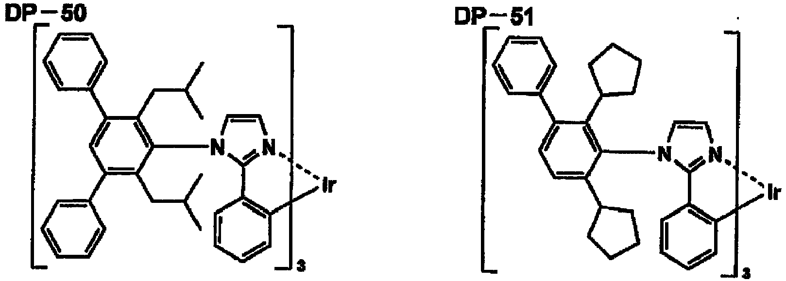


- In Formula (H1), examples of an aromatic hydrocarbon ring or aromatic heterocycle which may have a substituent represented by Q are cited the same aromatic hydrocarbon ring or aromatic heterocycle represented by Ar in Formula (1).
- Examples of a substituent on an aromatic hydrocarbon ring or aromatic heterocycle of Q are cited the same substituents represented by R' and R" in Formula (H2) which will be described later.
- In Formula (H1), examples of a substituted or non-substited condensed heterocycle which is represented by "L" include: an indole ring, a benzimidazole ring, a benzothiazole ring, a benzoxazole ring, a quinoxaline ring, a quinazoline ring, a phthalazine ring, a thienothiophene ring, a condensed aromatic heterocycle containing 3 or more rings (here, as a condensed aromatic heterocycle containing 3 or more rings, it is preferable that it is an aromatic heterocycle containing at least one hetero atom selected from N, O and S as a constituting element to form a condensed ring), specifically, a carbazole ring, and an azacarbazole ring (indicating a ring structure in which one or plural carbon atoms in the ring constituting the aforesaid carbazole ring is replaced with one or plural nitrogen atoms), a dibenzosilole ring, a dibenzofuran ring, a dibenzothiophene ring, a ring in which one or more arbitral carbon atoms which constitutes a benzothiophene ring or a dibenzofuran ring are replaced with nitrogen atoms, a benzodifuran ring, a benzodithiophene ring, an acridine ring, a benzoquinoline ring, a phenazine ring, a phenanthridine ring, a phenanthroline ring, a cycladine ring, a quindoline ring, a thebenidine ring, a quinindoline ring, a triphenodithiazine ring, a triphenodioxazine ring, a phenanthrazine ring, an anthrazine ring, a perimidine ring, a naphthofuran ring, a naphthothiophene ring, a naphthodifuran ring, a naphthodithiophene ring, an anthafuran ring, an anthradifuran ring, an anthrathiophene ring, an anthradithiophene ring, a thianthrene ring, a phenoxathiine ring, a dibenzocarbazole ring, an indrocarbazole ring and a dithienobenzene ring.
- Examples of a substituent on a condensed aromatic heterocycle in L are cited the same substituents represented by R' and R" in Formula (H2) which will be described later.
- L is preferably a condensed aromatic heterocycle formed with 3 or more rings. In particular, L is preferably an aromatic heterocycle represented by Formula (H2').
- In Formula (H2'), A' represents an oxygen atom, a sulfur atom, or NR"'; A'11 to A'18 each respectively represent a nitrogen atom or CR"". Preferably, all of A'11 to A'18 represent CR"".
- In Formula (H2'), R'" and R"" each respectively represent a linking position, a hydrogen atom, or a substituent, provided that when there are a plurality of CR""s, each CR"" may be the same or different, and the plurality of CR""s may be joined to form a ring.
- Examples of a substituent represented by R"'and R"" are cited the same substituents represented by R' and R" in Formula (H2) which will be described later.
- In Formula (H1), n and m each respectively represent an integer of 1 to 3, provided that when n is 2 or more, a plurality of Ls may be the same or different with each other, when m is 2 or more, a plurality of Qs may be the same or different with each other. Preferably, m + n is equal to 3 or more.
- The compound represented by Formula (H1) includes a structure represented by Formula (H2) in the molecule.
- In Formula (H2), A represents an oxygen atom a sulfur atom, NR', or CR" = CR"; and A11 to A23 each respectively represent a nitrogen atom or CR". Preferably, A represents an oxygen atom, a sulfur atom, or NR'. In addition, preferably all of A11 to A23 represent CR".
- In Formula (H3), R' and R" each respectively represent a linking position to other group, a hydrogen atom, or a substituent, provided that when there are a plurality of CR"s, each CR" may be the same or different, and the plurality of CR"s may be joined to form a ring.
- In Formula (H2), examples of a substituted represented by R' and R" include: an alkyl group (for example a methyl group, an ethyl group, a propyl group, an isopropyl group, a tert-butyl group, a pentyl group, a hexyl group, an octyl group, a dodecyl group, a tridecyl group, a tetradecyl group, and a pentadecyl group); an alkenyl group (for example, a vinyl group and an allyl group); an alkynyl group (for example, an ethynyl group and a propargyl group); a non-aromatic hydrocarbon ring with a mono valence derived from the following: a cycloalkyl group (for example, a cyclopentyl group and cyclohexyl group), a cycloalkoxy group (for example a cyclopentyloxy group and a cyclohexyloxy group), a cycloalkylthio group (for example, a cyclopentylthio group and a cyclohexylthio group), a tetrahydronaphthalene ring, a 9,10-dihydroanthracene ring, and a biphenylene ring); a non-aromatic heterocycle with a mono valence derived from the following an epoxy ring an aziridine ring, a thiirane ring, an oxetane ring, an azetidine ring, a thiethane ring, a tetrahydrofuran ring, a dioxolane ring, a pyrrolidine ring, a pyrazolidine ring, an imidazolidine ring, an oxazolidine ring, a tetrahydrothiophene ring, a sulfolane ting, a thiazolidine ring, an ε-caprolactone ring, an ε-caprolactam ring, a piperidine ring, a hexahydropyridazine ring, a hexahydropyrimidine ring, a piperazine ring, a morpholine ring, a tetrahydropyran ring, a 1,3-dioxane ring, a 1,4-dioxane ring, a trioxane ring, a tetrahydrothiopyran ring, a thiomorpholine ring, a thiomorpholine-1,1dioxide ring, a pyranose ring, a diazabicyclo [2,2,2]-octane ring, phenoxazine ring, a phenothiazine ring, an oxanthrene ring, a thioxanthene ring, and a phenoxathiin ring; an aromatic hydrocarbon group with a mono valence derived from the following: a benzene ring, a biphenyl ring, a naphthalene ring, an azulene ring, an anthracene ring, a phenanthrene ring, a pyrene ring, a chrysene ring, a naphthacene ring, a triphenylene ring, o-terphenyl ring, m-terphenyl ring, p-terphenyl ring, an acenaphthene ring, a coronene ring, a fluorene ring, a fluoanthrene ring, a naphthacene ring, a pentacene ring, a perylene ring, a pentaphene ring, a picene ring, a pyrene ring, a pyranthrene ring and an anthraanthrene ring; an aromatic heterocycle with a mono valence derived from the following: a silole ring, a furan ring, a thiophene ring an oxazole ring, a pyrrole ring, a pyridine ring, a pyridazine ring, a pyrimidine ring, a pyrazine ring, a triazine ring, an oxadiazole ring, a triazole ring, an imidazole ring, a pyrazole ring, a thiazole ring, an indole ring, a benzimidazole ring, a benzothiazole ring, a benzoxazole ring, a quinoxaline ring a quinazoline ring, a phthalazine ring, a thienothiophene ring, a carbazole ring, and an azacarbazole ring (indicating a ring structure in which one or plural carbon atoms in the constituting the aforesaid carbazole ring is replaced with one or plural nitrogen atoms), a dibenzosilole ring, a dibenzofuran ring, a dibenzothiophene ring, a ring in which one or more arbitral carbon atoms which constitutes a benzothiophene ring or a dibenzofuran ring are replaced with nitrogen atoms, a benzodifuran ring, a benzodithiophene ring, an acridine ring, a benzoquinoline ring, a phenazine ring, a phenanthridine ring, a phenanthroline ring, a cycladine ring, a quindoline ring, a thebenidine ring, a quinindoline ring, a triphenodithiazine ring, a triphenodioxazine ring, a phenanthrazine ring, an anthrazine ring, a perimidine ring, a naphthofuran ring, a naphthothiophene ring, a naphthodifuran ring, a ring, an anthrafuran ring, an anthradifuran ring, an anthrathiophene ring, an anthradithiophene ring, a thianthrene ring, a phenoxathiine ring, a dibenzocarbazole ring, an indrocarbazole ring and a dithienobenzene ring; an alkoxyl group (for example, a methoxy group, an ethoxy group, a propyloxy group, a pentyloxy group, an hexyloxy group, an octyloxy group, and a dodecyloxy group); an aryloxy group (for example, a phenoxy goup and a naphthyloxy group); an alkylthio group (for example, a methylthio group, an ethylthio group, a propylthio group, a pentylthio group, a hexylthio group, an octylthio group, and a dodecylthio group); an arylthio group (for example, a phenylthio group and a naphthylthio group); an alkoxycarbonyl group (for example, a methyloxycarbonyl group, an ethyloxycarbonyl group, a butyloxycarbonyl group, an octyloxycarbonyl goup, and a dodecyloxycarbonyl group); an aryloxycarbonyl group (for example a phenyloxycarbonyl group and a naphthyloxycarbonyl group); a sulfamoyl group (for example, an aminosulfonyl group, a methylaminosulfonyl group, a dimethylaminosulfonyl group, a butylaminosulfonyl group, a hexylaminosulfonyl group, a cyclohexylaminosulfonyl group, an octylaminosulfonyl group, a dodecylaminosulfonyl group, a phenylaminosulfonyl group, a naphthylaminosulfonyl group, and a 2-pyridylaminosulfonyl group); an acyl group (for example, an acetyl group, an ethylcarbonyl group, a propylcarbonyl group, a pentylcarbonyl group, a cyclohexylcarbonyl group, an octylcarbonyl group, a 2-ethylhexylcarbonyl group, a dodecylcarbonyl group, a phenylcarbonyl group, a naphatylcarbonyl group, and a pyridylcarbonyl group); an acyloxy group (for example, an acetyloxy group, an ethylcarbonyloxy group, a butylcarbonyloxy group, an octylcarbonyloxy group, a dodecylcarbonyloxy group, and a phenylcarbonyloxy group); an amid group (for example, a methylcarbonylamino group, an ethylcarbonylamino group, a dimethylcarbonylamino group, a propylcarbonylamino group, a pentylcarbonylamino group, a cyclohexylcarbonylamino group, a 2-ethylhexylcarbonylamino group, an octylcarbonylamino group, a dodecylcarbonylamino group, a phenylcarbonylamino group, and a naphthylcarbonylamino group); a carbamoyl group (for example, an aminocarbonyl group, a methylaminocarbonyl group, a dimethylaminocarbonyl group, a propylaminocarbonyl group, a pentylaminocarbonyl group, a cyclohexylaminocarbonyl group, an octylaminocarbonyl group, a 2-ethylhexylaminocarbonyl group, a dodecylaminocarbonyl group, a phenylaminocarbonyl group, a naphthylaminocarbonyl group, and a 2-pyridylaminocarbonl group); a ureido group (for example, a methylureido group, an ethylureido group, a pentylureido group, a cyclohexylureido group, an octylureido group, a dodecylureido group, a phenylureido group, a naphthylureido group, and a 2-oyridylaminoureido group); a sulfinyl group (for example, a methylsulfonyl group, an ethylsulfinyl group, a butylsufinyl group, a cyclohexylsulfinyl group, a 2-ethylhexylsulfinyl group, a dodecylsulfinyl group, a phenylsulfinyl group, a naphthylsulfinyl group, and a 2-pyridylsulfinyl group); an alkylsulfonyl group (for example, a methylsulfonyl group, an ethylsulfonyl group, a butylsulfinyl group, a cyclohexylsulfunyl group, a 2-ethylhexylsulfonyl group, and a dodecylsulfonyl group, an arylsulfonyl group or a heteroarylsulfonyl group (for example, a phenylsulfonyl group, a naphthylsolfunyl group, and a 2-pyridylsulfunyl group); an a amino group (for example, an amino group, an ethylamino group, a dimethylamino group, a butylamino group, a cyclopentylamino group, a dodecylamino group, an anilino group, a naphthylamino group, and a 2-pyridylamino group); a halogen atom (for example, a fluorine atom, a chlorine atom, and a bromine atom); a fluoro hydrocarbon group (for example, a fluoromethyl group, trifluoromethyl group, a pentafluoromethyl group, and a pentafluorophenyl group); a cyano group; a nitro group; a hydroxyl group; a mercapto group; a silyl group (for example, a trimethylsilyl group, a triisopropylsilyl group, a triphenylsilyl group, and a phenyldiethylsiyl group); and a phosphono group.
- The structure represented by Formula (H2) is preferably represented by Formula (H2-1) or Formula (H2-2)

- In Formula (H2-1) or Formula (H2-2), A and A11 to A23 each are synonymous with A and A11 to A23 in Formula (H2), respectively.
- The compounds represented by Formula (H1) are preferably further represented by Formulas (H3) to (H102).
- In Formulas (H3) to (H102), L and Q each are synonymous with L and Q in Formula (H1).
- In Formulas (H3) to (H102), at least on of Ls is preferably a carbazole ring. Further, it is preferable that at least one of L-Q in Formulas (H1) and (H3) to (H102) is represented by any one of Formulas (H2), (H2-1) and (H2-2).
- It is preferable that a host compound has a high glass transition temperature (Tg) from the viewpoints of aging stability and aptitude for producing an element. Preferably, Tg of a compound represented by Formula (H1) is 100 °C or more, more preferably, it is 120°C or more, and still more preferably, it is 130 °C or more.
- It is preferable that the compound represented by Formula (H1) has a higher excited triplet energy (T1) than the blue phosphorescence organic metal complex which is used in combination of the compound represented by Formula (H1). Preferably, T1 of the compound represented by Formula (H1) is 2.7 eV or more, more preferably, it is 2.75 eV or more, and still more preferably, it is 2.8 eV or more.
- Here, T1 the compound represented by Formula (H1) is defined as a value calculated employing Gaussian98 (Gauaaian98, Revision A. 11. 4, MJ. Frisch, et al., Gaussian, Inc, Pittsburgh PA, 2002), which is a molecular orbital calculation software, produced by Gaussian Co. in the United State of America, and by employing B3LYP/6-31G* as a key word to obtain an optimize structure, then the value (in terms of corresponding eV unit) is computed. The background, in which the resulting calculated values are effective, is that the calculated values obtained by the above method exhibit high relationship with the experimental values.
- The molecular weigh of the compound represented by Formula (H1) is preferably 500 to 2,000, and it is more preferably 700 to 1,500.
- Specific examples ofa compound represented by Formulas (H3) to (H102) of the present invention are shown below, however, the present invention is not limited to these.


- The layers which constitute the organic EL element of the present invention will now be detailed. Preferred embodiments of the organic EL element of the present invention will be described below, however, the present invention is not limited to these.
- (i) Anode/ light emitting layer/ electron transport layer/ cathode
- (ii) Anode/ hole transport layer/ light emitting layer/ electron transport layer/cathode
- (iii) Anode/ hole transport layer/ light emitting layer/ hole blocking layer/ electron transport layer/cathode
- (iv) Anode/hole transport layer/light emitting layer/hole blocking layer/electron transport layer/cathode buffer layer/cathode
- (v) Anode/ anode buffer layer/hole transport layer/light emitting layer/hole blocking layer/electron transport layer/cathode buffer layer/cathode
- (vi) Anode/ hole transport layer/ anode buffer layer/ light emitting layer/ hole blocking layer/ electron transport layer/ cathode buffer layer/ cathode
- (vii) Anode/ anode buffer layer/ hole transport layer/ light emitting layer/ electron transport layer/cathode buffer layer/ cathode
- Further, it may be provided with a non-light emitting intermediate layer between the light emitting layers when plural light emitting layers are incorporated. In addition, it is possible to make a light emitting unit composed of organic layers including a light emitting layer excluding an anode and a cathode among the above-described constituting layers, and it is possible to laminate a plurality of light emitting units. In the plurality of light emitting units laminated, it may be provided with a non-light emitting intermediate layer between the light emitting units, and the intermediate layer may contain a change generating layer.
- The organic EL element of the present invention have preferably a white light emitting layer, and a lighting device employing this element is preferred.
- Each of the layers which constitute the organic EL elements of the present invention will now be detailed.
- The light emitting layer of the present invention is a layer, which emits light via recombination of electrons and holes injected from an electrode or a layer such as an electron transport layer or a hole transport layer. The light emission portion may be present either within the light emitting layer or at the interface between the light emitting layer and an adjacent layer thereof.
- The total thickness of the light emitting layer is not particularly limited. However, in view of the layer homogeneity, the minimization of application of unnecessary high voltage during light emission, and the stability enhancement of the emitted light color against the drive electric current, the layer thickness is regulated preferably in the range of 2 nm-5 µm, more preferably in the range of 2 nm - 200 nm, but most preferably in the range of 5 nm -100 nm.
- The light emitting layer can be prepared by forming a thin layer made of a light emitting dopant and a host compound, which will be described later, with a vacuum evaporation method or a wet preparation method. A wet preparation method is also called as a wet process, and examples of this include: a spin coating method, a cast method, a die coating method, a blade coating method, a roll coating method, an inkjet method, a printing method, a spray coating method, a curtain coating method, and a LB method (Langmuir Blodgett method).
- It is preferable that the light emitting layer of the organic EL element of the present invention incorporates at least two kinds of compounds: one is a light emitting dopant compound (a phosphorescent emitting dopant (or it is called as a phosphorescence dopant or a phosphorescence emitting dopant group) or a fluorescent dopant) and the other is a light emitting host compound. At least one of the light emitting dopants is a blue phosphorescence organic metal complex represented by the aforementioned Formula (1) or Formula (2), and at least one of the light emitting host compounds is a compound represented by the aforementioned Formula (H1).
- The light emitting dopant compounds (it may be called as the light emitting dopants) of the present invention will now be described.
- As light emitting dopants according to the present invention, it can be employed fluorescent dopants (also referred to as fluorescent compounds) and phosphorescent dopants (also referred to as phosphorescent emitting materials, phosphorescent compounds or phosphorescence emitting compounds).
- A phosphorescence dopant of the present invention will be described.
- The phosphorescent dopant of the present invention is a compound, wherein emission from an excited triplet state thereof is observed, specifically, emitting phosphorescence at room temperature (25 °C) and exhibiting a phosphorescence quantum yield of 0.01 or more at 25 °C. The phosphorescence quantum yield is preferably 0.1 or more.
- The phosphorescence quantum yield can be determined via a method described in page 398 of Bunko II of Dai 4 Han Jikken Kagaku Koza 7 (Spectroscopy II of 4th Edition Lecture of Experimental Chemistry 7) (1992, published by Maruzen Co., Ltd.). The phosphorescence quantum yield in a solution can be determined using appropriate solvents. However, it is only necessary for the phosphorescent dopant of the present invention to exhibit the above phosphorescence quantum yield (0.01 or more) using any of the appropriate solvents.
- Two kinds of principles regarding emission of a phosphorescent dopant are cited. One is an energy transfer-type, wherein carriers recombine on a host compound on which the carriers are transferred to produce an excited state of the host compound, and then via transfer of this energy to a phosphorescent dopant, emission from the phosphorescence-emitting dopant is realized. The other is a carrier trap-type, wherein a phosphorescence-emitting dopant serves as a carrier trap and then carriers recombine on the phosphorescent dopant to generate emission from the phosphorescent dopant. In each case, the excited state energy of the phosphorescent dopant is required to be lower than that of the host compound.
- The light emitting layer of the present invention may further incorporate the compounds described in the following patent documents.
- The patent documents are:
WO 00/70655 JP-A Nos. 2002-280178 2001-181616 2002-280179 2001-181617 2002-280180 2001-247859 2002-299060 2001-313178 2002-302671 2001-345183 2002-324679 WO 02/15645 JP-A Nos. 2002-332291 2002-50484 2002-322292 2002-83684 2002-540572 JP-A Nos. 2002-117978 2002-338588 2002-170684 2002-352960 WO 01/93642 JP-A Nos. 2002-50483 2002-100476 2002-173674 2002-359082 2002-175884 2002-363552 2002-184582 2003-7469 2002-525808 JP-A No. 2003-7471 2002-525833 JP-A Nos. 2003-31366 2002-226495 2002-234894 2002-235076 2002-241751 2001-319779 2001-319780 2002-62824 2002-100474 2002-203679 2002-343572 2002-203678 - As fluorescent dopants, listed are compounds exhibiting a high fluorescent quantum efficiency such as: coumarin based dyes, pyran based dyes, cyanine based dyes, croconium based dyes, squarylium based dyes, oxobenzanthracene based dyes, fluorescein based dyes, Rhodamine based dyes, pyrylium based dyes, perylene based dyes, stilbene based dyes, polythiophene based dyes, rare earth complex based fluorescent materials, or laser dyes.
- Moreover, two or more sorts of compounds may be combined together and used fur the light emitting dopants of the present invention. It is possible to use in combination with phosphorescence dopants each having a different structure or to use in combination of a fluorescence dopant and a phosphorescence dopant.
- Specific examples of a phosphorescent dopant compound which can be preferably used in the present invention will be listed. However, the present invention is not limited to these.


- "Host compounds", as described in the present invention, are defined as compounds, incorporated in a light emitting layer, which result in a weight ratio of 20% or more in the above layer and also result in a phosphorescent quantum yield of the phosphorescence emission of less than 0.1 at room temperature (25°C). Preferably, the phosphorescent quantum yield is less than 0.01. Further, among the compounds incorporated in the light emitting layer, it is preferable that the weight ratio of the host compound in the aforesaid layer is 20% or more.
- The light emitting hosts which can be employed in the present invention are not particularly limited. Although the conventionally known host compounds in organic EL elements can be used particularly preferable host compound used with the blue phosphorescence compound in the light emitting layer of the present invention is a compound represented by the aforementioned Formula (H1) relating to the present invention.
- The conventionally known host compounds may be used with the in organic EL elements can be used with the compound represented by Formula (H1) relating to the present invention. Representative compounds include those having a basic skeleton such as carbazole derivatives, triarylamine derivatives, aromatic compound derivatives, nitrogen-containing heterocyclic compounds, thiophene derivatives, furan derivatives, oligoarylene compounds, carboline derivatives, or diazacarbazole derivatives (here, "a diazacarbazole derivative" indicates a compound having a structure in which at least one of the carbon atoms in a hydrocarbon ring constituting the carboline ring is replaced with a nitrogen atom).
- A known light emitting host (or emission host) which may be used in the present invention is preferably a compound having a hole transporting ability and an electron transporting ability, as well as preventing elongation of an emission wavelength and having a high Tg (a glass transition temperature). Preferably, the host compound has Tg of 100 °C or more.
- It is possible to control the transfer of charges by making use of a plurality of host compounds, which results in high efficiency of an organic EL element.
- In addition, it is possible to mix a different emission lights by making use of a plurality of known phosphorescent dopants as described above. Any required emission color can be obtained thereby.
- Further, an emission host used in the present invention may be either a low molecular weight compound or a polymer compound having a repeating unit, in addition to a low molecular weight compound provided with a polymerizing group such as a vinyl group and an epoxy group (an polymerizable Emission host). These compounds may be used singly or in combination of two or more compounds.
- As specific examples ofaknown emission host compound, the compounds described in the following documents are preferable.
- For example,
JP-A Nos. 2001-257076 2002-308855 2001-313179 2002-319491 2001-357977 2002-334786 2002-8860 2002 334787 2002-15871 2002 334788 2002-43056 2002-334789 2002-75645 2002-338579 2002-105445 2002-343568 2002-141173 2002-352957 2002-203683 2002-363227 2002-231453 2003-3165 2002-234888 2003-27048 2002-255934 2002-260861 2002-280183 2002-299060 2002-302516 2002-305083 2002-305084 2002-308837 - Specific known compounds used as an emission host in the light emitting layer of the organic EL element of the present invention are compounds described in
WO 2011/132493 , paragraphs [0100] to [0110], for example. However, the present invention is not limited to these. - An injection layer is appropriately provided and there are two types: an electron injection layer and a hole injection layer, which may be arranged between an anode and a light emitting layer or a hole transport layer, and between a cathode and a light emitting layer or an electron transport layer, as described above.
- An injection layer is a layer which is arranged between an electrode and an organic layer to decrease an operating voltage and to improve an emission luminance, which is detailed in volume 2, chapter 2 (pp. 123 - 166) of "Organic EL Elements and Industrialization Front thereof (Nov. 30th 1998, published by N. T. S Corp.)", and includes a bole injection layer (an anode buffer layer) and an electron injection layer (a cathode buffer layer).
- An anode buffer layer (a hole injection layer) is also detailed in such as
JP-A Nos. 9-45479 9-260062 8-288069 JP-A Nos. 2003-519432 2006-135145 - A cathode buffer layer (an electron injection layer) is detailed in
JP-A Nos. 6-325871 9-17574 10-74586 - The material used for an anode buffer layer or fro a cathode buffer layer can be used in combination with other material. For example, it is possible to use by mixing in a hole transport layer or in an electron transport layer.
- A bole transport layer contains a material having a function of transporting a hole, and in a broad meaning a hole injection layer and an electron blocking layer are also included in a hole transport layer. A single layer of or plural layers of a hole transport layer may be provided.
- A hole transport material is those having any one of a property to inject or transport a hole or a barrier property to an electron, and may be either an organic substance or an inorganic substance. For example, listed are a triazole derivative, an oxadiazole derivative, an imidazole derivative, a polyarylalkane derivative, a pyrazolone derivative, a phenylenediamine derivative, an arylamine derivative, an amino substituted chalcone derivative, an oxazole derivatives, a styrylanthracene derivative, a fluorenone derivative, a hydrazone derivative, a stilbene derivative, a silazane derivative, an aniline type copolymer, or conductive polymer oligomer and specifically preferably such as thiophene oligomer. Further, an azatriphenylene derivative described in
JP-A Nos. 2003-519432 2006-135145 - As a hole transport material, those described above can be utilized, however, it is preferable to utilized a porphyrin compound, an aromatic tertiary amine compound and a styrylamine compound, and specifically preferably an aromatic tertiary amine compound.
- Typical examples of an aromatic tertiary amine compound and a styrylamine compound include: N,N,N',N'-tetraphenyl-4,4'-diaminophenyl; N,N'-diphenyl-N,N'-bis(3-methylphenyl)-(1,1'-biphenyl)-4,4'-diamine(TDP); 2,2-bis(4-di-p-tolylaminophenyl)propane; 1,1-bis(4-di-p-tolylaminophenyl)cyclohexane; N,N,N',N'-tetra-p-tolyl 4,4'-diaminobiphenyl; 1,1-bis(4-di-p-tolylaminophenyl)-4-phenylcyclohexane; bis(4-dimethylamino-2-metyl)phenylmethane; bis(4-di-p-tolylaminophenyl)phenylmethane; N,N'-diphenyl-N,N'-di(4-methoxyphenyl)-4,4'-diaminobiphenyl; N,N, N',N'-tetraphenyl-4,4'-diaminophenylether; 4,4'-bis(diphenylamino)quadriphenyl; N,N,N-tri(p-tolyl)amine; 4-(di-p-tolylamino)-4'-[4-(di-p-triamino)styryl]stilbene; 4-N,N-diphenylamino-(2-diphenylvinyl)benzene; 3-methoxy-4'-N,N-diphenylaminostilbene; and N-phenylcarbazole, in addition to those having two condensed aromatic rings in the molecule described in USP No.
5,061,569 , such as 4,4'-bis[N-(1-naphthyl)-N-phenylamino]biphenyl (NDP), and 4,4',4"-tris[N-(3-methylphenyl)-N-phenylamino]triphenylamine (MDTDATA), in which three of triphenylamine units are bonded in a star burst form, described inJP-A No. 4-308688 - Polymer materials, in which these materials are introduced in a polymer chain or constitute the main chain of polymer, can be also utilized.
- Further, an inorganic compound such as a p type-Si and a p type-SiC can be utilized as a hole injection material and a hole transport material.
- Moreover, it cam be used a cyclometalated complex and an orthometalated complex such as Copper phthalocyanine and tris(2-phenylpyridine) indium as a hole transport material.
- Further, it is possible to employ so-called p type hole transport materials, as described in Japanese Patent Publication Open to Public Inspection (referred to as
JP-A) No.11-251067 - This hole transport layer can be prepared by forming a thin layer made of the above-described hole transport material according to a method well known in the art such as a vacuum evaporation method, a spin coating method, a cast method, an inkjet method and a LB method.
- The layer thickness of a hole transport layer is not specifically limited, however, it is generally 5nm - 5µm, and preferably 5 nm - 200nm. This hole transport layer may have a single layer structure comprised of one or plural types of the above described materials.
- Further, it is possible to employ a hole transport layer of a higher p property which is doped with impurities. As its example, listed are those described in each of
JP-A Nos. 4-297074 2000-196140 2001-102175 - In the present invention, it is preferable to employ a hole transport layer of such a high p property, since it is possible to produce an element of lower electric power consumption.
- There are given examples of the compound preferably used for formation of the hole transport layer of the organic EL element of the present invention. However, the present invention is not limited to these.


- An electron transport layer is composed of a material having a function to transfer an electron, and an electron injection layer and a hole blocking layer are included in an electron transport layer in a broad meaning. A single layer or plural layers of an electron transport layer may be provided.
- As an electron transport material (including a hole blocking material and an electron injection material) used for an electron transport layer is only required to have a function of transporting electrons ejected from the cathode to the light emitting layer. As materials to form an electron transport layer, any of the conventional compounds may be selected and they can be singly or jointly.
- Examples of them (hereinafter, they are called as an electron transport material) include: a nitro-substituted fluorene derivative, a diphenylquinone derivative, a thiopyradineoxide derivative, heterocyclic tetracarboxylic acid anhydride such as naphtalene perylene, carbodiimide, a fluorenylidenemethane derivative, anthraquinonedimethane, an anthrone derivative, an oxadiazole derivative, a carboline derivative and an azacarbazole derivative.
- Here, "an azacarbazole derivative" indicates a compound having a structure in which at least one of the carbon atoms constituting the carboline ring is replaced with one or more nitrogen atoms.
- Further, as examples of an oxadiazole derivative described above, the following compounds can be used as an electron transport material: a thiadiazole derivative in which an oxygen atom in the oxadiazole ring is replaced with a sulfur atom; and a quinoxaline derivative which contains a quinoxaline ring known as an electron withdrawing group.
- Polymer materials, in which these materials are introduced in a polymer chain or these materials form the main chain of polymer, can be also utilized.
- Further, a metal complex of a 8-quinolinol derivative such as tris(8-quinolinol)aluminum (Alq3), tris(5,7-dichloro-8-quinolinol)aluminum, tris(5,7-dibromo-8-quinolinol)aluminum, tris(2-methyl-8-quinolinol)aluminum, tris(5-methyl-8-quinolinol)aluminum and bis(8-quinolinol)zinc (Znq); and metal complexes in which a central metal of the aforesaid metal complexes is substituted by In, Mg, Cu, Ca, Sn, Ga or Ph, can be also utilized as an electron transport material.
- Further, metal-free or metal phthalocyanine, or a compound whose terminal is substituted by an alkyl group or a sulfonic acid group, can be preferably utilized as an electron transport material.
- In the same manner as for a hole injection layer and hole transport layer, an inorganic semiconductor such as an n-type-Si and an n-type-SiC can be also utilized as an electron transport material.
- The preparation method of the constituting layers of the organic EL element will be described in detain in the portion of preparation of an organic EL element.
- The layer thickness of the electron transport layer of the present invention is not specifically limited; however, it is generally 5 nm-5,000 nm, and preferably it is 5 nm-200nm. This electron transport layer may be a single layer structure containing of one or more types of the above described materials.
- Further, it is possible to employ an electron transport layer of a higher n property which is doped with impurities. As its example, listed are those described in each of
JP-A Nos. 4-297076 10-270172 200-196140 2001-102175 - Next, there will be listed specific example compounds (electron transport materials) known in the art and preferably used in the electron transport layer of the white light emitting organic EL element. However, the present invention is not limited to them.


- A blocking layer is appropriately provided in addition to the basic constitution layers composed of organic thin layers as described above. Examples are described in such as
JP-A Nos.11-204258 11-204359 - A hole blocking layer, in broad meaning, is provided with a function of electron transport layer, being comprised of a material having a function of transporting an electron but a very small ability of transporting a hole, and can improve the recombination probability of an electron and a hole by blocking a hole while transporting an electron.
- Further, a constitution of an electron transport layer described above can be appropriately utilized as a hole blocking layer according to the present invention.
- The hole blocking layer of the organic EL element of the present invention is preferably arranged adjacent to the light emitting layer.
- It is preferable that the hole blocking layer incorporates a nitrogen containing compound such as a carbazole derivative, an azacarbazole derivative (here, "an azacarbazole derivative" indicates a compound having a structure in which at least one of the carbon atoms constituting the carboline ring is replaced with one or more nitrogen atoms), or a pyridine derivative.
- Further, in the present intention, in the case in which a plurality of light emitting layers which differ in a plurality of different emitted light colors, it is preferable that the light emitting layer which results in the shortest wavelength of the emitted light maximum wavelength is nearest to the anode in all light emitting layers. However, in such a case, it is preferable to additionally arrange the hole blocking layer between the aforesaid shortest wavelength layer and the light emitting layer secondly near the anode.
- Further, at least 50% by weight of the compounds incorporated in the hole blocking layer arranged in the aforesaid position preferably exhibits the ionization potential which is greater by at least 0.3 eV than that of the host compounds of the aforesaid shortest wavelength light emitting layer.
- The ionization potential is defined as energy which is necessary 10 release electrons in the HOMO (being the highest occupied molecular orbital) to the vacuum level, and be determined via for example, the method described below.
- (1) By employing Gaussian98 (Gauaaian98, Revision A. 11. 4, M.J. Frisch, et al. Gaussian 98(Gaussian98, Revision A. 11.4, M.J. Frisch, et al, Gaussian, Inc., Pittsburg hPA, 2002), which is a molecular orbital calculation software, produced by Gaussian Co. in the United State of America, and by employing B3LYP/6-31G* as a key word, the value (in terms of corresponding eV unit) was computed, and it is possible to obtain the ionization potential by rouging off the second decimal point The background, in which the resulting calculated values are effective, is that the calculated values obtained by the above method exhibit high relationship with the experimental values. (2) It is possible to determine the ionization potential via a method in which ion potential is directly determined employing a photoelectron spectrometry. For example, by employing a low energy electron spectrophotometer "Model AC-1" produced by Riken Keiki Co., or appropriately employ a method known as an ultraviolet light electron spectrometry.
- On the other hand, the electron blocking layer, as described herein, has a function of the hole transport layer in a broad sense, and is composed of materials having markedly small capability of electron transport, while having capability of transporting holes and enhance the recombination probability of electrons and holes by inhibiting electrons, while transporting electrons.
- Further, it is possible to employ the constitution of the hole transport layer, described below, as an electron blocking layer when needed. The thickness of the hole blocking layer and the electron transport layer according to the present invention is preferably 3 -100 mn, but is more preferably 3 - 30 nm.
- As an anode according to an organic EL element of the present invention, those comprising metal, alloy, a conductive compound, which is provided with a large work function (not less than 4eV), and a mixture thereof as an electrode substance are preferably utilized. Specific examples of such an electrode substance include a conductive transparent material such as metal like Au, CuI, indium tin oxide (ITO), SnO2 and ZnO.
- Further, a material such as IDIXO (In2O3-ZnO), which can prepare an amorphous and transparent electrode, may be also utilized As for an anode, these electrode substances may be made into a thin layer by a method such as evaporation or spattering and a pattern of a desired form may be formed by means of photolithography, or in the case of requirement of pattern precision is not so severe (about 100 µm or more), a pattern may be formed through a mask of a desired form at the time of evaporation or spattering of the above-described substance.
- Alternatively, when coatable materials such as organic electrically conductive compounds are employed, it is possible to employ a wet system filming method such as a printing system or a coating system. When emission is taken out of this anode, the transmittance is preferably set to not less than 10% and the sheet resistance as an anode is preferably a few hundreds Ω/□D or less. Further, although the layer thickness depends on a material, it is generally selected in the range of 10 mn-1,000 nm and preferably of 10 nm- 200 nm.
- On the other hand, as a cathode according to the present invention, metal, alloy, a conductive compound and a mixture thereof, which have a small work function (not more than 4 eV), are utilized as an electrode substance.
- Specific examples of such an electrode substance includes such as sodium, sodium-potassium alloy, magnesium, lithium, a magnesium/copper mixture, a magnesium/silver mixture, a magnesium/aluminum mixture, a magnesium/indium mixture, an aluminum/aluminum oxide (Al2O3) mixture, indium, a lithium/aluminium mixture and rare earth metal.
- Among them, with respect to an electron injection property and durability against such as oxidation, preferable are: a mixture of electron injecting metal with a second metal which is stable metal having a work function larger than electron injecting metal. Examples thereof are: a magnesium/silver mixture, a magnesium/aluminum mixture, a magnesium/indium mixture, an potassium/aluminum mixture and aluminum.
- As for a cathode, these electrode substances may be made into a thin layer by a method such as evaporation or spattering. Further, sheet resistance as a cathode is preferably not more than a few hundreds Ω/□ and the layer thickness is generally selected in a range of 10 nm- 5 µm and preferably of 50 mn - 200 mn.
- Herein, to transmit produced emission, either one of an anode or a cathode of an organic EL element is preferably transparent or translucent to improve the emission luminance.
- Further, after forming, on the cathode, the above metals at a film thickness of 1 nm - 20 mn, it is possible to prepare a transparent or translucent cathode in such a manner that electrically conductive transparent materials are prepared thereon. By applying the above, it is possible to produce an element in which both anode and cathode are transparent.
- A support substrate according to an organic EL element of the present invention is not specifically limited with respect to types of such as glass and plastics. The support substrate may be also called as substrate body, substrate, substrate substance, or support. They me be transparent or opaque. However, a transparent support substrate is preferable when the emitting light is taken from the side of the support substrate.
- Support substrates preferably utilized includes such as glass, quartz and transparent resin film. A specifically preferable support substrate is a resin film capable of providing an organic EL element with a flexible property.
- Resin films includes such as: polyesters such as polyethylene terephtalate (PET) and polyethylene naphthalate (PEN); polyethylene, polypropylene; cellulose esters or their derivatives such as cellophane, cellulose diacetate, cellulose triacetate, cellulose acetate butylate, cellulose acetate propionate (CAP), cellulose acetate phthalate (TAC) and cellulose nitrate; polyvinylidene chloride, polyvinyl alcohol, polyethylene vinyl alcohol, syndiotactic polystyrene, polycarbonate, norbomene resin, polymethylpentene, polyether ketone, polyimide, polyether sulfone (PES), polyphenylene sulfide, polysulfones, polyetherimide, polyether ketone imide, polyamide, fluororesin, Nylon, polymethylmethacrylate, acrylic resin, polyacrylate; and cycloolefin resins such as ARTON (produced by JSR Co. Ltd.) and APEL (produce by Mitsui Chemicals, Inc.).
- On the surface of a resin film, it may be formed a film incorporating an inorganic or an organic compound or a hybrid film incorporating both compounds. Barrier films are preferred at a water vapor permeability (25±0.5°C, and relative humidity (90±2)%RH) of 0.01 g/(m2·24h) or less, determined based on JIS K 7129-1992. Futher, high barrier films are preferred at an oxygen permeability of 1x10⁻³ ml/(m2·24h·MPa) or less, an at a water vapor permeability of 10-5 g/(m2(m2·24h) or less, determined based on JIS K 7126-1987.
- As materials forming a barrier film, employed may be those which retard penetration of moisture and oxygen, which deteriorate the element. For example, it is possible to employ silicon oxide, silicon dioxide, and silicon nitride.
- Further, in order to improve the brittleness of the aforesaid film, it is more preferable to achieve a laminated layer structure of inorganic layers and organic layers. The laminating of the inorganic layer and the organic layer is not particularly limited, but it is preferable that both are alternatively laminated a plurality of times.
- Barrier film forming methods are not particularly limited, and examples of employable methods include a vacuum deposition method, a sputtering method, a reactive sputtering method, a molecular beam epitaxy method, a cluster ion beam method, an ion plating method, a plasma polymerization method, a plasma CVD method, a laser CVD method, a thermal CVD method, and a coating method. Of there, specifically preferred is a method employing an atmospheric pressure plasma polymerization method, described in
JP-A No. 2004-68143 - Examples of opaque support substrates include metal plates such aluminium or stainless steel, films, opaque resin substrates, and ceramic substrates.
- The external extraction efficiency of light emitted by the organic EL element of the present invention is preferably 1% or more at room temperature, but is more preferably 5% or more.
- External quantum yield (%) = (Number of photons emitted by the organic EL element to the exterior/Number of electrons fed to organic EL element) ×100.
- Further, even by simultaneously employing color hue improving filters such as a color filter, simultaneously employed maybe color conversion filters which convert emitted light color from the organic EL element to multicolor by employing fluorescent materials. When the color conversion filters are employed, it is preferable that λmax of light emitted by the organic EL element is 480 nm or less.
- As one example of the preparation method of the organic EL element of the present invention, there will be described the preparation method of the organic EL element composed of anode/ hole injection layer/hole transport layer/ light emitting layer/ hole blocking layer/ electron transport layer/cathode buffer layer (electron injection layer)/ cathode.
- Initially, a thin film composed of desired electrode substances, for example, anode substances is formed on an appropriate base material to reach a thickness of 1 µm or less, but preferably 10 nm-200 nm, whereby an anode is prepared.
- Subsequently, on the above, formed are organic compound thin layers including a hole injection layer, a hole transport layer, a light emitting layer, a hole blocking layer, an electron transport layer, and a cathode buffer layer, which contain organic materials.
- In the organic EL element of phosphorescence luminescence of the present invention, at least a cathode and an electron transport layer located adjacent to the cathode are preferably coated and formed with a wet process.
- Examples of a wet process include: a spin coating method, a cast method, a die coating method, a blade coating method, a roll coating method, an inkjet method, a printing method, a spray coating method, a curtain coating method, and a LB method. From the viewpoint of enabling to form a precise thin layer with a high productivity, a die coating method, a roll coating method, an inkjet method and a spray coating method are preferably used. These methods are suitable for applying to a roll to roll production method. It may be possible to use a different film production method for every layer.
- As liquid media which are employed to dissolve or disperse organic metal complexes according to the present invention, employed may be, for example, ketones such as methyl ethyl ketone or cyclohexanone, fatty acid esters such as ethyl acetate, halogenated hydrocarbons such as dichlorobenzenes, aromatic hydrocarbons such as toluene, xylene, mesitylene, and cyclohexylbenzene, aliphatic hydrocarbons such as cyclohexane, decaline, and dodecane, and organic solvents such as DMF or DMSO.
- Further, with regard to dispersion methods, it is possible to achieve dispersion employing dispersion methods such as ultrasonic waves, high shearing force dispersion or media dispersion.
- After forming these layers, a thin composed of cathode materials is formed on the above layers so that the film thickness reaches 1 µm or less, but is preferably in the range of 50 - 200 nm, whereby a cathode is arranged, and the desired organic EL element is prepared.
- Further, by revering the preparation, it is possible to achieve preparation in order of a cathode, a cathode buffer layer, an electron injection layer, an electron transport layer, a light emitting layer, a hole transport layer, a hole injection layer, and an anode.
- When direct current voltage is applied to the multicolor display device prepared as above, the anode is employed as (+) polarity, while the cathode is employed as (-) polarity. When 2-40 V is applied, it is possible to observe light emission. Further, alternating current voltage may be applied. The wave form of applied alternating current voltage is not specified.
- It is preferable to produce an organic EL element of the present invention with one vacuum operation, from formation of a hole injection layer to formation of a cathode without interruption. However, it may be possible to interrupt the operation and take out the intermediate product in order to apply a different film forming method. In that case, working under a dry inert gas atmosphere is preferable.
- As sealing means employed in the present invention, listed may be, for example, a method in which sealing members, electrodes, and a supporting substrate are subjected to adhesion via adhesives.
- The sealing members may be arranged to cover the display region of an organic EL element, and may be an engraved plate or a flat plate. Neither transparency nor electrical insulation is limited.
- Specifically listed are glass plates, polymer plate-films, metal plates, and films. Specifically, it is possible to list, as glass plates, soda-lime glass, barium-strontium containing glass, lead glass, aluminosilicate glass, borosilicate glass, barium borosilicate glass, and quartz.
- Further, listed as polymer plates may be polycarbonates, acryl, polyethylene terephthalate, polyether sulfide, and polysulfone. As a metal plate, listed are those composed of at least one metal selected from the group consisting of stainless steel, iron, copper, aluminum magnesium, nickel, zinc, chromium, titanium, molybdenum, silicon, germanium, and tantalum, or alloys thereof.
- In the present invention, since it is possible to convert the element to a thin film, it is possible to preferable employ a metal film.
- Further, the oxygen permeability of the polymer film is preferably 1x10⁻³ ml/(m2·24h·MPa) of less, determined by the method based on JIS K 7126-1987, while its water vapor permeability (at 25 ±0.5°C and relative humidity (90±2)%RH) is 10-5 g/(m2·24h) or less, determined by the method based on JIS K 7129-1992.
- Conversion of the sealing member into concave is carried out employing a sand blast process or a chemical etching process.
- In practice as adhesives, listed may be photo-curing and heat-curing types having a reactive vinyl group of acrylic acid based oligomers and methacrylic acid, as well as moisture curing types such as 2-cyanoacrylates. Further listed may be thermal and chemical curing types (mixtures of two liquids) such as epoxy based ones.
- Still further listed may be hot-melt type polyamides, polyester, and polyolefins. Yet further listed may be cationically curable type ultraviolet radiation curable type epoxy resin adhesives.
- In addition, since an organic EL element is occasionally deteriorated via thermal process, those are preferred which enable adhesion and curing between room temperature and 80°C. Further, desiccating agents may be dispersed into the aforesaid adhesives. Adhesives may be applied onto sealing portions via commercial dispenser or printed on the same in the same manner as screen printing.
- Further, it is appropriate that on the outside of the aforesaid electrode which interposes the organic layer and faces the support substrate, the aforesaid electrode and organic layer are covered, and in the form of contact with the support substrate, inorganic and organic material layers are formed as a sealing film.
- In this case, as materials forming the aforesaid film may be those which exhibit functions to retard penetration of those such as moisture or oxygen which results in deterioration. For example, it is possible to employ silicon oxide, silicon dioxide, and silicon nitride.
- Still further, in order to improve brittleness of the aforesaid film, it is preferable that a laminated layer structure is formed, which is composed of these inorganic layers and layers composed of organic materials.
- Methods to from these films are not particularly limited. It is possible to employ, for example, a vacuum deposition method, a sputtering method, a reactive sputtering method, a molecular beam epitaxy method, a cluster ion beam method, an ion plating method, a plasma polymerization method, an atmospheric pressure plasma polymerization method, a plasma CVD method, a thermal CVD method, and a coating method.
- In a gas phase and a liquid phase, it is preferable to inject inert gases such as nitrogen or argon, and inactive liquids such as fluorinated hydrocarbon or silicone oil into the space between the sealing member and the surface region of the organic EL element. Further, it is possible form vacuum. Still further, it is possible to enclose hygroscopic compounds in the interior. Still further, it is possible to enclose hygroscopic compounds in the interior.
- Examples of hygroscopic compounds include metal oxides (for example, sodium oxide, potassium oxide, calcium oxide, barium oxide, magnesium oxide, and aluminum oxide); sulfates (for example, sodium sulfate, calcium sulfate, magnesium sulfate, and cobalt sulfate); metal halides (for example, calcium chloride, magnesium chloride, cesium fluoride, tantalum fluoride, cerium bromide, magnesium bromide, barium iodide, and magnesium iodide); perchlarates (for example, barium perochlorate and magnesium perchlorate). In sulfates, metal halides, and perchlorates, suitably employed are anhydrides.
- The aforesaid sealing film on the side which nips the organic layer and faces the support substrate or on the outside of the aforesaid sealing film, a protective or a protective plate may be arranged to enhance the mechanical strenght of the element. Specifically, when sealing is achieved via the aforesaid sealing film, the resulting mechanical strength is not always high enough, whereby it is preferable to arrange the protective film or the protective plate described above.
- Usable materials for these include glass plates, polymer plate-films, and metal plate-films which are similar to those employed employed for the aforesaid sealing. However, in terms of light weight and a decrease in thickness, it is preferable to employ polymer films.
- It is generally known that an organic EL element emits light in the interior of the layer exhibiting the refractive index (being about about 1.7 - about 2.1) which is greater than that of air, whereby only about 15 - about 20% of light generated in the light emitting layer is extracted.
- This is due to the fact that light incident to an interface (being an interface of a transparent substrate to air) at an angle of θ which is at least critical angle is not extracted to the exterior of the element due to the resulting total reflection, or light is totally reflected between the transparent electrode or the light emitting layer and the transparent substrate, and light is guided via the transparent electrode or the light emitting layer, whereby light escapes in the direction of the element side surface.
- Means to enhance the efficiency of the aforesaid light extraction include, for example, a method in which roughness is formed on the surface of a transparent substrate, whereby total reflection is minimized at the interface of the transparent substrate to air (
U.S. Patent No. 4,774,435 ), a method in which efficiency is enhanced in such a manner that a substrate results in light collection (JP-A No. 63-314795 JP-A No. 1-220394 JP-A No. 62-172691 JP-A No. 2001-202827 JP-A No. 11-283751 - In the present invention, it is possible to employ these methods while combined with the organic EL element of the present invention. Of these, it is possible to appropriately employ the method in which a flat layer of a refractive index which is equal to or less than the substrate is introduced between the substrate and the light emitting body and the method in which a diffraction grating is formed between the substrate and any of the layers such as the transparent electrode layer or the light emitting layer (including between the substrate and the outside).
- By combining these means, the present invention enables the production of elements which exhibit higher luminance or excel in durability.
- When a low refractive index medium of a thickness, which is greater than the wavelength of light, is formed between the transparent electrode and the transparent substrate, the extraction efficiency of light emitted from the transparent electrode to the exterior increases as the refractive index of the medium decreases.
- As materials of the low refractive index layer, listed are, for example, aerogel, porous silica, magnesium fluoride, and fluorine based polymers. Since the refractive index of the transparent substrate is commonly about 1.5 - 1.7, the refractive index of the low refractive index layer is preferably approximately 1.5 or less, but is more preferably 1.35 or less.
- Further, thickness of the low refractive index medium is preferably at least two times the wavelength in the medium. The reason is that when the thickness of the low refractive index medium reaches nearly the wavelength of light so that electromagnetic waves oozed via evernescent enter into the substrate, effects of the low refractive index layer are lowered.
- The method in which the interface which results in total reflection or a diffraction grating is introduced in any of the media is characterized in that light extraction efficiency is significantly enhanced.
- The above method works as follows. By utilizing properties of the diffraction grating capable of changing the light direction to the specific direction different from diffraction via so-called Bragg diffraction such as primary diffraction or secondary diffraction of the diffraction grating of light emitted from the light emitting layer, light, which is not emitted to the exterior due to total reflection between layers, is diffracted via introduction of diffraction grating between any layers or in a medium (in the transparent substrate and the transparent electrode) so that light is extracted to the exterior.
- It is preferable that the introduced diffraction grating exhibits a two-dimensional periodic refractive index. The reason is as follows. Since light emitted in the light emitting layer is randomly generated to all directions, in a common one-dimensional diffraction grating exhibiting a periodic refractive index distribution only in a certain direction, light which travels to the specific direction is only diffracted, whereby light extraction efficiency is not sufficiently enhanced.
- However, by changing the refractive index distribution to a two-dimensional one, light, which travels to all directions, is diffracted, whereby the light extraction efficiency is enhanced.
- As noted above, a position to introduce a diffraction grating may be between any layers or in a medium (in a transparent substrate or a transparent electrode). However, a position near the organic light emitting layer, where light is generated, is desirous.
- In this case, the cycle of the diffraction grating is preferably about 1/2 - 3 times the wavelength of light in the medium.
- The preferable arrangement of the diffraction grating is such that the arrangement is two-dimensionally repeated in the form of a square lattice, a triangular lattice, or a honeycomb lattice.
- Via a process to arrange a structure such as a micro-lens array shape on the light extraction side of the organic EL element of the present invention or via combination with a so-called light collection sheet, light is collected in the specific direction such as the front direction with respect to the light emitting element surface, whereby it is possible to enhance luminance in the specific direction.
- In an example of the micro-lens array, square pyramids to realize a side length of 30 µm and an apex angle of 90 degrees are two-dimensionally arranged on the light extraction side of the substrate. The side length is preferably 10 µm - 100 µm. When it is less than the lower limit, it will result in coloration due to generation of diffraction effects, while when it exceeds the upper limit, the thickness increases undesirably.
- It is possible to employ, as a light collection sheet, for example, one which is put into practical use in the LED backlight of liquid a crystal display devices. It is possible to employ, as such a sheet, for example, the luminance enhancing film (BEF), produced by Sumitomo 3M limited.
- As shapes of a prism sheet employed may be, for example, Δ shaped stripes of an apex angle of 90 degrees and a pitch of 50 µm formed on a base material, a shape in which the apex angle is rounded, a shape in which the pitch is randomly changed, and other shapes.
- Further, in order to control the light radiation angle from the light emitting element, simultaneously employed may be a light diffusion plate-film. For example, it is possible to employ the diffusion film (LIGHT-UP), produced by Kimoto Co., Ltd.
- It is possible to employ the organic EL element of the present invention as display devices, displays, and various types of light emitting sources. Examples of light emitting sources include, but are not limited to lighting apparatuses (home lighting and car lighting), clocks, backlights for liquid crystals, sign advertisements, signals, light sources of light memory media, light sources of electrophotographic copiers, light sources of light communication processors, and light sources of light sensors.
- It is effectively employed especially as backlights of liquid crystal display devices and lighting sources.
- If needed, the organic EL element of the present invention may undergo patterning via a metal mask or an ink-jet printing method during film formation. When the patterning is carried out, only an electrode may undergo patterning, an electrode and a light emitting layer may undergo patterning, or all element layers may undergo pattering. During preparation of the element, it is possible to employ conventional methods.
- Color of light emitted by the organic EL element of the present invention and compounds according to the present invention is specified as follows. In
FIG. 4 .16 onpage 108 of"Shinpen Shikisai Kagaku Handbook (New Edition Color Science Handbook)" (edited by The Color Science Association of Japan, Tokyo Daigaku Shuppan Kai, 1985 - Further, when the organic EL element of the present invention is a white element, "white", as described herein, means that when 2-degree viewing angle front luminance is determined via the aforesaid method, chromaticity in the CIE 1931 Color Specification System is within the region of X = 033 ± 0.07 and Y = 0.33 ± 0.07.
- A display device of the present invention will now be explained. The display device of the present invention includes the above-described organic EL element.
- A display device of the present invention may be either monochromatic or multi-colored. Here explained will be a multicolor display device.
- In the case of a multicolor display device, a shadow mask is provided only at the time of emission layer formation, and layers can be formed all over the surface by such as an evaporation method, a cast method, a spin coat method, an inkjet method and a printing method.
- When patterning is performed only for producing a light emitting layers, the method is not specifically limited; however, preferable are an evaporation media an inkjet method, a spin coating method and a printing method.
- The constitution of the organic EL element used for a display device can be selected from the embodiments of the organic EL element as described above, in accordance with the requirement.
- The production method of the organic EL element was described above for one of the embodiments of the organic EL element of the present invention.
- When a direct current voltage is applied on the multicolor display device thus prepared, emission can be observed by application of a voltage of approximately 2 - 40 V setting an anode to (+) polarity and a cathode to (-) polarity. Further, no current flows and no emission generate at all even when a voltage is applied with a reversed polarity. Further, in the case of alternate current voltage being applied, emission generates only in a state of an anode being + and a cathode being -. Herein, the wave shape of alternate current may be arbitrary.
- A multicolor display device can be utilized as a display device, a display and various types of emission light sources. In a display device and a display, full-colored display is possible by employing three types of organic EL elements providing blue, red and green emissions.
- A display device and a display include a TV, a personal computer, a mobile instrument, an AV instrument, a character broadcast display and an information display in a car. Particularly, the display device and the display may be also utilized as a display to playback still images and moving images, and may adopt ether a simple matrix (a passive matrix) mode or an active matrix mode when being utilized as a display device for moving image playback.
- An illumination light source includes a home use illumination, a car room illumination, a backlight of a watch or a liquid crystal, a panel advertisement, a signal, a light source of an optical memory medium, a light source for an electrophotographic copier, a light source for an optical telecommunication processor and a light source for a photo-sensor, however, the present invention is not limited thereto.
- In the following, one example of a display device provided with an organic EL element of the present invention will be explained with reference to figures.
-
FIG.1 is a schematic drawing to show an example of a display device constituted of an organic EL element. It is a schematic drawing of a display, which displays image information by emission of an organic EL element, such as a mobile phone. - Display 1 is constituted of display section A having plural number of pixels and control section B which performs image scanning of display section A based on image information.
- Control section B, which is electrically connected to display section A, sends a scanning signal and an image data signal to plural number of pixels based on image information from the outside and pixels of each scanning line successively emit depending on the image data signal by a scanning signal to perform image scanning, whereby image information is displayed on display section A.
-
FIG. 2 is a schematic drawing of display section A. - Display section A is provided with such as a wiring part, which contains
plural scanning lines 5 anddata lines 6, andplural pixels 3 on a substrate. Primary part materials of display section A will be explained in the following. - In the drawing, shown is the case that light emitted by
pixel 3 is taken out along the white allow (downward). -
Scanning lines 5 andplural data lines 6 in a wiring part each are comprised of a conductive material, andscanning lines 5 anddata lines 6 are perpendicular in a grid form and are connected topixels 3 at the right-angled crossing points (details are not shown in the drawing). -
Pixel 3 receives an image data fromdata line 6 when a scanning signal is applied from scanningline 5 and emits according to the received image data. - Full-color display device is possible by appropriately arranging pixels having an emission color in a red region, pixels in a green region and pixels in a blue region, side by side on the same substrate.
- Next, an emission process of a pixel will be explained.
-
FIG. 3 is a schematic drawing of a pixel. - A pixel is equipped with such as
organic EL element 10, switchingtransistor 11, operatingtransistor organic EL element 10 for plural pixels, and full-color display device is possible by arranging these side by side on the same substrate. - In
FIG. 3 , an image data signal is applied on the drain of switchingtransistor 11 viadata line 6 from control section B. Then, when a scanning signal is applied on the gate of switchingtransistor 11 viascanning line 5 from control section B, operation of switching transistor is on to transmit the image data signal applied on the drain to the gates ofcapacitor 13 andoperating transistor 12. -
Operating transistor 12 is on, simultaneously withcapacitor 13 being charged depending on the potential of an image data signal, by transmission of an image data signal. In operatingtransistor 12, the drain is connected toelectric source line 7 and the source is connected to the electrode oforganic EL element 10, and an electric current is supplied fromelectric source line 7 toorganic EL element 10 depending on the potential of an image data applied on the gate. - When a scanning signal is transferred to
next scanning line 5 by successive scanning of control section B, operation of switchingtransistor 11 is off. - However, since
condenser 13 keeps the charged potential of an image data signal even when operation of switchingtransistor 11 is off, operation of operatingtransistor 12 is kept on to continue emission oforganic EL element 10 until the next scanning signal is applied. - When the next scanning signal is applied by successive scanning, operating
transistor 12 operates depending on the potential of an image data signal synchronized to the scanning signal andorganic EL element 10 emits. - That is, emission of each
organic EL element 10 ofplural pixels 3 is performed by providing switchingtransistor 11 andoperating transistor 12 against eachorganic EL element 10 ofplural pixels 3. Such an emission method is called as an active matrix mode. - Herein, emission of
organic EL element 10 may be either emission of plural gradations based on a multiple-valued image data signal having plural number of gradation potentials or on and off of a predetermined emission quantity based on a binary image data signal. Further, potential hold ofcapacitor 13 may be either continuously maintained until the next scanning signal application or discharged immediately before the next scanning signal application. - In the present invention, emission operation is not necessarily limited to the above-described active matrix mode but may be a passive matrix mode in which organic EL element is emitted based on a data signal only when a scanning signal is scanned.
-
FIG. 4 is a schematic drawing of a display device based on a passive matrix mode. InFIG. 4 , plural number ofscanning lines 5 and plural number ofimage data lines 6 are arranged grid-wise opposing to each other and sandwichingpixels 3. - When a scanning signal of
scanning line 5 is applied bysuccessive scanning pixel 3 connect toscanning line 5 applied with said signal emits depending on an image data signal. - Since
pixel 3 is provided with no active element in a passive matrix mode, decrease of manufacturing cost is possible - A lighting device of the present invention will now be explained. The lighting device of the present invention includes the above-described organic EL element.
- An organic EL element of the present invention can be utilized as an organic EL element provided with a resonator structure, and a utilization purpose of such an organic EL element provided with a resonator structure includes such as a light source for an optical memory medium, a light source for an electrophotographic copier, a light source for a optical telecommunication processor and a light source for a photo-sensor, however, is not limited thereto. Further, the organic EL dement may be utilized for the above-described applications by being made to perform laser emission.
- Further, an organic EL element of the present invention may be utilized as one type of a lamp like an illumination and an exposure light, and maybe also utilized as a display device of a projector of an image projecting type and 8 display device (8 display) of a type to directly view still images and moving images.
- An operating mode in the case of being utilized as a display device for playback of moving images may be either a simple matrix (a passive matrix) mode or an active matrix mode. In addition, a full-color display device can be prepared by utilizing at least two types of organic EL elements of the present invention which emit different emitting colors.
- An organic EL element material of the present invention can be also applied to an organic EL element to generate emission of practically white color as a lighting device Plural emission colors are simultaneously emitted by plural number of emission materials to obtain white light by mixing colors.
- A combination of plural emission colors may be either the one, in which three emission maximum wavelengths of three primary colors ofblue, green and red are contained, or the other, in which two emission maximum wavelengths, utilizing a relation ship of complimentary colors such as blue and yellow, or blue and orange, are contained.
- Further, a combination of emission materials to obtain plural number of emission colors may be either a combination comprising plural number of materials which emit phosphoresce or fluorescence, or a combination of a material which emits phosphoresce or fluorescence and a dye material which emits by light from an emission material as exiting light, however, in a white organic electroluminescence element according to the present invention, it is enough only to mix plural emission dopants in combination.
- A mask is provided only at the time of forming such as an emission layer, a hole transport layer or an election transport layer, to only simply arrange the plural emission dopants such as by separately painting through the mask, while other layers are commonly utilized to require no patterning such as a mask. Therefore, such as an electrode can be formed all over the plane by such as an evaporation method, a cast method, a spin coat method, an inkjet method and a printing method, resulting in improvement of productivity.
- According to this method, different from a white organic EL device in which plural colors of emission elements are arranged parallel in an alley form, an element itself is white emitting.
- An emission material utilized in an emission layer is not specifically limited, and in the case of a backlight of a liquid crystal display element, any combination by arbitrary selection among platinum complexes according to the present invention or emission materials well known in the art can be utilized so as to be fitted to the wavelength range corresponding to CF (color filter) characteristics, whereby white emission can be obtained.
- It will be described one of the embodiments of a lighting device provided with an organic EL element of the present invention.
- The non-light emitting surface of the organic EL element of the present invention was covered with a glass case, and a 300 µm thick glass substrate was employed as a sealing substrate. An epoxy based light curable type adhesive (LUXTRACK LC0629B produced by Toagosei Co., Ltd.) was employed in the periphery as a sealing material. The resulting one was superimposed on the aforesaid cathode to be brought into close contact with the aforesaid transparent support substrate, and curing and sealing were carried out via exposure of UV radiation onto the glass substrate side, whereby the lighting device shown in
FIG. 5 and FIG. 6 was formed. -
FIG. 5 is a schematic view of a lighting device andOrganic EL element 101 is covered with glass cover 102 (incidentally, sealing by the glass cover was carried out in a globe box under nitrogen ambience (under an ambience of high purity nitrogen gas at a purity of 99.999% or more) so thatOrganic EL Element 101 was not brought into contact with atmosphere. -
FIG. 6 is a cross-sectional view of a lighting device, and inFIG. 6 ,105 represent a cathode, 106 represent an organic EL layer, and 107 represent a glass substrate fitted with a transparent electrode. - Further, the interior of
glass cover 102 is filled withnitrogen gas 108 and water catching agent. 109 is provided. - The present invention will now be described with reference to examples, however the present invention is not limited thereto.
- The chemical structures of the compounds used in Examples are shown in the followings.


- An anode was prepared by making patterning to a glass substrate of 100 mm × 100 mm × 1.1 mm (NA45 produced by NH Techno Glass Corp.) on which a 100 nm film of ITO (indium tin oxide) was formed. Thereafter, the above transparent support substrate provided with the ITO transparent electrode was subjected to ultrasonic washing with isopropyl alcohol, followed by drying with desiccated nitrogen gas, and was subjected to UV ozone washing for 5 minutes.
- The resulting transparent support substrate was fixed to the substrate holder of a commercial vacuum deposition apparatus. Separately, 200 mg of HT-30 was placed in a molybdenum resistance heating boat, 200 mg of HT-2 was placed in another molybdenum resistance heating boat, 200 mg of cHS-1 was placed in another molybdenum resistance heating boat, 200 mg of cDP-1 was placed in another molybdenum resistance heating boat, and 200 mg of ET-8 was placed in another molybdenum resistance heating boat. The resulting boats were fitted in the vacuum deposition apparatus.
- Subsequently, after reducing the pressure of the vacuum tank to 4 × 10⁻⁴Pa the aforesaid heating boat containing HT-30 was heated via application of electric current and deposition was carried out onto the transparent support substrate at a deposition rate of 0.1 nm/second, whereby it was produced a hole injection layer having a thickness of 10 nm.
- Further, the aforesaid heating boat containing HT-2 was heated via application of electric current and deposition was carried out onto the hole injection layer at a deposition rate of 0.1 nm/second, whereby it was produced a hole transport layer having a thickness of 30 nm.
- Further, the aforesaid heating boats each respectively containing cHS-1 and cDP-1 were heated via application of electric current and co-deposition was carried out onto the aforesaid hole transport layer at a respective deposition rate of 0.1 nm/second and 0.010 mnm/second, whereby it was produced a light emitting layer having a thickness of 40 nm.
- Further, the aforesaid heating boat containing ET-8 was heated via application of electric current and deposition was carried out onto the light emitting layer at a deposition rate of 0.1 nm/second, whereby it was produced a hole blocking layer having a thickness of 10 nm.
- Further, the aforesaid heating boat containing ET-7 was heated via application of electric current and deposition was carried out onto the hole blocking layer at a deposition rate of 0.1 nm/second, whereby it was produced an electron transport layer having a thickness of 30 nm.
- Subsequently, 0.5 nm thick lithium fluoride was vapor deposited to form a cathode buffer layer, and then, 110 nm thick aluminium was vapor deposited to form a cathode, whereby Organic EL element 1-1 was prepared.
- Organic EL elements 1-2 to 1-10 each were prepared in the same manner as preparation of Organic EL element 1-1, except that the dopant compound and the host compound were replaced with the compounds as are listed in Table 1.
- In order to evaluate the obtained organic EL elements, the following processes were done to them. The non-light emitting surface of each of the organic EL elements was covered with a glass cover. As a sealing material, an epoxy based light curable type adhesive (LUXTRACK LC0629B produced by Toagosei Co., Ltd.) was applied to the periphery of the glass cover where the glass cover and the grass substrate prepared thereon Organic EL element were contacted. The resulting one was superimposed on the aforesaid cathode side to be brought into close contact with the aforesaid transparent support substrate, and curing and sealing were carried out via exposure of UV radiation onto the glass substrate side, whereby the lighting device shown in
FIG. 5 and FIG. 6 was formed. The organic EL elements were evaluated using the lighting devices. - Then, the following evaluations were carried out.
- By using a spectroradiometric luminance meter CS-1000 (produced by Konica Minolta Sensing Inc.), a front luminance and an angle dependent of the luminance for each Organic EL element were measured. The electric power efficiency at a front luminance of 1000 cd/m2 was determined.
- The electric power efficiency was represented by a relative value when the electric power efficiency of Organic EL element 1-1 was set to be 100.
- Organic EL element was driven with a constant electric current of 2.5 mA/cm2 at room temperature (at about 23 to 25 °C) to continuously emit a light. The time required for a decease in one half of the luminance of immediately after the initiation of light emission (being the initial luminance) was determined, and the resulting value was employed as an index of the lifetime in terms of a half lifetime (τ1/2). The emission lifetime was represented as a relative value when the lifetime of Organic EL element 1-1 was set to be 100.
- Each Organic EL element was kept at aging condition of 60 °C for 24 hours. Electric power efficiency of each Organic EL element before aging and after aging was measured. Electric power efficiency ratio of after aging to before aging was determined according to the following formula. This value was used for evaluating aging stability.

- Here, electric power efficiency was measured using a spectroradiometric luminance meter CS-1000 (produced by Konica Minolta Sensing Inc.). A front luminance and an angle dependence of the luminance for each Organic EL element were measured. The electric power efficiency at a front luminance of 1000 cd/m2 was determined.
- An emission color produced under the condition of a constant electric current of 2.5 mA/cm2 was visually observed and evaluated.
Table 1 Element No. Dopant Host Electric power efficiency Emission lifetime Aging stability Emission color Remarks Organic El element 1-1 cDP-1 cHS-1 100 100 64 Blue Comparative example Organic El element 1-2 DP-8 cHS-1 97 174 69 Blue Comparative example Organic El element 1-3 DP-6 cHS-1 103 238 76 Blue Comparative example Organic El element 1-4 cDP-1 HS-24 108 286 79 Blue Comparative example Organic El element 1-5 DP-8 HS-24 110 357 84 Blue Inventive example Organic E1 element 1-6 DP-6 HS-24 122 714 96 Blue Inventive example Organic El element 1-7 DP-6 HS-26 115 595 90 Blue Inventive example Olganic El element 1-8 DP-6 HS-11 111 405 84 Blue Inventive example Organic El element 1-9 DP-6 HS-8 120 571 87 Blue Inventive example Organic El element 1-10 DP-6 HS-15 112 452 91 Blue Inventive example - As shown by the results in Table 1, it is evident that Organic El element jointly employing a dopant compound and a host compound both relating to the present invention is superior to the comparative example with respect to Electric power efficiency and Emission lifetime.
- An mode was prepared by making patterning to a glass substrate of 100 mm × 100 mm × 1.1 mm (NA45 produced by NH Techno Glass Corp.) on which a 100 nm film of ITO (indium tin oxide) was formed. Thereafter, the above transparent support substrate provided with the ITO transparent electrode was subjected to ultrasonic washing with isopropyl alcohol, followed by drying with desiccated nitrogen gas, and was subjected to UV ozone washing for 5 minutes.
- On the transparent support substrate thus prepared was applied a solution of poly(3,4-ethylenedioxythiphene)-polystyrene sulfonate (PEDOT/PSS, Baytron P AI 4083 made by Bayer AG.) diluted with water by using a spin coating method at 3,000 rpm for 30 seconds to form a film and then it was dried at 200 °C for one hour. A1st hole transport layer having a thickness of 20 nm was prepared.
- The aforesaid substrate was transferred under an atmosphere of nitrogen, and a solution containing 50 mg of HT-27 dissolved in 10 ml of toluene was applied on the aforesaid 1st hole transport layer by using a spin coating method at 1,500 rpm for 30 seconds to form a film. The film was irradiated with UV rays for 110 seconds while heating the substrate at 80°C so as to achieve photopolymerization and cross-linking, followed by subjected to vacuum drying at 60°C for one hour. A 2nd hole transport layer having a thickness of 20 nm was thus prepared.
- One the 2nd hole transport layer was applied a solution containing 100 mg of cHS-2 and 13 mg of cDP-2 dissolved in 10ml of butyl acetate by using a spin coating method at 1,000 rpm for 30 seconds to form a film. The film was subjected to vacuum drying at 60 °C for one hour to obtain a light emitting layer having a thickness of 45 nm.
- One the light emitting layer was applied a solution containing 50 mg of ET-15 dissolved in 10 ml of hexafluoroisopropanol (HFIP) by using a spin coating method at 1,000 rpm for 30 seconds to form a film The film was subjected to vacuum drying at 60 °C for one hour to obtain an electron transport layer having a thickness of 25 nm.
- Subsequently, this substrate was fixed to the substrate holder of the vacuum deposition apparatus, and the pressure of the vacuum tank was reduced to 4 × 10⁻⁴ Pa. Then, 0.4 nm thick potassium fluoride was vapor deposited to form a cathode buffer layer, and then, 110 nm thick aluminum was vapor deposited to form a cathode, whereby Organic EL element 2-1 was prepared.
- Organic EL elements 2-2 to 2-10 each were prepared in the same manner as preparation of Organic EL element 2-1, except that the dopant compound and the host compound were replaced with the compounds as are listed in Table 2
- In order to evaluate the obtained organic EL elements, they were sealed in the same manner as sealing of Organic EL elements 1-1 to 1-10 in Example 1. The organic EL elements were evaluated after forming the lighting devices as lustrated in
FIG. 5 and FIG. 6 . - Then, the following evaluations were carried out.
- Each organic EL element was allowed to emit a light with a constant electric current of 2.5 mA/cm2 at room temperature (at about 23 to 25 °C). The external quantum efficiency (EQE) was determined by measuring the luminance (L)(cd/m2) measured immediately after starting to emit light
- Here, the measurement of luminance was done with a spectroradiometric luminance meter CS-1000 (produced by Konica Minolta Sensing Inc.).
- The external quantum efficiency (EQE) was represented by a relative value when the external quantum efficiency of Organic EL element 2-1 was set to be 100.
- Organic EL element was driven with a constant electric current of 6mA/cm2 at room temperature (at about 23 to 25 °C) to continuously emit a light. The time required for a decease in one half of the luminance of immediately after the initiation of light emission (being the initial luminance) was determined, and the resulting value was employed as an index of the lifetime in terms of a half lifetime (τ1/2). The emission lifetime was represented as a relative value when the lifetime od Organic EL elemest 2-1 was set to be 100.
- Organic EL element was driven with a constant electric current of 6 mA/cm2. The initial voltage and the voltage after driving 50 hours each were measured. A relative value of the voltage after 50 hour driving with respect to the initial voltage was defined as a voltage increasing ratio.
- An emission color was evaluated in the same manner as evaluation in Example 1.
Table 2 Element No. Dopant Host EQE Emission lifetime Voltage increasing ratio Emission color Remarks Organic El element 2-1 cDP-2 cHS-2 100 100 110 Blue Comparative example Organic El element 2-2 DP-9 cHS-2 95 127 108 Blue Comparative example Organic El element 2-3 DP-2 cHS-2 102 152 107 Blue Comparative example Organic El element 24 cDP-2 HS-25 106 197 104 Blue Comparative example Organic El element 2-5 DP-9 HS-25 110 258 104 Blue Inventive example Organic El element 2-6 DP-2 HS-25 120 485 102 Blue Inventive example Organic El element 2-7 DP-2 HS-9 111 409 103 Blue Inventive example Organic El element 2-8 DP-2 HS-10 110 288 104 Blue Inventive example Organic El element 2-9 DP-2 HS-4 108 333 102 Blue Inventive example Organic El element 2-10 DP-2 HS-15 113 303 105 Blue Inventive example - As shown by the results in Table 2, it is evident that Organic El element jointly employing a dopant compound and a host compound both relating to the present invention is superior to the comparative example with respect to EQE, Emission lifetime, and Voltage increasing ratio.
- An anode was prepared by making patterning to a glass substrate of 100 mm × 100mm × 1.1 mm (NA45 produced by NH Techno Glass Corp.) on which a 100 nm film of ITO (indium tin oxide) was formed. Thereafter, the above transparent support substrate provided with the ITO transparent electrode was subjected to ultrasonic washing with isopropyl alcohol, followed by drying with desiccated nitrogen gas, and was subjected to UV ozone washing for 5 minutes.
- The resulting transparent support substrate was fixed to the substrate holder of a commercial vacuum deposition apparatus. Separately, 200 mg of HT-31 was placed in a molybdenum resistance heating boat, 200 mg of HT-1 was placed in another molybdenum resistance heating boat, 200 mg of cHS-1 was placed in another molybdenum resistance heating boat, 200 mg of cDP-3 was placed in another molybdenum resistance heating boat, 200 mg of cGD-2 was placed in another molybdenum resistance heating boat, 200 mg of cRD-1 was placed in another molybdenum resistance heating boat, and 200 mg of ET-2 was placed in another molybdenum resistance heating boat. The resulting boats were fitted in the vacuum deposition apparatus.
- Subsequently, after reducing the pressure of the vacuum tank to 4 × 10⁴ Pa, the aforesaid heating boat containing HT-31 was heated via application of electric current and deposition was carried out onto the transparent support substrate at a deposition rate of 0.1 nm/second, whereby it was produced a hole injection layer having a thickness of 10 mn.
- Further, the aforesaid heating boat containing HT-1 was heated via application of electric current and deposition was carried out onto the hole injection layer at a deposition rate of 0.1 nm/second, whereby it was produced a hole transport layer having a thickness of 20 nm.
- Further, the aforesaid heating boats each respectively containing cHS-3, cDP-3, cGD-2 and cRD-1 were heated via application of electric current and co-deposition was carried out onto the aforesaid hole transport layer at a respective deposition rate of 0.1 nm/second, 0.025 mn/socood, 0.0007 nm/second, and 0.0002 nm/seoond, whereby it was produced a light emitting layer having a thickness of 60 nm.
- Further, the aforesaid heating boat containing ET-2 was heated via application of electric current and deposition was carried out onto the light emitting layer at a deposition rate of 0.1 nm/second, whereby it was produced an electron transport layer having a thickness of 20 mm.
- Subsequently, 0.5 nm thick potassium fluoride was vapor deposited to form a cathode buffer layer, and then, 110 nm thick aluminium was vapor deposited to form a cathode, whereby Organic EL element 3-1 was prepared.
- Organic EL elements 3-2 to 3-9 each were prepared in the same manner as preparation of Organic EL element 3-1, except that cHS-3 and cDP-3 were replaced with the compounds as are listed in Table 3.
- In order to evaluate the obtained organic EL elements, they were sealed in the same manner as sealing of Organic EL elements 1-1 to 1-10 in Example 1. The organic EL elements were evaluated after forming the lighting devices as lustrated in
FIG. 5 and FIG. 6 . - Then, the following evaluations were carried out.
- Each organic EL element was driven at a constant electric current of 25 mA/cm2 at room temperature (at about 23 to 25 °C), and the driving voltage thereof was measured as an actual value. Each of the driving voltages was represented by a relative value as shown below when the driving voltage of Organic EL element 3-1 was set to be 100.

- Here, the less relative value means the less driving voltage.
- Each Organic EL element was kept at aging condition of 85 °C for 24 hours. Electric power efficiency of each Organic EL element before aging and after aging was measured. Electric power efficiency ratio of after aging to before aging was determined according to the following formula. This value was used for evaluating aging stability.

- Here, electric power efficiency was measured using a spectroradiometric luminance meter CS-1000 (produced by Konica Minolta Sensing Inc.). A front luminance and an angle dependence of the luminance for each Organic El element were measured. The electric power efficiency at a front luminance of 1,000 cd/m2 was determined.
- Emission color was evaluated in the same manner as done in Example 1.
Table 3 Element No. Dopant Host Driving voltage Aging stability Emission color Remarks Organic El element 3-1 cDP-3 cHS-3 100 56 White Comparative example Organic El element 3-2 DP-10 cHS-3 98 62 White Comparative example Organic El element 3-3 DP-4 cHS-3 99 79 White Comparative example Organic El element 3-4 cDP-3 HS-17 96 77 White Comparative example Organic El element 3-5 DP-10 HS-17 94 85 White Inventive example Organic El element 3-6 DP-4 HS-17 90 97 White Inventive example Organic El element 3-7 DP-4 HS-21 91 93 White Inventive example Organic El dement 3-8 DP-4 HS-6 95 92 White Inventive example Organic El element 3-9 DP-4 HS-16 93 87 White Inventive example - As shown by the results in Table 3, it is evident that Organic El element jointly employing a dopant compound and a host compound both relating to the present invention is superior to the comparative example with respect to Driving voltage and Aging stability.
- An anode was prepared by making patterning to a glass substrate of 100 mm × 100 mm × 1.1 mm (NA45 produced by NH Techno Glass Corp.) on which a 100 nm film of ITO (indium tin oxide was formed. Thereafter, the above transparent support substrate provided with the ITO transparent electrode was subjected to ultrasonic washing with isopropyl alcohol, followed by drying with desiccated nitrogen gas, and was subjected to UV ozone washing for 5 minutes.
- On the transparent support substrate thus prepared was applied a 70% solution of poly(3,4-ethylenedioxythiphene)-polystyrene sulfonate (PEDOT/PSS, Baytron P AI 4083 made by Bayer AG.) diluted with water by using a spin coating method at 3,000 rpm for 30 seconds to form a film and then it was dried at 200 °C for one hour. A 1st hole transport layer having a thickness of 20 mn was prepared.
- The aforesaid substrate was transferred under an atmosphere of nitrogen, and a solution containing 47 mg of HT-44 and 3 mg of HT-45 dissolved in 10 ml of toluene was applied on the aforesaid 1st hole transport layer by using a spin coating method at 1,500 rpm for 30 seconds to form a film. The film irradiated with UV rays at 120°C for 90 seconds so as to achieve photopolymerization and cross-linking followed by subjected to vacuum drying at 60 °C for one hour. A 2nd hole transport layer having a thickness of 20 nm was thus prepared.
- One the 2nd hole transport layer was applied a solution containing 100 mg of cHS-4, 20 mg of cDP-4, 0.5 mg of cGD-3, and 0.2 mg of cRD-2 dissolved in 10 ml of butyl acetate by using a spin coating method at 600 rpm for 30 seconds to form a film. The film was subjected to vacuum drying at 60 °C for one hour to obtain a light emitting layer having a thickness of 70 nm.
- One the light emitting layer was applied a solution containing 50 mg of ET-13 dissolved in 10 ml of hexafluoroisoprapanol (HFIP) by using a spin coating method at 1,500 rpm for 30 seconds to form a film. The film was subjected to vacuum drying at 60 °C for one hour to obtain an electron transport layer having a thickness of 20 nm.
- Subsequently, this substrate was fixed to the substrate holder of the vacuum deposition apparatus, and the pressure of the vacuum tank was reduced to 4 × 10⁻⁴ Pa. Then, 0.4 nm thick potassium fluoride was vapor deposited to form a cathode buffer layer, and then,110 nm thick aluminum was vapor deposited to form a cathode, whereby Organic EL element 4-1 was prepared.
- Organic EL elements 4-2 to 4-10 each were prepared in the same manner as preparation of Organic EL element 4-1, except that cHS-4 and cDP-4 were replaced with the compounds as are listed in Table 4.
- In order to evaluate the obtained organic EL elements, they were sealed in the same manner as sealing of Organic EL elements 1-1 to 1-10 in Example 1. The organic EL elements were evaluated after forming the lighting devices as lustrated in
FIG. 5 and FIG. 6 . - Then, the following evaluations were carried out
- External quantum efficiency (EQE) was evaluated in the same manner as done in Example 2.
- Each Organic EL element was kept at aging condition of 60°C and 70%RH for one month. Electric power efficiency of each Organic EL element before aging and after aging was measured. Electric power efficiency ratio of after aging to before aging was determined according to the following formula. This value was used for evaluating aging stability.

- Here, electric power efficiency was measured using a spectroradiometric luminance meter CS-1000 (produced by Konica Minolta Sensing Inc.). A front luminance and an angle depedence of the luminance for each Organic El element were measured. The electric power efficiency at a front luminance of 1,000 cd/m2 was determined.
- Emission color was evaluated in the same manner as done in Example 1.
Table 4 Element No. Dopant Host EQE Aging stability Emission color Remarks Organic El element 4-1 cDP-4 cHS-4 100 44 White Comparative example Organic El element 4-2 DP-11 cHS-4 97 51 White Comparative example Organic El element 4-3 DP-5 cHS-4 102 66 White Comparative example Organic El element 4-4 cDP-4 HS-1 115 55 White Comparative example Organic El element 4-5 DP-11 HS-1 117 71 White Inventive example Organic El element 4-6 DP-5 HS-1 130 86 White Inventive example Organic El element 4-7 DP-5 HS-7 122 82 White Inventive example Organic El element 4-8 DP-5 HS-5 116 75 White Inventive example Organic El element 4-9 DP-5 HS-14 119 80 white Inventive example Organic El element 4-10 DP-5 HS-27 117 77 White Inventive example - As shown by The results in Table 4, it is evident that Organic El element jointly employing a dopant compound and a host compound both relating to the present invention is superior to the comparative example with respect to External quantum efficiency and Aging stability.
- An anode was prepared by making patterning to a glass substrate of 100 mm x 100 mm × 1.1 mm(NA45 produced by NH Techno Glass Corp.) on which a 100 nm film of ITO (indium tin oxide) was formed Thereafter, the above transport support substrate provided with the ITO transparent electrode was subjected to ultrasonic washing with isopropyl alcohol, followed by drying with desiccated nitrogen gas, and was subjected to UV ozone washing for 5 minutes.
- On the transparent support substrate thus prepared was applied a 70% solution of poly(3,4-ethylenedioxythiphene)-polystyrene sulfonate (PEDOT/PSS, Baytron P AI 4083 made by Bayer AG.) diluted with water by using a spin coating method at 3,000 rpm for 30 seconds to form a film and then it was dried at 200°C for one hour. A 1st hole transport layer having a thickness of 20 nm was prepared.
- The aforesaid substrate was transferred under an atmosphere of nitrogen, and a solution containing 50 mg of ADS254B (made by American Dye Source, Inc.,) dissolved in 10 ml of toluene was applied on the aforesaid 1st hole transport layer by using a spin coating method at 2,500 rpm for 30 seconds to form a film. The film was subjected to vacuum drying at 60 °C for one hour to obtain a 2nd hole transport layer having a thickness of 20 nm.
- One the 2nd hole transport layer was applied a solution containing 100 mg of cH5 and 10 mg of cDP-5 dissolved in 10ml of butyl acetate by using a spin coating method at 2,000 rpm for 30 seconds to form a film The film was subjected to vacuum drying at 60 °C for one hour to obtain a 1st light emitting layer having a thickness of 35 nm.
- Subsequently, this substrate was fixed to the substrate holder of the vaccum deposition apparatus. Separatey, 200 mg of cHS-5 was placed in a molybdenum resistance heating boat, 200 mg of cRD-3 was placed in another molybdenum resistance heating boat, 200 mg of cGD-1 was placed in another molybdenum resistance heating boat, and 200 mg of ET 9 was placed in another molybdenum resistance heating boat. The resulting boats were fitted in the vacuum deposition apparatus.
- Then, after reducing the pressure of the vacuum tank to 4×10⁻⁴ Pa, the aforesaid heating boats each respectively containing cHS-5, cRD-3 and cGD-1 were heated via application of electric current and deposition was carried out onto the 1st light emitting layer at a deposition rate of 0.1 nm/second, 0.010 nm/second, and 0.002 nm/second, whereby it was produced a 2nd light emitting layer having a thickness of 35 nm.
- Further, the aforesaid heating boat containing ET-9 was heated via application of electric current and deposition was carried out onto the light emitting layer at a deposition rate of 0.1 nm/second, whereby it was produced an electron transport layer having a thickness of 20 nm.
- Subsequently, 0.5 nm thick lithium fluoride was vapor deposited to form a cathode buffer layer, and then, 110 nm thick aluminium was vapor deposited to form a cathode, whereby Organic EL element 5-1 was prepared.
- Organic EL elements 5-2 to 5-10 each were prepared in the same manner as preparation of Organic EL element 5-1, except that cHS-5 and cDP-5 were replaced with the compounds as are listed in Table 5.
- In order to evaluate the obtained organic EL elements, they were sealed in the same manner as sealing of Organic EL elements 1-1 to 1-10 in Example 1. The Organic El elements were evaluated after forming the lighting devices as lustrated in
FIG. 5 and FIG. 6 . - Then, the following evaluations were carried out.
- External quantum efficiency (EQE) was evaluated in the same manner as done in Example 2.
- Driving voltage was evaluated in the same manner as done in Example 3.
- Each Organic EL element was kept at aging condition of 70°C and 60% RH for one month. Electric power efficiency of each Organic El element before aging and after aging was measured. Electic power efficiency ratio of after aging to before aging was determined according to the following formula. This value was used for evaluating aging stability.

- Here, electric power efficiency was measured using a spectroradiometric luminance meter CS-1000 (produced by Konica Minolta Sensing Inc.). A front luminance and an angle dependence of the luminance fur each Organic EL element were measured. The electric power efficiency at a front luminance of 1,000 cd/m2 was determined.
- Emission lifetime and Emission color were evaluated in the same manner as done in Example 1.
Table 5 Element No. Dopant Host EQE Driving voltage Emission lifetime Aging stability Emission color Remarks Organic El element 5-1 cDP-5 cHS-5 100 100 100 52 White Comparative example Organic E1 element 5-2 DP-14 cHS-5 106 98 131 65 White Comparative example Organic El element 5-3 DP-1 cHS-5 108 95 178 70 White Comparative example Organic El element 5-4 HS-3 105 93 147 65 White Comparative example Organic El element 5-5 DP-14 HS-3 108 91 189 73 White Inventive exampl Organic El element 5-6 DP-1 HS-3 116 84 260 90 White Inventive exampl Organic El element 5-7 DP-6 HS-23 112 90 274 88 White Inventive exampl Organic El element 5-8 DP-6 HS-20 107 81 206 80 White Inventive exampl Organic El element 5-9 DP-6 HS-28 109 89 225 76 White Inventive exampl Organic El element 5-10 DP-6 HS-22 113 92 244 84 White Inventive exampl - As shown by the results in Table 5, it is evident that Organic El element jointly employing a dopant compound and a host compound both relating to the present invention is superior to the comparative example with respect to External quantum efficiency and Emission lifetime. Examples 6
- An anode was prepared by making patterning to a glass substrate of 100 mm x 100 mm x 1.1 mm (NA45 produced by NH Techno Glass Corp.) on which a 10 nm fil of ITO (indium tin oxide) was formed. Thereafter, the above transparent support substrate provided with the ITO transparent electrode was subjected to ultrasonic washing with isopropyl alcohol, followed by drying with desiccated nitrogen gas, and was subjected to UV ozone washing for 5 minutes.
- The resulting transparent support substrate was fixed to the substrate holder of a commercial vacuum deposition apparatus. Separately, 200 mg of HT-30 was placed in a molybdenum resistance heating boat, 200 mg of HT-36 was placed in another molybdenum resistance heating boat, 200 mg of cHS-6 was placed in another molybdenum resistance heating boat, 200 mg of cDP-6 was placed in another molybdenum resistance heating boat, 200 mg of cHS-7 was placed in another molybdenum resistance heating boat 200 mg of cGD-1 was placed in another molybdenum resistance heating boat, 200 mg of cRD-1 was placed another molybdenum resistance heating boat, and 200 mg of ET-11 was placed in another molybdenum resistance heating boat. The resulting boats were fitted in the vacuum deposition apparatus.
- Subsequently, after reducing the pressure of the vacuum tank to 4 × 10⁻⁴ Pa, the aforesaid heating boat containing HT-30 was heated via application of electric current and deposition was carried out onto the transparent support substrate at a deposition rate of 0.1 nm/second, whereby it was produced a hole injection layer having a thickness of 10 nm.
- Further the aforesaid heating boat containing HT-36 was heated via application of electric current and deposition was carried out onto the hole injection layer at a deposition rate of 0.1 nm/second, whereby it was produced a hole transport layer having a thickness of 20 nm.
- Further, the aforesaid heating boats each respectively containing cHS-6 and cDP-6 were heated via application of electric current and co-deposition was carried out onto the aforesaid hole transport layer at a respective deposition rate of 0.1 nm/second and 0.012 nm/second, whereby it was produced a 1st light emitting layer having thickness of 60 nm.
- Further, the aforesaid heating boats each respectively containing cHS-7, cGD-1 and cRD-1 were heated via application of electric current and co-deposition was carried out onto the aforesaid hole transport layer at a respective deposition rate of 0.1 nm/second, 0.012 nm/second and 0.002 nm/seoond, whereby it was produced a 2nd light emitting layer having a thickness of 60 nm.
- Further, the aforesaid heating boat containing ET-11 was heated via application of electric current and deposition was carried out onto the 2nd light emitting layer at a deposition rate of 0.1 nm/second, whereby it was produced an electron transport layer having a thickness of 25 mn.
- Subsquently, 0.5 nm thick potassium fluoride was vapor deposited to form a cathode buffer layer, and then, 110 nm thick aluminium was vapor deposited to form a cathode, whereby Organic EL element 6-1 was prepared.
- Organic EL elements 6-2 to 6-10 each were prepared in the same manner as preparation of Organic EL element 6-1, except that cHS-6, cHS-7 and cDP-6 were replaced with the compounds as are listed in Table 6.
- In order to evaluate the obtained organic EL elements, they were sealed in the same manner as sealing of Organic EL elements 1-1 to 1-10 in Example 1. The organic EL elements were evaluated after forming the lighting devices as lustrated in
FIG. 5 and FIG. 6 . - Then, the following evaluations were carried out.
- Voltage increasing ratio was evaluated in the same manner as done in Example 2.
- Electric power efficiency, Emission lifetime and Emission color each were evaluated in the same manner as done in Example 1.
Table 6 Element No. Dopant B Host RD Host Electric power efficiency Voltage increasing ratio Emission lifetime Emission color Remarks Organic E1 element 6-1 cDP-6 cHS-6 cHS-7 100 118 100 White Comparative example Organic EL element 6-2 DP-13 cHS-6 cHS-7 116 112 154 White Comparative example Organic El element 6-3 DP-7 cHS-6 cHS-7 120 111 169 White Comparative example Organic El element 6-4 cDP-6 HS-2 cHS-7 123 106 220 White Comparative example Organic El element 6-5 DP-13 HS-2 cHS-7 139 105 300 White Inventive example Organic El element 6-6 DP-7 HS-2 cHS-7 149 103 475 White Inventive example Organic El element 6-7 DP-7 HS-13 cHS-7 147 106 347 White Inventive example Organic El element 6-8 DP-7 HS-12 cHS-7 130 104 322 White Inventive example Organic El element 6-9 DP-7 HS-19 cHS-7 139 105 376 White Inventive example Organic El element 6-10 DP-7 HS-2 cHS-8 150 103 520 White Inventive example - As shown by the results in Table 6, it is evident that Organic El element jointly employing a dopant compound and a host compound both relating to the present invention is superior to the comparative example with respect to Electric power efficiently, voltage increasing ratio and Emission lifetime.
-
- 1: display
- 3: pixel
- 5: scanning line
- 6: data line
- 7: electric source line
- 10:organic EL element
- 11:switching transistor
- 12: operating transistor
- 13:capacitor
- A: display section
- B:control diction
- 101: organic EL element
- 102:glass cover
- 105: cathode
- 106: organic EL layer
- 107: glass substrate having a transparent electrode
- 108: nitrogen gas
- 109: water catching agent
- 201: glass substrate
- 202: ITO transparent electrode
- 203: dividing wall
- 204: hole injection layer
- 205B, 205G and 205R: light emitting layer
- 206: cathode

Ra, Rb and Rc each respectively represent a hydrogen atom, a halogen atom, a cyano group, an alkyl group, an alkenyl group, an alkynyl group, an alkoxyl group, an amino group, a silyl group, an arylalkyl group, an aryl group, a heteroaryl group, a non-aromatic hydrocarbon ring group, or a non-aromatic heterocyclic group, provided that these groups may have a substituent; na and nc each respectively represent an integer of 1 or 2; and nb represents an integer of 1 to 4.
Formula (H1):
Qm-Ln
In Formula (H1), L is a condensed aromatic heterocycle which may have a substituent; Q is an aromatic hydrocarbon ring or aromatic heterocycle which may have a substituent; n and m each respectively represent an integer of 1 to 3, provided that when n is 2 or more, a plurality of Ls may be the same or different with each other, when m is 2 or more, a plurality of Qs may be the same or different with each other. The compound represented by Formula (H1) includes a structure represented by Formula (H2).

2. An organic electroluminescence element comprising an anode, a cathode and one or a plurality of organic layers including a light emitting layer sandwiched between the anode and the cathode,
wherein at least one of the organic layers contains:
Ra, Rb and Rc each respectively represent a hydrogen atom, a halogen atom, a cyano group, an alkyl group, an alkenyl group, an alkynyl group, an alkoxyl group, an amino group, a silyl group, an arylalkyl group, an aryl group, a heteroaryl group, a non-aromatic hydrocarbon ring group, or a non-aromatic heterocyclic group, provided that these groups may have a substituent; na and nc each respectivety represent an integer of 1 or 2; and nb represents an integer of 1 to 4.
L' represents a monoanionic bidentate ligand which is coordinate to M; M represents a transition metal atom having an atomic number of 40 or more and belonging to groups 8 to 10 in the periodic table; m' represents an integer of 0 to 2, n' represents an integer of 1 to 3, provided that m' + n' is equal to 2 or 3.
Formula (H1):
Qm-Ln
In Formula (H1), L is a condensed aromatic heterocycle which may have a substituent; Q is an aromatic hydrocarbon ring or aromatic heterocycle which may have a substituent; n and m each respectively represent an integer of 1 to 3, provided that when n is 2 or more, a plurality of Ls may be the same or different with each other, when m is 2 or more, a plurality of Qs may be the same or different with each other. The compoud represented by Formula (H1) includes a structure represented by Formula (H2) in the molecule.

3. The organic electroluminescence element described in the above-described items 1 or 2, wherein, Formula (H1) is further represented by any one of formula (H3) to (H102)
| Formula (H3) | L-Q | (m=1, n=1) |
| Formula (H4) | L-Q-L | (m=1, n=2) |
| Formula (H5) | L-L-Q | (m=1, n=2) |
| Formula (H6) | | (m=1, n=3) |
| Formula (H7) | L-Q-L-L | (m=1, n=3) |
| Formula (H8) | L-L-L-Q | (m=1, n=3) |
| Formula (H9) | Q--L-Q | (m=2, n=1) |
| Formula (H10) | Q-Q-L | (m=2, n=1) |
| Formula (H11) | | (m=3, n=1) |
| Formula (812) | Q-L-Q-Q | (m=3, n=1) |
| Formula (H13) | Q-Q-Q-L | (m=3, n=1) |
| Formula (H14) | | (m=3, n=1) |
| Formula (H15) | L-Q-L-Q | (m=2, n=2) |
| Formula (H16) | | (m=2, n=2) |
| Formula (H17) | L-Q-Q-L | (m=2, n=2) |
| Formula (H18) | Q-L-L-Q | (m=2, n=2) |
| Formula (H19) | | (m=2, n=2) |
| Formula (H20) | | (m=2, n=2) |
| Formula (H21) | | (m=3, n=2) |
| Formula (H22) |  | (m=3, n=2) |
| Formula (H23) | L-Q-L-Q-Q | (m=3, n=2) |
| Formula (H24) | Q-L-Q-Q-L | (m=3, n=2) |
| Formula (H25) | | (m=3, n=2) |
| Formula (H26) | | (m=3, n=2) |
| Formula (H27) | Q-L-Q-L-Q | (m=3, n=2) |
| Formula (H28) | L-Q-Q-Q-L | (m=3, n=2) |
| Formula (H29) | Q-Q-Q-L-L | (m=3, n=2) |
| Formula (H30) | | (m=3, n=2) |
| Formula (H31) | | (m=3, n=2) |
| Formula (H32) | | (m=3, n=2) |
| Formula (H33) |  | (m=3, n=2) |
| Formula (H34) | | (m=2, n=3) |
| Formula (H35) |  | (m=2, n=3) |
| Formula (H36) | Q-L-Q-L-L | (m=2, n=3) |
| Formula (H37) | L-Q-L-L-Q | (m=2, n=3) |
| Formula (H38) | | (m=2, n=3) |
| Formula (H39) | | (m=2, n=3) |
| Formula (H40) | Q-L-L-L-Q | (m=2, n=3) |
| Formula (H41) | L-L-L-Q-Q | (m=2, n=3) |
| Formula (H42) | | (m=2, n=3) |
| Formula (H43) | | (m=2, n=3) |
| Formula (H44) | | (m=2, n=3) |
| Formula (H45) |  | (m=2, n=3) |
| Formula (H46) | | (m=2, n=3) |
| Formula (H47) | L-L-Q-Q-L | (m=2, n=3) |
| Formula (H48) | | (m=3, n=3) |
| Formula (H49) |  | (m=3, n=3) |
| Formula (H50) |  | (m=3, n=3) |
| Formula (H51) | | (m=3, n=3) |
| Formula (H52) |  | (m=3, n=3) |
| Formula (H53) |  | (m=3, n=3) |
| Formula (H54) | Q-Q-L-Q-L-L | (m=3, n=3) |
| Formula(H55) | | (m=3, n=3) |
| Formula (H56) | | (m=3, n=3) |
| Formula (H57) | | (m=3, n=3) |
| Formula (H58) | Q-L-Q-L-L-Q | (m=3, n=3) |
| Formula (H59) | | (m=3, n=3) |
| Formula (H60) | | (m=3, n=3) |
| Formula (H61) | | (m=3, n=3) |
| Formula (H62) | L-Q-L-L-Q-Q | (m=3, n=3) |
| Formula (H63) |  | (m=3, n=3) |
| Formula (H64) | | (m=3, n=3) |
| Formula (H65) |  | (m=3, n=3) |
| Formula (H66) | | (m=3, n=3) |
| Formula (H67) | Q-Q-L-L-L-Q | (m=3, n=3) |
| Formula (H68) | | (m=3, n=3) |
| Formula (H69) | | (m=3, n=3) |
| Formula (H70) | L-L-L-Q-Q-Q | (m=3, n=3) |
| Formula (H71) | | (m=3, n=3) |
| Formula(H72) | | (m=3, n=3) |
| Formula (H73) | | (m=3, n=3) |
| Formula (H74) |  | (m=3, n=3) |
| Formula (H75) |  | (m=3, n=3) |
| Formula (H76) |  | (m=3, n=3) |
| Formula (H77) | | (m=3, n=3) |
| Formula (H78) |  | (m=3, n=3) |
| Formula (H79) |  | (m=3, n=3) |
| Formula (H80) | | (m=3, n=3) |
| Formula (H81) |  | (m=3, n=3) |
| Formula (H82) |  | (m=3, n=3) |
| Formula (H83) | Q-L-Q-L-Q-L | (m=3, n=3) |
| Formula (H84) | Q-L-Q-Q-L-L | (m-3, n=3) |
| Formula (H85) | Q-L-L-Q-Q-L | (m=3, n=3) |
| Formula (H86) | | (m=3, n=3) |
| Formula (H87) | | (m=3, n=3) |
| Formula (H88) | | (m=3, n=3) |
| Formula (H89) | L-Q-Q-L-Q-L | (m=3, n=3) |
| Formula (H90) | | (m=3, n=3) |
| Formula (H91) | | (m=3, n=3) |
| Formula (H92) | | (m=3, n=3) |
| Formula (H93) |  | (m=3, n=3) |
| Formula (H94) | L-L-Q-Q-Q-L | (m=3, n=3) |
| Formula (H95) | | (m=3, n=3) |
| Formula (H96) | | (m=3, n=3) |
| Formula (H97) | | (m=3, n=3) |
| Formula (H98) |  | (m=3, n=3) |
| Formula (H99) | | (m=3, n=3) |
| Formula (H100) | | (m=1, n=3) |
| Formula (H101) | Q-Q-L-L | (m=2, n=2) |
| Formula (H102) | Q-L-Q-L-L-Q | (m=3, n=3) |
wherein, A in Formula (H2) represents an oxygen atom, a sulfur atom, or NR'.
5. The organic electroluminescence element described in any one of the above-described items 1 or 4,
wherein, at least one of Ls in Formula (H1) represents a carbazole ring.
6. The organic electroluminescence element described in any one of the above-described
wherein, L in Formula (H1) is further represented by Formula (H2').


Claims (17)
- An organic electroluminescence element comprising an anode, a cathode and a plurality of organic layers including a light emitting layer sandwiched between the anode and the cathode,
wherein at least one of the plurality of organic layers contains:a blue phosphorescence organic metal complex which is coordinates with a ligand having a structure represented by Formula (1); anda compound represented by Formula (H1), wherein, ring A and ring B each respectively represent a five or six membered aromatic hydrocarbon ring or aromatic heterocycle; Ar represents an aromatic hydrocarbon ring, an aromatic heterocycle, a non-aromatic hydrocarbon ring or a non-aromatic heterocycle; R1 and R2 each respectively represent a hydrogen atom, a halogen atom, a cyano group, an alkyl group, an alkenyl group, an alkynyl group, an alkoxyl group, an amino group, a silyl group, an arylalkyl group, an aryl group, a heteroaryl group, a non-aromatic hydrocarbon ring group, or a non-aromatic heterocyclic group, provided that these groups may have a substituent, and that at least one of R1 and R2 is an alkyl group having 2 or more carbon atoms or a cycloalkyl group; Ra Rb and Rc each respectively represent a hydrogen atom, a halogen atom, a cyano group, an alkyl group, an alkenyl group, an alkynyl group, an alkoxyl group, an amino group, a silyl group, an arylalkyl group, an aryl group, a heteroaryl group, a non-aromatic hydrocarbon ring group, or a non-aromatic heterocyclic group, provided that these groups may have a substituent; na and nc each respectively represent an integer of 1 or 2; and nb represents an integer of 1 to 4,Formula (H1)
Qm-Ln
wherein, L is a condensed aromatic heterocycle which may have a substituent; Q is an aromatic hydrocarbon ring or aromatic heterocycle which may have a substituent; n and m each respectively represent an integer of 1 to 3, provided that when n is 2 or more, a plurality of Ls may be the same or different with each other, when m is 2 or more, a plurality of Qs may be the same or different with each other, provided that the compound represented by Formula (H1) includes a structure represented by Formula (H2), wherein, A represents an oxygen atom, a sulfur atom, NR', or CR" = CR"; A11 to A23 each respectively represent a nitrogen atom or CR", R' and R" each respectively represent a linking position, a hydrogen atom, or a substituent, provided that when there are a plurality of CR"s, each CR" may be the same or different, and the plurality of CR"s may be joined to form a ring.
 - The organic electroluminescence element described in claim 1,
wherein the blue phosphorescence organic metal complex is represented by Formula (2),
- The organic electroluminescence element described in claims 1 or 2 wherein, Formula (H1) is further represented by any one of Formulas (H3) to (H102),
Formula (H3) L-Q (m=1, n=1) Formula (H4) L-Q-L (m=1, n=2) Formula (H5) L-L-Q (m=1, n=2) Formula (H6) 
(m=1, n=3) Formula (H7) L-Q-L-L (m=1, n=3) Formula (H8) L-L-L-Q (m=1, n=3) Formula (H9) Q-L-Q (m=2, n=1) Formula (H10) Q-Q-L (m=2, n=1) Formula (H11) 
(m=3, n=1) Formula (H12) Q-L-Q-Q (m=3,n=1) Formula (H13) Q-Q-Q-L (m=3,n=1) Formula (H14) 
(m=3, n=1) Formula (H5) L-Q-L-Q (m=2,n=2) Formula (H16) 
(m=2, n=2) Formula (H17) L-Q-Q-L (m=2, n=2) Formula (H18) Q-L-L-Q (m=2, n=2) Fomula(H19) 
(m=2, n=2) Formula (H20) 
(m=2, n=2) Formula(H21) 
(m=3, n=2) Formula (H22) 
(m=3, n=2) Formula (H23) L-Q-L-Q-Q (m=3, n=2) Formulation (H24) Q-L-Q-Q-L (m=3, n=2) Formula (H25) 
(m=3, n=2) Formula (H26) 
(m=3, n=2) Formula (H27) Q-L-A-L-Q (m=3,n=2) Formula (H28) L-Q-Q-Q-L (m=3, n=2) Formula (H29) Q-Q-Q-L-L (m=3, n=2) Formula (H30) 
(m=3, n=2) Formula (H31) 
(m=3, n=2) Formula (H32) 
(m=3, n=2) Formula (H33) 
(m=3, n=2) Formula (H34) 
(m=2, n=3) Formula (H35) 
(m=2, n=3) Formula (H36) Q-L-Q-L-L (m=2, n=3) Formula (H37) L-Q-L-L-Q (m=2, n=3) Formula (H38) 
(m=2, n=3) Formula (H39) 
(m=2, n=3) Formula (H40) Q-L-L-L-Q (m=2, n=3) Formula (H41) L-L-L-Q-Q (m=2, n=3) Formula (H42) 
(m=2, n=3) Formula (H43) 
(m=2, n=3) Formula (H44) 
(m=2, n=3) Formula (H45) 
(m=2, n=3) Formula (H46) 
(m=2, n=3) Formula (H47) L-L-Q-Q-L (m=2, n=3) Formula (H48) 
(m=3, n=3) Formula (H49) 
(m=3, n=3) Fomula(H50) 
(m=3, n=3) Formula (H51) 
(m=3, n=3) Formula (H52) 
(m=3, n=3) Formula (H53) 
(m=3,n=3) Formula (H54) Q-Q-L-Q-L-L (m=3, n=3) Formula (H55) 
(m=3, n=3) Formula (H56) 
(m=3, n=3) Formula (H57) 
(m=3, n=3) Formula (H58) Q-L-Q-L-L-Q (m=3,n=3) Formula (H59) 
(m=3, n=3) Formula (H60) 
(m=3, n=3) Formula(H61) 
(m=3, n=3) Formula (H62) L-Q-L-L-Q-Q (m=3, n=3) Formula (H63) 
(m=3, n=3) Formula (H64) 
(m=3, n=3) Formula (H65) 
(m=3, n=3) Formula (H66) 
(m=3, n=3) Formula (H67) Q-Q--L-L-L-Q (m=3, n=3) Formula (H68) 
(m=3, n=3) Formula (H69) 
(m=3, n=3) Formula (H70) L-L—L—Q-Q-Q (m=3, n=3) Formula (H71) 
(m=3, n=3) Formula (H72) 
(m=3, n=3) Formula (H73) 
(m=3, n=3) Formula (H74) 
(m=3, n=3) Formula (H75) 
(m-3, n=3) Formula (H76) 
(m=3, n=3) Formula (H77) 
(m=3,n=3) Formula (H78) 
(m=3, n=3) Formula (H79) 
(m=3, n=3) Formula (H80) 
(m=3, n=3) Formula (H81) 
(m=3, n=3) Fromula (H82) 
(m=3, n=3) Formula (H83) Q-L-Q-L-Q-L (m=3, n=3) Formula (H84) Q-L-Q-Q-L-L (m=3, n=3) Formula (H85) Q-L-L-Q-Q-L (m=3, n=3) Formula (H86) 
(m=3,n=3) Formula (H87) 
(m=3, n=3) Formula (H88) 
(m=3, n=3) Formula (H89) L-Q-Q-L-Q-L (m=3, n=3) Formula (H90) 
(m=3, n=3) Formula (H91) 
(m=3, n=3) Formula (H92) 
(m=3, n=3) Formula(H93) 
(m=3, n=3) Formula (H94) L-L-Q-Q-Q-L (m=3, n=3) Formula (H95) 
(m=3,n=3) Formula (H96) 
(m=3,n=3) Formula (H97) 
(m=3, n=3) Formula (H98) 
(m=3, n=3) Formula (H99) 
(m=3, n=3) Formula (H100) 
(m=1, n=3) Formula(H101) Q-Q-L-L (m=2, n=2) Formula (H102) Q-L-Q-L-L-Q (m=3, n=3) - The organic electroluminescence element described in any one of claims 1 to3, wherein, A in Formula (H2) represents an oxygen atom, a sulfur atom, or NR'.
- The organic electroluminescence element described in any one of claims 1 to 4, wherein, at least one of Ls in Formula (H1) represents a carbazole ring.
- The organic electroluminescence element described in any one of claims 1 to 5, wherein, L in Formula (H1) is further represented by Formula (H2').

- The organic electroluminescence element described in claim 6,
wherein all of A'11 to A'18 in Formula (H2') represent CR''''. - The organic electroluminescence element described in any one of claims 1 to 7,
wherein, R1 and R2 in Formula (1) represent an alkyl group having 2 or more carbon atoms or a cycloalkyl group. - The organic electroluminescence element described in any one of claims 1 to 7,
wherein, at least one of R1 and R2 in Formula (1) represents a branched alkyl group having 3 or more carbon atoms. - The organic electroluminescence element described in any one of claims 1 to 9,
wherein, both R1 and R2 in Formula (1) represent a branched alkyl group having 3 or more carbon atoms. - The organic electroluminescence element described in any one of claims 1 to 10, wherein, ring B in Formula (1) represents a benzene ring.
- The organic electroluminescence element described in any one of claims 1 to 11, wherein, Ar in Formula (1) represents a benzene ring.
- The organic electroluminescence element described in any one of claims 2 to 12,
wherein, Formula (2) is further represented by Formula (2-1),
- The organic electroluminescence element described in any one of claims 2 to 13,
wherein, M in Formula (2) represents Ir. - The organic electroluminescence element described in any one of claims1 to 14, wherein, the organic electroluminescence element emits a white light.
- A lighting device comprising the organic electroluminescence element described in any one of claims 1 to 15.
- A display device comprising the organic electroluminescence element described in any one of claims 1 to 15.
Applications Claiming Priority (1)
| Application Number | Priority Date | Filing Date | Title |
|---|---|---|---|
| JP2011183401A JP5742586B2 (en) | 2011-08-25 | 2011-08-25 | Organic electroluminescence element, lighting device and display device |
Publications (2)
| Publication Number | Publication Date |
|---|---|
| EP2562229A1 true EP2562229A1 (en) | 2013-02-27 |
| EP2562229B1 EP2562229B1 (en) | 2018-10-10 |
Family
ID=46940237
Family Applications (1)
| Application Number | Title | Priority Date | Filing Date |
|---|---|---|---|
| EP12180994.1A Active EP2562229B1 (en) | 2011-08-25 | 2012-08-20 | Organic electroluminescence element, lighting device and display device |
Country Status (3)
| Country | Link |
|---|---|
| US (1) | US9260658B2 (en) |
| EP (1) | EP2562229B1 (en) |
| JP (1) | JP5742586B2 (en) |
Cited By (12)
| Publication number | Priority date | Publication date | Assignee | Title |
|---|---|---|---|---|
| EP2623508A1 (en) * | 2012-02-02 | 2013-08-07 | Konica Minolta Advanced Layers, Inc. | Iridium complex compound, organic electroluminescent element material, organic electroluminescent element, illumination device and display device |
| EP2743274A1 (en) * | 2012-12-12 | 2014-06-18 | Samsung Electronics Co., Ltd | Organometallic complexes, organic electroluminescent device, and display using the same |
| WO2014176159A1 (en) * | 2013-04-23 | 2014-10-30 | E. I. Du Pont De Nemours And Company | Blue luminescent compounds |
| JPWO2013114966A1 (en) * | 2012-02-02 | 2015-05-11 | コニカミノルタ株式会社 | Iridium complex compound, organic electroluminescence device material, organic electroluminescence device, lighting device and display device |
| US9203036B2 (en) | 2012-02-03 | 2015-12-01 | Idemitsu Kosan Co., Ltd. | Carbazole compound, material for organic electroluminescence device and organic electroluminescence device |
| WO2017153731A1 (en) * | 2016-03-08 | 2017-09-14 | Cambridge Display Technology Limited | Dibenzofuran and dibenzothiophene derivatives and organic light-emitting devices containing them |
| US9960372B2 (en) | 2014-11-27 | 2018-05-01 | Samsung Display Co., Ltd. | Monoamine derivative and organic electroluminescent device including the same |
| CN109705073A (en) * | 2018-12-27 | 2019-05-03 | 瑞声科技(南京)有限公司 | A kind of heteroaromatic compound and its application |
| US10326086B2 (en) | 2015-02-06 | 2019-06-18 | Samsung Electronics Co., Ltd. | Organometallic compound, composition containing the organometallic compound, and organic light-emitting device including the organometallic compound or composition |
| CN109928996A (en) * | 2017-12-18 | 2019-06-25 | 财团法人工业技术研究院 | Organo-metallic compound and organic light emitting apparatus comprising it |
| CN112479978A (en) * | 2019-09-11 | 2021-03-12 | 江苏三月光电科技有限公司 | Organic compound with carbazole derivative as core and application thereof |
| US11075345B2 (en) | 2016-04-08 | 2021-07-27 | Samsung Electronics Co., Ltd. | Organometallic compound and organic light-emitting device including the same |
Families Citing this family (12)
| Publication number | Priority date | Publication date | Assignee | Title |
|---|---|---|---|---|
| KR102025031B1 (en) | 2011-11-22 | 2019-11-14 | 이데미쓰 고산 가부시키가이샤 | Aromatic heterocyclic derivative, material for organic electroluminescent element, and organic electroluminescent element |
| WO2014092014A1 (en) * | 2012-12-10 | 2014-06-19 | コニカミノルタ株式会社 | Organic electroluminescence element, illumination device and display device |
| US9761807B2 (en) * | 2013-07-15 | 2017-09-12 | Universal Display Corporation | Organic light emitting diode materials |
| CN105408449B (en) * | 2013-07-30 | 2018-06-29 | 默克专利有限公司 | For the material of electronic device |
| WO2015014434A1 (en) * | 2013-07-30 | 2015-02-05 | Merck Patent Gmbh | Materials for electronic devices |
| KR101627740B1 (en) * | 2013-08-23 | 2016-06-07 | 제일모직 주식회사 | Compound, organic optoelectric device and display device |
| US10153441B2 (en) | 2015-03-30 | 2018-12-11 | Industrial Technology Research Institute | Organic metal compound, organic light-emitting device, and lighting device employing the same |
| US10777749B2 (en) * | 2015-05-07 | 2020-09-15 | Universal Display Corporation | Organic electroluminescent materials and devices |
| CN107207458A (en) * | 2015-08-28 | 2017-09-26 | Dic株式会社 | Organic compound, its manufacture method, the organic semiconducting materials containing it and the organic transistor containing it |
| CN107799658B (en) * | 2016-08-29 | 2021-05-28 | 株式会社半导体能源研究所 | Light-emitting element, light-emitting device, electronic device, lighting device, and organometallic complex |
| CN106632499A (en) * | 2016-12-09 | 2017-05-10 | 南京远淑医药科技有限公司 | Blue-black phosphor material containing iridium complex and application thereof |
| JP6692980B2 (en) * | 2018-10-25 | 2020-05-13 | 住友化学株式会社 | Light emitting element |
Citations (97)
| Publication number | Priority date | Publication date | Assignee | Title |
|---|---|---|---|---|
| JPS62172691A (en) | 1986-01-24 | 1987-07-29 | 株式会社小松製作所 | Thin film el device |
| US4774435A (en) | 1987-12-22 | 1988-09-27 | Gte Laboratories Incorporated | Thin film electroluminescent device |
| JPS63314795A (en) | 1987-06-18 | 1988-12-22 | Komatsu Ltd | Film type el element |
| JPH01220394A (en) | 1988-02-29 | 1989-09-04 | Hitachi Ltd | High-intensity el element |
| JPH022A (en) | 1984-06-20 | 1990-01-05 | Tomio Konno | Method and apparatus for electronic communication with vacuum fiber |
| US5061569A (en) | 1990-07-26 | 1991-10-29 | Eastman Kodak Company | Electroluminescent device with organic electroluminescent medium |
| JPH04297076A (en) | 1991-01-31 | 1992-10-21 | Toshiba Corp | Organic el element |
| JPH06325871A (en) | 1993-05-18 | 1994-11-25 | Mitsubishi Kasei Corp | Organic electroluminescent element |
| JPH0917574A (en) | 1995-04-27 | 1997-01-17 | Pioneer Electron Corp | Organic electroluminescence element |
| JPH09260062A (en) | 1996-03-25 | 1997-10-03 | Tdk Corp | Organic electroluminescence element |
| JPH1074586A (en) | 1996-07-29 | 1998-03-17 | Eastman Kodak Co | Two layer electron injection electrode used in electroluminescence device |
| JPH10270172A (en) | 1997-01-27 | 1998-10-09 | Junji Kido | Organic electroluminescent element |
| JPH11204359A (en) | 1998-01-14 | 1999-07-30 | Tokin Corp | Method and device for manufacturing dust core |
| JPH11204258A (en) | 1998-01-09 | 1999-07-30 | Sony Corp | Electroluminescence element and its manufacture |
| JPH11251067A (en) | 1998-03-02 | 1999-09-17 | Junji Kido | Organic electroluminescence element |
| JPH11283751A (en) | 1998-03-27 | 1999-10-15 | Nec Corp | Organic electroluminescent element |
| JP2000196140A (en) | 1998-12-28 | 2000-07-14 | Sharp Corp | Organic electroluminescence element and fabrication thereof |
| US6097147A (en) | 1998-09-14 | 2000-08-01 | The Trustees Of Princeton University | Structure for high efficiency electroluminescent device |
| WO2000070655A2 (en) | 1999-05-13 | 2000-11-23 | The Trustees Of Princeton University | Very high efficiency organic light emitting devices based on electrophosphorescence |
| JP2001102175A (en) | 1999-09-29 | 2001-04-13 | Junji Kido | Organic electroluminescent device, organic electroluminescent device group and method of controlling its emission spectrum |
| JP2001181616A (en) | 1999-12-27 | 2001-07-03 | Fuji Photo Film Co Ltd | Light emitting element material composed of orthometalated palladium complex and light emitting element |
| JP2001181617A (en) | 1999-12-27 | 2001-07-03 | Fuji Photo Film Co Ltd | Light emitting element material composed of orthometalated palladium complex and light emitting element |
| JP2001202827A (en) | 1999-11-10 | 2001-07-27 | Matsushita Electric Works Ltd | Method of manufacturing transparent conductive substrate, light emission device, plane light emission plate and manufacturing method of plane light emission plate, plane fluorescent lamp, and plasma display |
| JP2001247859A (en) | 1999-12-27 | 2001-09-14 | Fuji Photo Film Co Ltd | Luminescent element material comprising ortho metallized iridium complex, luminescent element and novel iridium complex |
| JP2001257076A (en) | 2000-03-13 | 2001-09-21 | Tdk Corp | Organic el element |
| JP2001313179A (en) | 2000-05-01 | 2001-11-09 | Mitsubishi Chemicals Corp | Organic electroluminescent element |
| JP2001313178A (en) | 2000-04-28 | 2001-11-09 | Pioneer Electronic Corp | Organic electroluminescent element |
| JP2001319779A (en) | 2000-05-02 | 2001-11-16 | Fuji Photo Film Co Ltd | Luminous element |
| JP2001319780A (en) | 2000-05-02 | 2001-11-16 | Fuji Photo Film Co Ltd | Luminous element |
| WO2001093642A1 (en) | 2000-05-30 | 2001-12-06 | The Trustees Of Princeton University | Phosphorescent organic light emitting devices |
| JP2001345183A (en) | 2000-03-28 | 2001-12-14 | Fuji Photo Film Co Ltd | Highly efficient red light emitting element, light emitting element material composed of iridium complex and novel iridium complex |
| JP2001357977A (en) | 2000-06-12 | 2001-12-26 | Fuji Photo Film Co Ltd | Organic electroluminescent element |
| JP2002008860A (en) | 2000-04-18 | 2002-01-11 | Mitsubishi Chemicals Corp | Organic electroluminescenct element |
| JP2002015871A (en) | 2000-04-27 | 2002-01-18 | Toray Ind Inc | Luminescent element |
| JP2002043056A (en) | 2000-07-19 | 2002-02-08 | Canon Inc | Light-emitting element |
| JP2002050484A (en) | 2000-05-22 | 2002-02-15 | Semiconductor Energy Lab Co Ltd | Luminescence equipment and electric apparatus |
| WO2002015645A1 (en) | 2000-08-11 | 2002-02-21 | The Trustees Of Princeton University | Organometallic compounds and emission-shifting organic electrophosphorescence |
| JP2002062824A (en) | 2000-06-05 | 2002-02-28 | Semiconductor Energy Lab Co Ltd | Light emitting device |
| JP2002075645A (en) | 2000-08-29 | 2002-03-15 | Semiconductor Energy Lab Co Ltd | Light-emitting device |
| JP2002083684A (en) | 2000-06-23 | 2002-03-22 | Semiconductor Energy Lab Co Ltd | Light-emitting device |
| JP2002100474A (en) | 2000-09-25 | 2002-04-05 | Kyocera Corp | Organic electroluminescence element |
| JP2002105445A (en) | 2000-09-29 | 2002-04-10 | Fuji Photo Film Co Ltd | Organic light-emitting element material and organic light-emitting element using the same |
| JP2002117978A (en) | 2000-07-17 | 2002-04-19 | Fuji Photo Film Co Ltd | Luminescent element and iridium complex |
| JP2002141173A (en) | 2000-08-22 | 2002-05-17 | Semiconductor Energy Lab Co Ltd | Light emitting device |
| JP2002170684A (en) | 2000-09-21 | 2002-06-14 | Fuji Photo Film Co Ltd | Luminescent element and iridium complex |
| JP2002203678A (en) | 2000-12-27 | 2002-07-19 | Fuji Photo Film Co Ltd | Light-emitting element |
| JP2002203679A (en) | 2000-12-27 | 2002-07-19 | Fuji Photo Film Co Ltd | Light-emitting element |
| JP2002203683A (en) | 2000-10-30 | 2002-07-19 | Toyota Central Res & Dev Lab Inc | Organic electroluminescent element |
| JP2002525833A (en) | 1998-09-25 | 2002-08-13 | アイシス イノヴェイション リミテッド | Bivalent lanthanoid metal complex |
| JP2002226495A (en) | 2000-11-29 | 2002-08-14 | Canon Inc | Metal coordination compound, light emitting element and display device |
| JP2002231453A (en) | 2000-11-30 | 2002-08-16 | Mitsubishi Chemicals Corp | Organic electroluminescence element |
| JP2002234888A (en) | 2001-02-09 | 2002-08-23 | Mitsui Chemicals Inc | Amine compound and organic electroluminescent element containing the same compound |
| JP2002235076A (en) | 2001-02-09 | 2002-08-23 | Fuji Photo Film Co Ltd | Transition metal complex and light emission element material comprising the same, and light emission element |
| JP2002234894A (en) | 2000-11-29 | 2002-08-23 | Canon Inc | Metal coordination compound, light emission element and display device |
| JP2002241751A (en) | 2001-02-21 | 2002-08-28 | Fuji Photo Film Co Ltd | Substance for light-generating element and light- generating element |
| JP2002255934A (en) | 2000-12-25 | 2002-09-11 | Fuji Photo Film Co Ltd | New compound, its polymer, light emission element material using these substances and the light emission element |
| JP2002260861A (en) | 2001-01-02 | 2002-09-13 | Eastman Kodak Co | Organic light-emitting device |
| JP2002280179A (en) | 2001-03-16 | 2002-09-27 | Canon Inc | Organic luminescent element |
| JP2002280180A (en) | 2001-03-16 | 2002-09-27 | Canon Inc | Organic luminescent element |
| JP2002280178A (en) | 2001-03-16 | 2002-09-27 | Canon Inc | Organic luminescent element |
| JP2002280183A (en) | 2000-12-28 | 2002-09-27 | Toshiba Corp | Organic el element and display unit |
| JP2002299060A (en) | 2001-03-30 | 2002-10-11 | Fuji Photo Film Co Ltd | Organic light-emitting element |
| JP2002305084A (en) | 2000-12-25 | 2002-10-18 | Fuji Photo Film Co Ltd | New indole derivative and light emitting element using it |
| JP2002302671A (en) | 2000-02-10 | 2002-10-18 | Fuji Photo Film Co Ltd | Luminescent element material comprising iridium complex, and luminescent element |
| JP2002302516A (en) | 2001-04-03 | 2002-10-18 | Fuji Photo Film Co Ltd | New polymer and light-emitting element using the same |
| JP2002305083A (en) | 2001-04-04 | 2002-10-18 | Mitsubishi Chemicals Corp | Organic electroluminescent element |
| JP2002308837A (en) | 2001-04-05 | 2002-10-23 | Fuji Photo Film Co Ltd | New compound and light-emitting device using the same |
| JP2002308855A (en) | 2001-04-05 | 2002-10-23 | Fuji Photo Film Co Ltd | New compound and luminescent element using the same |
| JP2002319491A (en) | 2000-08-24 | 2002-10-31 | Fuji Photo Film Co Ltd | Light-emitting element and novel polymer organic electroluminescent element |
| JP2002322292A (en) | 2001-04-23 | 2002-11-08 | Nitto Denko Corp | Thermofusible polyimide resin film and multilayer wiring board using the same |
| JP2002324679A (en) | 2001-04-26 | 2002-11-08 | Honda Motor Co Ltd | Organic electroluminescent element |
| JP2002334787A (en) | 2001-03-09 | 2002-11-22 | Sony Corp | Organic electroluminescent element |
| JP2002332291A (en) | 2001-03-08 | 2002-11-22 | Canon Inc | Metal coordination compound, electroluminescent device, and display unit |
| JP2002334786A (en) | 2001-03-09 | 2002-11-22 | Sony Corp | Organic electroluminescent element |
| JP2002334789A (en) | 2001-03-09 | 2002-11-22 | Sony Corp | Organic electroluminescent element |
| JP2002334788A (en) | 2001-03-09 | 2002-11-22 | Sony Corp | Organic electroluminescent element |
| JP2002540572A (en) | 1999-03-23 | 2002-11-26 | ザ ユニバーシティー オブ サザン カリフォルニア | Cyclometallated metal complexes as phosphorescent dopants in organic LEDs |
| JP2002338579A (en) | 2001-03-16 | 2002-11-27 | Fuji Photo Film Co Ltd | Heterocyclic compound and light emission element using the same |
| JP2002338588A (en) | 2001-03-14 | 2002-11-27 | Canon Inc | Metal coordinated compound, electroluminescent element and display device |
| JP2002343568A (en) | 2001-05-10 | 2002-11-29 | Sony Corp | Organic electroluminescent element |
| JP2002343572A (en) | 2001-03-14 | 2002-11-29 | Canon Inc | Light-emitting element and display device employing porphyrin derivative compound |
| JP2002352957A (en) | 2001-05-23 | 2002-12-06 | Honda Motor Co Ltd | Organic electoluminescence element |
| JP2002352960A (en) | 2001-05-29 | 2002-12-06 | Hitachi Ltd | Thin-film electroluminescent device |
| JP2002363227A (en) | 2001-04-03 | 2002-12-18 | Fuji Photo Film Co Ltd | New polymer and luminescent element using the same |
| JP2003003165A (en) | 2001-06-25 | 2003-01-08 | Showa Denko Kk | Organic luminescent element and luminescent material |
| JP2003007469A (en) | 2001-06-25 | 2003-01-10 | Canon Inc | Light emitting element and display equipment |
| JP2003007471A (en) | 2001-04-13 | 2003-01-10 | Semiconductor Energy Lab Co Ltd | Organic light emitting element and luminescence equipment using the element |
| JP2003027048A (en) | 2001-07-11 | 2003-01-29 | Fuji Photo Film Co Ltd | Luminescent element |
| JP2003031366A (en) | 2001-07-11 | 2003-01-31 | Semiconductor Energy Lab Co Ltd | Organic light emitting element using dopant, and light emitting device |
| JP2003519432A (en) | 1999-12-31 | 2003-06-17 | エルジー・ケミカル・カンパニー・リミテッド | Electronic device comprising an organic compound having p-type semiconductor properties |
| JP2004068143A (en) | 2002-06-10 | 2004-03-04 | Konica Minolta Holdings Inc | Thin film depositing method, and base material with thin film deposited thereon by the thin film depositing method |
| JP2005112765A (en) | 2003-10-07 | 2005-04-28 | Mitsui Chemicals Inc | Heterocyclic compound and organic electroluminescent device containing the compound |
| JP2006135145A (en) | 2004-11-08 | 2006-05-25 | Sony Corp | Organic material for display element and display element |
| WO2006121811A1 (en) | 2005-05-06 | 2006-11-16 | Universal Display Corporation | Stability oled materials and devices with improved stability |
| WO2007108327A1 (en) * | 2006-03-17 | 2007-09-27 | Konica Minolta Holdings, Inc. | Organic electroluminescence element, display device, and illumination device |
| US20110057559A1 (en) | 2007-12-28 | 2011-03-10 | Universal Display Corporation | Phosphorescent emitters and host materials with improved stability |
| WO2011132493A1 (en) | 2010-04-20 | 2011-10-27 | コニカミノルタホールディングス株式会社 | Material for organic electronic element, organic electronic element, lighting device, display device, and organic thin film solar cell element |
Family Cites Families (8)
| Publication number | Priority date | Publication date | Assignee | Title |
|---|---|---|---|---|
| US8142909B2 (en) * | 2006-02-10 | 2012-03-27 | Universal Display Corporation | Blue phosphorescent imidazophenanthridine materials |
| JP5470849B2 (en) * | 2006-09-19 | 2014-04-16 | コニカミノルタ株式会社 | Organic electroluminescence device |
| US8114532B2 (en) * | 2007-01-26 | 2012-02-14 | Konica Minolta Holdings, Inc. | Organic electroluminescent element, display device and lighting device |
| KR101843201B1 (en) * | 2008-11-11 | 2018-03-28 | 유니버셜 디스플레이 코포레이션 | Phosphorescent emitters |
| US8815415B2 (en) * | 2008-12-12 | 2014-08-26 | Universal Display Corporation | Blue emitter with high efficiency based on imidazo[1,2-f] phenanthridine iridium complexes |
| TWI687408B (en) * | 2009-04-28 | 2020-03-11 | 美商環球展覽公司 | Iridium complex with methyl-D3 substitution |
| JP5939984B2 (en) * | 2009-10-28 | 2016-06-29 | ビーエーエスエフ ソシエタス・ヨーロピアBasf Se | Heteroleptic carbene complexes and uses thereof in organic electronics |
| US8883322B2 (en) * | 2011-03-08 | 2014-11-11 | Universal Display Corporation | Pyridyl carbene phosphorescent emitters |
-
2011
- 2011-08-25 JP JP2011183401A patent/JP5742586B2/en active Active
-
2012
- 2012-08-15 US US13/585,981 patent/US9260658B2/en active Active
- 2012-08-20 EP EP12180994.1A patent/EP2562229B1/en active Active
Patent Citations (98)
| Publication number | Priority date | Publication date | Assignee | Title |
|---|---|---|---|---|
| JPH022A (en) | 1984-06-20 | 1990-01-05 | Tomio Konno | Method and apparatus for electronic communication with vacuum fiber |
| JPS62172691A (en) | 1986-01-24 | 1987-07-29 | 株式会社小松製作所 | Thin film el device |
| JPS63314795A (en) | 1987-06-18 | 1988-12-22 | Komatsu Ltd | Film type el element |
| US4774435A (en) | 1987-12-22 | 1988-09-27 | Gte Laboratories Incorporated | Thin film electroluminescent device |
| JPH01220394A (en) | 1988-02-29 | 1989-09-04 | Hitachi Ltd | High-intensity el element |
| US5061569A (en) | 1990-07-26 | 1991-10-29 | Eastman Kodak Company | Electroluminescent device with organic electroluminescent medium |
| JPH04297076A (en) | 1991-01-31 | 1992-10-21 | Toshiba Corp | Organic el element |
| JPH06325871A (en) | 1993-05-18 | 1994-11-25 | Mitsubishi Kasei Corp | Organic electroluminescent element |
| JPH0917574A (en) | 1995-04-27 | 1997-01-17 | Pioneer Electron Corp | Organic electroluminescence element |
| JPH09260062A (en) | 1996-03-25 | 1997-10-03 | Tdk Corp | Organic electroluminescence element |
| JPH1074586A (en) | 1996-07-29 | 1998-03-17 | Eastman Kodak Co | Two layer electron injection electrode used in electroluminescence device |
| JPH10270172A (en) | 1997-01-27 | 1998-10-09 | Junji Kido | Organic electroluminescent element |
| JPH11204258A (en) | 1998-01-09 | 1999-07-30 | Sony Corp | Electroluminescence element and its manufacture |
| JPH11204359A (en) | 1998-01-14 | 1999-07-30 | Tokin Corp | Method and device for manufacturing dust core |
| JPH11251067A (en) | 1998-03-02 | 1999-09-17 | Junji Kido | Organic electroluminescence element |
| JPH11283751A (en) | 1998-03-27 | 1999-10-15 | Nec Corp | Organic electroluminescent element |
| US6097147A (en) | 1998-09-14 | 2000-08-01 | The Trustees Of Princeton University | Structure for high efficiency electroluminescent device |
| JP2002525808A (en) | 1998-09-14 | 2002-08-13 | ザ、トラスティーズ オブ プリンストン ユニバーシティ | Structure for high efficiency electroluminescent devices |
| JP2002525833A (en) | 1998-09-25 | 2002-08-13 | アイシス イノヴェイション リミテッド | Bivalent lanthanoid metal complex |
| JP2000196140A (en) | 1998-12-28 | 2000-07-14 | Sharp Corp | Organic electroluminescence element and fabrication thereof |
| JP2002540572A (en) | 1999-03-23 | 2002-11-26 | ザ ユニバーシティー オブ サザン カリフォルニア | Cyclometallated metal complexes as phosphorescent dopants in organic LEDs |
| WO2000070655A2 (en) | 1999-05-13 | 2000-11-23 | The Trustees Of Princeton University | Very high efficiency organic light emitting devices based on electrophosphorescence |
| JP2001102175A (en) | 1999-09-29 | 2001-04-13 | Junji Kido | Organic electroluminescent device, organic electroluminescent device group and method of controlling its emission spectrum |
| JP2001202827A (en) | 1999-11-10 | 2001-07-27 | Matsushita Electric Works Ltd | Method of manufacturing transparent conductive substrate, light emission device, plane light emission plate and manufacturing method of plane light emission plate, plane fluorescent lamp, and plasma display |
| JP2001247859A (en) | 1999-12-27 | 2001-09-14 | Fuji Photo Film Co Ltd | Luminescent element material comprising ortho metallized iridium complex, luminescent element and novel iridium complex |
| JP2001181617A (en) | 1999-12-27 | 2001-07-03 | Fuji Photo Film Co Ltd | Light emitting element material composed of orthometalated palladium complex and light emitting element |
| JP2001181616A (en) | 1999-12-27 | 2001-07-03 | Fuji Photo Film Co Ltd | Light emitting element material composed of orthometalated palladium complex and light emitting element |
| JP2003519432A (en) | 1999-12-31 | 2003-06-17 | エルジー・ケミカル・カンパニー・リミテッド | Electronic device comprising an organic compound having p-type semiconductor properties |
| JP2002302671A (en) | 2000-02-10 | 2002-10-18 | Fuji Photo Film Co Ltd | Luminescent element material comprising iridium complex, and luminescent element |
| JP2001257076A (en) | 2000-03-13 | 2001-09-21 | Tdk Corp | Organic el element |
| JP2001345183A (en) | 2000-03-28 | 2001-12-14 | Fuji Photo Film Co Ltd | Highly efficient red light emitting element, light emitting element material composed of iridium complex and novel iridium complex |
| JP2002008860A (en) | 2000-04-18 | 2002-01-11 | Mitsubishi Chemicals Corp | Organic electroluminescenct element |
| JP2002015871A (en) | 2000-04-27 | 2002-01-18 | Toray Ind Inc | Luminescent element |
| JP2001313178A (en) | 2000-04-28 | 2001-11-09 | Pioneer Electronic Corp | Organic electroluminescent element |
| JP2001313179A (en) | 2000-05-01 | 2001-11-09 | Mitsubishi Chemicals Corp | Organic electroluminescent element |
| JP2001319779A (en) | 2000-05-02 | 2001-11-16 | Fuji Photo Film Co Ltd | Luminous element |
| JP2001319780A (en) | 2000-05-02 | 2001-11-16 | Fuji Photo Film Co Ltd | Luminous element |
| JP2002050484A (en) | 2000-05-22 | 2002-02-15 | Semiconductor Energy Lab Co Ltd | Luminescence equipment and electric apparatus |
| WO2001093642A1 (en) | 2000-05-30 | 2001-12-06 | The Trustees Of Princeton University | Phosphorescent organic light emitting devices |
| JP2002062824A (en) | 2000-06-05 | 2002-02-28 | Semiconductor Energy Lab Co Ltd | Light emitting device |
| JP2001357977A (en) | 2000-06-12 | 2001-12-26 | Fuji Photo Film Co Ltd | Organic electroluminescent element |
| JP2002083684A (en) | 2000-06-23 | 2002-03-22 | Semiconductor Energy Lab Co Ltd | Light-emitting device |
| JP2002117978A (en) | 2000-07-17 | 2002-04-19 | Fuji Photo Film Co Ltd | Luminescent element and iridium complex |
| JP2002043056A (en) | 2000-07-19 | 2002-02-08 | Canon Inc | Light-emitting element |
| WO2002015645A1 (en) | 2000-08-11 | 2002-02-21 | The Trustees Of Princeton University | Organometallic compounds and emission-shifting organic electrophosphorescence |
| JP2002141173A (en) | 2000-08-22 | 2002-05-17 | Semiconductor Energy Lab Co Ltd | Light emitting device |
| JP2002319491A (en) | 2000-08-24 | 2002-10-31 | Fuji Photo Film Co Ltd | Light-emitting element and novel polymer organic electroluminescent element |
| JP2002075645A (en) | 2000-08-29 | 2002-03-15 | Semiconductor Energy Lab Co Ltd | Light-emitting device |
| JP2002170684A (en) | 2000-09-21 | 2002-06-14 | Fuji Photo Film Co Ltd | Luminescent element and iridium complex |
| JP2002100474A (en) | 2000-09-25 | 2002-04-05 | Kyocera Corp | Organic electroluminescence element |
| JP2002105445A (en) | 2000-09-29 | 2002-04-10 | Fuji Photo Film Co Ltd | Organic light-emitting element material and organic light-emitting element using the same |
| JP2002203683A (en) | 2000-10-30 | 2002-07-19 | Toyota Central Res & Dev Lab Inc | Organic electroluminescent element |
| JP2002226495A (en) | 2000-11-29 | 2002-08-14 | Canon Inc | Metal coordination compound, light emitting element and display device |
| JP2002234894A (en) | 2000-11-29 | 2002-08-23 | Canon Inc | Metal coordination compound, light emission element and display device |
| JP2002231453A (en) | 2000-11-30 | 2002-08-16 | Mitsubishi Chemicals Corp | Organic electroluminescence element |
| JP2002305084A (en) | 2000-12-25 | 2002-10-18 | Fuji Photo Film Co Ltd | New indole derivative and light emitting element using it |
| JP2002255934A (en) | 2000-12-25 | 2002-09-11 | Fuji Photo Film Co Ltd | New compound, its polymer, light emission element material using these substances and the light emission element |
| JP2002203679A (en) | 2000-12-27 | 2002-07-19 | Fuji Photo Film Co Ltd | Light-emitting element |
| JP2002203678A (en) | 2000-12-27 | 2002-07-19 | Fuji Photo Film Co Ltd | Light-emitting element |
| JP2002280183A (en) | 2000-12-28 | 2002-09-27 | Toshiba Corp | Organic el element and display unit |
| JP2002260861A (en) | 2001-01-02 | 2002-09-13 | Eastman Kodak Co | Organic light-emitting device |
| JP2002234888A (en) | 2001-02-09 | 2002-08-23 | Mitsui Chemicals Inc | Amine compound and organic electroluminescent element containing the same compound |
| JP2002235076A (en) | 2001-02-09 | 2002-08-23 | Fuji Photo Film Co Ltd | Transition metal complex and light emission element material comprising the same, and light emission element |
| JP2002241751A (en) | 2001-02-21 | 2002-08-28 | Fuji Photo Film Co Ltd | Substance for light-generating element and light- generating element |
| JP2002332291A (en) | 2001-03-08 | 2002-11-22 | Canon Inc | Metal coordination compound, electroluminescent device, and display unit |
| JP2002334787A (en) | 2001-03-09 | 2002-11-22 | Sony Corp | Organic electroluminescent element |
| JP2002334786A (en) | 2001-03-09 | 2002-11-22 | Sony Corp | Organic electroluminescent element |
| JP2002334789A (en) | 2001-03-09 | 2002-11-22 | Sony Corp | Organic electroluminescent element |
| JP2002334788A (en) | 2001-03-09 | 2002-11-22 | Sony Corp | Organic electroluminescent element |
| JP2002343572A (en) | 2001-03-14 | 2002-11-29 | Canon Inc | Light-emitting element and display device employing porphyrin derivative compound |
| JP2002338588A (en) | 2001-03-14 | 2002-11-27 | Canon Inc | Metal coordinated compound, electroluminescent element and display device |
| JP2002280180A (en) | 2001-03-16 | 2002-09-27 | Canon Inc | Organic luminescent element |
| JP2002280179A (en) | 2001-03-16 | 2002-09-27 | Canon Inc | Organic luminescent element |
| JP2002280178A (en) | 2001-03-16 | 2002-09-27 | Canon Inc | Organic luminescent element |
| JP2002338579A (en) | 2001-03-16 | 2002-11-27 | Fuji Photo Film Co Ltd | Heterocyclic compound and light emission element using the same |
| JP2002299060A (en) | 2001-03-30 | 2002-10-11 | Fuji Photo Film Co Ltd | Organic light-emitting element |
| JP2002363227A (en) | 2001-04-03 | 2002-12-18 | Fuji Photo Film Co Ltd | New polymer and luminescent element using the same |
| JP2002302516A (en) | 2001-04-03 | 2002-10-18 | Fuji Photo Film Co Ltd | New polymer and light-emitting element using the same |
| JP2002305083A (en) | 2001-04-04 | 2002-10-18 | Mitsubishi Chemicals Corp | Organic electroluminescent element |
| JP2002308855A (en) | 2001-04-05 | 2002-10-23 | Fuji Photo Film Co Ltd | New compound and luminescent element using the same |
| JP2002308837A (en) | 2001-04-05 | 2002-10-23 | Fuji Photo Film Co Ltd | New compound and light-emitting device using the same |
| JP2003007471A (en) | 2001-04-13 | 2003-01-10 | Semiconductor Energy Lab Co Ltd | Organic light emitting element and luminescence equipment using the element |
| JP2002322292A (en) | 2001-04-23 | 2002-11-08 | Nitto Denko Corp | Thermofusible polyimide resin film and multilayer wiring board using the same |
| JP2002324679A (en) | 2001-04-26 | 2002-11-08 | Honda Motor Co Ltd | Organic electroluminescent element |
| JP2002343568A (en) | 2001-05-10 | 2002-11-29 | Sony Corp | Organic electroluminescent element |
| JP2002352957A (en) | 2001-05-23 | 2002-12-06 | Honda Motor Co Ltd | Organic electoluminescence element |
| JP2002352960A (en) | 2001-05-29 | 2002-12-06 | Hitachi Ltd | Thin-film electroluminescent device |
| JP2003007469A (en) | 2001-06-25 | 2003-01-10 | Canon Inc | Light emitting element and display equipment |
| JP2003003165A (en) | 2001-06-25 | 2003-01-08 | Showa Denko Kk | Organic luminescent element and luminescent material |
| JP2003027048A (en) | 2001-07-11 | 2003-01-29 | Fuji Photo Film Co Ltd | Luminescent element |
| JP2003031366A (en) | 2001-07-11 | 2003-01-31 | Semiconductor Energy Lab Co Ltd | Organic light emitting element using dopant, and light emitting device |
| JP2004068143A (en) | 2002-06-10 | 2004-03-04 | Konica Minolta Holdings Inc | Thin film depositing method, and base material with thin film deposited thereon by the thin film depositing method |
| JP2005112765A (en) | 2003-10-07 | 2005-04-28 | Mitsui Chemicals Inc | Heterocyclic compound and organic electroluminescent device containing the compound |
| JP2006135145A (en) | 2004-11-08 | 2006-05-25 | Sony Corp | Organic material for display element and display element |
| WO2006121811A1 (en) | 2005-05-06 | 2006-11-16 | Universal Display Corporation | Stability oled materials and devices with improved stability |
| WO2007108327A1 (en) * | 2006-03-17 | 2007-09-27 | Konica Minolta Holdings, Inc. | Organic electroluminescence element, display device, and illumination device |
| US20110057559A1 (en) | 2007-12-28 | 2011-03-10 | Universal Display Corporation | Phosphorescent emitters and host materials with improved stability |
| WO2011132493A1 (en) | 2010-04-20 | 2011-10-27 | コニカミノルタホールディングス株式会社 | Material for organic electronic element, organic electronic element, lighting device, display device, and organic thin film solar cell element |
Non-Patent Citations (12)
| Title |
|---|
| "Bunko II of Dai 4 Han Jikken Kagaku Koza 7", 1992, MARUZEN CO., LTD, pages: 398 |
| "Organic EL Elements and Industrialization Front thereof", vol. 2, 30 November 1998, N. T. S CORP., pages: 123 - 166 |
| "Organic EL Elements and Industrialization Front Thereof", vol. 30, November 1998, 273 |
| "Shinpen ShikiasaiKagakuHandbook", 1985, pages: 108 |
| J APPL. PHYS., vol. 95, 2004, pages 5773 |
| J. .HUANG ET AL., APPLIED PHYSICS LETTERS, vol. 80, 2002, pages 139 |
| J. 1. PHYS, vol. 95, 2004, pages 5773 |
| M. A. BALDO, NATURE, vol. 395, 1998, pages 151 - 154 |
| M. J. FRISCH ET AL.: "Gaussian98, Revision A. 11.4", 2002, GAUSSIAN, INC. |
| M.A. BALDO, NATURE, vol. 403, no. 17, 2000, pages 750 - 753 |
| MJ. FRISCH ET AL.: "Gauaaian98, Revision A.11.4", 2002, GAUSSIAN, INC. |
| S. LAMANSKY ET AL., J. AM. CHEM. SOC., vol. 123, 2001, pages 4304 |
Cited By (16)
| Publication number | Priority date | Publication date | Assignee | Title |
|---|---|---|---|---|
| EP2623508A1 (en) * | 2012-02-02 | 2013-08-07 | Konica Minolta Advanced Layers, Inc. | Iridium complex compound, organic electroluminescent element material, organic electroluminescent element, illumination device and display device |
| JPWO2013114966A1 (en) * | 2012-02-02 | 2015-05-11 | コニカミノルタ株式会社 | Iridium complex compound, organic electroluminescence device material, organic electroluminescence device, lighting device and display device |
| US9203036B2 (en) | 2012-02-03 | 2015-12-01 | Idemitsu Kosan Co., Ltd. | Carbazole compound, material for organic electroluminescence device and organic electroluminescence device |
| EP2743274A1 (en) * | 2012-12-12 | 2014-06-18 | Samsung Electronics Co., Ltd | Organometallic complexes, organic electroluminescent device, and display using the same |
| US10411199B2 (en) | 2012-12-12 | 2019-09-10 | Samsung Electronics Co., Ltd. | Organometallic complexes, and organic electroluminescent device and display using the same |
| WO2014176159A1 (en) * | 2013-04-23 | 2014-10-30 | E. I. Du Pont De Nemours And Company | Blue luminescent compounds |
| US20160079547A1 (en) * | 2013-04-23 | 2016-03-17 | E. I. Du Pont De Nemours And Company | Blue luminescent compounds |
| US9960372B2 (en) | 2014-11-27 | 2018-05-01 | Samsung Display Co., Ltd. | Monoamine derivative and organic electroluminescent device including the same |
| US10326086B2 (en) | 2015-02-06 | 2019-06-18 | Samsung Electronics Co., Ltd. | Organometallic compound, composition containing the organometallic compound, and organic light-emitting device including the organometallic compound or composition |
| WO2017153731A1 (en) * | 2016-03-08 | 2017-09-14 | Cambridge Display Technology Limited | Dibenzofuran and dibenzothiophene derivatives and organic light-emitting devices containing them |
| US11136303B2 (en) | 2016-03-08 | 2021-10-05 | Cambridge Display Technology Limited | Dibenzofuran and dibenzothiophene derivatives and organic light-emitting devices containing them |
| US11075345B2 (en) | 2016-04-08 | 2021-07-27 | Samsung Electronics Co., Ltd. | Organometallic compound and organic light-emitting device including the same |
| CN109928996A (en) * | 2017-12-18 | 2019-06-25 | 财团法人工业技术研究院 | Organo-metallic compound and organic light emitting apparatus comprising it |
| CN109705073A (en) * | 2018-12-27 | 2019-05-03 | 瑞声科技(南京)有限公司 | A kind of heteroaromatic compound and its application |
| CN112479978A (en) * | 2019-09-11 | 2021-03-12 | 江苏三月光电科技有限公司 | Organic compound with carbazole derivative as core and application thereof |
| CN112479978B (en) * | 2019-09-11 | 2023-11-28 | 江苏三月科技股份有限公司 | Organic compound with carbazole derivative as core and application thereof |
Also Published As
| Publication number | Publication date |
|---|---|
| EP2562229B1 (en) | 2018-10-10 |
| JP2013045923A (en) | 2013-03-04 |
| JP5742586B2 (en) | 2015-07-01 |
| US9260658B2 (en) | 2016-02-16 |
| US20130049576A1 (en) | 2013-02-28 |
Similar Documents
| Publication | Publication Date | Title |
|---|---|---|
| EP2562229B1 (en) | Organic electroluminescence element, lighting device and display device | |
| EP2395573B1 (en) | Organic electroluminescent element, and illumination device and display device each comprising the element | |
| EP2453496B1 (en) | Organic electroluminescent element, novel compound, lighting device and display device | |
| EP2101365B1 (en) | Organic electroluminescent device, display and illuminating device | |
| EP2123733B1 (en) | Organic electroluminescent element, display device and lighting device | |
| EP2677561B1 (en) | Organic electroluminescent element, lighting device, and display device | |
| US20090243479A1 (en) | Organic electroluminescent element, display device and lighting device | |
| JP6094480B2 (en) | ORGANIC ELECTROLUMINESCENT ELEMENT, LIGHTING DEVICE, DISPLAY DEVICE, AND METHOD FOR PRODUCING ORGANIC ELECTROLUMINESCENT ELEMENT | |
| JP5862117B2 (en) | Organic electroluminescence element, lighting device and display device | |
| WO2013058098A1 (en) | Organic electroluminescent element | |
| JP2014045101A (en) | Organic electroluminescent element, lighting device, and display device | |
| JP5987830B2 (en) | Organic electroluminescence device | |
| EP2584019A1 (en) | Organic electroluminescent material, organic electroluminescent element, display device and lighting device | |
| JP6098518B2 (en) | Organic electroluminescence device | |
| WO2013027633A1 (en) | Organic electroluminescent element, lighting device and display device | |
| JP6102740B2 (en) | Organic electroluminescence element, lighting device and display device | |
| JP5790322B2 (en) | Organic electroluminescence device | |
| JP6468314B2 (en) | Organic electroluminescence element, lighting device and display device | |
| JP6160685B2 (en) | Organic electroluminescence element, lighting device and display device | |
| JP6070758B2 (en) | Organic electroluminescence element, lighting device and display device |
Legal Events
| Date | Code | Title | Description |
|---|---|---|---|
| PUAI | Public reference made under article 153(3) epc to a published international application that has entered the european phase |
Free format text: ORIGINAL CODE: 0009012 |
|
| AK | Designated contracting states |
Kind code of ref document: A1 Designated state(s): AL AT BE BG CH CY CZ DE DK EE ES FI FR GB GR HR HU IE IS IT LI LT LU LV MC MK MT NL NO PL PT RO RS SE SI SK SM TR |
|
| AX | Request for extension of the european patent |
Extension state: BA ME |
|
| 17P | Request for examination filed |
Effective date: 20130826 |
|
| RBV | Designated contracting states (corrected) |
Designated state(s): AL AT BE BG CH CY CZ DE DK EE ES FI FR GB GR HR HU IE IS IT LI LT LU LV MC MK MT NL NO PL PT RO RS SE SI SK SM TR |
|
| 17Q | First examination report despatched |
Effective date: 20131016 |
|
| STAA | Information on the status of an ep patent application or granted ep patent |
Free format text: STATUS: EXAMINATION IS IN PROGRESS |
|
| GRAP | Despatch of communication of intention to grant a patent |
Free format text: ORIGINAL CODE: EPIDOSNIGR1 |
|
| STAA | Information on the status of an ep patent application or granted ep patent |
Free format text: STATUS: GRANT OF PATENT IS INTENDED |
|
| INTG | Intention to grant announced |
Effective date: 20180511 |
|
| GRAS | Grant fee paid |
Free format text: ORIGINAL CODE: EPIDOSNIGR3 |
|
| GRAA | (expected) grant |
Free format text: ORIGINAL CODE: 0009210 |
|
| STAA | Information on the status of an ep patent application or granted ep patent |
Free format text: STATUS: THE PATENT HAS BEEN GRANTED |
|
| AK | Designated contracting states |
Kind code of ref document: B1 Designated state(s): AL AT BE BG CH CY CZ DE DK EE ES FI FR GB GR HR HU IE IS IT LI LT LU LV MC MK MT NL NO PL PT RO RS SE SI SK SM TR |
|
| REG | Reference to a national code |
Ref country code: GB Ref legal event code: FG4D |
|
| REG | Reference to a national code |
Ref country code: CH Ref legal event code: EP Ref country code: AT Ref legal event code: REF Ref document number: 1051204 Country of ref document: AT Kind code of ref document: T Effective date: 20181015 |
|
| REG | Reference to a national code |
Ref country code: IE Ref legal event code: FG4D |
|
| REG | Reference to a national code |
Ref country code: DE Ref legal event code: R096 Ref document number: 602012051980 Country of ref document: DE |
|
| REG | Reference to a national code |
Ref country code: NL Ref legal event code: MP Effective date: 20181010 |
|
| REG | Reference to a national code |
Ref country code: LT Ref legal event code: MG4D |
|
| REG | Reference to a national code |
Ref country code: AT Ref legal event code: MK05 Ref document number: 1051204 Country of ref document: AT Kind code of ref document: T Effective date: 20181010 |
|
| PG25 | Lapsed in a contracting state [announced via postgrant information from national office to epo] |
Ref country code: NL Free format text: LAPSE BECAUSE OF FAILURE TO SUBMIT A TRANSLATION OF THE DESCRIPTION OR TO PAY THE FEE WITHIN THE PRESCRIBED TIME-LIMIT Effective date: 20181010 |
|
| PG25 | Lapsed in a contracting state [announced via postgrant information from national office to epo] |
Ref country code: ES Free format text: LAPSE BECAUSE OF FAILURE TO SUBMIT A TRANSLATION OF THE DESCRIPTION OR TO PAY THE FEE WITHIN THE PRESCRIBED TIME-LIMIT Effective date: 20181010 Ref country code: LV Free format text: LAPSE BECAUSE OF FAILURE TO SUBMIT A TRANSLATION OF THE DESCRIPTION OR TO PAY THE FEE WITHIN THE PRESCRIBED TIME-LIMIT Effective date: 20181010 Ref country code: AT Free format text: LAPSE BECAUSE OF FAILURE TO SUBMIT A TRANSLATION OF THE DESCRIPTION OR TO PAY THE FEE WITHIN THE PRESCRIBED TIME-LIMIT Effective date: 20181010 Ref country code: FI Free format text: LAPSE BECAUSE OF FAILURE TO SUBMIT A TRANSLATION OF THE DESCRIPTION OR TO PAY THE FEE WITHIN THE PRESCRIBED TIME-LIMIT Effective date: 20181010 Ref country code: NO Free format text: LAPSE BECAUSE OF FAILURE TO SUBMIT A TRANSLATION OF THE DESCRIPTION OR TO PAY THE FEE WITHIN THE PRESCRIBED TIME-LIMIT Effective date: 20190110 Ref country code: IS Free format text: LAPSE BECAUSE OF FAILURE TO SUBMIT A TRANSLATION OF THE DESCRIPTION OR TO PAY THE FEE WITHIN THE PRESCRIBED TIME-LIMIT Effective date: 20190210 Ref country code: LT Free format text: LAPSE BECAUSE OF FAILURE TO SUBMIT A TRANSLATION OF THE DESCRIPTION OR TO PAY THE FEE WITHIN THE PRESCRIBED TIME-LIMIT Effective date: 20181010 Ref country code: BG Free format text: LAPSE BECAUSE OF FAILURE TO SUBMIT A TRANSLATION OF THE DESCRIPTION OR TO PAY THE FEE WITHIN THE PRESCRIBED TIME-LIMIT Effective date: 20190110 Ref country code: PL Free format text: LAPSE BECAUSE OF FAILURE TO SUBMIT A TRANSLATION OF THE DESCRIPTION OR TO PAY THE FEE WITHIN THE PRESCRIBED TIME-LIMIT Effective date: 20181010 Ref country code: HR Free format text: LAPSE BECAUSE OF FAILURE TO SUBMIT A TRANSLATION OF THE DESCRIPTION OR TO PAY THE FEE WITHIN THE PRESCRIBED TIME-LIMIT Effective date: 20181010 |
|
| PG25 | Lapsed in a contracting state [announced via postgrant information from national office to epo] |
Ref country code: RS Free format text: LAPSE BECAUSE OF FAILURE TO SUBMIT A TRANSLATION OF THE DESCRIPTION OR TO PAY THE FEE WITHIN THE PRESCRIBED TIME-LIMIT Effective date: 20181010 Ref country code: GR Free format text: LAPSE BECAUSE OF FAILURE TO SUBMIT A TRANSLATION OF THE DESCRIPTION OR TO PAY THE FEE WITHIN THE PRESCRIBED TIME-LIMIT Effective date: 20190111 Ref country code: SE Free format text: LAPSE BECAUSE OF FAILURE TO SUBMIT A TRANSLATION OF THE DESCRIPTION OR TO PAY THE FEE WITHIN THE PRESCRIBED TIME-LIMIT Effective date: 20181010 Ref country code: PT Free format text: LAPSE BECAUSE OF FAILURE TO SUBMIT A TRANSLATION OF THE DESCRIPTION OR TO PAY THE FEE WITHIN THE PRESCRIBED TIME-LIMIT Effective date: 20190210 Ref country code: AL Free format text: LAPSE BECAUSE OF FAILURE TO SUBMIT A TRANSLATION OF THE DESCRIPTION OR TO PAY THE FEE WITHIN THE PRESCRIBED TIME-LIMIT Effective date: 20181010 |
|
| REG | Reference to a national code |
Ref country code: DE Ref legal event code: R097 Ref document number: 602012051980 Country of ref document: DE |
|
| PG25 | Lapsed in a contracting state [announced via postgrant information from national office to epo] |
Ref country code: CZ Free format text: LAPSE BECAUSE OF FAILURE TO SUBMIT A TRANSLATION OF THE DESCRIPTION OR TO PAY THE FEE WITHIN THE PRESCRIBED TIME-LIMIT Effective date: 20181010 Ref country code: DK Free format text: LAPSE BECAUSE OF FAILURE TO SUBMIT A TRANSLATION OF THE DESCRIPTION OR TO PAY THE FEE WITHIN THE PRESCRIBED TIME-LIMIT Effective date: 20181010 Ref country code: IT Free format text: LAPSE BECAUSE OF FAILURE TO SUBMIT A TRANSLATION OF THE DESCRIPTION OR TO PAY THE FEE WITHIN THE PRESCRIBED TIME-LIMIT Effective date: 20181010 |
|
| PLBE | No opposition filed within time limit |
Free format text: ORIGINAL CODE: 0009261 |
|
| STAA | Information on the status of an ep patent application or granted ep patent |
Free format text: STATUS: NO OPPOSITION FILED WITHIN TIME LIMIT |
|
| PG25 | Lapsed in a contracting state [announced via postgrant information from national office to epo] |
Ref country code: RO Free format text: LAPSE BECAUSE OF FAILURE TO SUBMIT A TRANSLATION OF THE DESCRIPTION OR TO PAY THE FEE WITHIN THE PRESCRIBED TIME-LIMIT Effective date: 20181010 Ref country code: SK Free format text: LAPSE BECAUSE OF FAILURE TO SUBMIT A TRANSLATION OF THE DESCRIPTION OR TO PAY THE FEE WITHIN THE PRESCRIBED TIME-LIMIT Effective date: 20181010 Ref country code: SM Free format text: LAPSE BECAUSE OF FAILURE TO SUBMIT A TRANSLATION OF THE DESCRIPTION OR TO PAY THE FEE WITHIN THE PRESCRIBED TIME-LIMIT Effective date: 20181010 Ref country code: EE Free format text: LAPSE BECAUSE OF FAILURE TO SUBMIT A TRANSLATION OF THE DESCRIPTION OR TO PAY THE FEE WITHIN THE PRESCRIBED TIME-LIMIT Effective date: 20181010 |
|
| 26N | No opposition filed |
Effective date: 20190711 |
|
| PG25 | Lapsed in a contracting state [announced via postgrant information from national office to epo] |
Ref country code: SI Free format text: LAPSE BECAUSE OF FAILURE TO SUBMIT A TRANSLATION OF THE DESCRIPTION OR TO PAY THE FEE WITHIN THE PRESCRIBED TIME-LIMIT Effective date: 20181010 |
|
| PG25 | Lapsed in a contracting state [announced via postgrant information from national office to epo] |
Ref country code: TR Free format text: LAPSE BECAUSE OF FAILURE TO SUBMIT A TRANSLATION OF THE DESCRIPTION OR TO PAY THE FEE WITHIN THE PRESCRIBED TIME-LIMIT Effective date: 20181010 |
|
| REG | Reference to a national code |
Ref country code: DE Ref legal event code: R081 Ref document number: 602012051980 Country of ref document: DE Owner name: MERCK PATENT GMBH, DE Free format text: FORMER OWNER: KONICA MINOLTA HOLDINGS, INC., TOKYO, JP Ref country code: DE Ref legal event code: R081 Ref document number: 602012051980 Country of ref document: DE Owner name: KONICA MINOLTA, INC., JP Free format text: FORMER OWNER: KONICA MINOLTA HOLDINGS, INC., TOKYO, JP Ref country code: DE Ref legal event code: R082 Ref document number: 602012051980 Country of ref document: DE Representative=s name: GILLE HRABAL, DE Ref country code: DE Ref legal event code: R082 Ref document number: 602012051980 Country of ref document: DE Representative=s name: GILLE HRABAL PARTNERSCHAFTSGESELLSCHAFT MBB PA, DE |
|
| GBPC | Gb: european patent ceased through non-payment of renewal fee |
Effective date: 20190820 |
|
| PG25 | Lapsed in a contracting state [announced via postgrant information from national office to epo] |
Ref country code: LU Free format text: LAPSE BECAUSE OF NON-PAYMENT OF DUE FEES Effective date: 20190820 Ref country code: LI Free format text: LAPSE BECAUSE OF NON-PAYMENT OF DUE FEES Effective date: 20190831 Ref country code: CH Free format text: LAPSE BECAUSE OF NON-PAYMENT OF DUE FEES Effective date: 20190831 Ref country code: MC Free format text: LAPSE BECAUSE OF FAILURE TO SUBMIT A TRANSLATION OF THE DESCRIPTION OR TO PAY THE FEE WITHIN THE PRESCRIBED TIME-LIMIT Effective date: 20181010 |
|
| REG | Reference to a national code |
Ref country code: BE Ref legal event code: MM Effective date: 20190831 |
|
| PG25 | Lapsed in a contracting state [announced via postgrant information from national office to epo] |
Ref country code: FR Free format text: LAPSE BECAUSE OF NON-PAYMENT OF DUE FEES Effective date: 20190831 Ref country code: IE Free format text: LAPSE BECAUSE OF NON-PAYMENT OF DUE FEES Effective date: 20190820 |
|
| PG25 | Lapsed in a contracting state [announced via postgrant information from national office to epo] |
Ref country code: GB Free format text: LAPSE BECAUSE OF NON-PAYMENT OF DUE FEES Effective date: 20190820 Ref country code: BE Free format text: LAPSE BECAUSE OF NON-PAYMENT OF DUE FEES Effective date: 20190831 |
|
| PG25 | Lapsed in a contracting state [announced via postgrant information from national office to epo] |
Ref country code: CY Free format text: LAPSE BECAUSE OF FAILURE TO SUBMIT A TRANSLATION OF THE DESCRIPTION OR TO PAY THE FEE WITHIN THE PRESCRIBED TIME-LIMIT Effective date: 20181010 |
|
| PG25 | Lapsed in a contracting state [announced via postgrant information from national office to epo] |
Ref country code: MT Free format text: LAPSE BECAUSE OF FAILURE TO SUBMIT A TRANSLATION OF THE DESCRIPTION OR TO PAY THE FEE WITHIN THE PRESCRIBED TIME-LIMIT Effective date: 20181010 Ref country code: HU Free format text: LAPSE BECAUSE OF FAILURE TO SUBMIT A TRANSLATION OF THE DESCRIPTION OR TO PAY THE FEE WITHIN THE PRESCRIBED TIME-LIMIT; INVALID AB INITIO Effective date: 20120820 |
|
| REG | Reference to a national code |
Ref country code: DE Ref legal event code: R081 Ref document number: 602012051980 Country of ref document: DE Owner name: MERCK PATENT GMBH, DE Free format text: FORMER OWNER: KONICA MINOLTA, INC., TOKYO, JP Ref country code: DE Ref legal event code: R081 Ref document number: 602012051980 Country of ref document: DE Owner name: MERCK PATENT GMBH, DE Free format text: FORMER OWNER: MERCK PERFORMANCE MATERIALS GERMANY GMBH, 64293 DARMSTADT, DE Ref country code: DE Ref legal event code: R082 Ref document number: 602012051980 Country of ref document: DE |
|
| PG25 | Lapsed in a contracting state [announced via postgrant information from national office to epo] |
Ref country code: MK Free format text: LAPSE BECAUSE OF FAILURE TO SUBMIT A TRANSLATION OF THE DESCRIPTION OR TO PAY THE FEE WITHIN THE PRESCRIBED TIME-LIMIT Effective date: 20181010 |
|
| P01 | Opt-out of the competence of the unified patent court (upc) registered |
Effective date: 20230518 |
|
| PGFP | Annual fee paid to national office [announced via postgrant information from national office to epo] |
Ref country code: DE Payment date: 20230627 Year of fee payment: 12 |