EP2560242A1 - Electronic component - Google Patents
Electronic component Download PDFInfo
- Publication number
- EP2560242A1 EP2560242A1 EP11768859A EP11768859A EP2560242A1 EP 2560242 A1 EP2560242 A1 EP 2560242A1 EP 11768859 A EP11768859 A EP 11768859A EP 11768859 A EP11768859 A EP 11768859A EP 2560242 A1 EP2560242 A1 EP 2560242A1
- Authority
- EP
- European Patent Office
- Prior art keywords
- circuit board
- pair
- sections
- housing
- arrow
- Prior art date
- Legal status (The legal status is an assumption and is not a legal conclusion. Google has not performed a legal analysis and makes no representation as to the accuracy of the status listed.)
- Withdrawn
Links
Images




Classifications
-
- H—ELECTRICITY
- H05—ELECTRIC TECHNIQUES NOT OTHERWISE PROVIDED FOR
- H05K—PRINTED CIRCUITS; CASINGS OR CONSTRUCTIONAL DETAILS OF ELECTRIC APPARATUS; MANUFACTURE OF ASSEMBLAGES OF ELECTRICAL COMPONENTS
- H05K5/00—Casings, cabinets or drawers for electric apparatus
- H05K5/0026—Casings, cabinets or drawers for electric apparatus provided with connectors and printed circuit boards [PCB], e.g. automotive electronic control units
-
- H—ELECTRICITY
- H01—ELECTRIC ELEMENTS
- H01R—ELECTRICALLY-CONDUCTIVE CONNECTIONS; STRUCTURAL ASSOCIATIONS OF A PLURALITY OF MUTUALLY-INSULATED ELECTRICAL CONNECTING ELEMENTS; COUPLING DEVICES; CURRENT COLLECTORS
- H01R12/00—Structural associations of a plurality of mutually-insulated electrical connecting elements, specially adapted for printed circuits, e.g. printed circuit boards [PCB], flat or ribbon cables, or like generally planar structures, e.g. terminal strips, terminal blocks; Coupling devices specially adapted for printed circuits, flat or ribbon cables, or like generally planar structures; Terminals specially adapted for contact with, or insertion into, printed circuits, flat or ribbon cables, or like generally planar structures
- H01R12/70—Coupling devices
- H01R12/71—Coupling devices for rigid printing circuits or like structures
- H01R12/72—Coupling devices for rigid printing circuits or like structures coupling with the edge of the rigid printed circuits or like structures
- H01R12/721—Coupling devices for rigid printing circuits or like structures coupling with the edge of the rigid printed circuits or like structures cooperating directly with the edge of the rigid printed circuits
-
- G—PHYSICS
- G03—PHOTOGRAPHY; CINEMATOGRAPHY; ANALOGOUS TECHNIQUES USING WAVES OTHER THAN OPTICAL WAVES; ELECTROGRAPHY; HOLOGRAPHY
- G03B—APPARATUS OR ARRANGEMENTS FOR TAKING PHOTOGRAPHS OR FOR PROJECTING OR VIEWING THEM; APPARATUS OR ARRANGEMENTS EMPLOYING ANALOGOUS TECHNIQUES USING WAVES OTHER THAN OPTICAL WAVES; ACCESSORIES THEREFOR
- G03B17/00—Details of cameras or camera bodies; Accessories therefor
- G03B17/02—Bodies
-
- H—ELECTRICITY
- H01—ELECTRIC ELEMENTS
- H01R—ELECTRICALLY-CONDUCTIVE CONNECTIONS; STRUCTURAL ASSOCIATIONS OF A PLURALITY OF MUTUALLY-INSULATED ELECTRICAL CONNECTING ELEMENTS; COUPLING DEVICES; CURRENT COLLECTORS
- H01R12/00—Structural associations of a plurality of mutually-insulated electrical connecting elements, specially adapted for printed circuits, e.g. printed circuit boards [PCB], flat or ribbon cables, or like generally planar structures, e.g. terminal strips, terminal blocks; Coupling devices specially adapted for printed circuits, flat or ribbon cables, or like generally planar structures; Terminals specially adapted for contact with, or insertion into, printed circuits, flat or ribbon cables, or like generally planar structures
- H01R12/70—Coupling devices
- H01R12/77—Coupling devices for flexible printed circuits, flat or ribbon cables or like structures
-
- H—ELECTRICITY
- H01—ELECTRIC ELEMENTS
- H01R—ELECTRICALLY-CONDUCTIVE CONNECTIONS; STRUCTURAL ASSOCIATIONS OF A PLURALITY OF MUTUALLY-INSULATED ELECTRICAL CONNECTING ELEMENTS; COUPLING DEVICES; CURRENT COLLECTORS
- H01R13/00—Details of coupling devices of the kinds covered by groups H01R12/70 or H01R24/00 - H01R33/00
- H01R13/02—Contact members
- H01R13/04—Pins or blades for co-operation with sockets
- H01R13/05—Resilient pins or blades
-
- H—ELECTRICITY
- H04—ELECTRIC COMMUNICATION TECHNIQUE
- H04N—PICTORIAL COMMUNICATION, e.g. TELEVISION
- H04N23/00—Cameras or camera modules comprising electronic image sensors; Control thereof
- H04N23/50—Constructional details
- H04N23/54—Mounting of pick-up tubes, electronic image sensors, deviation or focusing coils
-
- H—ELECTRICITY
- H04—ELECTRIC COMMUNICATION TECHNIQUE
- H04N—PICTORIAL COMMUNICATION, e.g. TELEVISION
- H04N23/00—Cameras or camera modules comprising electronic image sensors; Control thereof
- H04N23/57—Mechanical or electrical details of cameras or camera modules specially adapted for being embedded in other devices
-
- H—ELECTRICITY
- H05—ELECTRIC TECHNIQUES NOT OTHERWISE PROVIDED FOR
- H05K—PRINTED CIRCUITS; CASINGS OR CONSTRUCTIONAL DETAILS OF ELECTRIC APPARATUS; MANUFACTURE OF ASSEMBLAGES OF ELECTRICAL COMPONENTS
- H05K1/00—Printed circuits
- H05K1/02—Details
- H05K1/11—Printed elements for providing electric connections to or between printed circuits
- H05K1/117—Pads along the edge of rigid circuit boards, e.g. for pluggable connectors
-
- H—ELECTRICITY
- H10—SEMICONDUCTOR DEVICES; ELECTRIC SOLID-STATE DEVICES NOT OTHERWISE PROVIDED FOR
- H10F—INORGANIC SEMICONDUCTOR DEVICES SENSITIVE TO INFRARED RADIATION, LIGHT, ELECTROMAGNETIC RADIATION OF SHORTER WAVELENGTH OR CORPUSCULAR RADIATION
- H10F39/00—Integrated devices, or assemblies of multiple devices, comprising at least one element covered by group H10F30/00, e.g. radiation detectors comprising photodiode arrays
- H10F39/80—Constructional details of image sensors
-
- H—ELECTRICITY
- H01—ELECTRIC ELEMENTS
- H01R—ELECTRICALLY-CONDUCTIVE CONNECTIONS; STRUCTURAL ASSOCIATIONS OF A PLURALITY OF MUTUALLY-INSULATED ELECTRICAL CONNECTING ELEMENTS; COUPLING DEVICES; CURRENT COLLECTORS
- H01R12/00—Structural associations of a plurality of mutually-insulated electrical connecting elements, specially adapted for printed circuits, e.g. printed circuit boards [PCB], flat or ribbon cables, or like generally planar structures, e.g. terminal strips, terminal blocks; Coupling devices specially adapted for printed circuits, flat or ribbon cables, or like generally planar structures; Terminals specially adapted for contact with, or insertion into, printed circuits, flat or ribbon cables, or like generally planar structures
- H01R12/50—Fixed connections
- H01R12/51—Fixed connections for rigid printed circuits or like structures
-
- H—ELECTRICITY
- H01—ELECTRIC ELEMENTS
- H01R—ELECTRICALLY-CONDUCTIVE CONNECTIONS; STRUCTURAL ASSOCIATIONS OF A PLURALITY OF MUTUALLY-INSULATED ELECTRICAL CONNECTING ELEMENTS; COUPLING DEVICES; CURRENT COLLECTORS
- H01R2201/00—Connectors or connections adapted for particular applications
- H01R2201/26—Connectors or connections adapted for particular applications for vehicles
-
- H—ELECTRICITY
- H05—ELECTRIC TECHNIQUES NOT OTHERWISE PROVIDED FOR
- H05K—PRINTED CIRCUITS; CASINGS OR CONSTRUCTIONAL DETAILS OF ELECTRIC APPARATUS; MANUFACTURE OF ASSEMBLAGES OF ELECTRICAL COMPONENTS
- H05K2201/00—Indexing scheme relating to printed circuits covered by H05K1/00
- H05K2201/03—Conductive materials
- H05K2201/0302—Properties and characteristics in general
- H05K2201/0311—Metallic part with specific elastic properties, e.g. bent piece of metal as electrical contact
-
- H—ELECTRICITY
- H05—ELECTRIC TECHNIQUES NOT OTHERWISE PROVIDED FOR
- H05K—PRINTED CIRCUITS; CASINGS OR CONSTRUCTIONAL DETAILS OF ELECTRIC APPARATUS; MANUFACTURE OF ASSEMBLAGES OF ELECTRICAL COMPONENTS
- H05K2201/00—Indexing scheme relating to printed circuits covered by H05K1/00
- H05K2201/09—Shape and layout
- H05K2201/09145—Edge details
- H05K2201/09172—Notches between edge pads
-
- H—ELECTRICITY
- H10—SEMICONDUCTOR DEVICES; ELECTRIC SOLID-STATE DEVICES NOT OTHERWISE PROVIDED FOR
- H10F—INORGANIC SEMICONDUCTOR DEVICES SENSITIVE TO INFRARED RADIATION, LIGHT, ELECTROMAGNETIC RADIATION OF SHORTER WAVELENGTH OR CORPUSCULAR RADIATION
- H10F39/00—Integrated devices, or assemblies of multiple devices, comprising at least one element covered by group H10F30/00, e.g. radiation detectors comprising photodiode arrays
- H10F39/80—Constructional details of image sensors
- H10F39/804—Containers or encapsulations
Definitions
- the invention relates to an electronic component such as CCD camera unit that is mounted on a vehicle serving as a moving object.
- the CCD camera unit 101 has a box-shaped first case 102 having an opening, a circuit board 104 mounted (assembled) to the first case 102, a camera lens device 106 mounted on the circuit board 104, spring members 103 mounted on an opposite side of the circuit board 104 to the camera lens device 106, a second case 105 assembled to cover the opening of the first case 102 and connection terminals 107 mounted to the second case 105 and electrically connected to the spring members 103 (for example, refer to Patent Document 1).
- the spring members 103 are formed to elastically deform in both directions along which the first case 102 and the second case 105 come close to each other and get away from each other, which directions are parallel with the assembling direction of the first case 102 and the second case 105. Also, the connection terminals 107 extend towards the first case 102, and when the first case 102 and the second case 105 are assembled each other, the spring members 103 elastically contact the connection terminal 107, so that the connection terminals 107 and the spring members 103 are electrically connected.
- the above CCD camera unit 101 has following problems. That is, according to the above CCD camera unit 101, even when a positional deviation from a predetermined contact point of the spring member 103 and the connection terminal 107 occurs, which is caused by a little distortion or inclination generated due to a mounting error between the first case 102 and the circuit board 104 mounted to the first case 102 or a mounting error between the first case 102 and the second case 105 mounted to the first case 102, the spring member 103 is elastically displaced (i.e., elastically deformed) to absorb the positional deviation. Therefore, it is necessary to secure a space for the elastic deformation of the spring member 103, so that the above CCD camera unit 101 tends to be larger in the direction along which the spring member 103 is elastically deformed.
- a CCD camera unit 1 which is an electronic component according to an illustrative embodiment of the invention, will be described with reference to FIGS. 1 to 10 .
- the camera case 2 is formed with a recess 22 into which a protrusion 34 (refer to FIG. 6 and the like) of the connection connector 3 (which will be described later) is fitted.
- the recess 22 has a concave section from a surface of an edge of the opening of the camera case 2 along the arrow Z direction. Also, the recess 22 is formed over an entire periphery of the edge of the camera case 2.
- connection connector 3 is made of insulating synthetic resin. Also, the connection connector 3 has a plate section 31 covering the opening of the camera case 2, and a plurality of wall sections 32a, 32b, 32c, 32d.
- the plate section 31 is provided with the protrusion 34 (refer to FIG. 6 ) that is fitted into the recess 22 of the camera case 2, and an opening 33 to which the circuit board 4 is mounted.
- the opening 33 is provided at a central portion of the plate section 31 and penetrates the plate section 31.
- the circuit board 4 is press-fitted to an inside of the opening 33, so that the circuit board 4 is mounted to the connection connector 3.
- the plurality of wall sections 32a, 32b, 32c, 32d is provided to stand from the plate section 31 in the arrow Z direction. Also, the plurality of wall sections 32a, 32b, 32c, 32d has a frame shape in which edges adjacent to each other continue. Also, a pair of wall sections 32a, 32b of the plurality of wall sections 32a, 32b, 32c, 32d is, which face each other in the arrow X direction, is provided with a pair of engaging sections 35 penetrating the wall sections 32a, 32b. The respective engaging sections 35 are provided at central portions of the respective wall sections 32a, 32b.
- the circuit board 4 has a board main body 41, a press fitting section 42, which is provided to a side of the board main body 41 facing the connection connector 3 in the arrow Z direction and has a width narrower than the board main body 41 in the arrow Y direction, and a plurality of terminal sections 43 that is formed in convex shape from the press fitting section 42 towards the connection connector 3 in the arrow Z direction. Also, a surface of the circuit board 4 is formed with a wiring pattern 4a (refer to FIG. 10 ) that connects the camera lens device (not shown) and the female terminals 7 in a predetermined pattern. The wiring pattern 4a is also formed on surfaces of the respective terminal sections 43.
- the press fitting section 42 is provided at a central portion of the board main body 41. Also, the press fitting section 42 is press-fitted into the opening 33 of the connection connector 3.
- the plurality of terminal sections 43 is arranged at an interval in the arrow Y direction.
- the respective terminal sections 43 are positioned between the spring members 72 of the pair of female terminals 7, which will be described later.
- ribs 57 of the female housing 5 serving as the housing are introduced between the plurality of terminal sections 43 provided in the arrow Y direction.
- positions of the respective terminal sections 43 in the arrow X direction are restrained between a pair of restraint sections 57b of the female housing 5, which will be described later.
- the press fitting section 42 of the circuit board 4 is press-fitted to the connection connector 3
- the plurality of terminal sections 43 and a part of the press fitting section 42 protrude from the plate section 31 of the connection connector 3 in the arrow Z direction.
- the female terminal 7 is formed by punching or bending a conductive metal plate. As shown in FIGS. 3 and 4 , the female terminal 7 has integrally an electric wire connection section 71 and the spring member 72 serving as an electric contact section continuing from the electric wire connection section 71. Also, the female terminal 7 corresponds to the 'connection terminal' defined in the claims.
- the pair of core crimping pieces 74 is bent so that edges distant from the bottom plate 73 become close to the bottom plate 73.
- the pair of core crimping pieces 74 holds a core, which is exposed as a sheath of the electric wire 10 is stripped, between the bottom plate 73 and the core crimping pieces and thus crimps the core, so that the core crimping pieces 74 and the core of the electric wire 10 are electrically connected.
- the spring member 72 continues from the bottom plate 73. Also, an end of the spring member 72, which is distant from the bottom plate 73, is spirally bent in a direction in which the respective spring members 72 provided to the pair of female terminals 7 come close to each other. Thereby, the spring member 72 is formed to be elastically deformable in the arrow X direction.
- the female housing 5 is made of insulating synthetic resin and has a substantially rectangular shape. Also, as shown in FIGS. 2 and 5 , the female terminal 7 is mounted to the female housing 5 via the second packing 8. The female housing 5 having the female terminals 7 mounted thereto is mounted to the connection connector 3. When the female housing 5 is mounted to the connection connector 3, the female terminals 7 mounted to the female housing 5 and the circuit board 4 mounted to the connection connector 3 are electrically connected.
- the female housing 5 has a housing main body 51, a pair of protrusions 52 provided to the housing main body 51 and holder mounting sections 53 mounting a rear holder 9. Also, the female housing 5 corresponds to the 'housing' defined in the claims. In the meantime, FIG. 5 shows the female housing 5 shown in FIG. 5 from the connection connector 3.
- the housing main body 51 is provided with a plurality of through-holes 54 through which the electric wires 10 and the female terminals 7 having the electric wires 10 mounted thereto pass, a plurality of contact sections 55 provided on inner surfaces of the through-holes 54, a substrate housing section 56 provided between the through-holes 54 in the arrow X direction, a plurality of ribs 57 provided between the plurality of terminal sections 43 of the circuit board 4, a first packing mounting section 58 to which the first packing 6 is mounted and a pair of sections to be engaged 59 each of which is engaged with each of the pair of engaging sections 35 of the connection connector 3. Also, the housing main body 51 is mounted between the plurality of wall sections 32a, 32b, 32c, 32d having a frame shape of the connection connector 3.
- the through-holes 54 are arranged in a pair (two) in the arrow X direction and the three through-holes 54 are arranged in the arrow Y direction. Also, the through-holes 54 are provided at an interval each other. Also, each through-hole 54 penetrates the housing main body 51 in the arrow Z direction.
- the contact sections 55 are provided at sides, which are distant from the circuit board 4 in the arrow X direction of the pair of spring members 72, and are provided in plural (pairs) at positions sandwiching the pair of spring members 72 between the contact sections. That is, each pair of contact sections 55 is provided to face each other in a direction that the pair of spring members 72 gets away from each other along the arrow X direction. Also, in the shown example, the plurality of contact sections 55 is provided in a pair (two) in the arrow X direction and the three contact sections are provided in the arrow Y direction. Also, the contact sections 55 are provided on the inner surfaces of the through-holes 54 in the arrow X direction, and at end portions of the housing main body 51 facing the connection connector 3 in the arrow Z direction. The plurality (pairs) of contact sections 55 restrains the spring members 72 from moving in a direction getting away from the circuit board 4 along the arrow X direction.
- the substrate housing section 56 has a shape that is concave from a surface of the housing main body 51 facing the connection connector 3 in the arrow Z direction, and houses the terminal sections 43 and a part of the press fitting section 42 of the circuit board 4, which protrude from the plate section 31 of the connection connector 3. Also, the substrate housing section 56 extends in the arrow Y direction. Also, the plurality of through-holes 54a and the substrate housing section 56 communicate with each other.
- the ribs 57 protrude, along the arrow Z direction, from bottom sections 56a of the substrate housing section 56 in the arrow Z direction.
- the plurality of ribs 57 is provided in the arrow Y direction so that side surfaces thereof face each other at an interval.
- an end portion (i.e., end portion of the rib 57 at the connection connector 3-side) of the rib 57 distant from the bottom section 56a of the substrate housing section 56 in the arrow Z direction is positioned at an inner side (side distant from the connection connector 3) of a surface of the housing main body 51 at the connection connector 3-side.
- the rib 57 is provided with a pair of restraint sections 57b protruding from the end portion of the rib 57 towards the circuit board 4 in the arrow Z direction.
- the pair of restraint sections 57b is provided at both end portions of the rib 57 in the arrow X direction.
- the pair of restraint sections 57b restrains a position of the circuit board 4 in the arrow X direction between the pair of restraint sections 57b.
- the first packing mounting section 58 has a shape that is recessed from the surface of the housing main body 51 overlapping the plurality of wall sections 32a, 32b, 32c, 32d having a frame shape on the connection connector 3. Also, the first packing mounting section 58 is provided at an end portion of the housing main body 51 facing the connection connector 3 in the arrow Z direction. Also, the first packing mounting section 58 is provided over the entire periphery of the housing main body 51.
- the pair of sections to be engaged 59 is formed in convex shape from surfaces of the housing main body 51, which overlap with the wall sections 32a, 32b having the engaging sections 35 provided thereon, towards directions getting away from each other along the arrow X direction. Also, each section to be engaged 59 is configured to be elastically deformable in the arrow X direction. Also, each section to be engaged 59 is provided between the first packing mounting section 59 and the protrusion 52 that will be described later.
- Each protrusion 52 has a plate shape. Also, the pair of protrusions 52 is provided at end portions of the housing main body 51 distant from the connection connector 3 in the arrow Z direction. Also, the pair of protrusions 52 is formed in convex shape from the surfaces of the housing main body 51 towards directions getting away from each other along the arrow X direction. Each protrusion 52 is provided over an entire length of the housing main body 51 in the arrow Y direction. Also, each protrusion 52 continues from the housing main body 51 at one end portion thereof in the arrow Z direction, and the other end portion of each protrusion 52 continues to a holder mounting section 53.
- the protrusions 52 contact the wall sections 32a, 32b of the connection connector 3 at end portions thereof facing the connection connector 3 in the arrow Z direction and contact sidewall sections 92a, 92b of the rear holder 9 (which will be described later) at end portions thereof distant from the connection connector 3 in the arrow Z direction.
- the holder mounting sections 53 are provided at end portions of the female housing 5 distant from the connection connector 3 in the arrow Z direction. That is, the holder mounting sections 53 continue from the end portions of the housing main body 51 distant from the connection connector 3. Also, the holder mounting sections 53 are provided at both end portions of the housing main body 51 in the arrow Y direction and are provided to stand from the end portions of the housing main body 51 in the arrow Z direction. Also, the holder mounting sections 53 are provided over the entire length of the housing main body 51 in the arrow X direction. Also, the holder mounting sections 53 are provided with engaging sections 50, respectively, which are engaged to the rear holder 9.
- a pair of the engaging sections 50 is provided at end portions of the holder mounting sections 53 distant from the connection connector 3 in the arrow Z direction.
- the pair of engaging sections 50 protrudes towards a direction along which the engaging sections get away from surfaces of the holder mounting sections 53.
- the first packing 6 has a frame shape and is made of synthetic resin having flexibility such as rubber, for example. Also, the first packing 6 is formed to be elastically deformable in both directions along which a diameter thereof is reduced (which means that inside and outside diameters are reduced) and the diameter is enlarged. Also, the first packing 6 is mounted to the female housing 5. When the female housing 5 is mounted to the connection connector 3, the first packing 6 is positioned between the female housing 5 and the connection connector 3, so that the first packing prevents liquid such as water from being introduced to the circuit board 4.
- the second packing 8 is made of synthetic resin having flexibility such as rubber, for example. Also, as shown in FIGS. 3 and 4 , the second packing 8 is mounted to the female housing 5 with the female terminals 7 being mounted to the second packing 8, so that the second packing prevents the liquid such as water from being introduced into the through-holes 54 and the substrate housing section 56 of the female housing 5. Also, the second packing 8 has a pair of holding sections 8A, 8B holding the electric wires 10 therebetween and a hinge 84 connecting the pair of holding sections 8A, 8B.
- the pair of holding sections 8A, 8B has a frame shape, respectively.
- the pair of holding sections 8A, 8B overlap with each other at inner surfaces thereof.
- the holding section 8A has an opening 82 through which the female terminals 7 pass and placing portions 83 on which the electric wires 10 are placed.
- the opening 82 penetrates the holding section 8A in the arrow Z direction.
- the opening 82 is provided at a central portion of the holding section 8A.
- the placing portions 83 are provided on the inner surface of the holding section 8A.
- the plurality of (three, in the shown example) placing portions 83 is provided at an interval in the arrow Y direction.
- Each placing portion 83 is a recess that is concave from the inner surface of the holding section 8A and extends in the arrow X direction.
- the placing portion 83 is provided with a plurality of protrusions 83a protruding from a bottom section of the concave shape of the placing portion 83.
- the protrusions 83a is provided at an interval.
- the holding section 8B is provided with placing portions 83 positioning the electric wires 10 between the placing portions and the placing portions 83 of the holding section 8A.
- the placing portion 83 has a shape that is concave from the inner surface of the holding section 8B.
- the rear holder 9 includes a plate-shaped cover section 91 overlapping with the holding section 8B of the second packing 8 and a plurality of sidewall sections 92a, 92b, 92c, 92d provided to stand from edges of the cover section 91 towards the second packing 8 along the arrow Z direction, and has a cylindrical shape having a bottom.
- a pair of the sidewall sections 92a, 92b facing each other in the arrow X direction is provided with a plurality of notched portions 93.
- the notched portions 93 are notched in a concave shape from end portions of the sidewall sections 92a, 92b distant from the cover section 91 in the arrow Z direction towards the cover section 91.
- the notched portions 93 are provided at positions corresponding to the placing portions 83 of the second packing 8 and are formed in plural (three, in the shown example) at an interval in the arrow Y direction.
- a pair of the sidewalls 92c, 92d facing each other in the arrow Y direction is provided with sections to be engaged 94, which are engaged with the engaging sections 50 of the female housing 5, respectively.
- the section to be engaged 94 has a pair of slits 94a and a hole 94b provided between the pair of slits 94a.
- the pair of slits 94a is provided at an interval in the arrow X direction.
- the respective slits 94a are linearly notched from end portions of the sidewall sections 92c, 92d, which are distant from the cover section 91 in the arrow Z direction, towards the cover section 91.
- the hole 94b penetrates each of the sidewall sections 92c, 92d.
- the section to be engaged 94 is formed with the pair of slits 94a, so that the sections to be engaged is elastically deformable in the direction getting away from each other along the arrow Y direction.
- the CCD camera 1 is assembled as follows. First, the core at the terminal of the electric wire 10, which is exposed as the sheath of the electric wire 10 is stripped, is placed on the bottom plate 73 of the electric wire connection section 71 of the female terminal 7 and the core crimping piece 74 is crimped to approach the bottom plate 73. Thereby, the female terminal 7 is mounted to the electric wire 10.
- the electric wires 10 having the female terminals 7 mounted thereto are made to pass through the opening 82 of the holding section 8A and are bent into the L shape, so that the female terminals 7 and the electric wires 10 having the female terminals 7 mounted thereto are held between the placing portions 83 of the holding sections 8A, 8B of the second packing 8.
- the female terminals 7 and the electric wires 10 having the female terminals 7 mounted thereto are mounted to the second packing 8.
- the electric wires 10 and the female terminals 7 having the second packing 8 mounted thereto are made to pass through the through-holes 54 from the holder mounting sections 53 of the female housing 5, so that the second packing 8 is made to overlap with the female housing 5.
- the cover section 91 of the rear holder 9 is approached to overlap with the holding section 8B of the second packing 8.
- the engaging sections 50 of the female housing 5 are engaged to the sections to be engaged 94 of the rear holder 9.
- the sidewall sections 92a, 92b of the rear holder 9 contact the pair of protrusions 52 of the female housing 5.
- the rear holder 9 is mounted to the female housing 5 as described above, so that the electric wires 10 and the female terminals 7 are mounted to the female housing 5 via the second packing 8.
- the camera lens device (not shown) is connected to the wiring pattern 4a of the circuit board 4.
- the camera lens device is mounted on the circuit board 4.
- the circuit board 4 having the camera lens device mounted thereon is moved in the arrow Z direction to thus press-fit the press-fitting section 42 of the circuit board 4 into the opening 33 of the connection connector 3, so that the circuit board 4 is mounted to the connection connector 3.
- the first packing 6 is mounted to the first packing mounting section 58 of the female housing 5 having the electric wires 10 and the female terminals 7 mounted thereto via the second packing 8.
- the female housing 5 is made to come close to the wall sections 32a, 32b, 32c, 32d of the connection connector 3.
- the engaging sections 35 of the connection connector 3 are engaged to the sections to be engaged 59 of the female housing 5.
- the wall sections 32a, 32b of the connection connector 3 contact the pair of protrusions 52 of the female housing 5. Also, as shown in FIGS.
- each terminal section 43 is introduced into the substrate housing section 56 of the female housing 5, and as shown in FIG. 8 , the ribs 57 are introduced between the terminal sections 43 in the arrow Y direction and the pair of spring members 72 positions each terminal section 43 therebetween in the arrow X direction.
- the pair of spring members 72 elastically contacts the wiring pattern 4a formed on the respective terminal sections 43, so that the respective female terminals 7 and the circuit board 4 are electrically connected.
- the pair of spring members 72 is positioned between the pair of contact sections 55.
- the CCD camera unit 1 that is an electronic component includes the circuit board 4, the female terminals 7 that are at least one pair of connection terminals connected to the circuit board 4 and the female housing 5 that is the housing having the pair of female terminals 7 mounted thereon.
- the circuit board 4 is provided with the plurality of terminal sections 43 that is formed in convex shape towards the female housing 5, is provided at an interval and is connected to the connection terminals 7.
- Each of the pair of female terminals 7 is provided with the spring members 72 that are formed to be elastically deformable in both directions (arrow X direction) along which the pair of female terminals 7 comes close to each other and gets away from each other and that sandwich the terminal sections 43 therebetween.
- the female housing 5 is provided with at least one rib 57 that is provided between the through-holes 54 through which each of the pair of female terminals 7 pass, that is formed in convex shape towards the circuit board 4 from the bottom section 56a of the substrate housing section 56 in which the circuit board 4 is housed and that is positioned between the plurality of terminal sections 43. Therefore, for example, when the CCD camera unit 1 vibrates during the traveling of the vehicle, the spring members 72 are elastically deformed to thus apply the contact load to the circuit board 4, so that the stable contact reliability between the circuit board 4 and the female terminals 7 connected to the circuit board 4 is maintained.
- the ribs 57 are provided, so that the circuit board 4 is restrained from moving in the direction (arrow Y direction) intersecting (orthogonal) with both the direction (arrow X direction) along which the spring members 72 are elastically deformed and the direction (arrow Z direction) along which the circuit board 4 is introduced between the pair of female terminals 7.
- the positional deviation between the female terminals 7 mounted to the female housing 5 and the circuit board 4 is restrained. Therefore, even when the CCD camera 1 vibrates in the direction (arrow X direction) along which the spring members 72 are elastically deformed or in the intersecting (orthogonal) direction (arrow Y direction), the stable contact reliability between the circuit board 4 and the female terminals 7 connected to the circuit board 4 is maintained.
- the spring members 72 provided to each of the pair of female terminals 7 sandwich the terminal sections 43 (i.e., circuit board 4) therebetween, the pair of spring members 72 and the circuit board 4 overlap with each other. Thereby, it is possible to lower (i.e., miniaturize) the height of the CCD camera unit 1 in the direction (arrow Z direction) along which the circuit board 4 is introduced between the pair of female terminals 7.
- the female housing 5 is provided with the pair of contact sections 55 that is provided in the direction along which the pair of spring members 72 gets away from each other in the arrow X direction and that sandwiches the pair of spring members 72 therebetween.
- the spring members 72 are brought into contact with the contact sections 55, so that the spring members 72 are restrained from moving in the direction along which the spring members separate from the circuit board 4. Thereby, it is possible to maintain the connected state between the circuit board 4 and the female terminals 7 more favorably.
- the pair of restraint sections 57b is provided which is formed in convex shape from the rib 57 towards the circuit board 4 and positions the circuit board 4 therebetween.
- the circuit board 4 is brought into contact with the pair of restraint sections 57b, so that the circuit board 4 is restrained from moving in the direction (arrow X direction) along which the spring members 72 are elastically deformed.
- the stable contact reliability between the circuit board 4 and the female terminals 7 connected to the circuit board 4 is maintained, so that it is possible to maintain the connected state between the circuit board 4 and the female terminals 7 more favorably.
- the press fitting section 42 of the circuit board 4 is press-fitted into the opening 33 of the connection connector 3, so that the circuit board 4 is mounted to the connection connector 3.
- the invention is not limited thereto.
- the circuit board 4 may be insert-molded to the connection connector 3 and thus mounted thereto.
- the plurality (pair) of female terminals 7 serving as the connection terminals is provided.
- the invention is not limited thereto.
- at least one pair of female terminals 7 may be provided.
- the plurality of ribs 57 is provided.
- the invention is not limited thereto.
- at least one rib 57 may be provided.
- the electronic component of the invention even when the electronic component vibrates during the traveling of the vehicle and even when the electronic component vibrates in the direction along which the spring members are elastically deformed or in the intersecting (orthogonal) direction, the stable contact reliability between the circuit board and the connection terminals connected to the circuit board is maintained. Thereby, it is possible to favorably maintain the connected state between the circuit board and the connection terminals.
Landscapes
- Engineering & Computer Science (AREA)
- Multimedia (AREA)
- Signal Processing (AREA)
- Microelectronics & Electronic Packaging (AREA)
- Physics & Mathematics (AREA)
- General Physics & Mathematics (AREA)
- Coupling Device And Connection With Printed Circuit (AREA)
- Connector Housings Or Holding Contact Members (AREA)
- Solid State Image Pick-Up Elements (AREA)
- Studio Devices (AREA)
- Details Of Connecting Devices For Male And Female Coupling (AREA)
- Multi-Conductor Connections (AREA)
Abstract
Description
- The invention relates to an electronic component such as CCD camera unit that is mounted on a vehicle serving as a moving object.
- An electronic component such as
CCD camera unit 101 and the like is mounted on a vehicle serving as a moving object. As shown inFIG. 11 , theCCD camera unit 101 has a box-shapedfirst case 102 having an opening, acircuit board 104 mounted (assembled) to thefirst case 102, acamera lens device 106 mounted on thecircuit board 104,spring members 103 mounted on an opposite side of thecircuit board 104 to thecamera lens device 106, asecond case 105 assembled to cover the opening of thefirst case 102 andconnection terminals 107 mounted to thesecond case 105 and electrically connected to the spring members 103 (for example, refer to Patent Document 1). - As shown in
FIG. 12 , thespring members 103 are formed to elastically deform in both directions along which thefirst case 102 and thesecond case 105 come close to each other and get away from each other, which directions are parallel with the assembling direction of thefirst case 102 and thesecond case 105. Also, theconnection terminals 107 extend towards thefirst case 102, and when thefirst case 102 and thesecond case 105 are assembled each other, thespring members 103 elastically contact theconnection terminal 107, so that theconnection terminals 107 and thespring members 103 are electrically connected. - Patent Document 1: Japanese Patent Application Publication No.
2009-99411 A - However, the above
CCD camera unit 101 has following problems. That is, according to the aboveCCD camera unit 101, even when a positional deviation from a predetermined contact point of thespring member 103 and theconnection terminal 107 occurs, which is caused by a little distortion or inclination generated due to a mounting error between thefirst case 102 and thecircuit board 104 mounted to thefirst case 102 or a mounting error between thefirst case 102 and thesecond case 105 mounted to thefirst case 102, thespring member 103 is elastically displaced (i.e., elastically deformed) to absorb the positional deviation. Therefore, it is necessary to secure a space for the elastic deformation of thespring member 103, so that the aboveCCD camera unit 101 tends to be larger in the direction along which thespring member 103 is elastically deformed. - Also, for example, when a positional deviation between the
spring member 103 and theconnection terminal 107, which cannot be absorbed by the elastic displacement (i.e., elastic deformation) of thespring member 103, is caused due to vibration and the like during a traveling of the vehicle, an amount of the elastic displacement of thespring member 103 is varied, so that it is not possible to maintain a stable contact load. Thereby, the electrical connection between thespring member 103 and theconnection terminal 107 may be disconnected, so that it may be difficult to favorably maintain the connected state between thespring member 103 and theconnection terminal 107. - Accordingly, the invention has been made to solve the above problems. An object of the invention is to provide a small-sized electronic component capable of favorably maintaining a connected state between a circuit board and a connection terminal to be connected to the circuit board.
- The above object of the invention is realized by following configurations.
- (1) An electronic component includes a circuit board, at least a pair of connection terminals connected to the circuit board and a housing to which the pair of connection terminals are mounted. The circuit board is provided with a plurality of terminal sections that are formed in convex shape towards the housing, provided at an interval and connected to the connection terminals. Each of the pair of connection terminals is provided with spring members that are formed to be elastically deformable in both directions along which the pair of connection terminals comes close to each other and get away from each other and that sandwich the terminal sections therebetween. The housing is provided with a substrate housing section that is disposed between through-holes through which the respective connection terminals pass and that houses the circuit board therein. The housing is provided with at least one rib that is formed in convex shape from a bottom section of the substrate housing section towards the circuit board and is introduced into the plurality of terminal sections.
- (2) In the electronic component having the configuration (1), the housing is provided with a pair of contact sections that is provided to face each other in the direction along which the pair of spring members get away from each other and that sandwich the pair of spring members therebetween.
- (3) In the electronic component having the configuration (1) or (2), a pair of restraint sections is provided which is formed in convex shape from the rib towards the circuit board and positions the circuit board therebetween.
-
-
FIG. 1 is an entire perspective view of a CCD camera unit according to an illustrative embodiment of the invention. -
FIG. 2 is an exploded perspective view of the CCD camera unit shown inFIG. 1 . -
FIG. 3 is a perspective view a state where connection terminals and electric wires configuring the CCD camera unit shown inFIG. 1 are being mounted to a second packing. -
FIG. 4 is a perspective view a state where the connection terminals and the electric wires configuring the CCD camera unit shown inFIG. 1 are mounted to the second packing. -
FIG. 5 is a perspective view showing a female housing configuring the CCD camera unit shown inFIG. 1 . -
FIG. 6 is a sectional view showing a state where a rib of the female housing is introduced between a plurality of terminal sections of a circuit board configuring the CCD camera unit shown inFIG. 1 , -
FIG. 7 is an enlarged view of main parts shown inFIG. 6 . -
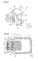
FIG. 8 is a sectional view taken along a line I-I ofFIG. 1 . -
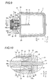
FIG. 9 is a sectional view taken along a line II-II ofFIG. 1 . -
FIG. 10 is an enlarged view of main parts shown inFIG. 9 . -
FIG. 11 is a perspective view of a CCD camera unit of the prior art. -
FIG. 12 is an enlarged view of main parts shown inFIG. 11 . - A
CCD camera unit 1, which is an electronic component according to an illustrative embodiment of the invention, will be described with reference toFIGS. 1 to 10 . - The
CCD camera unit 1 shown inFIGS. 1 and2 has a box-shaped camera case 2 having an opening, aconnection connector 3 that is assembled to thecamera case 2 to thus cover the opening, acircuit board 4 that is mounted to theconnection connector 3, a camera lens device (not shown) that is mounted on thecircuit board 4, at least one pair of (i.e., a plurality of)female terminals 7 serving as connection terminals that are connected to thecircuit board 4, afemale housing 5 serving as a housing that mounts the plurality offemale terminals 7 thereto, afirst packing 6, asecond packing 8 and arear holder 9 that is mounted to thefemale housing 5. - Also, an arrow Z shown in
FIG. 1 and the like indicates a direction along which thecircuit board 4 is introduced between the pair offemale terminals 7, i.e., a direction along which thecamera case 2 and theconnection connector 3 are assembled. An arrow X is indicative of a direction along which aspring member 72 of thefemale terminal 7 is elastically deformed. An arrow Y indicates a direction intersecting (orthogonal) with both the arrow Z and the arrow X. - The
camera case 2 is formed with arecess 22 into which a protrusion 34 (refer toFIG. 6 and the like) of the connection connector 3 (which will be described later) is fitted. Therecess 22 has a concave section from a surface of an edge of the opening of thecamera case 2 along the arrow Z direction. Also, therecess 22 is formed over an entire periphery of the edge of thecamera case 2. - The
connection connector 3 is made of insulating synthetic resin. Also, theconnection connector 3 has aplate section 31 covering the opening of thecamera case 2, and a plurality ofwall sections - The
plate section 31 is provided with the protrusion 34 (refer toFIG. 6 ) that is fitted into therecess 22 of thecamera case 2, and anopening 33 to which thecircuit board 4 is mounted. The opening 33 is provided at a central portion of theplate section 31 and penetrates theplate section 31. Also, thecircuit board 4 is press-fitted to an inside of theopening 33, so that thecircuit board 4 is mounted to theconnection connector 3. - The
protrusion 34 is formed in convex shape from a surface of theplate section 31 facing thecamera case 2. Theprotrusion 34 is fitted into therecess 22 of thecamera case 2, so that theconnection connector 3 is mounted to thecamera case 2. - The plurality of
wall sections plate section 31 in the arrow Z direction. Also, the plurality ofwall sections wall sections wall sections engaging sections 35 penetrating thewall sections engaging sections 35 are provided at central portions of therespective wall sections - The
circuit board 4 has a boardmain body 41, apress fitting section 42, which is provided to a side of the boardmain body 41 facing theconnection connector 3 in the arrow Z direction and has a width narrower than the boardmain body 41 in the arrow Y direction, and a plurality ofterminal sections 43 that is formed in convex shape from thepress fitting section 42 towards theconnection connector 3 in the arrow Z direction. Also, a surface of thecircuit board 4 is formed with awiring pattern 4a (refer toFIG. 10 ) that connects the camera lens device (not shown) and thefemale terminals 7 in a predetermined pattern. Thewiring pattern 4a is also formed on surfaces of therespective terminal sections 43. - The
press fitting section 42 is provided at a central portion of the boardmain body 41. Also, thepress fitting section 42 is press-fitted into the opening 33 of theconnection connector 3. - The plurality of
terminal sections 43 is arranged at an interval in the arrow Y direction. The respectiveterminal sections 43 are positioned between thespring members 72 of the pair offemale terminals 7, which will be described later. Also,ribs 57 of thefemale housing 5 serving as the housing are introduced between the plurality ofterminal sections 43 provided in the arrow Y direction. Also, positions of the respectiveterminal sections 43 in the arrow X direction are restrained between a pair ofrestraint sections 57b of thefemale housing 5, which will be described later. Also, when thepress fitting section 42 of thecircuit board 4 is press-fitted to theconnection connector 3, the plurality ofterminal sections 43 and a part of thepress fitting section 42 protrude from theplate section 31 of theconnection connector 3 in the arrow Z direction. - The
female terminal 7 is formed by punching or bending a conductive metal plate. As shown inFIGS. 3 and 4 , thefemale terminal 7 has integrally an electricwire connection section 71 and thespring member 72 serving as an electric contact section continuing from the electricwire connection section 71. Also, thefemale terminal 7 corresponds to the 'connection terminal' defined in the claims. - The electric
wire connection section 71 has integrally abottom plate 73 having a rectangular shape of a flat plate and a pair ofcore crimping pieces 74 provided to stand from both ends of thebottom plate 73 in a width direction (arrow Y direction). Also, a longitudinal direction (arrow Z direction) of the electricwire connection section 71 and a longitudinal direction (arrow Z direction) of anelectric wire 10 connected to the electricwire connection section 71 are parallel with each other. Also, theelectric wire 10 connected to the electricwire connection section 71 is bent to have an L shape and is thus held between holdingsections second packing 8, which will be described later. - The pair of
core crimping pieces 74 is bent so that edges distant from thebottom plate 73 become close to thebottom plate 73. The pair ofcore crimping pieces 74 holds a core, which is exposed as a sheath of theelectric wire 10 is stripped, between thebottom plate 73 and the core crimping pieces and thus crimps the core, so that thecore crimping pieces 74 and the core of theelectric wire 10 are electrically connected. - The
spring member 72 continues from thebottom plate 73. Also, an end of thespring member 72, which is distant from thebottom plate 73, is spirally bent in a direction in which therespective spring members 72 provided to the pair offemale terminals 7 come close to each other. Thereby, thespring member 72 is formed to be elastically deformable in the arrow X direction. - The
female housing 5 is made of insulating synthetic resin and has a substantially rectangular shape. Also, as shown inFIGS. 2 and5 , thefemale terminal 7 is mounted to thefemale housing 5 via thesecond packing 8. Thefemale housing 5 having thefemale terminals 7 mounted thereto is mounted to theconnection connector 3. When thefemale housing 5 is mounted to theconnection connector 3, thefemale terminals 7 mounted to thefemale housing 5 and thecircuit board 4 mounted to theconnection connector 3 are electrically connected. Thefemale housing 5 has a housingmain body 51, a pair ofprotrusions 52 provided to the housingmain body 51 andholder mounting sections 53 mounting arear holder 9. Also, thefemale housing 5 corresponds to the 'housing' defined in the claims. In the meantime,FIG. 5 shows thefemale housing 5 shown inFIG. 5 from theconnection connector 3. - The housing
main body 51 is provided with a plurality of through-holes 54 through which theelectric wires 10 and thefemale terminals 7 having theelectric wires 10 mounted thereto pass, a plurality ofcontact sections 55 provided on inner surfaces of the through-holes 54, asubstrate housing section 56 provided between the through-holes 54 in the arrow X direction, a plurality ofribs 57 provided between the plurality ofterminal sections 43 of thecircuit board 4, a firstpacking mounting section 58 to which thefirst packing 6 is mounted and a pair of sections to be engaged 59 each of which is engaged with each of the pair of engagingsections 35 of theconnection connector 3. Also, the housingmain body 51 is mounted between the plurality ofwall sections connection connector 3. - As shown in
FIG. 7 and10 , the through-holes 54 are arranged in a pair (two) in the arrow X direction and the three through-holes 54 are arranged in the arrow Y direction. Also, the through-holes 54 are provided at an interval each other. Also, each through-hole 54 penetrates the housingmain body 51 in the arrow Z direction. - The
contact sections 55 are provided at sides, which are distant from thecircuit board 4 in the arrow X direction of the pair ofspring members 72, and are provided in plural (pairs) at positions sandwiching the pair ofspring members 72 between the contact sections. That is, each pair ofcontact sections 55 is provided to face each other in a direction that the pair ofspring members 72 gets away from each other along the arrow X direction. Also, in the shown example, the plurality ofcontact sections 55 is provided in a pair (two) in the arrow X direction and the three contact sections are provided in the arrow Y direction. Also, thecontact sections 55 are provided on the inner surfaces of the through-holes 54 in the arrow X direction, and at end portions of the housingmain body 51 facing theconnection connector 3 in the arrow Z direction. The plurality (pairs) ofcontact sections 55 restrains thespring members 72 from moving in a direction getting away from thecircuit board 4 along the arrow X direction. - As shown in
FIGS. 6 and7 , thesubstrate housing section 56 has a shape that is concave from a surface of the housingmain body 51 facing theconnection connector 3 in the arrow Z direction, and houses theterminal sections 43 and a part of thepress fitting section 42 of thecircuit board 4, which protrude from theplate section 31 of theconnection connector 3. Also, thesubstrate housing section 56 extends in the arrow Y direction. Also, the plurality of through-holes 54a and thesubstrate housing section 56 communicate with each other. - The
ribs 57 protrude, along the arrow Z direction, frombottom sections 56a of thesubstrate housing section 56 in the arrow Z direction. Also, the plurality ofribs 57 is provided in the arrow Y direction so that side surfaces thereof face each other at an interval. Also, an end portion (i.e., end portion of therib 57 at the connection connector 3-side) of therib 57 distant from thebottom section 56a of thesubstrate housing section 56 in the arrow Z direction is positioned at an inner side (side distant from the connection connector 3) of a surface of the housingmain body 51 at the connection connector 3-side. Also, therib 57 is provided with a pair ofrestraint sections 57b protruding from the end portion of therib 57 towards thecircuit board 4 in the arrow Z direction. - The pair of
restraint sections 57b is provided at both end portions of therib 57 in the arrow X direction. The pair ofrestraint sections 57b restrains a position of thecircuit board 4 in the arrow X direction between the pair ofrestraint sections 57b. - The first
packing mounting section 58 has a shape that is recessed from the surface of the housingmain body 51 overlapping the plurality ofwall sections connection connector 3. Also, the firstpacking mounting section 58 is provided at an end portion of the housingmain body 51 facing theconnection connector 3 in the arrow Z direction. Also, the firstpacking mounting section 58 is provided over the entire periphery of the housingmain body 51. - The pair of sections to be engaged 59 is formed in convex shape from surfaces of the housing
main body 51, which overlap with thewall sections sections 35 provided thereon, towards directions getting away from each other along the arrow X direction. Also, each section to be engaged 59 is configured to be elastically deformable in the arrow X direction. Also, each section to be engaged 59 is provided between the firstpacking mounting section 59 and theprotrusion 52 that will be described later. - Each
protrusion 52 has a plate shape. Also, the pair ofprotrusions 52 is provided at end portions of the housingmain body 51 distant from theconnection connector 3 in the arrow Z direction. Also, the pair ofprotrusions 52 is formed in convex shape from the surfaces of the housingmain body 51 towards directions getting away from each other along the arrow X direction. Eachprotrusion 52 is provided over an entire length of the housingmain body 51 in the arrow Y direction. Also, eachprotrusion 52 continues from the housingmain body 51 at one end portion thereof in the arrow Z direction, and the other end portion of eachprotrusion 52 continues to aholder mounting section 53. Theprotrusions 52 contact thewall sections connection connector 3 at end portions thereof facing theconnection connector 3 in the arrow Z direction andcontact sidewall sections 92a, 92b of the rear holder 9 (which will be described later) at end portions thereof distant from theconnection connector 3 in the arrow Z direction. - The
holder mounting sections 53 are provided at end portions of thefemale housing 5 distant from theconnection connector 3 in the arrow Z direction. That is, theholder mounting sections 53 continue from the end portions of the housingmain body 51 distant from theconnection connector 3. Also, theholder mounting sections 53 are provided at both end portions of the housingmain body 51 in the arrow Y direction and are provided to stand from the end portions of the housingmain body 51 in the arrow Z direction. Also, theholder mounting sections 53 are provided over the entire length of the housingmain body 51 in the arrow X direction. Also, theholder mounting sections 53 are provided with engagingsections 50, respectively, which are engaged to therear holder 9. - A pair of the engaging
sections 50 is provided at end portions of theholder mounting sections 53 distant from theconnection connector 3 in the arrow Z direction. The pair of engagingsections 50 protrudes towards a direction along which the engaging sections get away from surfaces of theholder mounting sections 53. - The
first packing 6 has a frame shape and is made of synthetic resin having flexibility such as rubber, for example. Also, thefirst packing 6 is formed to be elastically deformable in both directions along which a diameter thereof is reduced (which means that inside and outside diameters are reduced) and the diameter is enlarged. Also, thefirst packing 6 is mounted to thefemale housing 5. When thefemale housing 5 is mounted to theconnection connector 3, thefirst packing 6 is positioned between thefemale housing 5 and theconnection connector 3, so that the first packing prevents liquid such as water from being introduced to thecircuit board 4. - The
second packing 8 is made of synthetic resin having flexibility such as rubber, for example. Also, as shown inFIGS. 3 and 4 , thesecond packing 8 is mounted to thefemale housing 5 with thefemale terminals 7 being mounted to thesecond packing 8, so that the second packing prevents the liquid such as water from being introduced into the through-holes 54 and thesubstrate housing section 56 of thefemale housing 5. Also, thesecond packing 8 has a pair of holdingsections electric wires 10 therebetween and a hinge 84 connecting the pair of holdingsections - The pair of holding
sections sections - The
holding section 8A has anopening 82 through which thefemale terminals 7 pass and placingportions 83 on which theelectric wires 10 are placed. Theopening 82 penetrates theholding section 8A in the arrow Z direction. Also, theopening 82 is provided at a central portion of theholding section 8A. The placingportions 83 are provided on the inner surface of theholding section 8A. Also, the plurality of (three, in the shown example) placingportions 83 is provided at an interval in the arrow Y direction. Each placingportion 83 is a recess that is concave from the inner surface of theholding section 8A and extends in the arrow X direction. Also, the placingportion 83 is provided with a plurality ofprotrusions 83a protruding from a bottom section of the concave shape of the placingportion 83. Theprotrusions 83a is provided at an interval. - The holding
section 8B is provided with placingportions 83 positioning theelectric wires 10 between the placing portions and the placingportions 83 of theholding section 8A. The placingportion 83 has a shape that is concave from the inner surface of the holdingsection 8B. - The
rear holder 9 includes a plate-shapedcover section 91 overlapping with the holdingsection 8B of thesecond packing 8 and a plurality ofsidewall sections cover section 91 towards thesecond packing 8 along the arrow Z direction, and has a cylindrical shape having a bottom. - Among the plurality of
sidewall sections sidewall sections 92a, 92b facing each other in the arrow X direction is provided with a plurality of notchedportions 93. The notchedportions 93 are notched in a concave shape from end portions of thesidewall sections 92a, 92b distant from thecover section 91 in the arrow Z direction towards thecover section 91. The notchedportions 93 are provided at positions corresponding to the placingportions 83 of thesecond packing 8 and are formed in plural (three, in the shown example) at an interval in the arrow Y direction. - Among the plurality of
sidewall sections sections 50 of thefemale housing 5, respectively. - The section to be engaged 94 has a pair of
slits 94a and ahole 94b provided between the pair ofslits 94a. The pair ofslits 94a is provided at an interval in the arrow X direction. Also, therespective slits 94a are linearly notched from end portions of thesidewall sections cover section 91 in the arrow Z direction, towards thecover section 91. Thehole 94b penetrates each of thesidewall sections slits 94a, so that the sections to be engaged is elastically deformable in the direction getting away from each other along the arrow Y direction. - The
CCD camera 1 is assembled as follows.
First, the core at the terminal of theelectric wire 10, which is exposed as the sheath of theelectric wire 10 is stripped, is placed on thebottom plate 73 of the electricwire connection section 71 of thefemale terminal 7 and thecore crimping piece 74 is crimped to approach thebottom plate 73. Thereby, thefemale terminal 7 is mounted to theelectric wire 10. Theelectric wires 10 having thefemale terminals 7 mounted thereto are made to pass through theopening 82 of theholding section 8A and are bent into the L shape, so that thefemale terminals 7 and theelectric wires 10 having thefemale terminals 7 mounted thereto are held between the placingportions 83 of the holdingsections second packing 8. By doing so, thefemale terminals 7 and theelectric wires 10 having thefemale terminals 7 mounted thereto are mounted to thesecond packing 8. Then, theelectric wires 10 and thefemale terminals 7 having thesecond packing 8 mounted thereto are made to pass through the through-holes 54 from theholder mounting sections 53 of thefemale housing 5, so that thesecond packing 8 is made to overlap with thefemale housing 5. After that, thecover section 91 of therear holder 9 is approached to overlap with the holdingsection 8B of thesecond packing 8. Thereby, the engagingsections 50 of thefemale housing 5 are engaged to the sections to be engaged 94 of therear holder 9. At this time, thesidewall sections 92a, 92b of therear holder 9 contact the pair ofprotrusions 52 of thefemale housing 5. Therear holder 9 is mounted to thefemale housing 5 as described above, so that theelectric wires 10 and thefemale terminals 7 are mounted to thefemale housing 5 via thesecond packing 8. - Then, the camera lens device (not shown) is connected to the
wiring pattern 4a of thecircuit board 4. By doing so, the camera lens device is mounted on thecircuit board 4. Thecircuit board 4 having the camera lens device mounted thereon is moved in the arrow Z direction to thus press-fit the press-fittingsection 42 of thecircuit board 4 into theopening 33 of theconnection connector 3, so that thecircuit board 4 is mounted to theconnection connector 3. - Then, the
first packing 6 is mounted to the firstpacking mounting section 58 of thefemale housing 5 having theelectric wires 10 and thefemale terminals 7 mounted thereto via thesecond packing 8. Then, thefemale housing 5 is made to come close to thewall sections connection connector 3. Thereby, the engagingsections 35 of theconnection connector 3 are engaged to the sections to be engaged 59 of thefemale housing 5. At this time, thewall sections connection connector 3 contact the pair ofprotrusions 52 of thefemale housing 5. Also, as shown inFIGS. 6 and7 , as thecircuit board 4 is moved (introduced) between the pair offemale terminals 7 in the arrow Z direction, eachterminal section 43 is introduced into thesubstrate housing section 56 of thefemale housing 5, and as shown inFIG. 8 , theribs 57 are introduced between theterminal sections 43 in the arrow Y direction and the pair ofspring members 72 positions eachterminal section 43 therebetween in the arrow X direction. By doing so, the pair ofspring members 72 elastically contacts thewiring pattern 4a formed on the respectiveterminal sections 43, so that the respectivefemale terminals 7 and thecircuit board 4 are electrically connected. At this time, as shown inFIGS. 9 and 10 , the pair ofspring members 72 is positioned between the pair ofcontact sections 55. Also, at this time, a position of thecircuit board 4 in the arrow X direction is restrained between the pair ofrestraint sections 57b of thefemale housing 5. Finally, theplate section 31 of theconnection connector 3 to which thefemale housing 5 having theelectric wires 10 and thefemale terminals 7 mounted thereto is mounted is approached to thus cover the opening of thecamera case 2. Thereby, theprotrusion 34 of theconnection connector 3 is fitted into therecess 22 of thecamera case 2, so that thecamera case 2 and theconnection connector 3 are mounted each other. By doing so, theCCD camera unit 1 is assembled. - According to the above illustrative embodiment, the
CCD camera unit 1 that is an electronic component includes thecircuit board 4, thefemale terminals 7 that are at least one pair of connection terminals connected to thecircuit board 4 and thefemale housing 5 that is the housing having the pair offemale terminals 7 mounted thereon. Thecircuit board 4 is provided with the plurality ofterminal sections 43 that is formed in convex shape towards thefemale housing 5, is provided at an interval and is connected to theconnection terminals 7. Each of the pair offemale terminals 7 is provided with thespring members 72 that are formed to be elastically deformable in both directions (arrow X direction) along which the pair offemale terminals 7 comes close to each other and gets away from each other and that sandwich theterminal sections 43 therebetween. Thefemale housing 5 is provided with at least onerib 57 that is provided between the through-holes 54 through which each of the pair offemale terminals 7 pass, that is formed in convex shape towards thecircuit board 4 from thebottom section 56a of thesubstrate housing section 56 in which thecircuit board 4 is housed and that is positioned between the plurality ofterminal sections 43. Therefore, for example, when theCCD camera unit 1 vibrates during the traveling of the vehicle, thespring members 72 are elastically deformed to thus apply the contact load to thecircuit board 4, so that the stable contact reliability between thecircuit board 4 and thefemale terminals 7 connected to thecircuit board 4 is maintained. Also, theribs 57 are provided, so that thecircuit board 4 is restrained from moving in the direction (arrow Y direction) intersecting (orthogonal) with both the direction (arrow X direction) along which thespring members 72 are elastically deformed and the direction (arrow Z direction) along which thecircuit board 4 is introduced between the pair offemale terminals 7. Thereby, the positional deviation between thefemale terminals 7 mounted to thefemale housing 5 and thecircuit board 4 is restrained. Therefore, even when theCCD camera 1 vibrates in the direction (arrow X direction) along which thespring members 72 are elastically deformed or in the intersecting (orthogonal) direction (arrow Y direction), the stable contact reliability between thecircuit board 4 and thefemale terminals 7 connected to thecircuit board 4 is maintained. Hence, it is possible to provide theCCD camera unit 1 in which the connected state between thecircuit board 4 and thefemale terminals 7 is favorably maintained. - Also, since the
spring members 72 provided to each of the pair offemale terminals 7 sandwich the terminal sections 43 (i.e., circuit board 4) therebetween, the pair ofspring members 72 and thecircuit board 4 overlap with each other. Thereby, it is possible to lower (i.e., miniaturize) the height of theCCD camera unit 1 in the direction (arrow Z direction) along which thecircuit board 4 is introduced between the pair offemale terminals 7. - Also, the
female housing 5 is provided with the pair ofcontact sections 55 that is provided in the direction along which the pair ofspring members 72 gets away from each other in the arrow X direction and that sandwiches the pair ofspring members 72 therebetween. Hence, thespring members 72 are brought into contact with thecontact sections 55, so that thespring members 72 are restrained from moving in the direction along which the spring members separate from thecircuit board 4. Thereby, it is possible to maintain the connected state between thecircuit board 4 and thefemale terminals 7 more favorably. - Also, the pair of
restraint sections 57b is provided which is formed in convex shape from therib 57 towards thecircuit board 4 and positions thecircuit board 4 therebetween. Thus, thecircuit board 4 is brought into contact with the pair ofrestraint sections 57b, so that thecircuit board 4 is restrained from moving in the direction (arrow X direction) along which thespring members 72 are elastically deformed. Thereby, the stable contact reliability between thecircuit board 4 and thefemale terminals 7 connected to thecircuit board 4 is maintained, so that it is possible to maintain the connected state between thecircuit board 4 and thefemale terminals 7 more favorably. - In the meantime, according to the above illustrative embodiment, the
press fitting section 42 of thecircuit board 4 is press-fitted into theopening 33 of theconnection connector 3, so that thecircuit board 4 is mounted to theconnection connector 3. However, the invention is not limited thereto. For example, thecircuit board 4 may be insert-molded to theconnection connector 3 and thus mounted thereto. - Also, according to the above illustrative embodiment, the plurality (pair) of
female terminals 7 serving as the connection terminals is provided. However, the invention is not limited thereto. For example, at least one pair offemale terminals 7 may be provided. - Also, according to the above illustrative embodiment, the plurality of
ribs 57 is provided. However, the invention is not limited thereto. For example, at least onerib 57 may be provided. - Also, the above illustrative embodiment shows a representative embodiment of the invention and the invention is not limited thereto. That is, a variety of modifications can be made without departing from the gist of the invention.
- This application is based on Japanese Patent Application No.
2010-093347 filed on April 14, 2010 - According to the electronic component of the invention, even when the electronic component vibrates during the traveling of the vehicle and even when the electronic component vibrates in the direction along which the spring members are elastically deformed or in the intersecting (orthogonal) direction, the stable contact reliability between the circuit board and the connection terminals connected to the circuit board is maintained. Thereby, it is possible to favorably maintain the connected state between the circuit board and the connection terminals.
-
- 1: CCD camera unit (electronic component)
- 4: circuit board
- 5: female housing (housing)
- 7: female terminal (connection terminal)
- 43: terminal section
- 54: through-hole
- 55: contact section
- 56: substrate housing section
- 56a: bottom section
- 57: rib
- 57b: restraint section
- 72: spring member
- Arrow X: direction along which a pair of spring members comes close to each other and get away from each other
Claims (3)
- An electronic component comprising:a circuit board;at least a pair of connection terminals connected to the circuit board; anda housing to which the pair of connection terminals are mounted,wherein the circuit board is provided with a plurality of terminal sections that are formed in convex shape towards the housing, provided at an interval and connected to the connection terminals,wherein each of the pair of connection terminals is provided with spring members that are formed to be elastically deformable in both directions along which the pair of connection terminals come close to each other and get away from each other and that sandwich the terminal sections therebetween,wherein the housing is provided with a substrate housing section that is disposed between through-holes through which the respective connection terminals pass and that houses the circuit board therein, andwherein the housing is provided with at least one rib that is formed in convex shape from a bottom section of the substrate housing section towards the circuit board and is introduced into the plurality of terminal sections.
- The electronic component according to claim 1, wherein the housing is provided with a pair of contact sections that is provided to face each other in the direction along which the pair of spring members get away from each other and that sandwich the pair of spring members therebetween.
- The electronic component according to claim 1 or 2, wherein a pair of restraint sections is provided which is formed in convex shape from the rib towards the circuit board and positions the circuit board therebetween.
Applications Claiming Priority (2)
| Application Number | Priority Date | Filing Date | Title |
|---|---|---|---|
| JP2010093347A JP5513232B2 (en) | 2010-04-14 | 2010-04-14 | Electronic components |
| PCT/JP2011/059099 WO2011129338A1 (en) | 2010-04-14 | 2011-04-12 | Electronic component |
Publications (2)
| Publication Number | Publication Date |
|---|---|
| EP2560242A1 true EP2560242A1 (en) | 2013-02-20 |
| EP2560242A4 EP2560242A4 (en) | 2014-03-05 |
Family
ID=44798709
Family Applications (1)
| Application Number | Title | Priority Date | Filing Date |
|---|---|---|---|
| EP11768859.8A Withdrawn EP2560242A4 (en) | 2010-04-14 | 2011-04-12 | ELECTRONIC COMPONENT |
Country Status (7)
| Country | Link |
|---|---|
| US (1) | US9161463B2 (en) |
| EP (1) | EP2560242A4 (en) |
| JP (1) | JP5513232B2 (en) |
| KR (1) | KR101397761B1 (en) |
| CN (1) | CN102859798B (en) |
| BR (1) | BR112012025555A2 (en) |
| WO (1) | WO2011129338A1 (en) |
Families Citing this family (17)
| Publication number | Priority date | Publication date | Assignee | Title |
|---|---|---|---|---|
| US9011177B2 (en) | 2009-01-30 | 2015-04-21 | Molex Incorporated | High speed bypass cable assembly |
| US9142921B2 (en) | 2013-02-27 | 2015-09-22 | Molex Incorporated | High speed bypass cable for use with backplanes |
| US9284198B2 (en) | 2013-06-28 | 2016-03-15 | Air Products And Chemicals, Inc. | Process for making trisilylamine |
| US20150042874A1 (en) * | 2013-08-08 | 2015-02-12 | Nidec Elesys Corporation | In-vehicle camera |
| WO2015035052A1 (en) * | 2013-09-04 | 2015-03-12 | Molex Incorporated | Connector system with cable by-pass |
| JP2016072456A (en) * | 2014-09-30 | 2016-05-09 | パナソニックIpマネジメント株式会社 | Outer shell structure of electronic equipment and terminal unit of load control system |
| USD780703S1 (en) * | 2014-10-20 | 2017-03-07 | S.J. Electro Systems, Inc. | Control panel cover |
| CN107112666B (en) | 2015-01-11 | 2019-04-23 | 莫列斯有限公司 | Board Connector Assemblies, Connectors and Bypass Cable Assemblies |
| TWI637568B (en) | 2015-01-11 | 2018-10-01 | 莫仕有限公司 | Circuit board bypass assembly and its components |
| DE112016002059B4 (en) | 2015-05-04 | 2026-05-13 | Molex, Llc | Computing device that uses a bypass unit |
| JP2017083756A (en) * | 2015-10-30 | 2017-05-18 | 日本圧着端子製造株式会社 | Imaging device |
| KR102450557B1 (en) * | 2015-11-12 | 2022-10-05 | 엘지이노텍 주식회사 | Camera module |
| KR102092627B1 (en) | 2016-01-11 | 2020-03-24 | 몰렉스 엘엘씨 | Route assembly and system using same |
| WO2017123614A1 (en) | 2016-01-11 | 2017-07-20 | Molex, Llc | Cable connector assembly |
| WO2017127513A1 (en) | 2016-01-19 | 2017-07-27 | Molex, Llc | Integrated routing assembly and system using same |
| US9985399B2 (en) * | 2016-02-03 | 2018-05-29 | Canon Kabushiki Kaisha | Accessory shoe device to which accessory is attached, image pickup apparatus, and accessory |
| CN112470555B (en) * | 2018-08-02 | 2022-03-22 | 三菱电机株式会社 | Electronic control device |
Family Cites Families (6)
| Publication number | Priority date | Publication date | Assignee | Title |
|---|---|---|---|---|
| US3629787A (en) * | 1970-06-19 | 1971-12-21 | Bell Telephone Labor Inc | Connector for flexible circuitry |
| JPS62123081U (en) | 1986-01-28 | 1987-08-05 | ||
| JP2002367696A (en) * | 2001-06-08 | 2002-12-20 | Sumitomo Wiring Syst Ltd | Card edge connector |
| JP5024945B2 (en) | 2007-10-17 | 2012-09-12 | 矢崎総業株式会社 | Contact connection structure |
| JP5239714B2 (en) | 2008-10-03 | 2013-07-17 | トヨタ自動車株式会社 | Wireless communication apparatus for vehicle and communication method |
| KR100913922B1 (en) * | 2009-02-02 | 2009-08-26 | 최상무 | Removable LED lighting device structure |
-
2010
- 2010-04-14 JP JP2010093347A patent/JP5513232B2/en not_active Expired - Fee Related
-
2011
- 2011-04-12 KR KR1020127026799A patent/KR101397761B1/en not_active Expired - Fee Related
- 2011-04-12 EP EP11768859.8A patent/EP2560242A4/en not_active Withdrawn
- 2011-04-12 US US13/636,723 patent/US9161463B2/en not_active Expired - Fee Related
- 2011-04-12 BR BR112012025555A patent/BR112012025555A2/en not_active IP Right Cessation
- 2011-04-12 WO PCT/JP2011/059099 patent/WO2011129338A1/en not_active Ceased
- 2011-04-12 CN CN201180019154.XA patent/CN102859798B/en not_active Expired - Fee Related
Also Published As
| Publication number | Publication date |
|---|---|
| KR20120130338A (en) | 2012-11-30 |
| WO2011129338A1 (en) | 2011-10-20 |
| JP2011222454A (en) | 2011-11-04 |
| US20130010443A1 (en) | 2013-01-10 |
| BR112012025555A2 (en) | 2016-06-28 |
| KR101397761B1 (en) | 2014-05-20 |
| CN102859798A (en) | 2013-01-02 |
| JP5513232B2 (en) | 2014-06-04 |
| US9161463B2 (en) | 2015-10-13 |
| CN102859798B (en) | 2016-03-09 |
| EP2560242A4 (en) | 2014-03-05 |
Similar Documents
| Publication | Publication Date | Title |
|---|---|---|
| US9161463B2 (en) | Electronic component | |
| KR101653437B1 (en) | Coaxial connector and method for assembling the same | |
| CN103427238B (en) | Electrical connector | |
| EP2736125A1 (en) | Component module, mating connector, and connection structure between component module and mating connector | |
| CN114204301B (en) | Plug connector, socket connector and electrical connector | |
| US8942007B2 (en) | Electrical component | |
| JP2014170726A (en) | Electric connector assembly and electric connector used for the same | |
| KR101110148B1 (en) | Press-fit contacts and electrical connectors using them | |
| JP4249192B2 (en) | Electrical equipment for module equipment | |
| JP2018085273A (en) | Contact, connector member, connector and connection target member | |
| JPH1141682A (en) | Microphone mounting device and mounting method | |
| WO2008001453A1 (en) | Coaxial cable connector | |
| JP2008171627A (en) | Female terminal fitting | |
| JP2008112682A (en) | Card edge type connector | |
| KR100710447B1 (en) | Plug Connector, Plug Contact, and Method for Assembling the Plug Connector | |
| CN220934443U (en) | Electrical connector | |
| JP6260643B2 (en) | Coaxial connector | |
| JP2021114397A (en) | connector | |
| JP2020095898A (en) | Harness component | |
| JP2003346946A (en) | Push-type connector | |
| JP2006092989A (en) | connector | |
| JP2017098013A (en) | Connector and connector manufacturing method |
Legal Events
| Date | Code | Title | Description |
|---|---|---|---|
| PUAI | Public reference made under article 153(3) epc to a published international application that has entered the european phase |
Free format text: ORIGINAL CODE: 0009012 |
|
| 17P | Request for examination filed |
Effective date: 20121015 |
|
| AK | Designated contracting states |
Kind code of ref document: A1 Designated state(s): AL AT BE BG CH CY CZ DE DK EE ES FI FR GB GR HR HU IE IS IT LI LT LU LV MC MK MT NL NO PL PT RO RS SE SI SK SM TR |
|
| DAX | Request for extension of the european patent (deleted) | ||
| A4 | Supplementary search report drawn up and despatched |
Effective date: 20140204 |
|
| RIC1 | Information provided on ipc code assigned before grant |
Ipc: H01L 27/148 20060101ALI20140129BHEP Ipc: H01R 13/05 20060101ALI20140129BHEP Ipc: H01L 27/146 20060101ALI20140129BHEP Ipc: H04N 5/225 20060101ALI20140129BHEP Ipc: H01R 12/77 20110101ALI20140129BHEP Ipc: H01L 27/14 20060101ALI20140129BHEP Ipc: H01R 12/71 20110101ALI20140129BHEP Ipc: H01R 12/72 20110101AFI20140129BHEP |
|
| 17Q | First examination report despatched |
Effective date: 20160715 |
|
| GRAP | Despatch of communication of intention to grant a patent |
Free format text: ORIGINAL CODE: EPIDOSNIGR1 |
|
| RIC1 | Information provided on ipc code assigned before grant |
Ipc: H01L 27/146 20060101ALI20170227BHEP Ipc: H01R 12/51 20110101ALN20170227BHEP Ipc: G03B 17/02 20060101ALN20170227BHEP Ipc: H05K 1/11 20060101AFI20170227BHEP Ipc: H01L 27/148 20060101ALI20170227BHEP Ipc: H04N 5/225 20060101ALI20170227BHEP Ipc: H01R 13/05 20060101ALI20170227BHEP Ipc: H01R 12/72 20110101ALI20170227BHEP Ipc: H05K 5/00 20060101ALI20170227BHEP |
|
| INTG | Intention to grant announced |
Effective date: 20170321 |
|
| STAA | Information on the status of an ep patent application or granted ep patent |
Free format text: STATUS: THE APPLICATION IS DEEMED TO BE WITHDRAWN |
|
| 18D | Application deemed to be withdrawn |
Effective date: 20170801 |