EP2560184B1 - Circuit breaker - Google Patents
Circuit breaker Download PDFInfo
- Publication number
- EP2560184B1 EP2560184B1 EP12172938.8A EP12172938A EP2560184B1 EP 2560184 B1 EP2560184 B1 EP 2560184B1 EP 12172938 A EP12172938 A EP 12172938A EP 2560184 B1 EP2560184 B1 EP 2560184B1
- Authority
- EP
- European Patent Office
- Prior art keywords
- bimetal
- pressing member
- cross bar
- coupling hole
- gap
- Prior art date
- Legal status (The legal status is an assumption and is not a legal conclusion. Google has not performed a legal analysis and makes no representation as to the accuracy of the status listed.)
- Active
Links
- 238000003825 pressing Methods 0.000 claims description 65
- 230000008878 coupling Effects 0.000 claims description 40
- 238000010168 coupling process Methods 0.000 claims description 40
- 238000005859 coupling reaction Methods 0.000 claims description 40
- 230000007246 mechanism Effects 0.000 claims description 23
- 238000000034 method Methods 0.000 claims description 22
- 230000003287 optical effect Effects 0.000 claims description 5
- 238000000926 separation method Methods 0.000 claims description 5
- 238000001514 detection method Methods 0.000 description 13
- 238000005452 bending Methods 0.000 description 10
- 238000003466 welding Methods 0.000 description 9
- 238000006073 displacement reaction Methods 0.000 description 7
- 238000001816 cooling Methods 0.000 description 6
- 230000008569 process Effects 0.000 description 4
- 238000004519 manufacturing process Methods 0.000 description 3
- 230000003247 decreasing effect Effects 0.000 description 2
- 239000011810 insulating material Substances 0.000 description 2
- 239000002184 metal Substances 0.000 description 2
- 229910052751 metal Inorganic materials 0.000 description 2
- 239000003973 paint Substances 0.000 description 2
- 230000002159 abnormal effect Effects 0.000 description 1
- 230000008859 change Effects 0.000 description 1
- 150000002739 metals Chemical class 0.000 description 1
- 238000012986 modification Methods 0.000 description 1
- 230000004048 modification Effects 0.000 description 1
- 230000002093 peripheral effect Effects 0.000 description 1
- 230000002265 prevention Effects 0.000 description 1
Images


Classifications
-
- H—ELECTRICITY
- H01—ELECTRIC ELEMENTS
- H01H—ELECTRIC SWITCHES; RELAYS; SELECTORS; EMERGENCY PROTECTIVE DEVICES
- H01H69/00—Apparatus or processes for the manufacture of emergency protective devices
- H01H69/01—Apparatus or processes for the manufacture of emergency protective devices for calibrating or setting of devices to function under predetermined conditions
-
- H—ELECTRICITY
- H01—ELECTRIC ELEMENTS
- H01H—ELECTRIC SWITCHES; RELAYS; SELECTORS; EMERGENCY PROTECTIVE DEVICES
- H01H71/00—Details of the protective switches or relays covered by groups H01H73/00 - H01H83/00
- H01H71/10—Operating or release mechanisms
- H01H71/12—Automatic release mechanisms with or without manual release
- H01H71/14—Electrothermal mechanisms
- H01H71/16—Electrothermal mechanisms with bimetal element
-
- H—ELECTRICITY
- H01—ELECTRIC ELEMENTS
- H01H—ELECTRIC SWITCHES; RELAYS; SELECTORS; EMERGENCY PROTECTIVE DEVICES
- H01H71/00—Details of the protective switches or relays covered by groups H01H73/00 - H01H83/00
- H01H71/10—Operating or release mechanisms
- H01H71/50—Manual reset mechanisms which may be also used for manual release
- H01H71/52—Manual reset mechanisms which may be also used for manual release actuated by lever
- H01H71/522—Manual reset mechanisms which may be also used for manual release actuated by lever comprising a cradle-mechanism
-
- H—ELECTRICITY
- H01—ELECTRIC ELEMENTS
- H01H—ELECTRIC SWITCHES; RELAYS; SELECTORS; EMERGENCY PROTECTIVE DEVICES
- H01H9/00—Details of switching devices, not covered by groups H01H1/00 - H01H7/00
- H01H9/30—Means for extinguishing or preventing arc between current-carrying parts
- H01H9/34—Stationary parts for restricting or subdividing the arc, e.g. barrier plate
Definitions
- the present disclosure relates to a method for controlling a gap in a circuit breaker including a detection mechanism having a structure for automatically setting a gap between a bimetal and a cross bar with respect to a time delay operating characteristic, the detection mechanism for detecting an accidental current and interrupting a circuit.
- a circuit breaker serves to open or close a load in an electric power substation or on an electrical circuit line, etc., or to interrupt a current when an accident such as a ground fault or a short-circuit current occurs.
- the circuit breaker converts a state of an electrical circuit into an 'OFF' or 'ON' state according to a user's manipulation. In the occurrence of an overload and a short-circuit current on the electrical circuit, the circuit breaker interrupts the circuit to protect the load and the electrical circuit.
- the circuit breaker has a time-limited trip characteristic and an instantaneous trip characteristic.
- the time-limited trip characteristic indicates an over-current trip characteristic having an operation time inversely-proportional to an over-current value.
- the time-limited trip characteristic includes a thermal magnetic type using a thermal factor such as bi-metal, and a hydraulic magnetic type using a breaking operation of an oil dash pot (ODP).
- the instantaneous trip characteristic is used to rapidly trip a circuit breaker by a large over-current such as a short-circuit current.
- the time-limited trip characteristic is used to trip a circuit breaker before the temperature of a wire reaches a dangerous state by Joule's heat, when an over-current more than a rated current flows on the wire.
- the time-limited trip characteristic It is advantageous for a circuit breaker to rapidly operate in the aspect of protection.
- an over-current such as an initial driving current of a motor, as well as a normal load current, flows on an electrical circuit.
- the circuit breaker preferably operates with time delay within a range that the temperature of the electrical circuit does not exceed an allowable temperature, so that the circuit breaker can be prevented from operating by the over-current. Therefore, the time-limited trip characteristic may be also referred to as a time delay operating characteristic.
- a factor which determines time delay in the time delay operating characteristic is a time duration from time when the bimetal starts to be bent due to an over-current, to time when the switching mechanism operates by rotation of the cross bar.
- Such time delay is determined based on an initial gap between a bimetal and a cross bar, a reactive bending amount from a time point when the bimetal comes in contact with the cross bar, to a time point when the cross bar rotates by a bending load of the bimetal, and a rotation distance of the cross bar until when the switching mechanism starts to operate upon rotation of the cross bar.
- a rotation degree of the bimetal i.e., a bending amount is determined based on the aforementioned factors.
- the reactive bending amount and the rotation distance of the cross bar are influenced by an individual characteristic of the circuit breaker. Therefore, it is difficult to minutely adjust the reactive bending amount and the rotation distance of the cross bar, unless the components are replaced.
- the only factor which determines time delay in the time delay operating characteristic is the gap between the bimetal and the cross bar.
- a trip time of the circuit breaker is shortened. This may cause the circuit to be interrupted even in a state of an over-current such as an initial driving current.
- the circuit breaker may have trip time delay, or may not be tripped. This may cause an over-current to be supplied to the circuit, resulting in damages of the circuit.
- the circuit breaker has a plurality of rated currents within the same structure. Therefore, when considering the number of types of bimetals and heaters, it is impossible to implement a constant gap and to satisfy the time delay operating characteristic with respect to an over-current in a single circuit breaker.
- the circuit breaker is categorized into several types based on the amount of heat generated from a heater and a bending amount of the bimetal when an over-current flows. And, the gap between the bimetal and the cross bar is adjusted when manufacturing the circuit breaker, for a precise time delay operating characteristic.
- the gap control is differently performed according to each rating, and is generally performed by an operator. More specifically, a contact gap between a screw and the cross bar is formed by controlling the height of the screw coupled to an upper part of the bimetal. To this end, the operator inserts a gap gauge between the cross bar and the screw, and rotates the screw so that the screw can be adhered to the gap gauge. Then, the operator removes the gap gauge, and fixes the screw to the cross bar.
- US 5,317,471 discloses a method of setting a bimetal strip in which a pin is adjusted before being secured by laser welding after the bimetal strip has reached a preset temperature.
- an objection obtainable with embodiments of the present invention is to provide a method for controlling a gap in a circuit breaker which includes a detection mechanism having a structure to facilitate automatically setting a gap between a bimetal and a cross bar, which is an important factor to determine a time delay operating characteristic of the circuit breaker.
- a riveting recess for riveting the pressing member may be formed at another end of the body portion, the end facing the separation preventing portion.
- the bimetal may be formed to be symmetrical on each side, right and left, with respect to the coupling hole.
- An identification means may be applied onto an upper part of the bimetal.
- the bimetal may have a shaving-processed upper part.
- Embodiments of the present invention may provide the following advantages.
- the gap between the pressing member and the cross bar may be controlled to be fixed in an automatic manner, not in a manual manner, so that productivity can be enhanced and cost can be saved.
- the gap between the pressing member and the cross bar can be controlled to be fixed in an automatic manner, not in a manual manner, so that the probability of error occurrence can be reduced, and thus the quality of the circuit breaker can be enhanced.
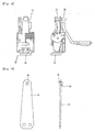
- FIG. 1 is a schematic view of a circuit breaker which may be used in accordance with the present invention.
- a circuit breaker 100 includes a case 10 configured to accommodate components therein.
- the case 10 is molded by an insulating material, and is configured to insulate the inside from the outside. Such structure is general, and thus its detailed explanations will be omitted.
- a switching mechanism 20 configured to turn on/off an electrical circuit
- a terminal part 50 including a fixed contactor 51 and a movable contactor 52 to which power and a load are connected, respectively
- a detection mechanism 30 configured to detect an abnormal current and an accidental current such as an over-current
- an extinguishing device 40 configured to extinguish an arc generated between contacts of the movable contactor 52 and the fixed contactor 51 when the electrical circuit was interrupted, etc.
- the terminal part 50 includes a fixed contactor 51 connected to an input side power and fixed to the case 10, and a movable contactor 52 connected to a load side, and rotatably mounted at the case 10 so as to contact or be separated from the fixed contactor 51.
- the movable contactor 52 is mechanically connected to the switching mechanism 20, and is manually driven by a lever. Alternatively, the movable contactor 52 is driven by the switching mechanism 20 operated by the detection mechanism 30.
- an arc which is in a high-temperature plasma state occurs because an insulated state in the air is not implemented any longer due to a current between the contacts. Furthermore, an arc pressure may occur due to gas generated as peripheral insulating materials, etc. are melted by the arc. Such arc is divided and cooled, and such arc pressure is discharged out by the extinguishing device 40.
- the detection mechanism 30 has a configuration to implement a time delay operation for interrupting a circuit when an over-current more than a rated current is detected. Such detection mechanism 30 is illustrated in FIGS. 4 and 8 in more details.
- the detection mechanism 30 includes a heater 34 configured to generate a proper amount of heat when an over-current occurs, a bimetal 31 connected to the heater 34 and bent to one side when receiving a proper amount of heat from the heater, a pressing member 32 protruding to be coupled to the end of the bimetal, and a cross bar 33 facing the bimetal in the protruding direction of the pressing member 32.
- the bimetal 31 is formed as two metals having different thermal expansion degrees come in contact with each other, and is bent to one side when receiving heat.
- FIG. 5 shows the bimetal 31 in more details
- FIG. 8 shows the bimetal 31 which is in a bent state.
- the bimetal 31 has a long rectangular plate shape.
- a coupling hole 35 for coupling a pressing member 32 to be later explained is provided at an upper part of the bimetal 31.
- a tap 36 for coupling the pressing member 32 to be later explained may be provided near the coupling hole 35.
- the bimetal 31 is formed to be symmetrical on each side, right and left, with respect to the coupling hole 35.
- An identification means may be applied onto an upper part of the bimetal 31.
- white paint may be applied to the upper part of the bimetal for facilitation of identification.
- An identification function may be implemented by an optical sensor so that the position of the bimetal can be easily checked.
- the bimetal may have a shaving-processed upper part.
- the shape and the processing of the bimetal 31 are implemented so as to precisely and automatically check the position of the bimetal using an optical sensor, for laser welding at the time of automatically adjusting a gap between the bimetal and a cross bar to be later explained.
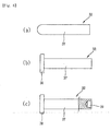
- FIGS. 6 and 7 show the pressing member 32 in more details
- FIG. 8 shows a process for coupling the pressing member 32 to the bimetal 31.
- FIG. 6 shows various embodiments of the pressing member 32.
- FIG. 6A shows a pressing member of a simple pillar shape.
- the pressing member 32 is provided with a pillar-shaped body portion 37 which penetrates through the coupling hole 35.
- One end of the pressing member 32 may undergo curved-surface processing for contact with a cross bar 33 to be later explained.
- the pressing member has a rivet shape.
- Such pressing member 32 includes a body portion 37 which penetrates through the coupling hole 35, and a separation preventing portion 38 formed at one end of the body portion, and having an outer diameter larger than the inner diameter of the coupling hole 35.
- the separation preventing portion 38 is formed at one end of the body portion 37, a side of the cross bar 33.
- an outer diameter of the body portion 37 of the pressing member is smaller than the inner diameter of the coupling hole 35.
- the reason is because the pressing member 32 should be initially coupled to the coupling hole 35 in a freely-movable state when automatically adjusting a gap between the bimetal and the cross bar.
- this is merely exemplary. After a gap (D) between the pressing member 32 and the cross bar 33 has been determined by apply of a prescribed current, the pressing member 32 is bonded to the coupling hole 35.
- a length (L2) of the body portion 37 is greater than an initial gap (L1) between the cross bar 33 and the bimetal 31. The reason is in order to prevent the pressing member from being separated from the coupling hole and the bimetal, sequentially, in an initial state where the pressing member has been coupled to the coupling hole of the bimetal so as to be freely-movable.
- a riveting recess 39 for riveting the pressing member may be formed at another end of the body portion 37. Said another end indicates the end of the body portion opposite to the one cross bar-side end of the body portion. Under this structure, the pressing member is coupled to the coupling hole, and then is riveted at the riveting recess. This can prevent the pressing member from being separated from the coupling hole and the bimetal, sequentially.
- the cross bar 33 mounted to the case 10 so as to face the bimetal 31 is spaced from the pressing member 32 by a prescribed gap (D), the pressing member 32 coupled to an upper part of the bimetal 31.
- D a prescribed gap
- the cross bar 33 is interworked with the aforementioned switching mechanism 20. That is, as the switching mechanism 20 operates by rotation of the cross bar 33, the movable contactor 52 is separated from the fixed contactor 51.
- the cross bar 33 After the cross bar 33 has come in contact with the pressing member 32, the cross bar 33 is pressed by bending of the bimetal 31. As a result, the cross bar has a rotational force to operate the switching mechanism.
- FIG. 2 A method for forming a gap in a circuit breaker according to an embodiment of the present invention is illustrated in FIG. 2 .
- the method includes a trip stroke measuring step (S50), a gap forming step (S100), a gap fixing step (S200), and a cooling step (S300).
- the trip stroke measuring step (S50) indicates a pre-step of forming a gap (D) between the pressing member coupled to the upper part of the bimetal and the cross bar.
- S50 the degree of a rotation displacement required to separate the movable contactor 52 from the fixed contactor 51 is measured.
- the rotation displacement of the cross bar has a reference value.
- Such reference value is required for automation in the process of production, which is predetermined according to each rating applied to the circuit breaker.
- the gap forming step (S100) indicates a step of bending the bimetal 31 by apply of a set current, in a state where the pressing member 32 has been coupled to the coupling hole 35 so as to be freely-movable, the coupling hole 35 formed at the upper part of the bimetal.
- FIG. 8 illustrates applications of the gap forming step (S100).
- the gap forming step (S100) includes an adhering step (S110) and a current applying step (S120).
- the adhering step (S110) indicates a step of adhering (closely attaching) the pressing member to the cross bar in a state where the pressing member 32 has been coupled to the coupling hole 35 so as to be freely-movable, the coupling hole 35 formed at the upper part of the bimetal.
- the current applying step (S120) indicates a step of bending the bimetal by apply of a set current for a set time, and thus relatively moving the pressing member to the bimetal in a state where the pressing member has been adhered to the cross bar.
- the pressing member 32 is adhered to the cross bar in a state where the pressing member 32 has been coupled to the coupling hole 35 so as to be freely-movable, the coupling hole 35 formed at the upper part of the bimetal. That is, the pressing member 32 is not fixedly-coupled to the bimetal 31.
- the bimetal is bent by apply of a set current for a set time.
- the pressing member is relatively moved toward the bimetal in a state of being adhered to the cross bar.
- the set time is required for automation in the process of production, which is predetermined according to each rating applied to the circuit breaker.
- the set current indicates a current determined with consideration of a rotation displacement of the cross bar measured in S50. Since the set current is an over-current, it has a numeric value where a time delay operating characteristic can be exhibited. If the rotation displacement of the cross bar exceeds a reference value, a set current applied to form the gap (D) between the pressing member coupled to the upper part of the bimetal and the cross bar is decreased. On the other hand, if the rotation displacement of the cross bar is less than the reference value, the set current is increased.
- the gap (D) is formed by relatively moving the pressing member 32 toward the bimetal 31 in a state where the pressing member 32 has been adhered to the cross bar.
- FIG. 8C illustrates a state after the pressing member has been fixed to the bimetal, which shows the gap (D) between the end of the pressing member 32 and the cross bar 33.
- the gap fixing step (S200) indicates a step of interrupting the set current, and of welding the pressing member 32 to the bimetal 31 when a set time has lapsed.
- the gap fixing step (S200) includes a current interrupting step (S210) and a welding step (S220).
- S210 is a step of interrupting the set current when a set time has lapsed.
- S220 is a step of coupling the pressing member, by welding, to the coupling hole formed at the upper part of the bimetal.
- the current interrupting step S210 indicates a step of making the gap (D) have no change, by interrupting the set current when a set time has lapsed, and by stopping a relative movement of the pressing member 32 toward the bimetal 31 in the state of FIG. 8B .
- the welding step S220 indicates a step of coupling the pressing member 32, by welding, to the coupling hole 35 formed at the upper part of the bimetal. That is, S220 indicates a step of fixing the gap (D) in the state of FIG. 8B .
- S220 laser welding is automatically performed.
- S220 a bending position of the bimetal is checked by a reflection-type optical sensor, and laser welding is performed.
- the bimetal 31 is formed to be symmetrical on each side, right and left, with respect to the coupling hole 35.
- An identification means is applied onto an upper part of the bimetal 31, and the bimetal 31 has a shaving-processed upper part. For instance, white paint may be applied on the upper part of the bimetal for facilitation of identification.
- Such configurations are implemented in order to precisely and automatically check the position of the bimetal using an optical sensor.
- FIG. 8C illustrates a detection mechanism cooled in the cooling step (S300),
- the cooling step (S300) indicates a step of cooling the heated bimetal 31 and the pressing member 32 after the gap fixing step.
- a natural cooling method or other cooling methods may be used.
- FIG. 3 is a flowchart showing a method for controlling a gap in a circuit breaker according to another embodiment of the present invention.
- the method may further include a riveting step (S70) of riveting the end of the pressing member so that the pressing member 32 can be prevented from being separated from the coupling hole 35 of the bimetal.
- S70 may be performed before S100.
- the pressing member Before S100, the pressing member may be separated from the coupling hole 35 of the bimetal since it is in a state of being freely-movable in the coupling hole 35. To prevent this, riveting is performed at the riveting recess 39 formed at another end of the body portion 37 of the pressing member 32.
- S70 may be performed after the gap (D) has been fixed in the gap fixing step (S200).
Description
- The present disclosure relates to a method for controlling a gap in a circuit breaker including a detection mechanism having a structure for automatically setting a gap between a bimetal and a cross bar with respect to a time delay operating characteristic, the detection mechanism for detecting an accidental current and interrupting a circuit.
- A circuit breaker serves to open or close a load in an electric power substation or on an electrical circuit line, etc., or to interrupt a current when an accident such as a ground fault or a short-circuit current occurs. The circuit breaker converts a state of an electrical circuit into an 'OFF' or 'ON' state according to a user's manipulation. In the occurrence of an overload and a short-circuit current on the electrical circuit, the circuit breaker interrupts the circuit to protect the load and the electrical circuit.
- The circuit breaker has a time-limited trip characteristic and an instantaneous trip characteristic. The time-limited trip characteristic indicates an over-current trip characteristic having an operation time inversely-proportional to an over-current value. And, the time-limited trip characteristic includes a thermal magnetic type using a thermal factor such as bi-metal, and a hydraulic magnetic type using a breaking operation of an oil dash pot (ODP).
- The instantaneous trip characteristic is used to rapidly trip a circuit breaker by a large over-current such as a short-circuit current. And, the time-limited trip characteristic is used to trip a circuit breaker before the temperature of a wire reaches a dangerous state by Joule's heat, when an over-current more than a rated current flows on the wire.
- Hereinafter, the time-limited trip characteristic will be explained. It is advantageous for a circuit breaker to rapidly operate in the aspect of protection. However, an over-current such as an initial driving current of a motor, as well as a normal load current, flows on an electrical circuit. Accordingly, the circuit breaker preferably operates with time delay within a range that the temperature of the electrical circuit does not exceed an allowable temperature, so that the circuit breaker can be prevented from operating by the over-current. Therefore, the time-limited trip characteristic may be also referred to as a time delay operating characteristic.
- Once an over-current is applied to the circuit breaker, heat is generated from a heater. Such generated heat is conducted to a bimetal to cause the bimetal to be bent due to a thermal conduction difference between two members of the bimetal. As the bimetal is bent, a cross bar is pressed to be rotated. As a result, a switching mechanism operates to convert a state of the electrical circuit into an open state, thereby interrupting the circuit.
- A factor which determines time delay in the time delay operating characteristic is a time duration from time when the bimetal starts to be bent due to an over-current, to time when the switching mechanism operates by rotation of the cross bar. Such time delay is determined based on an initial gap between a bimetal and a cross bar, a reactive bending amount from a time point when the bimetal comes in contact with the cross bar, to a time point when the cross bar rotates by a bending load of the bimetal, and a rotation distance of the cross bar until when the switching mechanism starts to operate upon rotation of the cross bar.
- A rotation degree of the bimetal, i.e., a bending amount is determined based on the aforementioned factors. The reactive bending amount and the rotation distance of the cross bar are influenced by an individual characteristic of the circuit breaker. Therefore, it is difficult to minutely adjust the reactive bending amount and the rotation distance of the cross bar, unless the components are replaced. As a result, the only factor which determines time delay in the time delay operating characteristic is the gap between the bimetal and the cross bar.
- If the gap between the bimetal and the cross bar is too small, a trip time of the circuit breaker is shortened. This may cause the circuit to be interrupted even in a state of an over-current such as an initial driving current. On the contrary, if the gap between the bimetal and the cross bar is too large, the circuit breaker may have trip time delay, or may not be tripped. This may cause an over-current to be supplied to the circuit, resulting in damages of the circuit.
- Generally, the circuit breaker has a plurality of rated currents within the same structure. Therefore, when considering the number of types of bimetals and heaters, it is impossible to implement a constant gap and to satisfy the time delay operating characteristic with respect to an over-current in a single circuit breaker.
- Generally, the circuit breaker is categorized into several types based on the amount of heat generated from a heater and a bending amount of the bimetal when an over-current flows. And, the gap between the bimetal and the cross bar is adjusted when manufacturing the circuit breaker, for a precise time delay operating characteristic.
- The gap control is differently performed according to each rating, and is generally performed by an operator. More specifically, a contact gap between a screw and the cross bar is formed by controlling the height of the screw coupled to an upper part of the bimetal. To this end, the operator inserts a gap gauge between the cross bar and the screw, and rotates the screw so that the screw can be adhered to the gap gauge. Then, the operator removes the gap gauge, and fixes the screw to the cross bar.
- Generally, it is necessary to minutely control the gap within the range of 0.1 mm. However, since the aforementioned gap control is manually performed, an error occurs according to each operator. Furthermore, even if the same operator performs the gap control, an error may occur according to each product. The time delay operating characteristic of the circuit breaker may be influenced by such error, and thus the quality of the circuit breaker may be lowered.
- Furthermore, if the process is manually performed, it takes a lot of time to perform the gap control. This may lower the productivity.
-
DE 84 16 195 U1 discloses a bimetal thermal overcurrent switch. -
US 5,317,471 discloses a method of setting a bimetal strip in which a pin is adjusted before being secured by laser welding after the bimetal strip has reached a preset temperature. - Therefore, an objection obtainable with embodiments of the present invention is to provide a method for controlling a gap in a circuit breaker which includes a detection mechanism having a structure to facilitate automatically setting a gap between a bimetal and a cross bar, which is an important factor to determine a time delay operating characteristic of the circuit breaker.
- According to the present invention, there is provided a method for forming a gap in a circuit breaker according to
claim 1. - A riveting recess for riveting the pressing member may be formed at another end of the body portion, the end facing the separation preventing portion.
- The bimetal may be formed to be symmetrical on each side, right and left, with respect to the coupling hole. An identification means may be applied onto an upper part of the bimetal. The bimetal may have a shaving-processed upper part.
- Embodiments of the present invention may provide the following advantages.
- Firstly, the gap between the pressing member and the cross bar may be controlled to be fixed in an automatic manner, not in a manual manner, so that productivity can be enhanced and cost can be saved.
- Secondly, the gap between the pressing member and the cross bar can be controlled to be fixed in an automatic manner, not in a manual manner, so that the probability of error occurrence can be reduced, and thus the quality of the circuit breaker can be enhanced.
- Further scope of applicability of the present invention will become more apparent from the detailed description given hereinafter. However, it should be understood that the detailed description and specific examples, while indicating preferred embodiments of the invention, are given by way of illustration only, since various changes and modifications within the scope of the appended claims will become apparent to those skilled in the art from the detailed description.
- The accompanying drawings, which are included to provide a further understanding of the invention and are incorporated in and constitute a part of this specification, illustrate exemplary embodiments and together with the description serve to explain the principles of the invention.
- In the drawings:
-
FIG. 1 is a schematic view of a circuit breaker which may be used in accordance with the present invention; -
FIG. 2 is a flowchart showing a method for controlling a gap in a circuit breaker according to an embodiment of the present invention; -
FIG. 3 is a flowchart showing a method for controlling a gap in a circuit breaker according to another embodiment of the present invention; -
FIG. 4 shows a front view and a side view of a detection mechanism of a circuit breaker which may be used in embodiments of the method according to the present invention; -
FIG. 5 shows a front view and a side view of a bimetal of the detection mechanism ofFIG. 4 ; -
FIG. 6 is a schematic view showing various embodiments of a pressing member of the detection mechanism ofFIG. 4 ; -
FIG. 7 is a schematic view showing positions of a pressing member and a cross bar, and a gap therebetween; and -
FIG. 8 is a schematic view showing a state of a detection mechanism, the state controlled by a method for controlling a gap in a circuit breaker according to an embodiment of the present invention. - Description will now be given in detail of the exemplary embodiments, with reference to the accompanying drawings. For the sake of brief description with reference to the drawings, the same or equivalent components will be provided with the same reference numbers, and description thereof will not be repeated.
-
FIG. 1 is a schematic view of a circuit breaker which may be used in accordance with the present invention. - Referring to
FIG. 1 , acircuit breaker 100 includes acase 10 configured to accommodate components therein. Thecase 10 is molded by an insulating material, and is configured to insulate the inside from the outside. Such structure is general, and thus its detailed explanations will be omitted. - In the
case 10, provided are aswitching mechanism 20 configured to turn on/off an electrical circuit, aterminal part 50 including a fixedcontactor 51 and amovable contactor 52 to which power and a load are connected, respectively, adetection mechanism 30 configured to detect an abnormal current and an accidental current such as an over-current, an extinguishingdevice 40 configured to extinguish an arc generated between contacts of themovable contactor 52 and the fixedcontactor 51 when the electrical circuit was interrupted, etc. - The
terminal part 50 includes a fixedcontactor 51 connected to an input side power and fixed to thecase 10, and amovable contactor 52 connected to a load side, and rotatably mounted at thecase 10 so as to contact or be separated from the fixedcontactor 51. - The
movable contactor 52 is mechanically connected to theswitching mechanism 20, and is manually driven by a lever. Alternatively, themovable contactor 52 is driven by theswitching mechanism 20 operated by thedetection mechanism 30. - In case of protecting the circuit through a tripping operation by separating the
movable contactor 52 from the fixedcontactor 51 in the occurrence of an accidental current, an arc which is in a high-temperature plasma state occurs because an insulated state in the air is not implemented any longer due to a current between the contacts. Furthermore, an arc pressure may occur due to gas generated as peripheral insulating materials, etc. are melted by the arc. Such arc is divided and cooled, and such arc pressure is discharged out by the extinguishingdevice 40. - The
detection mechanism 30 has a configuration to implement a time delay operation for interrupting a circuit when an over-current more than a rated current is detected.Such detection mechanism 30 is illustrated inFIGS. 4 and8 in more details. - Referring to
FIGS. 4 and8 , thedetection mechanism 30 includes aheater 34 configured to generate a proper amount of heat when an over-current occurs, a bimetal 31 connected to theheater 34 and bent to one side when receiving a proper amount of heat from the heater, a pressingmember 32 protruding to be coupled to the end of the bimetal, and across bar 33 facing the bimetal in the protruding direction of the pressingmember 32. - The bimetal 31 is formed as two metals having different thermal expansion degrees come in contact with each other, and is bent to one side when receiving heat.
-
FIG. 5 shows the bimetal 31 in more details, andFIG. 8 shows the bimetal 31 which is in a bent state. - Referring to
FIG. 5 , the bimetal 31 has a long rectangular plate shape. Acoupling hole 35 for coupling a pressingmember 32 to be later explained is provided at an upper part of the bimetal 31. Atap 36 for coupling the pressingmember 32 to be later explained may be provided near thecoupling hole 35. - The bimetal 31 is formed to be symmetrical on each side, right and left, with respect to the
coupling hole 35. An identification means may be applied onto an upper part of the bimetal 31. For instance, white paint may be applied to the upper part of the bimetal for facilitation of identification. However, the present invention is not limited to this. An identification function may be implemented by an optical sensor so that the position of the bimetal can be easily checked. - The bimetal may have a shaving-processed upper part. The shape and the processing of the bimetal 31 are implemented so as to precisely and automatically check the position of the bimetal using an optical sensor, for laser welding at the time of automatically adjusting a gap between the bimetal and a cross bar to be later explained.
-
FIGS. 6 and7 show the pressingmember 32 in more details, andFIG. 8 shows a process for coupling the pressingmember 32 to the bimetal 31. Especially,FIG. 6 shows various embodiments of the pressingmember 32. - The pressing
member 32 coupled to thecoupling hole 35 formed at the upper part of the bimetal 31 has various embodiments as shown inFIG. 6. FIG. 6A shows a pressing member of a simple pillar shape. In this case, the pressingmember 32 is provided with a pillar-shapedbody portion 37 which penetrates through thecoupling hole 35. One end of the pressingmember 32 may undergo curved-surface processing for contact with across bar 33 to be later explained. - Referring to
FIG. 6B , the pressing member has a rivet shape. Such pressingmember 32 includes abody portion 37 which penetrates through thecoupling hole 35, and aseparation preventing portion 38 formed at one end of the body portion, and having an outer diameter larger than the inner diameter of thecoupling hole 35. Here, theseparation preventing portion 38 is formed at one end of thebody portion 37, a side of thecross bar 33. - Referring to
FIGS. 6A and 6B , an outer diameter of thebody portion 37 of the pressing member is smaller than the inner diameter of thecoupling hole 35. The reason is because the pressingmember 32 should be initially coupled to thecoupling hole 35 in a freely-movable state when automatically adjusting a gap between the bimetal and the cross bar. However, this is merely exemplary. After a gap (D) between the pressingmember 32 and thecross bar 33 has been determined by apply of a prescribed current, the pressingmember 32 is bonded to thecoupling hole 35. - As shown in
FIG. 7 , a length (L2) of thebody portion 37 is greater than an initial gap (L1) between thecross bar 33 and the bimetal 31. The reason is in order to prevent the pressing member from being separated from the coupling hole and the bimetal, sequentially, in an initial state where the pressing member has been coupled to the coupling hole of the bimetal so as to be freely-movable. - Referring to
FIG. 6C , ariveting recess 39 for riveting the pressing member may be formed at another end of thebody portion 37. Said another end indicates the end of the body portion opposite to the one cross bar-side end of the body portion. Under this structure, the pressing member is coupled to the coupling hole, and then is riveted at the riveting recess. This can prevent the pressing member from being separated from the coupling hole and the bimetal, sequentially. - The
cross bar 33 mounted to thecase 10 so as to face the bimetal 31 is spaced from the pressingmember 32 by a prescribed gap (D), the pressingmember 32 coupled to an upper part of the bimetal 31. Such state indicates a state after the pressing member has been welded to the bimetal for prevention of free moving. - The
cross bar 33 is interworked with theaforementioned switching mechanism 20. That is, as theswitching mechanism 20 operates by rotation of thecross bar 33, themovable contactor 52 is separated from the fixedcontactor 51. - After the
cross bar 33 has come in contact with the pressingmember 32, thecross bar 33 is pressed by bending of the bimetal 31. As a result, the cross bar has a rotational force to operate the switching mechanism. - A method for forming a gap in a circuit breaker according to an embodiment of the present invention is illustrated in
FIG. 2 . Referring toFIG. 2 , the method includes a trip stroke measuring step (S50), a gap forming step (S100), a gap fixing step (S200), and a cooling step (S300). - The trip stroke measuring step (S50) indicates a pre-step of forming a gap (D) between the pressing member coupled to the upper part of the bimetal and the cross bar. In S50, the degree of a rotation displacement required to separate the
movable contactor 52 from the fixedcontactor 51 is measured. - The rotation displacement of the cross bar has a reference value. Such reference value is required for automation in the process of production, which is predetermined according to each rating applied to the circuit breaker.
- If the rotation displacement of the cross bar measured in S50 exceeds the reference value, a set current applied to form the gap (D) between the bimetal and the cross bar is decreased. On the other hand, if the rotation displacement of the cross bar measured in S50 is less than the reference value, the set current is increased.
- The gap forming step (S100) indicates a step of bending the bimetal 31 by apply of a set current, in a state where the pressing
member 32 has been coupled to thecoupling hole 35 so as to be freely-movable, thecoupling hole 35 formed at the upper part of the bimetal.FIG. 8 illustrates applications of the gap forming step (S100). - Referring to
FIGS. 2 and8 , the gap forming step (S100) includes an adhering step (S110) and a current applying step (S120). The adhering step (S110) indicates a step of adhering (closely attaching) the pressing member to the cross bar in a state where the pressingmember 32 has been coupled to thecoupling hole 35 so as to be freely-movable, thecoupling hole 35 formed at the upper part of the bimetal. And, the current applying step (S120) indicates a step of bending the bimetal by apply of a set current for a set time, and thus relatively moving the pressing member to the bimetal in a state where the pressing member has been adhered to the cross bar. - As shown in
FIG. 8A , in S110, the pressingmember 32 is adhered to the cross bar in a state where the pressingmember 32 has been coupled to thecoupling hole 35 so as to be freely-movable, thecoupling hole 35 formed at the upper part of the bimetal. That is, the pressingmember 32 is not fixedly-coupled to the bimetal 31. - As shown in
FIG. 8B , in S120, the bimetal is bent by apply of a set current for a set time. As a result, the pressing member is relatively moved toward the bimetal in a state of being adhered to the cross bar. Here, the set time is required for automation in the process of production, which is predetermined according to each rating applied to the circuit breaker. - As aforementioned, the set current indicates a current determined with consideration of a rotation displacement of the cross bar measured in S50. Since the set current is an over-current, it has a numeric value where a time delay operating characteristic can be exhibited. If the rotation displacement of the cross bar exceeds a reference value, a set current applied to form the gap (D) between the pressing member coupled to the upper part of the bimetal and the cross bar is decreased. On the other hand, if the rotation displacement of the cross bar is less than the reference value, the set current is increased.
- The gap (D) is formed by relatively moving the pressing
member 32 toward the bimetal 31 in a state where the pressingmember 32 has been adhered to the cross bar. -
FIG. 8C illustrates a state after the pressing member has been fixed to the bimetal, which shows the gap (D) between the end of the pressingmember 32 and thecross bar 33. - The gap fixing step (S200) indicates a step of interrupting the set current, and of welding the pressing
member 32 to the bimetal 31 when a set time has lapsed. - Referring to
FIG. 2 , the gap fixing step (S200) includes a current interrupting step (S210) and a welding step (S220). S210 is a step of interrupting the set current when a set time has lapsed. And, S220 is a step of coupling the pressing member, by welding, to the coupling hole formed at the upper part of the bimetal. - The current interrupting step S210 indicates a step of making the gap (D) have no change, by interrupting the set current when a set time has lapsed, and by stopping a relative movement of the pressing
member 32 toward the bimetal 31 in the state ofFIG. 8B . - The welding step S220 indicates a step of coupling the pressing
member 32, by welding, to thecoupling hole 35 formed at the upper part of the bimetal. That is, S220 indicates a step of fixing the gap (D) in the state ofFIG. 8B . - In S220, laser welding is automatically performed. In S220, a bending position of the bimetal is checked by a reflection-type optical sensor, and laser welding is performed.
- More specifically, the bimetal 31 is formed to be symmetrical on each side, right and left, with respect to the
coupling hole 35. An identification means is applied onto an upper part of the bimetal 31, and the bimetal 31 has a shaving-processed upper part. For instance, white paint may be applied on the upper part of the bimetal for facilitation of identification. Such configurations are implemented in order to precisely and automatically check the position of the bimetal using an optical sensor. -
FIG. 8C illustrates a detection mechanism cooled in the cooling step (S300), The cooling step (S300) indicates a step of cooling theheated bimetal 31 and the pressingmember 32 after the gap fixing step. In S300, a natural cooling method or other cooling methods may be used. -
FIG. 3 is a flowchart showing a method for controlling a gap in a circuit breaker according to another embodiment of the present invention. - The method may further include a riveting step (S70) of riveting the end of the pressing member so that the pressing
member 32 can be prevented from being separated from thecoupling hole 35 of the bimetal. - Referring to
FIG. 3 , S70 may be performed before S100. Before S100, the pressing member may be separated from thecoupling hole 35 of the bimetal since it is in a state of being freely-movable in thecoupling hole 35. To prevent this, riveting is performed at theriveting recess 39 formed at another end of thebody portion 37 of the pressingmember 32. S70 may be performed after the gap (D) has been fixed in the gap fixing step (S200).
Claims (5)
- A method for forming a gap in a circuit breaker, the circuit breaker (100), comprising:a fixed contactor (51) configured to receive power from an electrical circuit and to supply the power to a load side;a movable contactor (52) configured to open or close a circuit by contacting or being separated from the fixed contactor (51);a bimetal (31) arranged to be bent by heat generated from a conductive current;a pressing member (32) coupled to an upper part of the bimetal (31);a cross bar (33) spaced from the pressing member (32) by a prescribed gap, and configured to contact the pressing member (32) and to rotate by being pressed when the bimetal (31) is bent; anda switching mechanism (20) arranged to be operated by rotation of the cross bar (33), and configured to separate the movable contactor (52) from the fixed contactor (51);wherein a coupling hole (35) for coupling the pressing member (32) is provided at an upper part of the bimetal (31); andwherein the pressing member (32) includes:a body portion (37) which penetrates through the coupling hole (35); characterised in that the pressing member (32) is formed to have a rivet shape, andwherein a separation preventing portion (38) is formed at one cross bar-side end of the body portion (37), and has an outer diameter larger than the inner diameter of the coupling hole (35), andwherein an outer diameter of the body portion (37) is smaller than the inner diameter of the coupling hole (35); andwherein a length (L2) of the body portion (37) is greater than a gap (L1) between the cross bar (33) and the bimetal (31) when no current has been applied to bend the bimetal,the method comprising bonding the pressing member (32) to the coupling hole (35) after a prescribed gap (D) between the pressing member and the cross bar (33) has been formed by applying a set current for a set time to the bimetal when the pressing member (32) is in a state of being freely movable in the coupling hole (35).
- The method of Claim 1, wherein a riveting recess (39) for riveting the pressing member (32) is formed at another end of the body portion (37), being the end opposite to that at which the separation preventing portion (38) is formed.
- The method of one of Claims 1 or 2, wherein the bimetal (31) is formed to be symmetrical on each side, right and left, with respect to the coupling hole (35).
- The method of one of Claims 1 to 3, wherein an identification means is applied onto an upper part of the bimetal (31) to facilitate an identification function implemented by an optical sensor to check the position of the bimetal.
- The method of one of Claims 1 to 4, wherein the bimetal (31) has a shaving-processed upper part.
Applications Claiming Priority (1)
| Application Number | Priority Date | Filing Date | Title |
|---|---|---|---|
| KR1020110061955A KR101759594B1 (en) | 2011-06-24 | 2011-06-24 | A circuit braker |
Publications (3)
| Publication Number | Publication Date |
|---|---|
| EP2560184A2 EP2560184A2 (en) | 2013-02-20 |
| EP2560184A3 EP2560184A3 (en) | 2013-03-27 |
| EP2560184B1 true EP2560184B1 (en) | 2014-08-13 |
Family
ID=46456354
Family Applications (1)
| Application Number | Title | Priority Date | Filing Date |
|---|---|---|---|
| EP12172938.8A Active EP2560184B1 (en) | 2011-06-24 | 2012-06-21 | Circuit breaker |
Country Status (7)
| Country | Link |
|---|---|
| US (1) | US20120325633A1 (en) |
| EP (1) | EP2560184B1 (en) |
| JP (1) | JP5480333B2 (en) |
| KR (1) | KR101759594B1 (en) |
| CN (1) | CN102842471B (en) |
| BR (1) | BR102012015661B1 (en) |
| ES (1) | ES2522871T3 (en) |
Families Citing this family (7)
| Publication number | Priority date | Publication date | Assignee | Title |
|---|---|---|---|---|
| WO2014098288A1 (en) * | 2012-12-21 | 2014-06-26 | 현대중공업 주식회사 | Air circuit breaker |
| JP6033107B2 (en) * | 2013-02-13 | 2016-11-30 | 三菱電機株式会社 | Circuit breaker |
| CN104517787B (en) * | 2013-09-30 | 2017-01-11 | Ls产电株式会社 | Breaker with magnet fixing device |
| KR101771467B1 (en) * | 2013-10-17 | 2017-08-25 | 엘에스산전 주식회사 | Gap Adjusting Method of Trip Mechanism of Molded Case Circuit Breaker |
| FR3030871B1 (en) * | 2014-12-17 | 2019-05-10 | Schneider Electric Industries Sas | THERMAL RELEASE DEVICE FOR LOW VOLTAGE CIRCUIT BREAKER AND CIRCUIT BREAKER HAVING SUCH A DEVICE |
| US10128073B2 (en) | 2016-12-22 | 2018-11-13 | Eaton Intelligent Power Limited | Electrical switching apparatus and thermal trip assembly therefor |
| DE102020216415B4 (en) * | 2020-12-21 | 2023-03-02 | Siemens Aktiengesellschaft | Electrical switch with a thermal trip unit and method for adapting a thermal trip curve |
Family Cites Families (28)
| Publication number | Priority date | Publication date | Assignee | Title |
|---|---|---|---|---|
| US3614702A (en) * | 1969-09-08 | 1971-10-19 | Elmwood Sensors | Terminal-contact rivet construction and method of assembly thereof |
| GB1466257A (en) * | 1973-10-04 | 1977-03-02 | Dorman Smith Switchgear Ltd | Electrical circuit breaker |
| US4326183A (en) * | 1980-08-29 | 1982-04-20 | Square D Company | Circuit breaker with self contained adjustable bimetal |
| DE8416195U1 (en) * | 1984-05-28 | 1984-08-23 | Felten & Guilleaume Energietechnik GmbH, 5000 Köln | Bimetal release for thermal overcurrent switches, especially miniature circuit breakers |
| US4698903A (en) * | 1985-04-01 | 1987-10-13 | General Electric Company | Circuit breaker highspeed assembly |
| JPH01255517A (en) * | 1988-04-06 | 1989-10-12 | Japan Steel Works Ltd:The | Control method and device for motorized injection molding machine |
| JPH089883Y2 (en) * | 1989-04-03 | 1996-03-21 | 株式会社東芝 | Circuit breaker |
| JPH04158810A (en) * | 1990-10-22 | 1992-06-01 | Fuji Electric Co Ltd | Goods shelf fixture for showcase |
| JPH0722240B2 (en) * | 1991-07-05 | 1995-03-08 | 日本オートマチックマシン株式会社 | Pin positioning device |
| JPH0558310A (en) * | 1991-08-29 | 1993-03-09 | Jidosha Kiki Co Ltd | Motor-driven power steering device |
| FR2683675B1 (en) * | 1991-11-13 | 1993-12-31 | Merlin Gerin | METHOD AND DEVICE FOR ADJUSTING A TECHNICAL TRIGGER WITH BILAME. |
| JPH05342967A (en) * | 1992-06-04 | 1993-12-24 | Mitsubishi Electric Corp | Circuit breaker |
| US5220303A (en) * | 1992-07-17 | 1993-06-15 | General Electric Company | Molded case circuit breaker low friction latch assembly |
| JPH07192597A (en) * | 1993-12-27 | 1995-07-28 | Mitsubishi Electric Corp | Member-to-member distance regulating mechanism |
| US5894259A (en) * | 1997-04-14 | 1999-04-13 | Eaton Corporation | Thermal trip unit with magnetic shield and circuit breaker incorporating same |
| US5793026A (en) * | 1997-04-14 | 1998-08-11 | Eaton Corporation | Magnetic trip assembly and circuit breaker incorporating same |
| DE19819242B4 (en) * | 1998-04-29 | 2005-11-10 | Ge Power Controls Polska Sp.Z.O.O. | Thermomagnetic circuit breaker |
| US6104273A (en) * | 1999-06-09 | 2000-08-15 | General Electric Company | Calibration assembly and process for use in a circuit protective device |
| US6181226B1 (en) * | 1999-11-05 | 2001-01-30 | Siemens Energy & Automation, Inc. | Bi-metal trip unit for a molded case circuit breaker |
| US6239677B1 (en) * | 2000-02-10 | 2001-05-29 | General Electric Company | Circuit breaker thermal magnetic trip unit |
| US6362711B1 (en) * | 2000-11-10 | 2002-03-26 | General Electric Company | Circuit breaker cover with screw locating feature |
| JP3919453B2 (en) * | 2001-03-05 | 2007-05-23 | 三菱電機株式会社 | Thermal trip device and gap adjustment method thereof |
| US6803850B2 (en) * | 2002-10-10 | 2004-10-12 | Square D Company | Thermal trip assembly and method for producing same |
| US8035467B2 (en) * | 2008-12-03 | 2011-10-11 | Mittelstadt Chad R | Add-on trip module for multi-pole circuit breaker |
| KR101015333B1 (en) * | 2008-12-31 | 2011-02-16 | 엘에스산전 주식회사 | Molded case circuit breaker |
| JP4690472B2 (en) * | 2009-02-16 | 2011-06-01 | 三菱電機株式会社 | Thermal trip device and circuit breaker |
| JP2010218765A (en) * | 2009-03-13 | 2010-09-30 | Fuji Electric Fa Components & Systems Co Ltd | Overcurrent tripping device of circuit breaker |
| KR20120004922U (en) * | 2010-12-28 | 2012-07-06 | 엘에스산전 주식회사 | Bimetal assembly for a circuit breaker |
-
2011
- 2011-06-24 KR KR1020110061955A patent/KR101759594B1/en active IP Right Grant
-
2012
- 2012-06-20 US US13/528,670 patent/US20120325633A1/en not_active Abandoned
- 2012-06-21 ES ES12172938.8T patent/ES2522871T3/en active Active
- 2012-06-21 EP EP12172938.8A patent/EP2560184B1/en active Active
- 2012-06-22 JP JP2012140570A patent/JP5480333B2/en active Active
- 2012-06-25 BR BR102012015661-0A patent/BR102012015661B1/en active IP Right Grant
- 2012-06-25 CN CN201210213791.7A patent/CN102842471B/en active Active
Also Published As
| Publication number | Publication date |
|---|---|
| BR102012015661A2 (en) | 2013-07-09 |
| CN102842471B (en) | 2015-04-29 |
| JP5480333B2 (en) | 2014-04-23 |
| EP2560184A2 (en) | 2013-02-20 |
| KR20130001061A (en) | 2013-01-03 |
| BR102012015661B1 (en) | 2020-11-10 |
| CN102842471A (en) | 2012-12-26 |
| JP2013008675A (en) | 2013-01-10 |
| ES2522871T3 (en) | 2014-11-18 |
| US20120325633A1 (en) | 2012-12-27 |
| EP2560184A3 (en) | 2013-03-27 |
| KR101759594B1 (en) | 2017-07-20 |
Similar Documents
| Publication | Publication Date | Title |
|---|---|---|
| EP2560184B1 (en) | Circuit breaker | |
| EP2538430B1 (en) | Method for controlling gap in circuit breaker | |
| EP2204833B1 (en) | Trip device | |
| JP6225195B2 (en) | Circuit breaker and adapter for circuit breaker | |
| US20040070483A1 (en) | Thermal trip assembly and method for producing same | |
| JP5844865B2 (en) | Interval adjustment method for detecting mechanism of circuit breaker for wiring | |
| EP2913836A1 (en) | Thermal trip device of a thermal magnetic circuit breaker having a resistor element, thermal magnetic circuit breaker and switching device for interrupting a current flow and method for protecting an electrical circuit from damage | |
| EP2897152B1 (en) | Thermal trip device, switching device, thermal magnetic circuit breaker and method for protecting an electric circuit | |
| KR101572753B1 (en) | Trip device of circuit breaker | |
| KR101573605B1 (en) | Trip device of circuit breaker | |
| EP2830079B1 (en) | Bimetal unit, trip unit, circuit breaker, series of circuit breakers, and method for calibrating circuit breaker | |
| KR101489603B1 (en) | Trip device of molded-case circuit breaker | |
| CN210378921U (en) | Low-voltage distribution protection device | |
| EP2937886A1 (en) | Molded case circuit breaker having pressurized contact fixing structure | |
| KR20170123092A (en) | Direct Trip Device for Circuit Breaker | |
| KR200304675Y1 (en) | forcibly trip device for manual motor starter | |
| KR200489834Y1 (en) | Main contact mechanism for thermal over current relay | |
| KR20110111667A (en) | The earth leakage breaker wiring breaker where the moment apparatus is had | |
| KR20140016547A (en) | Trip device of small molded case circuit breaker | |
| KR20160116921A (en) | Trip device of molded-case circuit breaker |
Legal Events
| Date | Code | Title | Description |
|---|---|---|---|
| PUAI | Public reference made under article 153(3) epc to a published international application that has entered the european phase |
Free format text: ORIGINAL CODE: 0009012 |
|
| AK | Designated contracting states |
Kind code of ref document: A2 Designated state(s): AL AT BE BG CH CY CZ DE DK EE ES FI FR GB GR HR HU IE IS IT LI LT LU LV MC MK MT NL NO PL PT RO RS SE SI SK SM TR |
|
| AX | Request for extension of the european patent |
Extension state: BA ME |
|
| PUAL | Search report despatched |
Free format text: ORIGINAL CODE: 0009013 |
|
| AK | Designated contracting states |
Kind code of ref document: A3 Designated state(s): AL AT BE BG CH CY CZ DE DK EE ES FI FR GB GR HR HU IE IS IT LI LT LU LV MC MK MT NL NO PL PT RO RS SE SI SK SM TR |
|
| AX | Request for extension of the european patent |
Extension state: BA ME |
|
| RIC1 | Information provided on ipc code assigned before grant |
Ipc: H01H 9/34 20060101ALN20130215BHEP Ipc: H01H 71/16 20060101ALN20130215BHEP Ipc: H01H 71/52 20060101ALN20130215BHEP Ipc: H01H 69/01 20060101AFI20130215BHEP |
|
| 17P | Request for examination filed |
Effective date: 20130926 |
|
| RBV | Designated contracting states (corrected) |
Designated state(s): AL AT BE BG CH CY CZ DE DK EE ES FI FR GB GR HR HU IE IS IT LI LT LU LV MC MK MT NL NO PL PT RO RS SE SI SK SM TR |
|
| REG | Reference to a national code |
Ref country code: DE Ref legal event code: R079 Ref document number: 602012002706 Country of ref document: DE Free format text: PREVIOUS MAIN CLASS: H01H0071740000 Ipc: H01H0069010000 |
|
| GRAP | Despatch of communication of intention to grant a patent |
Free format text: ORIGINAL CODE: EPIDOSNIGR1 |
|
| RIC1 | Information provided on ipc code assigned before grant |
Ipc: H01H 69/01 20060101AFI20140214BHEP Ipc: H01H 9/34 20060101ALN20140214BHEP Ipc: H01H 71/16 20060101ALN20140214BHEP Ipc: H01H 71/52 20060101ALN20140214BHEP |
|
| INTG | Intention to grant announced |
Effective date: 20140307 |
|
| GRAS | Grant fee paid |
Free format text: ORIGINAL CODE: EPIDOSNIGR3 |
|
| GRAA | (expected) grant |
Free format text: ORIGINAL CODE: 0009210 |
|
| AK | Designated contracting states |
Kind code of ref document: B1 Designated state(s): AL AT BE BG CH CY CZ DE DK EE ES FI FR GB GR HR HU IE IS IT LI LT LU LV MC MK MT NL NO PL PT RO RS SE SI SK SM TR |
|
| REG | Reference to a national code |
Ref country code: GB Ref legal event code: FG4D |
|
| REG | Reference to a national code |
Ref country code: CH Ref legal event code: EP Ref country code: AT Ref legal event code: REF Ref document number: 682654 Country of ref document: AT Kind code of ref document: T Effective date: 20140815 |
|
| REG | Reference to a national code |
Ref country code: IE Ref legal event code: FG4D |
|
| REG | Reference to a national code |
Ref country code: DE Ref legal event code: R096 Ref document number: 602012002706 Country of ref document: DE Effective date: 20141002 |
|
| REG | Reference to a national code |
Ref country code: ES Ref legal event code: FG2A Ref document number: 2522871 Country of ref document: ES Kind code of ref document: T3 Effective date: 20141118 |
|
| REG | Reference to a national code |
Ref country code: NL Ref legal event code: VDEP Effective date: 20140813 |
|
| REG | Reference to a national code |
Ref country code: AT Ref legal event code: MK05 Ref document number: 682654 Country of ref document: AT Kind code of ref document: T Effective date: 20140813 |
|
| REG | Reference to a national code |
Ref country code: LT Ref legal event code: MG4D |
|
| PG25 | Lapsed in a contracting state [announced via postgrant information from national office to epo] |
Ref country code: FI Free format text: LAPSE BECAUSE OF FAILURE TO SUBMIT A TRANSLATION OF THE DESCRIPTION OR TO PAY THE FEE WITHIN THE PRESCRIBED TIME-LIMIT Effective date: 20140813 Ref country code: GR Free format text: LAPSE BECAUSE OF FAILURE TO SUBMIT A TRANSLATION OF THE DESCRIPTION OR TO PAY THE FEE WITHIN THE PRESCRIBED TIME-LIMIT Effective date: 20141114 Ref country code: PT Free format text: LAPSE BECAUSE OF FAILURE TO SUBMIT A TRANSLATION OF THE DESCRIPTION OR TO PAY THE FEE WITHIN THE PRESCRIBED TIME-LIMIT Effective date: 20141215 Ref country code: BG Free format text: LAPSE BECAUSE OF FAILURE TO SUBMIT A TRANSLATION OF THE DESCRIPTION OR TO PAY THE FEE WITHIN THE PRESCRIBED TIME-LIMIT Effective date: 20141113 Ref country code: NO Free format text: LAPSE BECAUSE OF FAILURE TO SUBMIT A TRANSLATION OF THE DESCRIPTION OR TO PAY THE FEE WITHIN THE PRESCRIBED TIME-LIMIT Effective date: 20141113 Ref country code: SE Free format text: LAPSE BECAUSE OF FAILURE TO SUBMIT A TRANSLATION OF THE DESCRIPTION OR TO PAY THE FEE WITHIN THE PRESCRIBED TIME-LIMIT Effective date: 20140813 Ref country code: LT Free format text: LAPSE BECAUSE OF FAILURE TO SUBMIT A TRANSLATION OF THE DESCRIPTION OR TO PAY THE FEE WITHIN THE PRESCRIBED TIME-LIMIT Effective date: 20140813 |
|
| PG25 | Lapsed in a contracting state [announced via postgrant information from national office to epo] |
Ref country code: IS Free format text: LAPSE BECAUSE OF FAILURE TO SUBMIT A TRANSLATION OF THE DESCRIPTION OR TO PAY THE FEE WITHIN THE PRESCRIBED TIME-LIMIT Effective date: 20141213 Ref country code: LV Free format text: LAPSE BECAUSE OF FAILURE TO SUBMIT A TRANSLATION OF THE DESCRIPTION OR TO PAY THE FEE WITHIN THE PRESCRIBED TIME-LIMIT Effective date: 20140813 Ref country code: AT Free format text: LAPSE BECAUSE OF FAILURE TO SUBMIT A TRANSLATION OF THE DESCRIPTION OR TO PAY THE FEE WITHIN THE PRESCRIBED TIME-LIMIT Effective date: 20140813 Ref country code: RS Free format text: LAPSE BECAUSE OF FAILURE TO SUBMIT A TRANSLATION OF THE DESCRIPTION OR TO PAY THE FEE WITHIN THE PRESCRIBED TIME-LIMIT Effective date: 20140813 Ref country code: HR Free format text: LAPSE BECAUSE OF FAILURE TO SUBMIT A TRANSLATION OF THE DESCRIPTION OR TO PAY THE FEE WITHIN THE PRESCRIBED TIME-LIMIT Effective date: 20140813 Ref country code: CY Free format text: LAPSE BECAUSE OF FAILURE TO SUBMIT A TRANSLATION OF THE DESCRIPTION OR TO PAY THE FEE WITHIN THE PRESCRIBED TIME-LIMIT Effective date: 20140813 |
|
| PG25 | Lapsed in a contracting state [announced via postgrant information from national office to epo] |
Ref country code: NL Free format text: LAPSE BECAUSE OF FAILURE TO SUBMIT A TRANSLATION OF THE DESCRIPTION OR TO PAY THE FEE WITHIN THE PRESCRIBED TIME-LIMIT Effective date: 20140813 |
|
| REG | Reference to a national code |
Ref country code: FR Ref legal event code: PLFP Year of fee payment: 4 |
|
| PG25 | Lapsed in a contracting state [announced via postgrant information from national office to epo] |
Ref country code: SK Free format text: LAPSE BECAUSE OF FAILURE TO SUBMIT A TRANSLATION OF THE DESCRIPTION OR TO PAY THE FEE WITHIN THE PRESCRIBED TIME-LIMIT Effective date: 20140813 Ref country code: CZ Free format text: LAPSE BECAUSE OF FAILURE TO SUBMIT A TRANSLATION OF THE DESCRIPTION OR TO PAY THE FEE WITHIN THE PRESCRIBED TIME-LIMIT Effective date: 20140813 Ref country code: EE Free format text: LAPSE BECAUSE OF FAILURE TO SUBMIT A TRANSLATION OF THE DESCRIPTION OR TO PAY THE FEE WITHIN THE PRESCRIBED TIME-LIMIT Effective date: 20140813 Ref country code: RO Free format text: LAPSE BECAUSE OF FAILURE TO SUBMIT A TRANSLATION OF THE DESCRIPTION OR TO PAY THE FEE WITHIN THE PRESCRIBED TIME-LIMIT Effective date: 20140813 Ref country code: DK Free format text: LAPSE BECAUSE OF FAILURE TO SUBMIT A TRANSLATION OF THE DESCRIPTION OR TO PAY THE FEE WITHIN THE PRESCRIBED TIME-LIMIT Effective date: 20140813 |
|
| REG | Reference to a national code |
Ref country code: DE Ref legal event code: R097 Ref document number: 602012002706 Country of ref document: DE |
|
| PG25 | Lapsed in a contracting state [announced via postgrant information from national office to epo] |
Ref country code: PL Free format text: LAPSE BECAUSE OF FAILURE TO SUBMIT A TRANSLATION OF THE DESCRIPTION OR TO PAY THE FEE WITHIN THE PRESCRIBED TIME-LIMIT Effective date: 20140813 |
|
| PLBE | No opposition filed within time limit |
Free format text: ORIGINAL CODE: 0009261 |
|
| STAA | Information on the status of an ep patent application or granted ep patent |
Free format text: STATUS: NO OPPOSITION FILED WITHIN TIME LIMIT |
|
| 26N | No opposition filed |
Effective date: 20150515 |
|
| PG25 | Lapsed in a contracting state [announced via postgrant information from national office to epo] |
Ref country code: SI Free format text: LAPSE BECAUSE OF FAILURE TO SUBMIT A TRANSLATION OF THE DESCRIPTION OR TO PAY THE FEE WITHIN THE PRESCRIBED TIME-LIMIT Effective date: 20140813 |
|
| PG25 | Lapsed in a contracting state [announced via postgrant information from national office to epo] |
Ref country code: MC Free format text: LAPSE BECAUSE OF FAILURE TO SUBMIT A TRANSLATION OF THE DESCRIPTION OR TO PAY THE FEE WITHIN THE PRESCRIBED TIME-LIMIT Effective date: 20140813 |
|
| REG | Reference to a national code |
Ref country code: CH Ref legal event code: PL |
|
| PG25 | Lapsed in a contracting state [announced via postgrant information from national office to epo] |
Ref country code: LU Free format text: LAPSE BECAUSE OF FAILURE TO SUBMIT A TRANSLATION OF THE DESCRIPTION OR TO PAY THE FEE WITHIN THE PRESCRIBED TIME-LIMIT Effective date: 20150621 |
|
| REG | Reference to a national code |
Ref country code: FR Ref legal event code: PLFP Year of fee payment: 5 |
|
| REG | Reference to a national code |
Ref country code: IE Ref legal event code: MM4A |
|
| PG25 | Lapsed in a contracting state [announced via postgrant information from national office to epo] |
Ref country code: LI Free format text: LAPSE BECAUSE OF NON-PAYMENT OF DUE FEES Effective date: 20150630 Ref country code: IE Free format text: LAPSE BECAUSE OF NON-PAYMENT OF DUE FEES Effective date: 20150621 Ref country code: CH Free format text: LAPSE BECAUSE OF NON-PAYMENT OF DUE FEES Effective date: 20150630 |
|
| PG25 | Lapsed in a contracting state [announced via postgrant information from national office to epo] |
Ref country code: BE Free format text: LAPSE BECAUSE OF FAILURE TO SUBMIT A TRANSLATION OF THE DESCRIPTION OR TO PAY THE FEE WITHIN THE PRESCRIBED TIME-LIMIT Effective date: 20140813 |
|
| PG25 | Lapsed in a contracting state [announced via postgrant information from national office to epo] |
Ref country code: MT Free format text: LAPSE BECAUSE OF FAILURE TO SUBMIT A TRANSLATION OF THE DESCRIPTION OR TO PAY THE FEE WITHIN THE PRESCRIBED TIME-LIMIT Effective date: 20140813 |
|
| REG | Reference to a national code |
Ref country code: FR Ref legal event code: PLFP Year of fee payment: 6 |
|
| PG25 | Lapsed in a contracting state [announced via postgrant information from national office to epo] |
Ref country code: HU Free format text: LAPSE BECAUSE OF FAILURE TO SUBMIT A TRANSLATION OF THE DESCRIPTION OR TO PAY THE FEE WITHIN THE PRESCRIBED TIME-LIMIT; INVALID AB INITIO Effective date: 20120621 Ref country code: SM Free format text: LAPSE BECAUSE OF FAILURE TO SUBMIT A TRANSLATION OF THE DESCRIPTION OR TO PAY THE FEE WITHIN THE PRESCRIBED TIME-LIMIT Effective date: 20140813 |
|
| PG25 | Lapsed in a contracting state [announced via postgrant information from national office to epo] |
Ref country code: TR Free format text: LAPSE BECAUSE OF FAILURE TO SUBMIT A TRANSLATION OF THE DESCRIPTION OR TO PAY THE FEE WITHIN THE PRESCRIBED TIME-LIMIT Effective date: 20140813 |
|
| REG | Reference to a national code |
Ref country code: FR Ref legal event code: PLFP Year of fee payment: 7 |
|
| PG25 | Lapsed in a contracting state [announced via postgrant information from national office to epo] |
Ref country code: MK Free format text: LAPSE BECAUSE OF FAILURE TO SUBMIT A TRANSLATION OF THE DESCRIPTION OR TO PAY THE FEE WITHIN THE PRESCRIBED TIME-LIMIT Effective date: 20140813 |
|
| PG25 | Lapsed in a contracting state [announced via postgrant information from national office to epo] |
Ref country code: AL Free format text: LAPSE BECAUSE OF FAILURE TO SUBMIT A TRANSLATION OF THE DESCRIPTION OR TO PAY THE FEE WITHIN THE PRESCRIBED TIME-LIMIT Effective date: 20140813 |
|
| PGFP | Annual fee paid to national office [announced via postgrant information from national office to epo] |
Ref country code: IT Payment date: 20220309 Year of fee payment: 11 Ref country code: FR Payment date: 20220316 Year of fee payment: 11 |
|
| PGFP | Annual fee paid to national office [announced via postgrant information from national office to epo] |
Ref country code: GB Payment date: 20220405 Year of fee payment: 11 Ref country code: DE Payment date: 20220308 Year of fee payment: 11 |
|
| PGFP | Annual fee paid to national office [announced via postgrant information from national office to epo] |
Ref country code: ES Payment date: 20220711 Year of fee payment: 11 |
|
| REG | Reference to a national code |
Ref country code: DE Ref legal event code: R119 Ref document number: 602012002706 Country of ref document: DE |
|
| GBPC | Gb: european patent ceased through non-payment of renewal fee |
Effective date: 20230621 |