EP2557812A1 - Microphone - Google Patents
Microphone Download PDFInfo
- Publication number
- EP2557812A1 EP2557812A1 EP11765311A EP11765311A EP2557812A1 EP 2557812 A1 EP2557812 A1 EP 2557812A1 EP 11765311 A EP11765311 A EP 11765311A EP 11765311 A EP11765311 A EP 11765311A EP 2557812 A1 EP2557812 A1 EP 2557812A1
- Authority
- EP
- European Patent Office
- Prior art keywords
- circuit board
- printed circuit
- capsule
- diaphragms
- microphone
- Prior art date
- Legal status (The legal status is an assumption and is not a legal conclusion. Google has not performed a legal analysis and makes no representation as to the accuracy of the status listed.)
- Granted
Links
Images



Classifications
-
- H—ELECTRICITY
- H04—ELECTRIC COMMUNICATION TECHNIQUE
- H04R—LOUDSPEAKERS, MICROPHONES, GRAMOPHONE PICK-UPS OR LIKE ACOUSTIC ELECTROMECHANICAL TRANSDUCERS; ELECTRIC HEARING AIDS; PUBLIC ADDRESS SYSTEMS
- H04R1/00—Details of transducers, loudspeakers or microphones
- H04R1/20—Arrangements for obtaining desired frequency or directional characteristics
- H04R1/32—Arrangements for obtaining desired frequency or directional characteristics for obtaining desired directional characteristic only
- H04R1/34—Arrangements for obtaining desired frequency or directional characteristics for obtaining desired directional characteristic only by using a single transducer with sound reflecting, diffracting, directing or guiding means
- H04R1/38—Arrangements for obtaining desired frequency or directional characteristics for obtaining desired directional characteristic only by using a single transducer with sound reflecting, diffracting, directing or guiding means in which sound waves act upon both sides of a diaphragm and incorporating acoustic phase-shifting means, e.g. pressure-gradient microphone
-
- H—ELECTRICITY
- H04—ELECTRIC COMMUNICATION TECHNIQUE
- H04R—LOUDSPEAKERS, MICROPHONES, GRAMOPHONE PICK-UPS OR LIKE ACOUSTIC ELECTROMECHANICAL TRANSDUCERS; ELECTRIC HEARING AIDS; PUBLIC ADDRESS SYSTEMS
- H04R19/00—Electrostatic transducers
- H04R19/01—Electrostatic transducers characterised by the use of electrets
- H04R19/016—Electrostatic transducers characterised by the use of electrets for microphones
-
- H—ELECTRICITY
- H04—ELECTRIC COMMUNICATION TECHNIQUE
- H04R—LOUDSPEAKERS, MICROPHONES, GRAMOPHONE PICK-UPS OR LIKE ACOUSTIC ELECTROMECHANICAL TRANSDUCERS; ELECTRIC HEARING AIDS; PUBLIC ADDRESS SYSTEMS
- H04R1/00—Details of transducers, loudspeakers or microphones
- H04R1/02—Casings; Cabinets ; Supports therefor; Mountings therein
Definitions
- the present invention relates to a microphone structured to be capable of canceling vibration noise caused by mechanical vibration.
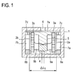
- Fig. 1 shows a structure described in Patent literature 1 as a conventional example of this type of microphone.
- two electret condenser microphone units are disposed in a holder 1.
- the microphone units have diaphragms 2a and 2b, and opposite electrodes (back plates) 3a and 3b are respectively disposed opposite to the diaphragms 2a and 2b.
- the opposite electrodes 3a and 3b are connected to the gate terminal of a field effect transistor (FET) 4.
- FET field effect transistor
- the opposite electrodes 3a and 3b and the FET 4 are supported by a supporting member 5, and the opposite electrodes 3a and 3b are disposed opposite each other with the FET 4 placed therebetween.
- the diaphragms 2a and 2b are positioned at the outer sides of the opposite electrodes 3a and 3b, respectively.
- the holder 1 has a through hole 6 and also has a narrow gap 7e between the supporting member 5 and the inner wall of the holder 1.
- Ringshaped members 8a and 8b provided at the outer sides of the diaphragms 2a and 2b in order to form outer cavities 7a and 7b are cut to form paths 7c and 7d, respectively.
- in-phase output signals can be obtained from the two microphone units for the input sound waves, whereas opposite-phase outputs can be obtained for vibration noise caused by mechanical vibration, allowing the vibration noise to be canceled.
- the two diaphragms 2a and 2b are disposed at both ends of the microphone; in other words, the two diaphragms 2a and 2b are disposed far apart. Therefore, when the vibration source is located beside a side wall (the left or right) of the holder 1, for example, the difference ⁇ L 1 in distance from the vibration source to the two diaphragms 2a and 2b is large, which is a disadvantage in canceling the vibration noise caused by the mechanical vibration.
- an object of the present invention is to provide a microphone having a high vibration-noise canceling effect by making the distance between two diaphragms very small.
- a microphone capable of canceling vibration noise caused by mechanical vibration includes a pair of diaphragms and a pair of back plates opposite the respective diaphragms in a capsule; a printed circuit board is disposed at the middle of the capsule; and the pair of diaphragms are disposed close and opposite to the surfaces of the printed circuit board, respectively, with the printed circuit board disposed therebetween.
- the distance between the two diaphragms is made very small, which makes the difference in distance from the vibration source to the two diaphragms small. Therefore, a high canceling effect is obtained with respect to vibration noise caused by mechanical vibration.
- Figs. 2A and 2B show the appearance of a microphone according to an embodiment of the present invention.
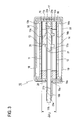
- Fig. 3 shows the cross sectional structure thereof.
- Fig. 4 shows an exploded view thereof.
- a microphone 10 is formed of a pair of diaphragms 11 and 12 glued to and supported by rings 11a and 12a, a pair of back plates 13 and 14, a pair of spacers 15 and 16, a printed circuit board 17 on which predetermined patterns are formed and components are mounted, and a capsule for accommodating the above.
- the capsule is divided into two upper and lower capsules 18 and 19, and these capsules 18 and 19 are cylinders with one end face closed, as shown in Fig. 4 .
- the capsule 18 is cut from an open end face at a cylindrical wall to form an opening 18a.
- the capsule 19 is cut from an open end face at a cylindrical wall to form an opening 19a.
- a protruding piece 19b is bent from the capsule 19 at an inner end (close to the closed end face) of the opening 19a so as to protrude toward the outside.
- the capsule 18 is slightly smaller in diameter than the capsule 19, so that the capsule 18 can be put inside the capsule 19.
- Fig. 4 shows a state in which the open end face of the capsule 19 is crimped in assembly, which will be described later.
- the pair of back plates 13 and 14 are circular and have four through holes 13a and 14a on their plate faces, respectively.
- the back plates 13 and 14 have peripheral walls 13b and 14b having a predetermined height at their circumferences, respectively.
- the back plates 13 and 14 having the peripheral walls 13b and 14b can be formed, for example, by drawing. Electrets are formed on the faces of the back plates 13 and 14, which oppose the diaphragms 11 and 12, but they are not shown in the drawings.
- the spacers 15 and 16 are made from an insulating material and are ring shaped in the same way as the rings 11a and 12a, which support the diaphragms 11 and 12.
- the printed circuit board 17 is formed of a circular part 17a and a rectangular protruding part 17b protruding from a part of the circumference of the circular part 17a.
- Figs. 5A and 5B show details of the printed circuit board 17.
- the printed circuit board 17 has a large opening 21 from the protruding part 17b to the center of the circular part 17a.
- the opening 21 has a semi-circular part 21a concentric with the circular part 17a in the circular part 17a, and an extending part 21b extending from the semi-circular part 21a to the protruding part 17b.
- an arc-shaped pattern 22a concentric with the circular part 17a and three island-shaped patterns 22b, 22c, and 22d are formed on the upper surface of the circular part 17a of the printed circuit board 17.
- a pattern 22e is formed at the center of the circumference of the arc-shaped pattern 22a in a protruding manner toward the center of the circular part 17a.
- Terminals 22f and 22g connected to the patterns 22b and 22d, respectively, are formed on the upper surface of the protruding part 17b.
- an arc-shaped pattern 23a and three island-shaped patterns 23b, 23c, and 23d are formed on the lower surface of the circular part 17a in the same manner as on the upper surface.
- a pattern 23e connected to the pattern 23d is formed on the lower surface of the protruding part 17b.
- the patterns 22a and 23a, the patterns 22b and 23b, the patterns 22c and 23c, the patterns 22d and 23d, and the terminal 22g and the pattern 23e are electrically connected to each other via through holes 24.
- hatched portions with broken lines indicate areas coated with resist 25.
- Figs. 6A and 6B show the printed circuit board 17 structured in the foregoing manner with components mounted thereon.
- An FET 26 is mounted on the upper surface of the printed circuit board 17, as shown in Fig. 6A
- a capacitor 27 and a resistor 28 are mounted on the lower surface of the printed circuit board 17, as shown in Fig. 6B .
- the back plate 13, the spacer 15, the ring 11a supporting the diaphragm 11, the printed circuit board 17 with the components mounted thereon, the ring 12a supporting the diaphragm 12, the spacer 16, and the back plate 14 are sequentially put into the capsule 18 in stacked manner, then the capsule 18 is covered with the capsule 19, and the open end of the capsule 19 is crimped to assemble the microphone 10.
- the openings 18a and 19a of the capsules 18 and 19 are positioned at the same location, and the protruding part 17b of the printed circuit board 17 protrudes toward the outside of the capsules 18 and 19 from an opening 29 formed when the openings 18a and 19a are positioned.
- the protruding piece 19b of the capsule 19 is disposed so as to face and contact the lower surface of the protruding part 17b of the printed circuit board 17, and the protruding piece 19b is connected to the pattern 23e formed on the protruding part 17b by soldering to complete the microphone 10, as shown in Figs. 2A, 2B , and 3 .
- a two-dot chain line shows an area where solder 31 is applied.
- the pair of diaphragms 11 and 12 face the back plates 13 and 14 with the spacers 15 and 16 placed therebetween, respectively, and the pair of diaphragms 11 and 12 are disposed so as to be close and opposite to the surfaces of the printed circuit board 17 with the printed circuit board 17 placed therebetween.
- the rings 11a and 12a respectively supporting the diaphragms 11 and 12 face and contact the patterns 22a and 23a of the printed circuit board 17, respectively, so that the pair of diaphragms 11 and 12 are connected to the gate terminal of the FET 26.
- the extending part 21b of the opening 21 of the printed circuit board 17 is partially exposed to the outside.
- sound waves are input to the capsules 18 and 19 through the opening 21 of the printed circuit board 17 and are transmitted to the diaphragms 11 and 12.
- the back plates 13 and 14 serve as back chambers that support the stiffness of the diaphragms 11 and 12.
- the peripheral walls 13b and 14b are provided for the back plates 13 and 14, respectively, by drawing, and spaces surrounded by the peripheral walls 13b and 14b are covered with the closed end faces of the capsules 18 and 19 to form back chambers 32 and 33.
- the back chambers 32 and 33 can be easily formed without using any other members.
- the pair of diaphragms 11 and 12 are provided to allow in-phase output signals to be generated for input sound waves and opposite-phase outputs to be generated for vibration noise caused by mechanical vibration, so that the vibration noise can be canceled. Since the pair of diaphragms 11 and 12 are disposed so as to be close to and face each other with the printed circuit board 17 placed therebetween, the difference ⁇ L 2 in distance from the vibration source to the two diaphragms 11 and 12 is made much smaller in this embodiment compared with that for the conventional microphone shown in Fig. 1 . Therefore, the microphone 10 has a higher vibration-noise canceling effect than the conventional microphone.
- the sound waves can be guided to the upper and lower vibration systems (the pair of diaphragms 11 and 12) uniformly.
- the rings 11a and 12a respectively supporting the diaphragms 11 and 12 directly face and contact the patterns 22a and 23a of the printed circuit board 17, respectively, in other words, since the rings 11a and 12a for the diaphragms 11 and 12 also serve as the gate ring of the FET 26, the structure is made simpler, the stray capacitance around the gate of the FET 26 is reduced, and a high output is possible.
- the terminals 22f and 22g formed on the protruding part 17b of the printed circuit board 17 are connected to terminals on a printed circuit board of the electronic device with lead wires.
- the microphone 10 is placed in a rubber holder before being mounted.
- Figs. 7A, 7B, and 7C show the microphone 10 to which a holder 41 is attached.
- the holder 41 has a protruding part 41a corresponding to the protruding part 17b of the printed circuit board 17.
- the protruding part 41a has an opening 41b connected to the opening 21 of the printed circuit board 17.
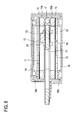
- Fig. 8 shows a microphone according to another embodiment of the present invention.
- the closed end faces of the capsules 18 and 19 are made to have gutters, as shown in Fig. 8 ; in other words, projections 18b and 19c protruding inward are formed in the circumference at peripheral portions of the closed end faces of the capsules 18 and 19, respectively, to make back chambers 32 and 33.
- the back plates 13 and 14 are simple circular plates. Spaces surrounded by the projections 18b and 19c are covered with the back plates 13 and 14 to form the back chambers 32 and 33. Such a structure can be employed.
- sound waves are input to the microphone from the opening 21 of the printed circuit board 17; in other words, sound waves are input from a side of the microphone.
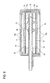
- another structure may be used in which sound holes 18c and 19d are formed in the closed end faces of the capsules 18 and 19, as shown in Fig. 9 , so that sound waves are input from the upper and lower directions of the microphone.
- the printed circuit board 17 does not have the opening 21, and the back chambers 32 and 33 are formed between the printed circuit board 17 and the diaphragms 11 and 12.
- a microphone according to the present invention is effective when used as a vibration canceling microphone for canceling zooming sounds in a digital video camera (DVC) or a digital still camera (DSC), and can be applied, for example, to a device that requires countermeasures for vibration such as noise caused by touch.
- DVC digital video camera
- DSC digital still camera
Landscapes
- Physics & Mathematics (AREA)
- Engineering & Computer Science (AREA)
- Acoustics & Sound (AREA)
- Signal Processing (AREA)
- Health & Medical Sciences (AREA)
- Otolaryngology (AREA)
- Electrostatic, Electromagnetic, Magneto- Strictive, And Variable-Resistance Transducers (AREA)
- Details Of Audible-Bandwidth Transducers (AREA)
- Obtaining Desirable Characteristics In Audible-Bandwidth Transducers (AREA)
Abstract
Description
- The present invention relates to a microphone structured to be capable of canceling vibration noise caused by mechanical vibration.
-
Fig. 1 shows a structure described in Patent literature 1 as a conventional example of this type of microphone. - In this example, two electret condenser microphone units are disposed in a holder 1. In
Fig. 1 , the microphone units havediaphragms diaphragms opposite electrodes - The
opposite electrodes FET 4 are supported by a supportingmember 5, and theopposite electrodes FET 4 placed therebetween. Thediaphragms opposite electrodes - The holder 1 has a through
hole 6 and also has anarrow gap 7e between the supportingmember 5 and the inner wall of the holder 1. Ringshapedmembers diaphragms outer cavities paths - Sound waves input from the through
hole 6 pass through thenarrow gap 7e, thepaths outer cavities diaphragms inner cavities opposite electrodes - With this structure, in-phase output signals can be obtained from the two microphone units for the input sound waves, whereas opposite-phase outputs can be obtained for vibration noise caused by mechanical vibration, allowing the vibration noise to be canceled.
-
- [Patent literature 1] Japanese Patent Application Laid-Open No.
02-41099 2748417 - In the microphone structured as described above, the two
diaphragms diaphragms diaphragms - Accordingly, an object of the present invention is to provide a microphone having a high vibration-noise canceling effect by making the distance between two diaphragms very small.
- According to the present invention, a microphone capable of canceling vibration noise caused by mechanical vibration includes a pair of diaphragms and a pair of back plates opposite the respective diaphragms in a capsule; a printed circuit board is disposed at the middle of the capsule; and the pair of diaphragms are disposed close and opposite to the surfaces of the printed circuit board, respectively, with the printed circuit board disposed therebetween.
- According to the present invention, the distance between the two diaphragms is made very small, which makes the difference in distance from the vibration source to the two diaphragms small. Therefore, a high canceling effect is obtained with respect to vibration noise caused by mechanical vibration.
-
-
Fig. 1 is a cross sectional view showing the structure of a conventional microphone; -
Fig. 2A is a perspective view of the appearance of a microphone according to an embodiment of the present invention, seen from an upper side, andFig. 2B is a perspective view of the microphone shown inFig. 2A , seen from a lower side; -
Fig. 3 is a cross sectional view of the microphone shown inFigs. 2A and 2B ; -
Fig. 4 is an exploded perspective view of the microphone shown inFigs. 2A and 2B ; -
Fig. 5A is a view showing pattern details on a printed circuit board, seen from an upper side, andFig. 5B is a view showing pattern details on the printed circuit board, seen from a lower side; -
Fig. 6A is a perspective view showing the printed circuit board with a component mounted thereon, seen from an upper side, andFig. 6B is a perspective view showing the printed circuit board with components mounted thereon, seen from a lower side; -
Fig. 7A is a perspective view of the microphone shown inFigs. 2A and 2B with a holder mounted thereon, seen from an upper side,Fig. 7B is a perspective view of the microphone shown inFigs. 2A and 2B with the holder mounted thereon, seen from a lower side, andFig. 7C is a cross sectional view of the microphone shown inFigs. 2A and 2B with the holder mounted thereon; -
Fig. 8 is a cross sectional view of a microphone according to another embodiment of the present invention; and -
Fig. 9 is a cross sectional view of a microphone according to a modification of the present invention. - Embodiments of the present invention will be described below.
-
Figs. 2A and 2B show the appearance of a microphone according to an embodiment of the present invention.Fig. 3 shows the cross sectional structure thereof.Fig. 4 shows an exploded view thereof. In this embodiment, amicrophone 10 is formed of a pair ofdiaphragms rings back plates spacers circuit board 17 on which predetermined patterns are formed and components are mounted, and a capsule for accommodating the above. - In this embodiment, the capsule is divided into two upper and
lower capsules capsules Fig. 4 . - The
capsule 18 is cut from an open end face at a cylindrical wall to form an opening 18a. In the same way, thecapsule 19 is cut from an open end face at a cylindrical wall to form an opening 19a. Aprotruding piece 19b is bent from thecapsule 19 at an inner end (close to the closed end face) of the opening 19a so as to protrude toward the outside. - The
capsule 18 is slightly smaller in diameter than thecapsule 19, so that thecapsule 18 can be put inside thecapsule 19.Fig. 4 shows a state in which the open end face of thecapsule 19 is crimped in assembly, which will be described later. - The pair of
back plates holes back plates peripheral walls back plates peripheral walls back plates diaphragms - The
spacers rings diaphragms - The printed
circuit board 17 is formed of acircular part 17a and a rectangular protrudingpart 17b protruding from a part of the circumference of thecircular part 17a.Figs. 5A and 5B show details of the printedcircuit board 17. The printedcircuit board 17 has alarge opening 21 from the protrudingpart 17b to the center of thecircular part 17a. Theopening 21 has asemi-circular part 21a concentric with thecircular part 17a in thecircular part 17a, and an extendingpart 21b extending from thesemi-circular part 21a to theprotruding part 17b. - As shown in
Fig. 5A , an arc-shapedpattern 22a concentric with thecircular part 17a and three island-shapedpatterns circular part 17a of the printedcircuit board 17. Apattern 22e is formed at the center of the circumference of the arc-shapedpattern 22a in a protruding manner toward the center of thecircular part 17a.Terminals patterns protruding part 17b. - As shown in
Fig. 5B , an arc-shapedpattern 23a and three island-shapedpatterns circular part 17a in the same manner as on the upper surface. Apattern 23e connected to thepattern 23d is formed on the lower surface of theprotruding part 17b. Thepatterns patterns patterns patterns pattern 23e are electrically connected to each other via throughholes 24. InFigs. 5A and 5B , hatched portions with broken lines indicate areas coated with resist 25. -
Figs. 6A and 6B show the printedcircuit board 17 structured in the foregoing manner with components mounted thereon. AnFET 26 is mounted on the upper surface of the printedcircuit board 17, as shown inFig. 6A , and acapacitor 27 and aresistor 28 are mounted on the lower surface of the printedcircuit board 17, as shown inFig. 6B . - The assembly of the
microphone 10 will be described next. - The
back plate 13, thespacer 15, thering 11a supporting thediaphragm 11, the printedcircuit board 17 with the components mounted thereon, thering 12a supporting thediaphragm 12, thespacer 16, and theback plate 14 are sequentially put into thecapsule 18 in stacked manner, then thecapsule 18 is covered with thecapsule 19, and the open end of thecapsule 19 is crimped to assemble themicrophone 10. - When assembling the
microphone 10, theopenings capsules protruding part 17b of the printedcircuit board 17 protrudes toward the outside of thecapsules opening 29 formed when theopenings piece 19b of thecapsule 19 is disposed so as to face and contact the lower surface of theprotruding part 17b of the printedcircuit board 17, and the protrudingpiece 19b is connected to thepattern 23e formed on theprotruding part 17b by soldering to complete themicrophone 10, as shown inFigs. 2A, 2B , and3 . InFig. 2B , a two-dot chain line shows an area wheresolder 31 is applied. - The pair of
diaphragms back plates spacers diaphragms circuit board 17 with the printedcircuit board 17 placed therebetween. - The
rings diaphragms patterns circuit board 17, respectively, so that the pair ofdiaphragms FET 26. - The extending
part 21b of theopening 21 of the printedcircuit board 17 is partially exposed to the outside. In this embodiment, sound waves are input to thecapsules opening 21 of the printedcircuit board 17 and are transmitted to thediaphragms - Since the
diaphragms circuit board 17 and the printedcircuit board 17 serves as a sound inlet in the way described above, theback plates diaphragms peripheral walls back plates peripheral walls capsules chambers back chambers - According to the
microphone 10 structured as described above, the pair ofdiaphragms diaphragms circuit board 17 placed therebetween, the difference ΔL2 in distance from the vibration source to the twodiaphragms Fig. 1 . Therefore, themicrophone 10 has a higher vibration-noise canceling effect than the conventional microphone. - In this embodiment, since sound waves are input to the
microphone 10 from theopening 21 of the printedcircuit board 17, the sound waves can be guided to the upper and lower vibration systems (the pair ofdiaphragms 11 and 12) uniformly. In addition, in this embodiment, since therings diaphragms patterns circuit board 17, respectively, in other words, since therings diaphragms FET 26, the structure is made simpler, the stray capacitance around the gate of theFET 26 is reduced, and a high output is possible. - When the
microphone 10 is mounted in an electronic device, theterminals protruding part 17b of the printedcircuit board 17 are connected to terminals on a printed circuit board of the electronic device with lead wires. Usually, themicrophone 10 is placed in a rubber holder before being mounted.Figs. 7A, 7B, and 7C show themicrophone 10 to which aholder 41 is attached. - The
holder 41 has aprotruding part 41a corresponding to theprotruding part 17b of the printedcircuit board 17. Theprotruding part 41a has anopening 41b connected to theopening 21 of the printedcircuit board 17. -
Fig. 8 shows a microphone according to another embodiment of the present invention. Unlike in the foregoing embodiment, in which theback plates peripheral walls back chambers capsules Fig. 8 ; in other words,projections capsules chambers back plates projections back plates back chambers - In the above-described embodiments, sound waves are input to the microphone from the
opening 21 of the printedcircuit board 17; in other words, sound waves are input from a side of the microphone. Instead of that structure, another structure may be used in which soundholes capsules Fig. 9 , so that sound waves are input from the upper and lower directions of the microphone. In that case, the printedcircuit board 17 does not have theopening 21, and theback chambers circuit board 17 and thediaphragms - A microphone according to the present invention is effective when used as a vibration canceling microphone for canceling zooming sounds in a digital video camera (DVC) or a digital still camera (DSC), and can be applied, for example, to a device that requires countermeasures for vibration such as noise caused by touch.
Claims (8)
- A microphone capable of canceling vibration noise caused by mechanical vibration, comprising in a capsule:a pair of diaphragms; anda pair of back plates opposite to the respective diaphragms;a printed circuit board being disposed at the middle of the capsule; andthe pair of diaphragms being disposed close and opposite to the surfaces of the printed circuit board, respectively, with the printed circuit board disposed therebetween.
- The microphone according to Claim 1,
wherein the printed circuit board has a protruding part protruding toward the outside of the capsule, and the printed circuit board has an opening a part of which is located at the protruding part; and
sound waves are input to the capsule through the opening. - The microphone according to Claim 2,
wherein the printed circuit board has a circular part accommodated in the capsule and the protruding part, which protrudes from a part of the circumference of the circular part, and
the opening extends to the center of the circular part. - The microphone according to Claim 2,
wherein the protruding part protrudes toward the outside of the capsule from an opening of the capsule, and
a protruding piece is formed at the opening of the capsule to face and contact the protruding part. - The microphone according to Claim 2, wherein an external-connection terminal is formed at the protruding part.
- The microphone according to one of Claims 1 to 5,
wherein the pair of diaphragms are respectively glued to and supported by rings; and
the rings face and contact the printed circuit board. - The microphone according to one of Claims 1 to 5, wherein the back plates have peripheral walls and spaces surrounded by the peripheral walls are covered by end faces of the capsule to form back chambers.
- The microphone according to one of Claims 1 to 5, wherein projections protruding inward are formed in a circumference at peripheral portions of end faces of the capsule, and spaces surrounded by the protruding projections are covered by the back plates to form back chambers.
Applications Claiming Priority (2)
| Application Number | Priority Date | Filing Date | Title |
|---|---|---|---|
| JP2010087479A JP5613434B2 (en) | 2010-04-06 | 2010-04-06 | Microphone |
| PCT/JP2011/055644 WO2011125409A1 (en) | 2010-04-06 | 2011-03-10 | Microphone |
Publications (3)
| Publication Number | Publication Date |
|---|---|
| EP2557812A1 true EP2557812A1 (en) | 2013-02-13 |
| EP2557812A4 EP2557812A4 (en) | 2013-11-20 |
| EP2557812B1 EP2557812B1 (en) | 2017-06-07 |
Family
ID=44762370
Family Applications (1)
| Application Number | Title | Priority Date | Filing Date |
|---|---|---|---|
| EP11765311.3A Active EP2557812B1 (en) | 2010-04-06 | 2011-03-10 | Microphone |
Country Status (7)
| Country | Link |
|---|---|
| US (1) | US8879752B2 (en) |
| EP (1) | EP2557812B1 (en) |
| JP (1) | JP5613434B2 (en) |
| KR (1) | KR101305983B1 (en) |
| CN (1) | CN102812726B (en) |
| TW (1) | TWI504280B (en) |
| WO (1) | WO2011125409A1 (en) |
Families Citing this family (16)
| Publication number | Priority date | Publication date | Assignee | Title |
|---|---|---|---|---|
| JP5626907B2 (en) * | 2011-09-13 | 2014-11-19 | ホシデン株式会社 | Electret condenser type sounding body |
| WO2014024671A1 (en) * | 2012-08-06 | 2014-02-13 | ダイキン工業株式会社 | Resin composition and molded article |
| DE102013214823A1 (en) * | 2013-07-30 | 2015-02-05 | Robert Bosch Gmbh | Microphone component with at least two MEMS microphone components |
| TWI558224B (en) * | 2013-09-13 | 2016-11-11 | 宏碁股份有限公司 | Microphone module and electronic device |
| CN104796830B (en) * | 2014-01-22 | 2018-05-11 | 宏碁股份有限公司 | Microphone module and electronic device |
| US9510107B2 (en) * | 2014-03-06 | 2016-11-29 | Infineon Technologies Ag | Double diaphragm MEMS microphone without a backplate element |
| TWI548285B (en) * | 2015-03-13 | 2016-09-01 | Taiwan Carol Electronics Co Ltd | Active anti - vibration microphone |
| CN107849376B (en) * | 2015-07-17 | 2021-11-30 | 日产化学工业株式会社 | Non-aqueous ink composition comprising metal nanoparticles suitable for organic electronics |
| US11179886B2 (en) | 2016-01-21 | 2021-11-23 | 3M Innovative Properties Company | Additive processing of fluoropolymers |
| US10412503B2 (en) | 2016-08-12 | 2019-09-10 | Shure Acquisition Holdings, Inc. | Microphone and methods of assembling microphones |
| JP6945390B2 (en) * | 2017-08-25 | 2021-10-06 | ホシデン株式会社 | Mike Assembly |
| JP7405074B2 (en) | 2018-04-13 | 2023-12-26 | Agc株式会社 | Speaker diaphragm and medical catheter |
| CN108989959B (en) * | 2018-08-09 | 2020-11-10 | 京东方科技集团股份有限公司 | Electret microphone, manufacturing method thereof and display device |
| US11558695B2 (en) | 2020-03-31 | 2023-01-17 | Shure Acquisition Holdings, Inc. | Condenser microphone pattern adjustment |
| JP7351792B2 (en) | 2020-04-30 | 2023-09-27 | ホシデン株式会社 | sound collection device |
| US20230010149A1 (en) * | 2021-07-07 | 2023-01-12 | Private MONK Inc. | Voice isolation device |
Family Cites Families (19)
| Publication number | Priority date | Publication date | Assignee | Title |
|---|---|---|---|---|
| JP2748417B2 (en) * | 1988-07-30 | 1998-05-06 | ソニー株式会社 | Microphone device |
| JP3141745B2 (en) * | 1995-07-25 | 2001-03-05 | 松下電器産業株式会社 | Acceleration sensor |
| KR100336296B1 (en) * | 1999-07-30 | 2002-05-13 | 장세열 | Electric-Acoustic Transducer Having Dual Voice Coil Drivers |
| US7130434B1 (en) * | 2003-03-26 | 2006-10-31 | Plantronics, Inc. | Microphone PCB with integrated filter |
| JP3103711U (en) * | 2003-10-24 | 2004-08-19 | 台湾楼氏電子工業股▼ふん▲有限公司 | High efficiency condenser microphone |
| US7224812B2 (en) * | 2004-01-13 | 2007-05-29 | Taiwan Carol Electronics Co., Ltd. | Condenser microphone and method for making the same |
| JP2005354581A (en) * | 2004-06-14 | 2005-12-22 | Nikon Corp | Electronics and camera |
| JP2006140740A (en) * | 2004-11-11 | 2006-06-01 | Toshiba Corp | Audio generator |
| JP4615972B2 (en) * | 2004-11-29 | 2011-01-19 | 株式会社オーディオテクニカ | Condenser microphone unit |
| JP4403412B2 (en) * | 2005-04-22 | 2010-01-27 | ソニー株式会社 | Microphone |
| JP2007174165A (en) * | 2005-12-21 | 2007-07-05 | Rion Co Ltd | Microphone and hearing aid using the same |
| US8509459B1 (en) * | 2005-12-23 | 2013-08-13 | Plantronics, Inc. | Noise cancelling microphone with reduced acoustic leakage |
| JP2007306216A (en) * | 2006-05-10 | 2007-11-22 | Hosiden Corp | Electret capacitor microphone |
| US7729500B2 (en) * | 2006-12-19 | 2010-06-01 | Fortmedia, Inc. | Microphone array with electromagnetic interference shielding means |
| JP2008199227A (en) * | 2007-02-09 | 2008-08-28 | Yamaha Corp | Condenser microphone device |
| US20080192962A1 (en) * | 2007-02-13 | 2008-08-14 | Sonion Nederland B.V. | Microphone with dual transducers |
| US8705775B2 (en) * | 2007-04-25 | 2014-04-22 | University Of Florida Research Foundation, Inc. | Capacitive microphone with integrated cavity |
| EP2007167A3 (en) * | 2007-06-21 | 2013-01-23 | Funai Electric Advanced Applied Technology Research Institute Inc. | Voice input-output device and communication device |
| TW200942067A (en) * | 2008-03-26 | 2009-10-01 | Univ Nat Chunghsing | Voice-electric conversion chip of ribbon microphone |
-
2010
- 2010-04-06 JP JP2010087479A patent/JP5613434B2/en active Active
-
2011
- 2011-03-09 TW TW100107917A patent/TWI504280B/en active
- 2011-03-10 KR KR1020127022351A patent/KR101305983B1/en active Active
- 2011-03-10 EP EP11765311.3A patent/EP2557812B1/en active Active
- 2011-03-10 WO PCT/JP2011/055644 patent/WO2011125409A1/en not_active Ceased
- 2011-03-10 CN CN201180015721.4A patent/CN102812726B/en active Active
- 2011-03-10 US US13/583,474 patent/US8879752B2/en not_active Expired - Fee Related
Also Published As
| Publication number | Publication date |
|---|---|
| US20130010981A1 (en) | 2013-01-10 |
| TWI504280B (en) | 2015-10-11 |
| JP2011223133A (en) | 2011-11-04 |
| US8879752B2 (en) | 2014-11-04 |
| KR101305983B1 (en) | 2013-09-12 |
| CN102812726B (en) | 2015-03-25 |
| EP2557812A4 (en) | 2013-11-20 |
| EP2557812B1 (en) | 2017-06-07 |
| TW201143473A (en) | 2011-12-01 |
| KR20120127622A (en) | 2012-11-22 |
| JP5613434B2 (en) | 2014-10-22 |
| WO2011125409A1 (en) | 2011-10-13 |
| CN102812726A (en) | 2012-12-05 |
Similar Documents
| Publication | Publication Date | Title |
|---|---|---|
| US8879752B2 (en) | Microphone | |
| TWI376963B (en) | ||
| JP4751057B2 (en) | Condenser microphone and manufacturing method thereof | |
| EP2190215A1 (en) | Condenser microphone | |
| EP1748676B1 (en) | Electro-acoustic transducer | |
| US20080310657A1 (en) | Electret condenser microphone | |
| KR102339558B1 (en) | Microphone unit | |
| US8150078B2 (en) | Electret condenser microphone | |
| JP2010166286A (en) | Structure for mounting silicon microphone, and electronic apparatus | |
| KR200449885Y1 (en) | Spacer Integrated Diaphragm for Condenser Microphone | |
| JP2006238203A (en) | Microphone | |
| JP2008219435A (en) | Capacitor microphone | |
| JP5626907B2 (en) | Electret condenser type sounding body | |
| JP2008035045A (en) | Condenser microphone | |
| JP2008098851A (en) | Capacitor microphone | |
| JP2013187788A (en) | Non-directional microphone |
Legal Events
| Date | Code | Title | Description |
|---|---|---|---|
| PUAI | Public reference made under article 153(3) epc to a published international application that has entered the european phase |
Free format text: ORIGINAL CODE: 0009012 |
|
| 17P | Request for examination filed |
Effective date: 20121106 |
|
| AK | Designated contracting states |
Kind code of ref document: A1 Designated state(s): AL AT BE BG CH CY CZ DE DK EE ES FI FR GB GR HR HU IE IS IT LI LT LU LV MC MK MT NL NO PL PT RO RS SE SI SK SM TR |
|
| DAX | Request for extension of the european patent (deleted) | ||
| A4 | Supplementary search report drawn up and despatched |
Effective date: 20131022 |
|
| RIC1 | Information provided on ipc code assigned before grant |
Ipc: H04R 1/38 20060101AFI20131016BHEP Ipc: H04R 1/02 20060101ALI20131016BHEP Ipc: H04R 19/01 20060101ALI20131016BHEP |
|
| GRAP | Despatch of communication of intention to grant a patent |
Free format text: ORIGINAL CODE: EPIDOSNIGR1 |
|
| STAA | Information on the status of an ep patent application or granted ep patent |
Free format text: STATUS: GRANT OF PATENT IS INTENDED |
|
| INTG | Intention to grant announced |
Effective date: 20170102 |
|
| GRAS | Grant fee paid |
Free format text: ORIGINAL CODE: EPIDOSNIGR3 |
|
| GRAA | (expected) grant |
Free format text: ORIGINAL CODE: 0009210 |
|
| STAA | Information on the status of an ep patent application or granted ep patent |
Free format text: STATUS: THE PATENT HAS BEEN GRANTED |
|
| AK | Designated contracting states |
Kind code of ref document: B1 Designated state(s): AL AT BE BG CH CY CZ DE DK EE ES FI FR GB GR HR HU IE IS IT LI LT LU LV MC MK MT NL NO PL PT RO RS SE SI SK SM TR |
|
| REG | Reference to a national code |
Ref country code: GB Ref legal event code: FG4D |
|
| GRAA | (expected) grant |
Free format text: ORIGINAL CODE: 0009210 |
|
| REG | Reference to a national code |
Ref country code: CH Ref legal event code: EP Ref country code: AT Ref legal event code: REF Ref document number: 900011 Country of ref document: AT Kind code of ref document: T Effective date: 20170615 |
|
| REG | Reference to a national code |
Ref country code: IE Ref legal event code: FG4D |
|
| REG | Reference to a national code |
Ref country code: DE Ref legal event code: R096 Ref document number: 602011038541 Country of ref document: DE |
|
| REG | Reference to a national code |
Ref country code: SE Ref legal event code: TRGR |
|
| REG | Reference to a national code |
Ref country code: NL Ref legal event code: MP Effective date: 20170607 |
|
| REG | Reference to a national code |
Ref country code: LT Ref legal event code: MG4D |
|
| PG25 | Lapsed in a contracting state [announced via postgrant information from national office to epo] |
Ref country code: HR Free format text: LAPSE BECAUSE OF FAILURE TO SUBMIT A TRANSLATION OF THE DESCRIPTION OR TO PAY THE FEE WITHIN THE PRESCRIBED TIME-LIMIT Effective date: 20170607 Ref country code: ES Free format text: LAPSE BECAUSE OF FAILURE TO SUBMIT A TRANSLATION OF THE DESCRIPTION OR TO PAY THE FEE WITHIN THE PRESCRIBED TIME-LIMIT Effective date: 20170607 Ref country code: NO Free format text: LAPSE BECAUSE OF FAILURE TO SUBMIT A TRANSLATION OF THE DESCRIPTION OR TO PAY THE FEE WITHIN THE PRESCRIBED TIME-LIMIT Effective date: 20170907 Ref country code: GR Free format text: LAPSE BECAUSE OF FAILURE TO SUBMIT A TRANSLATION OF THE DESCRIPTION OR TO PAY THE FEE WITHIN THE PRESCRIBED TIME-LIMIT Effective date: 20170908 Ref country code: LT Free format text: LAPSE BECAUSE OF FAILURE TO SUBMIT A TRANSLATION OF THE DESCRIPTION OR TO PAY THE FEE WITHIN THE PRESCRIBED TIME-LIMIT Effective date: 20170607 |
|
| REG | Reference to a national code |
Ref country code: AT Ref legal event code: MK05 Ref document number: 900011 Country of ref document: AT Kind code of ref document: T Effective date: 20170607 |
|
| PG25 | Lapsed in a contracting state [announced via postgrant information from national office to epo] |
Ref country code: BG Free format text: LAPSE BECAUSE OF FAILURE TO SUBMIT A TRANSLATION OF THE DESCRIPTION OR TO PAY THE FEE WITHIN THE PRESCRIBED TIME-LIMIT Effective date: 20170907 Ref country code: LV Free format text: LAPSE BECAUSE OF FAILURE TO SUBMIT A TRANSLATION OF THE DESCRIPTION OR TO PAY THE FEE WITHIN THE PRESCRIBED TIME-LIMIT Effective date: 20170607 Ref country code: NL Free format text: LAPSE BECAUSE OF FAILURE TO SUBMIT A TRANSLATION OF THE DESCRIPTION OR TO PAY THE FEE WITHIN THE PRESCRIBED TIME-LIMIT Effective date: 20170607 Ref country code: RS Free format text: LAPSE BECAUSE OF FAILURE TO SUBMIT A TRANSLATION OF THE DESCRIPTION OR TO PAY THE FEE WITHIN THE PRESCRIBED TIME-LIMIT Effective date: 20170607 |
|
| PG25 | Lapsed in a contracting state [announced via postgrant information from national office to epo] |
Ref country code: CZ Free format text: LAPSE BECAUSE OF FAILURE TO SUBMIT A TRANSLATION OF THE DESCRIPTION OR TO PAY THE FEE WITHIN THE PRESCRIBED TIME-LIMIT Effective date: 20170607 Ref country code: RO Free format text: LAPSE BECAUSE OF FAILURE TO SUBMIT A TRANSLATION OF THE DESCRIPTION OR TO PAY THE FEE WITHIN THE PRESCRIBED TIME-LIMIT Effective date: 20170607 Ref country code: SK Free format text: LAPSE BECAUSE OF FAILURE TO SUBMIT A TRANSLATION OF THE DESCRIPTION OR TO PAY THE FEE WITHIN THE PRESCRIBED TIME-LIMIT Effective date: 20170607 Ref country code: AT Free format text: LAPSE BECAUSE OF FAILURE TO SUBMIT A TRANSLATION OF THE DESCRIPTION OR TO PAY THE FEE WITHIN THE PRESCRIBED TIME-LIMIT Effective date: 20170607 Ref country code: EE Free format text: LAPSE BECAUSE OF FAILURE TO SUBMIT A TRANSLATION OF THE DESCRIPTION OR TO PAY THE FEE WITHIN THE PRESCRIBED TIME-LIMIT Effective date: 20170607 |
|
| REG | Reference to a national code |
Ref country code: FR Ref legal event code: PLFP Year of fee payment: 8 |
|
| PG25 | Lapsed in a contracting state [announced via postgrant information from national office to epo] |
Ref country code: PL Free format text: LAPSE BECAUSE OF FAILURE TO SUBMIT A TRANSLATION OF THE DESCRIPTION OR TO PAY THE FEE WITHIN THE PRESCRIBED TIME-LIMIT Effective date: 20170607 Ref country code: SM Free format text: LAPSE BECAUSE OF FAILURE TO SUBMIT A TRANSLATION OF THE DESCRIPTION OR TO PAY THE FEE WITHIN THE PRESCRIBED TIME-LIMIT Effective date: 20170607 Ref country code: IS Free format text: LAPSE BECAUSE OF FAILURE TO SUBMIT A TRANSLATION OF THE DESCRIPTION OR TO PAY THE FEE WITHIN THE PRESCRIBED TIME-LIMIT Effective date: 20171007 Ref country code: IT Free format text: LAPSE BECAUSE OF FAILURE TO SUBMIT A TRANSLATION OF THE DESCRIPTION OR TO PAY THE FEE WITHIN THE PRESCRIBED TIME-LIMIT Effective date: 20170607 |
|
| REG | Reference to a national code |
Ref country code: DE Ref legal event code: R097 Ref document number: 602011038541 Country of ref document: DE |
|
| PLBE | No opposition filed within time limit |
Free format text: ORIGINAL CODE: 0009261 |
|
| STAA | Information on the status of an ep patent application or granted ep patent |
Free format text: STATUS: NO OPPOSITION FILED WITHIN TIME LIMIT |
|
| PG25 | Lapsed in a contracting state [announced via postgrant information from national office to epo] |
Ref country code: DK Free format text: LAPSE BECAUSE OF FAILURE TO SUBMIT A TRANSLATION OF THE DESCRIPTION OR TO PAY THE FEE WITHIN THE PRESCRIBED TIME-LIMIT Effective date: 20170607 |
|
| 26N | No opposition filed |
Effective date: 20180308 |
|
| PG25 | Lapsed in a contracting state [announced via postgrant information from national office to epo] |
Ref country code: SI Free format text: LAPSE BECAUSE OF FAILURE TO SUBMIT A TRANSLATION OF THE DESCRIPTION OR TO PAY THE FEE WITHIN THE PRESCRIBED TIME-LIMIT Effective date: 20170607 |
|
| REG | Reference to a national code |
Ref country code: CH Ref legal event code: PL |
|
| GBPC | Gb: european patent ceased through non-payment of renewal fee |
Effective date: 20180310 |
|
| PG25 | Lapsed in a contracting state [announced via postgrant information from national office to epo] |
Ref country code: MC Free format text: LAPSE BECAUSE OF FAILURE TO SUBMIT A TRANSLATION OF THE DESCRIPTION OR TO PAY THE FEE WITHIN THE PRESCRIBED TIME-LIMIT Effective date: 20170607 |
|
| REG | Reference to a national code |
Ref country code: BE Ref legal event code: MM Effective date: 20180331 |
|
| REG | Reference to a national code |
Ref country code: IE Ref legal event code: MM4A |
|
| PG25 | Lapsed in a contracting state [announced via postgrant information from national office to epo] |
Ref country code: LU Free format text: LAPSE BECAUSE OF NON-PAYMENT OF DUE FEES Effective date: 20180310 |
|
| PG25 | Lapsed in a contracting state [announced via postgrant information from national office to epo] |
Ref country code: IE Free format text: LAPSE BECAUSE OF NON-PAYMENT OF DUE FEES Effective date: 20180310 |
|
| PG25 | Lapsed in a contracting state [announced via postgrant information from national office to epo] |
Ref country code: BE Free format text: LAPSE BECAUSE OF NON-PAYMENT OF DUE FEES Effective date: 20180331 Ref country code: CH Free format text: LAPSE BECAUSE OF NON-PAYMENT OF DUE FEES Effective date: 20180331 Ref country code: LI Free format text: LAPSE BECAUSE OF NON-PAYMENT OF DUE FEES Effective date: 20180331 Ref country code: GB Free format text: LAPSE BECAUSE OF NON-PAYMENT OF DUE FEES Effective date: 20180310 |
|
| PG25 | Lapsed in a contracting state [announced via postgrant information from national office to epo] |
Ref country code: MT Free format text: LAPSE BECAUSE OF NON-PAYMENT OF DUE FEES Effective date: 20180310 |
|
| PG25 | Lapsed in a contracting state [announced via postgrant information from national office to epo] |
Ref country code: TR Free format text: LAPSE BECAUSE OF FAILURE TO SUBMIT A TRANSLATION OF THE DESCRIPTION OR TO PAY THE FEE WITHIN THE PRESCRIBED TIME-LIMIT Effective date: 20170607 |
|
| PG25 | Lapsed in a contracting state [announced via postgrant information from national office to epo] |
Ref country code: PT Free format text: LAPSE BECAUSE OF FAILURE TO SUBMIT A TRANSLATION OF THE DESCRIPTION OR TO PAY THE FEE WITHIN THE PRESCRIBED TIME-LIMIT Effective date: 20170607 Ref country code: HU Free format text: LAPSE BECAUSE OF FAILURE TO SUBMIT A TRANSLATION OF THE DESCRIPTION OR TO PAY THE FEE WITHIN THE PRESCRIBED TIME-LIMIT; INVALID AB INITIO Effective date: 20110310 |
|
| PG25 | Lapsed in a contracting state [announced via postgrant information from national office to epo] |
Ref country code: CY Free format text: LAPSE BECAUSE OF FAILURE TO SUBMIT A TRANSLATION OF THE DESCRIPTION OR TO PAY THE FEE WITHIN THE PRESCRIBED TIME-LIMIT Effective date: 20170607 Ref country code: MK Free format text: LAPSE BECAUSE OF NON-PAYMENT OF DUE FEES Effective date: 20170607 |
|
| PG25 | Lapsed in a contracting state [announced via postgrant information from national office to epo] |
Ref country code: AL Free format text: LAPSE BECAUSE OF FAILURE TO SUBMIT A TRANSLATION OF THE DESCRIPTION OR TO PAY THE FEE WITHIN THE PRESCRIBED TIME-LIMIT Effective date: 20170607 |
|
| PGFP | Annual fee paid to national office [announced via postgrant information from national office to epo] |
Ref country code: DE Payment date: 20250331 Year of fee payment: 15 |
|
| PGFP | Annual fee paid to national office [announced via postgrant information from national office to epo] |
Ref country code: FI Payment date: 20250318 Year of fee payment: 15 |
|
| PGFP | Annual fee paid to national office [announced via postgrant information from national office to epo] |
Ref country code: SE Payment date: 20250121 Year of fee payment: 15 |
|
| PGFP | Annual fee paid to national office [announced via postgrant information from national office to epo] |
Ref country code: FR Payment date: 20250117 Year of fee payment: 15 |