EP2557691A2 - Power switch test apparatus and method - Google Patents
Power switch test apparatus and method Download PDFInfo
- Publication number
- EP2557691A2 EP2557691A2 EP12178245A EP12178245A EP2557691A2 EP 2557691 A2 EP2557691 A2 EP 2557691A2 EP 12178245 A EP12178245 A EP 12178245A EP 12178245 A EP12178245 A EP 12178245A EP 2557691 A2 EP2557691 A2 EP 2557691A2
- Authority
- EP
- European Patent Office
- Prior art keywords
- power
- switching circuits
- test
- circuit
- different
- Prior art date
- Legal status (The legal status is an assumption and is not a legal conclusion. Google has not performed a legal analysis and makes no representation as to the accuracy of the status listed.)
- Ceased
Links
Images

Classifications
-
- H—ELECTRICITY
- H03—ELECTRONIC CIRCUITRY
- H03K—PULSE TECHNIQUE
- H03K19/00—Logic circuits, i.e. having at least two inputs acting on one output; Inverting circuits
- H03K19/0008—Arrangements for reducing power consumption
- H03K19/0013—Arrangements for reducing power consumption in field effect transistor circuits
Definitions
- power switches connect the power domain with a supply if active operation is required, and disconnect the domain if active operation is not required ( e.g ., for standby mode).
- the power switches are often controlled using a control signal, which can be implemented using a digital control signal ( e.g ., for mixed-signal devices).
- Various example embodiments are directed to power supply, to testing power domains within power supply circuitry, and to addressing various challenges including those discussed above.
- a power-switch apparatus includes a plurality of individual power switches coupled between a voltage supply and a switched voltage output, a test control circuit, a current generation circuit and an output circuit.
- the test control circuit is coupled to each of the power switches and operates at least one of the power switches in an "ON" condition for providing the switched voltage output, in response to a test signal received at the at least one of the power switches, while operating at least another one of the respective power switches in an off condition.
- the current generation circuit is coupled to the switched voltage output and emulates an expected current draw for the respective power switches.
- the output circuit is coupled to receive the switched voltage output, compare a value of the switched voltage output to a reference value, and provide a test output indicative of an operational characteristic of the power switches operated in the on condition, based on the comparison.
- Another example embodiment is directed to method for testing a power-switch apparatus having a plurality of power switches coupled between a voltage supply and a switched voltage output. At least one of the power switches is operated in an on condition for providing the switched voltage output, in response to a test signal received at the at least one of the power switches, while operating at least another one of the respective power switches in an off condition. An expected current draw for the respective power switches is emulated from the switched voltage output. A value of the switched voltage output is compared to a reference value and, in response to the comparison, a test output is provided to indicate an operational characteristic of the power switches operated in the on condition.
- the present invention is believed to be applicable to a variety of different types of circuits, devices and systems for providing power to integrated circuits, and for testing power switches used in providing power. While the present invention is not necessarily limited in this context, various aspects of the invention may be appreciated through a discussion of related examples.
- an on-chip power-switch testing approach involves verifying aspects, such as supply voltage and IR drop, of a subset of power supply circuits during a specified load for power supply circuitry.
- such an approach involves testing individual segments of a power-switching circuit, with each segment including at least one individual (power) switch, to determine characteristics of each portion as well as the entire power-switching circuit.
- This segment-based approach can be implemented with one or a group of segments, to suit particular applications.
- the virtual supply voltage of each segment can be identified along with the voltage drop (e.g ., IR drop) of the related power switch (or switches) for a specified current load, which can be an artificial load.
- the identified supply voltage and IR drop can be used to provide an indication of performance of each switch.
- Various implementations are also directed to testing power supply using various related parameters, such as wake-up time.
- test results from an entire circuit can be provided.
- an evaluation of the health of an entire circuit (and, e.g ., expected longevity) can be more accurately ascertained. For example, in power circuits with a large number of individual components, variations in an output of the entire system may not be indicative of a failure of individual components that do not significantly contribute to the total output.
- smaller power supply lines can be used as each individual circuit or subsets of individual circuits draw less power than the entire circuit.
- individual power-switch circuits are tested using a virtual power supply, with a current generation circuit (e.g ., a current mirror) between the virtual supply and the ground as a current load.
- the virtual supply from the respective power circuits e.g ., a voltage corresponding to an input voltage switched by the power circuits
- the output of the voltage comparator is indicative of functionality of a power-switch circuit, or a subset of power-switch circuits, that are coupled to the virtual supply and provide an output to the comparator.
- the output of the comparator is provided ( e.g ., to a test control unit and/or further test logic) as an indication of the functionality of a power-switch circuit or subset thereof.
- the size of a power switch can be set in response to a design maximum current consumption of a power domain to be switched, and can be implemented using multiple daisy-chained segments.
- the acknowledge output of a first power switch can be connected to the enable input of a second power switch, and so on through the chain of segments.
- the power switch is turned on first, and the domain is charged to a supply voltage (V DD ) that is set as required for the particular application.
- Such a power-switch segment can be used in different manners, such as for connecting one or both of a V DD rail and a ground rail. Accordingly, the various examples herein describing the connection (and disconnection) of a V DD rail can be implemented with a ground rail (or other rail, such as a standby power rail).
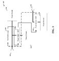
- Fig. 1 shows a power circuit 100 having built-in self test circuits, in accordance with an example embodiment of the present invention.
- the circuit 100 includes power domains 110, 120 and 130, as well as test control logic 140 and daisy-chained BIST switch circuits 150 and 160.
- Arrows 102 and 104 may be implemented as on-chip pads, or on-chip power management units such as an LDO (low-dropout) regulator.
- the test control logic 140 coordinates functions of the respective BIST switch circuits 150 and 160 during testing of the circuits for respectively providing power to power domains 120 and 130.
- the test control logic 140 provides test signals to the BIST switch circuits under various conditions, such as to individually test power switches or subsets of switch circuits within or among different power domains.
- the test control logic 140 is coupled to output test control signals to the BIST switch circuit 150, for use in testing BIST switch circuits 150 and 160.
- the BIST switch circuit 150 is responsive to the received test control signals under a test condition, and outputs test result signals as well test control signals to the BIST switch circuit 160.
- the BIST switch circuit 160 is responsive to the test control signals received from the BIST switch circuit 150 under a test condition, and outputs test result signals for both of the BIST switch circuits 150 and 160 to the test control logic 140. Accordingly, the switch circuits may be tested separately or concurrently, to suit the particular application.
- the test control logic 140 uses the test result signals received from the BIST switch circuit 160 (and also including test result signals from BIST switch circuit 150), to provide an indication of a condition of the respective switch circuits.
- the test control logic 140 may generate signals for testing only one of the BIST switch circuits, passing test signals as above, with result signals from the tested power domain being passed back to the test control logic 140.
- additional BIST switch circuits are connected in daisy-chain fashion as shown and tested, with a last of these circuits connected to provide test results back to the test control logic 140.
- the power circuit 100 facilitates testing of individual switch circuits for respective power domains, while mitigating the need for a large power connection and dedicated pad(s), which can further reduce test time overhead. Accordingly, power capabilities of individual components can be tested and assessed to more accurately represent the ability of the entire circuit 100 to provide power. This approach facilitates desirable testing of less than an entire circuit, as discussed above.
- testing and related functions carried out via the BIST switch circuits 150 and 160 can be implemented using a variety of different types of testing approaches.
- the BIST switch circuits 150 and 160 detect a virtual voltage (or combined voltage), a voltage drop for a specified load (or combined voltage drop), and/or a signal delay such as may occur between enable and acknowledge signals.
- a virtual voltage or combined voltage
- a voltage drop for a specified load or combined voltage drop
- a signal delay such as may occur between enable and acknowledge signals.
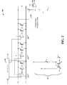
- a power circuit 200 includes built-in self test components with combined power-switch segments, in accordance with another example embodiment of the present invention.
- the power circuit 200 includes a test control block 210, such as a switch control register, which facilitates the control/activation of power-switch segments 220, 230 and 240, which are coupled to power supply V DD and a virtual power supply V VDD .
- Each power-switch segment includes one or more transistors, as represented by transistors 1 - m as shown in switch segment 220, coupled between V DD and V VDD , with corresponding power-switch drivers.
- the test control block 210 provides a select output (TE) to set multiplexers in each power- switch segment to a test mode, which allows the test control block to enable and disable explicit subsets of power-switch segments.
- the test control block 210 also provides test outputs S 1 -S n as inputs (T1) to the multiplexers, with the number n corresponding to n number of power-switch segments.
- the test control block 210 generates different test vectors for different switch segments or clusters of segments, to tailor the testing thereof.
- a current generation circuit 250 acts as a load for testing the power-switch segments 220, 230 and 240, and the output of the power-switch circuits on V VDD is provided to a comparator 260.
- this current generation circuit 250 is used by two or more circuits, acting as the aforesaid load ( e.g ., for other power-switch/built-in-self test blocks).
- the comparator 260 compares the output on V VDD with the output on V DD , and provides an output as an indication of the operability of the one or more of the power-switch segments 220, 230 and 240 operated for the particular test.
- the output of the comparator is stored in a register or other storage circuit, which may be included as part of the power circuit 200.
- the current generation circuit 250 may be implemented in a variety of manners, such as with a current mirror or other current source-type devices (e.g ., as may be similar to a charge pump, variations on current mirrors and other circuits).
- the current generation circuit 250 is implemented as a current mirror-type circuit shown by way of example at 251, and including two NMOS transistors MN1 and MN2, as well as a resistor R ref .
- the ratio of MN1 and MN2 in combination with the resistance of R ref defines the current drawn from the active power-switch segments. Accordingly, these components can be sized and implemented to set a particular current draw, as may be desirable for a particular testing approach.
- a poly resistance can be used to implement the resistor R ref , with a desirably small area, current flowing through MN1 can be set relatively large, and the size of transistor MN2 can be selected such that the desired current is matched to a cluster of power-switch segments to be tested.
- the current generation circuit 250 is configured to draw variable current ( e.g ., by selecting and implementing different transistors), as may be set based upon the number and/or characteristics of power switches to be tested.
- a determination of operability of the power-switch segments can be made based upon a variety of test characteristics and metrics. For example, when the current of an active power-switch segments cluster (e.g ., one of switch segments 220, 230 and 240 operated for a particular test) and current generation circuit are equivalent, the virtual voltage (V VDD ) should be equal or larger than about 0.5 times V DD , with R 1 , R 2 and the respective current generation circuit components configured appropriately. If the output of the comparator 260 is indicative of this ratio, this output is an indication that the clustered power-switch segments passed the test ( e.g ., are operating properly). If the virtual voltage is lower than 0.5 times V DD , the output of the comparator 260 is not indicative of the aforesaid ratio and is indicative of the clustered power-switch segments having failed.
- At least one of the power-switch segments is differently sized relative to another segment, resulting in a different voltage drop introduced by a current generation circuit 251 as shown, since its load is static. Testing of such a circuit may be facilitated using, for example, a dynamic current mirror (e.g ., with different transistors that are switched to provide an appropriate current draw).
- This dynamic current mirror can be created by replacing MN2 of circuit 251 with multiple transistors, which can be enabled individually. These individual current mirror transistors can be linked to the corresponding segment control register to match the current load with the power-switch segment to be tested.
- specific power-switch segments are clustered to create approximately equally sized subsets, which facilitates the use of a single/static current mirror (as the current generation circuit shown in Figure 2 ) to provide the correct load for the subset of power-switch segments.
- Still other implementations are directed to a combination of using a dynamic current mirror and selective clustering, relaxing power-switch segment clustering constraints while limiting the number of individual current mirror transistors.
- Figure 3 shows a flow diagram for testing a power circuit, in accordance with another example embodiment of the present invention.
- the operation of the power circuit as represented in Figure 3 can be made with reference to the operation of a circuit such as that shown in Figure 2 , with the following discussion using such a comparison.
- the approach shown in Figure 3 can be implemented with a variety of different types of circuits and is thus not limited to the circuit shown in Figure 2 or to circuits as otherwise described herein.
- a segment window (X, by way of example) is enabled for testing a particular segment.
- the test enable (TE) signal can be implemented as a global signal used over an entire chip, with the enable (ENA) controlling local test circuitry (e.g ., current mirror, reference voltage, and comparator).
- the segment window X represents a control signal for power-switch segments such as 220, 230 and 240, with each group having its own control signal. When the power-switch segment window is enabled, virtual voltage (V VDD ) will charge, and dependent on the current load, reach a certain value.
- V VDD virtual voltage
- segment window X After segment window X has been tested, the segment window is disabled at block 350. If the last segment in the power circuit has been tested at block 360, the test mode is disabled at block 370, and the test is complete. If the last segment has not been tested at block 360, the segment number X is increased at block 365 to denote a next segment, and the process repeats with this next segment at block 320. At the end of the whole procedure, this fault register represents the power-switch status. At the end of the process (at block 370), if all bits are 0, no error is detected. If one or more bits are 1, a malfunction in the represented segment window is detected.
- an integrated circuit includes a spare power supply circuit, and is configured to route power supply from a power supply circuit detected as exhibiting a failure, via the spare power supply circuit.
- Example applications include microcontrollers for e-metering, hearing aids, wireless sensor networks and integrated circuits for mobile applications.
Landscapes
- Physics & Mathematics (AREA)
- Engineering & Computer Science (AREA)
- Computer Hardware Design (AREA)
- Computing Systems (AREA)
- General Engineering & Computer Science (AREA)
- Mathematical Physics (AREA)
- Tests Of Electronic Circuits (AREA)
- Semiconductor Integrated Circuits (AREA)
Abstract
Description
- Many integrated circuits employ power switches for a variety of uses, such as for providing various power levels, different power domains, and other functions for integrated circuits. In many applications, multiple power domains are often used to reduce leakage current by shutting down the power supply to unused circuit modules using a power switch.
- As the complexity of such integrated circuits increases, multiple power switches are often implemented. Generally, power switches connect the power domain with a supply if active operation is required, and disconnect the domain if active operation is not required (e.g., for standby mode). The power switches are often controlled using a control signal, which can be implemented using a digital control signal (e.g., for mixed-signal devices).
- With increasing numbers of power switches and related complexity, the complexity of testing such circuits increases as well. For example, identifying the supply voltage of each power domain for testing can be particularly challenging to implement in an efficient and economical manner. In addition, certain power testing approaches require dedicated pads, and involve connections that may introduce undesirable resistance and related voltage drop that affect testing measurements, and involve additional overhead. Certain such approaches are also difficult to implement in connection with the use of external power loads.
- These and other matters have presented challenges to the implementation of power switches for controlling different power domains in an integrated circuit chip.
- Various example embodiments are directed to power supply, to testing power domains within power supply circuitry, and to addressing various challenges including those discussed above.
- According to an example embodiment, a power-switch apparatus includes a plurality of individual power switches coupled between a voltage supply and a switched voltage output, a test control circuit, a current generation circuit and an output circuit. The test control circuit is coupled to each of the power switches and operates at least one of the power switches in an "ON" condition for providing the switched voltage output, in response to a test signal received at the at least one of the power switches, while operating at least another one of the respective power switches in an off condition. The current generation circuit is coupled to the switched voltage output and emulates an expected current draw for the respective power switches. The output circuit is coupled to receive the switched voltage output, compare a value of the switched voltage output to a reference value, and provide a test output indicative of an operational characteristic of the power switches operated in the on condition, based on the comparison.
- Another example embodiment is directed to method for testing a power-switch apparatus having a plurality of power switches coupled between a voltage supply and a switched voltage output. At least one of the power switches is operated in an on condition for providing the switched voltage output, in response to a test signal received at the at least one of the power switches, while operating at least another one of the respective power switches in an off condition. An expected current draw for the respective power switches is emulated from the switched voltage output. A value of the switched voltage output is compared to a reference value and, in response to the comparison, a test output is provided to indicate an operational characteristic of the power switches operated in the on condition.
- The above discussion is not intended to describe each embodiment or every implementation of the present disclosure. The figures and following description also exemplify various embodiments.
- Various example embodiments may be more completely understood in consideration of the following detailed description in connection with the accompanying drawings, in which:
-
Fig. 1 shows a power circuit having built-in self-test circuits, in accordance with an example embodiment of the present invention; -
Fig. 2 shows a power circuit with built-in self-test components, in accordance with another example embodiment of the present invention; and -
Fig. 3 shows a flow diagram for testing a power circuit, in accordance with another example embodiment of the present invention. - While the invention is amenable to various modifications and alternative forms, specifics thereof have been shown by way of example in the drawings and will be described in detail. It should be understood, however, that the intention is not to limit the invention to the particular embodiments described. On the contrary, the intention is to cover all modifications, equivalents, and alternatives falling within the scope of the invention, including aspects defined in the claims.
- The present invention is believed to be applicable to a variety of different types of circuits, devices and systems for providing power to integrated circuits, and for testing power switches used in providing power. While the present invention is not necessarily limited in this context, various aspects of the invention may be appreciated through a discussion of related examples.
- In accordance with various example embodiments, an on-chip power-switch testing approach involves verifying aspects, such as supply voltage and IR drop, of a subset of power supply circuits during a specified load for power supply circuitry. In many applications, such an approach involves testing individual segments of a power-switching circuit, with each segment including at least one individual (power) switch, to determine characteristics of each portion as well as the entire power-switching circuit. This segment-based approach can be implemented with one or a group of segments, to suit particular applications. For example, the virtual supply voltage of each segment can be identified along with the voltage drop (e.g., IR drop) of the related power switch (or switches) for a specified current load, which can be an artificial load. The identified supply voltage and IR drop can be used to provide an indication of performance of each switch. Various implementations are also directed to testing power supply using various related parameters, such as wake-up time.
- Where individual switch or circuit performance is not necessarily ascertained, test results from an entire circuit (or large groups of individual switching circuits) can be provided. By ascertaining information regarding circuit functionality for individual circuits or a subset of circuits, an evaluation of the health of an entire circuit (and, e.g., expected longevity) can be more accurately ascertained. For example, in power circuits with a large number of individual components, variations in an output of the entire system may not be indicative of a failure of individual components that do not significantly contribute to the total output. Moreover, by testing less than an entire circuit, smaller power supply lines can be used as each individual circuit or subsets of individual circuits draw less power than the entire circuit.
- In some implementations, individual power-switch circuits are tested using a virtual power supply, with a current generation circuit (e.g., a current mirror) between the virtual supply and the ground as a current load. The virtual supply from the respective power circuits (e.g., a voltage corresponding to an input voltage switched by the power circuits) is fed to a voltage comparator and compared to a voltage reference from an actual power supply. The output of the voltage comparator is indicative of functionality of a power-switch circuit, or a subset of power-switch circuits, that are coupled to the virtual supply and provide an output to the comparator. The output of the comparator is provided (e.g., to a test control unit and/or further test logic) as an indication of the functionality of a power-switch circuit or subset thereof.
- A variety of different types of power switches can be used and/or tested, in accordance with various example embodiments. For example, the size of a power switch can be set in response to a design maximum current consumption of a power domain to be switched, and can be implemented using multiple daisy-chained segments. In such an example, the acknowledge output of a first power switch can be connected to the enable input of a second power switch, and so on through the chain of segments. In order to switch a power-gated domain from standby to active, the power switch is turned on first, and the domain is charged to a supply voltage (VDD) that is set as required for the particular application. Such a power-switch segment can be used in different manners, such as for connecting one or both of a VDD rail and a ground rail. Accordingly, the various examples herein describing the connection (and disconnection) of a VDD rail can be implemented with a ground rail (or other rail, such as a standby power rail).
- Turning now to the figures,
Fig. 1 shows apower circuit 100 having built-in self test circuits, in accordance with an example embodiment of the present invention. Thecircuit 100 includespower domains test control logic 140 and daisy-chainedBIST switch circuits Arrows test control logic 140 coordinates functions of the respectiveBIST switch circuits power domains test control logic 140 provides test signals to the BIST switch circuits under various conditions, such as to individually test power switches or subsets of switch circuits within or among different power domains. - Specifically, the
test control logic 140 is coupled to output test control signals to theBIST switch circuit 150, for use in testingBIST switch circuits BIST switch circuit 150 is responsive to the received test control signals under a test condition, and outputs test result signals as well test control signals to theBIST switch circuit 160. TheBIST switch circuit 160 is responsive to the test control signals received from theBIST switch circuit 150 under a test condition, and outputs test result signals for both of theBIST switch circuits test control logic 140. Accordingly, the switch circuits may be tested separately or concurrently, to suit the particular application. - The
test control logic 140 uses the test result signals received from the BIST switch circuit 160 (and also including test result signals from BIST switch circuit 150), to provide an indication of a condition of the respective switch circuits. In certain implementations, thetest control logic 140 may generate signals for testing only one of the BIST switch circuits, passing test signals as above, with result signals from the tested power domain being passed back to thetest control logic 140. In other implementations, additional BIST switch circuits are connected in daisy-chain fashion as shown and tested, with a last of these circuits connected to provide test results back to thetest control logic 140. - Using such BIST components, the
power circuit 100 facilitates testing of individual switch circuits for respective power domains, while mitigating the need for a large power connection and dedicated pad(s), which can further reduce test time overhead. Accordingly, power capabilities of individual components can be tested and assessed to more accurately represent the ability of theentire circuit 100 to provide power. This approach facilitates desirable testing of less than an entire circuit, as discussed above. - Testing and related functions carried out via the
BIST switch circuits BIST switch circuits - In a more particular example embodiment, and referring to
Figure 2 , apower circuit 200 includes built-in self test components with combined power-switch segments, in accordance with another example embodiment of the present invention. Thepower circuit 200 includes atest control block 210, such as a switch control register, which facilitates the control/activation of power-switch segments - Each power-switch segment includes one or more transistors, as represented by transistors 1 - m as shown in
switch segment 220, coupled between VDD and VVDD, with corresponding power-switch drivers. Thetest control block 210 provides a select output (TE) to set multiplexers in each power- switch segment to a test mode, which allows the test control block to enable and disable explicit subsets of power-switch segments. The test control block 210 also provides test outputs S1-Sn as inputs (T1) to the multiplexers, with the number n corresponding to n number of power-switch segments. In various implementations, thetest control block 210 generates different test vectors for different switch segments or clusters of segments, to tailor the testing thereof. - A
current generation circuit 250 acts as a load for testing the power-switch segments comparator 260. In some implementations, thiscurrent generation circuit 250 is used by two or more circuits, acting as the aforesaid load (e.g., for other power-switch/built-in-self test blocks). Thecomparator 260 compares the output on VVDD with the output on VDD, and provides an output as an indication of the operability of the one or more of the power-switch segments power circuit 200. - The
current generation circuit 250 may be implemented in a variety of manners, such as with a current mirror or other current source-type devices (e.g., as may be similar to a charge pump, variations on current mirrors and other circuits). In some implementations, thecurrent generation circuit 250 is implemented as a current mirror-type circuit shown by way of example at 251, and including two NMOS transistors MN1 and MN2, as well as a resistor Rref. The ratio of MN1 and MN2 in combination with the resistance of Rref defines the current drawn from the active power-switch segments. Accordingly, these components can be sized and implemented to set a particular current draw, as may be desirable for a particular testing approach. For example, a poly resistance can be used to implement the resistor Rref, with a desirably small area, current flowing through MN1 can be set relatively large, and the size of transistor MN2 can be selected such that the desired current is matched to a cluster of power-switch segments to be tested. In some implementations, thecurrent generation circuit 250 is configured to draw variable current (e.g., by selecting and implementing different transistors), as may be set based upon the number and/or characteristics of power switches to be tested. - A determination of operability of the power-switch segments can be made based upon a variety of test characteristics and metrics. For example, when the current of an active power-switch segments cluster (e.g., one of
switch segments comparator 260 is indicative of this ratio, this output is an indication that the clustered power-switch segments passed the test (e.g., are operating properly). If the virtual voltage is lower than 0.5 times VDD, the output of thecomparator 260 is not indicative of the aforesaid ratio and is indicative of the clustered power-switch segments having failed. - In various embodiments, and referring again to
Figure 2 by way of example, at least one of the power-switch segments is differently sized relative to another segment, resulting in a different voltage drop introduced by acurrent generation circuit 251 as shown, since its load is static. Testing of such a circuit may be facilitated using, for example, a dynamic current mirror (e.g., with different transistors that are switched to provide an appropriate current draw). This dynamic current mirror can be created by replacing MN2 ofcircuit 251 with multiple transistors, which can be enabled individually. These individual current mirror transistors can be linked to the corresponding segment control register to match the current load with the power-switch segment to be tested. In another implementation, specific power-switch segments are clustered to create approximately equally sized subsets, which facilitates the use of a single/static current mirror (as the current generation circuit shown inFigure 2 ) to provide the correct load for the subset of power-switch segments. Still other implementations are directed to a combination of using a dynamic current mirror and selective clustering, relaxing power-switch segment clustering constraints while limiting the number of individual current mirror transistors. -
Figure 3 shows a flow diagram for testing a power circuit, in accordance with another example embodiment of the present invention. The operation of the power circuit as represented inFigure 3 can be made with reference to the operation of a circuit such as that shown inFigure 2 , with the following discussion using such a comparison. However, it should be understood that the approach shown inFigure 3 can be implemented with a variety of different types of circuits and is thus not limited to the circuit shown inFigure 2 or to circuits as otherwise described herein. - Upon start, a test mode is enabled at
block 310, with output TE=1, ENA=1 and X=1. Atblock 320, a segment window (X, by way of example) is enabled for testing a particular segment. The test enable (TE) signal can be implemented as a global signal used over an entire chip, with the enable (ENA) controlling local test circuitry (e.g., current mirror, reference voltage, and comparator). The segment window X represents a control signal for power-switch segments such as 220, 230 and 240, with each group having its own control signal. When the power-switch segment window is enabled, virtual voltage (VVDD) will charge, and dependent on the current load, reach a certain value. - In one embodiment, the current load is selected to equal the power-switch segment window load, resulting in VVDD=VDD/2 (with the switches operating properly). Accordingly, Vref is selected to be equal to VDD/2. If the VVDD is larger than or equal to Vref at
block 330, the power-switch segments being tested are determined as operating as specified, and fault bit X is cleared atblock 340. However, ifVVDD is smaller than Vref atblock 330, the power-switch segments in the current window are determined as not operating as specified and the fault bit X is set atblock 335. - After segment window X has been tested, the segment window is disabled at
block 350. If the last segment in the power circuit has been tested atblock 360, the test mode is disabled atblock 370, and the test is complete. If the last segment has not been tested atblock 360, the segment number X is increased atblock 365 to denote a next segment, and the process repeats with this next segment atblock 320. At the end of the whole procedure, this fault register represents the power-switch status. At the end of the process (at block 370), if all bits are 0, no error is detected. If one or more bits are 1, a malfunction in the represented segment window is detected. - The testing circuits and approach as discussed herein thus may, for example, be implemented as part of a manufacturing process to detect failed power switches as an indication of an expected longevity of a particular power-switch circuit involving a plurality of such switches. This approach may also be implemented during implementation of the power-switch circuit, to predict failure and/or suggest replacement. In one particular implementation, an integrated circuit includes a spare power supply circuit, and is configured to route power supply from a power supply circuit detected as exhibiting a failure, via the spare power supply circuit.
- The various embodiments as described herein can be implemented using one or more of a variety of approaches, in a variety of different applications. For example, individual power switches, or segments/blocks of power switches, can be used in power gating for an integrated circuit, and tested as discussed herein. Example applications include microcontrollers for e-metering, hearing aids, wireless sensor networks and integrated circuits for mobile applications.
- Based upon the above discussion and illustrations, those skilled in the art will readily recognize that various modifications and changes may be made to the present invention without strictly following the exemplary embodiments and applications illustrated and described herein. For example, dynamic current mirrors may be implemented in place of static current mirrors, and different sets of switches can be grouped. Further, test signals and control signals may be provided in different manners and implemented to achieve the indicated operation of individual and/or subsets of switches. Such modifications do not depart from the true spirit and scope of the present invention, including that set forth in the following claims. Furthermore, the term "example" as used throughout this document is by way of illustration, and not limitation.
Claims (12)
- A power-switch apparatus comprising:a plurality of power-switching circuits coupled between a voltage supply and a switched voltage output;a test control circuit coupled to each of the power-switching circuits and configured and arranged to operate at least one of the power-switching circuits in an on condition for providing the switched voltage output, in response to a test signal received at the at least one of the power-switching circuits, while operating at least another one of the respective power-switching circuits in an off condition;a current generation circuit coupled to the switched voltage output and configured and arranged to emulate an expected current draw for the respective power-switching circuits;an output circuit coupled to receive the switched voltage output and configured and arranged to
compare a value of the switched voltage output to a reference value, and
in response to the comparison, provide a test output indicative of an operational characteristic of the power-switching circuits operated in the on condition. - The apparatus of claim 1, wherein the test control circuit is configured and arranged to operate different subsets of the power-switching circuits in the on condition during different test cycles to separately test each of the respective subsets relative to the other subsets in respective ones of the test cycles.
- The apparatus of claim 1, wherein
different subsets of the power-switching circuits draw different power levels,
the test control circuit is configured and arranged to operate the different subsets of the power-switching circuits in the on condition during different test cycles to separately test each of the respective subsets relative to the other subsets in respective ones of the test cycles, and
the current generation circuit is a dynamic current mirror circuit configured and arranged to respond to the test control circuit by providing a current draw corresponding to the particular subset of power-switching circuits being tested. - The apparatus of claim 1, wherein
different ones of the power-switching circuits draw different power levels,
the test control circuit is configured and arranged to combine different ones of the power-switching circuits into respective subsets to create subsets exhibiting an about equal current draw. - The apparatus of claim 1, wherein
different ones of the power-switching circuits draw different power levels,
the test control circuit is configured and arranged to combine different ones of the power-switching circuits into respective subsets to create subsets exhibiting an about equal current draw,
the test control circuit is configured and arranged to operate the different subsets of the power-switching circuits in the on condition during different test cycles to separately test each of the respective subsets relative to the other subsets in respective ones of the test cycles, and
the current generation circuit is a dynamic current mirror circuit configured and arranged to respond to the test control circuit by providing a current draw corresponding to the particular subsets being tested. - The apparatus of claim 1, wherein the test control circuit is configured and arranged to provide the test signals to each switch.
- The apparatus of claim 1, wherein the power-switching circuits, test control circuit, current generation circuit and output circuit are integrated on a common integrated circuit chip.
- The apparatus of claim 1, wherein the current generation circuit is coupled to a switched voltage output for a different plurality of power-switching circuits, and configured and arranged to emulate an expected current draw for the different plurality of power-switching circuits.
- The apparatus of claim 1, wherein
the power-switching circuits, test control circuit, current generation circuit and output circuit are integrated on a common integrated circuit chip,
the current generation circuit is configured and arranged to emulate an expected off-chip current load, and
the output circuit includes a comparator that compares the value of the switched voltage output to the reference value by comparing the switch voltage output to a reference voltage provided via the voltage supply. - The apparatus of claim 1, wherein the output circuit is configured to set an output corresponding to at least one of the power-switching circuits tested in a test cycle, based upon the comparison of the value of the switched voltage output to the reference value, to provide an indication of the operability of the at least one of the power-switching circuits.
- The apparatus of claim 1, wherein the test control circuit is configured and arranged to
separately test different groups of the power-switching circuits, and
process the test output as provided for each group of power-switching circuits to provide an indication of operability of each group of power-switching circuits within the power-switch apparatus. - The apparatus of claim 1, wherein the test control circuit is configured and arranged to generate different test vectors for operating different subsets of the power-switching circuits under a specified load configuration.
Applications Claiming Priority (1)
| Application Number | Priority Date | Filing Date | Title |
|---|---|---|---|
| US13/208,819 US9100001B2 (en) | 2011-08-12 | 2011-08-12 | Power-switch test apparatus and method |
Publications (2)
| Publication Number | Publication Date |
|---|---|
| EP2557691A2 true EP2557691A2 (en) | 2013-02-13 |
| EP2557691A3 EP2557691A3 (en) | 2013-12-25 |
Family
ID=47115197
Family Applications (1)
| Application Number | Title | Priority Date | Filing Date |
|---|---|---|---|
| EP12178245.2A Ceased EP2557691A3 (en) | 2011-08-12 | 2012-07-27 | Power switch test apparatus and method |
Country Status (3)
| Country | Link |
|---|---|
| US (1) | US9100001B2 (en) |
| EP (1) | EP2557691A3 (en) |
| CN (1) | CN102955128A (en) |
Families Citing this family (8)
| Publication number | Priority date | Publication date | Assignee | Title |
|---|---|---|---|---|
| US20140172343A1 (en) * | 2012-12-13 | 2014-06-19 | Infineon Technologies Ag | Emulation System and Method |
| CN104678240B (en) * | 2013-12-03 | 2019-03-29 | 恩智浦美国有限公司 | For testing the circuit of power supply in multiple power modes |
| CN103995227B (en) * | 2014-05-14 | 2016-06-01 | 国家电网公司 | The planned state test method of distribution switch |
| US9678111B2 (en) * | 2015-10-07 | 2017-06-13 | Nxp B.V. | Current sensing with compensation for component variations |
| WO2017096520A1 (en) * | 2015-12-08 | 2017-06-15 | Qualcomm Incorporated | Hierarchical power domain organization |
| US11204384B1 (en) | 2018-09-21 | 2021-12-21 | Apple Inc. | Methods and systems for switchable logic to recover integrated circuits with short circuits |
| US10915157B2 (en) * | 2019-02-14 | 2021-02-09 | Qualcomm Incorporated | Dynamic power switch control scheme |
| US11119153B1 (en) * | 2020-05-29 | 2021-09-14 | Stmicroelectronics International N.V. | Isolation enable test coverage for multiple power domains |
Family Cites Families (7)
| Publication number | Priority date | Publication date | Assignee | Title |
|---|---|---|---|---|
| JP3203996B2 (en) * | 1994-11-01 | 2001-09-04 | 三菱電機株式会社 | Test circuit for current-voltage conversion amplifier |
| JP2003532082A (en) | 2000-04-26 | 2003-10-28 | コーニンクレッカ フィリップス エレクトロニクス エヌ ヴィ | Electronic circuit device with short-circuit switch and method for testing the device |
| US6798286B2 (en) | 2002-12-02 | 2004-09-28 | Broadcom Corporation | Gain control methods and systems in an amplifier assembly |
| JP2006170878A (en) | 2004-12-17 | 2006-06-29 | Sony Corp | Electronic circuit device and measuring method thereof |
| EP1977262A2 (en) * | 2006-01-09 | 2008-10-08 | Nxp B.V. | Testable integrated circuit and ic test method |
| US7868640B2 (en) * | 2008-04-02 | 2011-01-11 | International Business Machines Corporation | Array-based early threshold voltage recovery characterization measurement |
| US7675308B1 (en) | 2008-08-20 | 2010-03-09 | Faraday Technology Corp. | Test circuit and test method for power switch |
-
2011
- 2011-08-12 US US13/208,819 patent/US9100001B2/en active Active
-
2012
- 2012-07-27 EP EP12178245.2A patent/EP2557691A3/en not_active Ceased
- 2012-08-08 CN CN2012102805519A patent/CN102955128A/en active Pending
Non-Patent Citations (1)
| Title |
|---|
| None |
Also Published As
| Publication number | Publication date |
|---|---|
| EP2557691A3 (en) | 2013-12-25 |
| US9100001B2 (en) | 2015-08-04 |
| US20130038361A1 (en) | 2013-02-14 |
| CN102955128A (en) | 2013-03-06 |
Similar Documents
| Publication | Publication Date | Title |
|---|---|---|
| US9100001B2 (en) | Power-switch test apparatus and method | |
| US6744151B2 (en) | Multi-channel power supply selector | |
| US9103891B2 (en) | Voltage monitoring circuit, test method therefor, and voltage monitoring system | |
| US9151804B2 (en) | On-chip test technique for low drop-out regulators | |
| US9081069B2 (en) | Protection IC and method of monitoring a battery voltage | |
| EP2219281A2 (en) | Circuit and method for cell balancing | |
| US20210231746A1 (en) | Apparatus and method to debug a voltage regulator | |
| US8847665B2 (en) | Semiconductor device and method of controlling analog switch | |
| US10620267B2 (en) | Circuitry for testing non-maskable voltage monitor for power management block | |
| US20180031635A1 (en) | Methods for switch health determination | |
| US20210148968A1 (en) | Self-test circuitry | |
| KR102006023B1 (en) | Apparatus for testing a semiconductor device | |
| KR102830363B1 (en) | Voltage level detecter performing state detection | |
| US20190366849A1 (en) | Self-test circuit, and corresponding device, vehicle and method | |
| JP2009523229A (en) | Testable integrated circuit and IC test method | |
| CN112713754B (en) | Driver circuit, system with driver circuit, and method for calibrating driver circuit | |
| US10122185B2 (en) | Battery management system | |
| KR20180127776A (en) | Semiconductor apparatus including power gating circuit and repair method thereof | |
| KR102044808B1 (en) | Battery control system and driving method of the same | |
| US9945888B2 (en) | On-die measurement technique for I/O DC parameters VOL and VOH | |
| JP2019168309A (en) | Integrated circuit | |
| US9362904B2 (en) | Devices and method for testing power-on reset voltage | |
| JP2011512751A (en) | Differential current output driver with overvoltage protection | |
| US12553940B2 (en) | Method and apparatus for detecting power-on reset threshold | |
| CA3038145C (en) | Power management integrated circuit |
Legal Events
| Date | Code | Title | Description |
|---|---|---|---|
| PUAI | Public reference made under article 153(3) epc to a published international application that has entered the european phase |
Free format text: ORIGINAL CODE: 0009012 |
|
| AK | Designated contracting states |
Kind code of ref document: A2 Designated state(s): AL AT BE BG CH CY CZ DE DK EE ES FI FR GB GR HR HU IE IS IT LI LT LU LV MC MK MT NL NO PL PT RO RS SE SI SK SM TR |
|
| AX | Request for extension of the european patent |
Extension state: BA ME |
|
| RIN1 | Information on inventor provided before grant (corrected) |
Inventor name: GROOT, CAS Inventor name: MEIJER, RINZE |
|
| PUAL | Search report despatched |
Free format text: ORIGINAL CODE: 0009013 |
|
| AK | Designated contracting states |
Kind code of ref document: A3 Designated state(s): AL AT BE BG CH CY CZ DE DK EE ES FI FR GB GR HR HU IE IS IT LI LT LU LV MC MK MT NL NO PL PT RO RS SE SI SK SM TR |
|
| AX | Request for extension of the european patent |
Extension state: BA ME |
|
| RIC1 | Information provided on ipc code assigned before grant |
Ipc: G01R 31/3187 20060101ALI20131118BHEP Ipc: H03K 19/00 20060101AFI20131118BHEP |
|
| 17P | Request for examination filed |
Effective date: 20140331 |
|
| RBV | Designated contracting states (corrected) |
Designated state(s): AL AT BE BG CH CY CZ DE DK EE ES FI FR GB GR HR HU IE IS IT LI LT LU LV MC MK MT NL NO PL PT RO RS SE SI SK SM TR |
|
| 17Q | First examination report despatched |
Effective date: 20150921 |
|
| STAA | Information on the status of an ep patent application or granted ep patent |
Free format text: STATUS: THE APPLICATION HAS BEEN REFUSED |
|
| 18R | Application refused |
Effective date: 20171103 |