EP2557596A2 - Display device - Google Patents
Display device Download PDFInfo
- Publication number
- EP2557596A2 EP2557596A2 EP12178549A EP12178549A EP2557596A2 EP 2557596 A2 EP2557596 A2 EP 2557596A2 EP 12178549 A EP12178549 A EP 12178549A EP 12178549 A EP12178549 A EP 12178549A EP 2557596 A2 EP2557596 A2 EP 2557596A2
- Authority
- EP
- European Patent Office
- Prior art keywords
- layer
- display device
- base film
- active layer
- laser
- Prior art date
- Legal status (The legal status is an assumption and is not a legal conclusion. Google has not performed a legal analysis and makes no representation as to the accuracy of the status listed.)
- Granted
Links
Images


Classifications
-
- H—ELECTRICITY
- H10—SEMICONDUCTOR DEVICES; ELECTRIC SOLID-STATE DEVICES NOT OTHERWISE PROVIDED FOR
- H10D—INORGANIC ELECTRIC SEMICONDUCTOR DEVICES
- H10D86/00—Integrated devices formed in or on insulating or conducting substrates, e.g. formed in silicon-on-insulator [SOI] substrates or on stainless steel or glass substrates
- H10D86/40—Integrated devices formed in or on insulating or conducting substrates, e.g. formed in silicon-on-insulator [SOI] substrates or on stainless steel or glass substrates characterised by multiple TFTs
- H10D86/411—Integrated devices formed in or on insulating or conducting substrates, e.g. formed in silicon-on-insulator [SOI] substrates or on stainless steel or glass substrates characterised by multiple TFTs characterised by materials, geometry or structure of the substrates
-
- G—PHYSICS
- G02—OPTICS
- G02F—OPTICAL DEVICES OR ARRANGEMENTS FOR THE CONTROL OF LIGHT BY MODIFICATION OF THE OPTICAL PROPERTIES OF THE MEDIA OF THE ELEMENTS INVOLVED THEREIN; NON-LINEAR OPTICS; FREQUENCY-CHANGING OF LIGHT; OPTICAL LOGIC ELEMENTS; OPTICAL ANALOGUE/DIGITAL CONVERTERS
- G02F1/00—Devices or arrangements for the control of the intensity, colour, phase, polarisation or direction of light arriving from an independent light source, e.g. switching, gating or modulating; Non-linear optics
- G02F1/01—Devices or arrangements for the control of the intensity, colour, phase, polarisation or direction of light arriving from an independent light source, e.g. switching, gating or modulating; Non-linear optics for the control of the intensity, phase, polarisation or colour
- G02F1/13—Devices or arrangements for the control of the intensity, colour, phase, polarisation or direction of light arriving from an independent light source, e.g. switching, gating or modulating; Non-linear optics for the control of the intensity, phase, polarisation or colour based on liquid crystals, e.g. single liquid crystal display cells
- G02F1/133—Constructional arrangements; Operation of liquid crystal cells; Circuit arrangements
- G02F1/1333—Constructional arrangements; Manufacturing methods
- G02F1/133305—Flexible substrates, e.g. plastics, organic film
-
- H—ELECTRICITY
- H10—SEMICONDUCTOR DEVICES; ELECTRIC SOLID-STATE DEVICES NOT OTHERWISE PROVIDED FOR
- H10D—INORGANIC ELECTRIC SEMICONDUCTOR DEVICES
- H10D86/00—Integrated devices formed in or on insulating or conducting substrates, e.g. formed in silicon-on-insulator [SOI] substrates or on stainless steel or glass substrates
- H10D86/01—Manufacture or treatment
- H10D86/021—Manufacture or treatment of multiple TFTs
- H10D86/0212—Manufacture or treatment of multiple TFTs comprising manufacture, treatment or coating of substrates
-
- H—ELECTRICITY
- H10—SEMICONDUCTOR DEVICES; ELECTRIC SOLID-STATE DEVICES NOT OTHERWISE PROVIDED FOR
- H10D—INORGANIC ELECTRIC SEMICONDUCTOR DEVICES
- H10D86/00—Integrated devices formed in or on insulating or conducting substrates, e.g. formed in silicon-on-insulator [SOI] substrates or on stainless steel or glass substrates
- H10D86/01—Manufacture or treatment
- H10D86/021—Manufacture or treatment of multiple TFTs
- H10D86/0221—Manufacture or treatment of multiple TFTs comprising manufacture, treatment or patterning of TFT semiconductor bodies
-
- H—ELECTRICITY
- H10—SEMICONDUCTOR DEVICES; ELECTRIC SOLID-STATE DEVICES NOT OTHERWISE PROVIDED FOR
- H10D—INORGANIC ELECTRIC SEMICONDUCTOR DEVICES
- H10D86/00—Integrated devices formed in or on insulating or conducting substrates, e.g. formed in silicon-on-insulator [SOI] substrates or on stainless steel or glass substrates
- H10D86/01—Manufacture or treatment
- H10D86/021—Manufacture or treatment of multiple TFTs
- H10D86/0221—Manufacture or treatment of multiple TFTs comprising manufacture, treatment or patterning of TFT semiconductor bodies
- H10D86/0223—Manufacture or treatment of multiple TFTs comprising manufacture, treatment or patterning of TFT semiconductor bodies comprising crystallisation of amorphous, microcrystalline or polycrystalline semiconductor materials
- H10D86/0227—Manufacture or treatment of multiple TFTs comprising manufacture, treatment or patterning of TFT semiconductor bodies comprising crystallisation of amorphous, microcrystalline or polycrystalline semiconductor materials using structural arrangements to control crystal growth, e.g. placement of grain filters
-
- H—ELECTRICITY
- H10—SEMICONDUCTOR DEVICES; ELECTRIC SOLID-STATE DEVICES NOT OTHERWISE PROVIDED FOR
- H10D—INORGANIC ELECTRIC SEMICONDUCTOR DEVICES
- H10D86/00—Integrated devices formed in or on insulating or conducting substrates, e.g. formed in silicon-on-insulator [SOI] substrates or on stainless steel or glass substrates
- H10D86/40—Integrated devices formed in or on insulating or conducting substrates, e.g. formed in silicon-on-insulator [SOI] substrates or on stainless steel or glass substrates characterised by multiple TFTs
- H10D86/60—Integrated devices formed in or on insulating or conducting substrates, e.g. formed in silicon-on-insulator [SOI] substrates or on stainless steel or glass substrates characterised by multiple TFTs wherein the TFTs are in active matrices
-
- H—ELECTRICITY
- H10—SEMICONDUCTOR DEVICES; ELECTRIC SOLID-STATE DEVICES NOT OTHERWISE PROVIDED FOR
- H10K—ORGANIC ELECTRIC SOLID-STATE DEVICES
- H10K77/00—Constructional details of devices covered by this subclass and not covered by groups H10K10/80, H10K30/80, H10K50/80 or H10K59/80
- H10K77/10—Substrates, e.g. flexible substrates
- H10K77/111—Flexible substrates
-
- H—ELECTRICITY
- H10—SEMICONDUCTOR DEVICES; ELECTRIC SOLID-STATE DEVICES NOT OTHERWISE PROVIDED FOR
- H10K—ORGANIC ELECTRIC SOLID-STATE DEVICES
- H10K2102/00—Constructional details relating to the organic devices covered by this subclass
- H10K2102/301—Details of OLEDs
- H10K2102/311—Flexible OLED
-
- Y—GENERAL TAGGING OF NEW TECHNOLOGICAL DEVELOPMENTS; GENERAL TAGGING OF CROSS-SECTIONAL TECHNOLOGIES SPANNING OVER SEVERAL SECTIONS OF THE IPC; TECHNICAL SUBJECTS COVERED BY FORMER USPC CROSS-REFERENCE ART COLLECTIONS [XRACs] AND DIGESTS
- Y02—TECHNOLOGIES OR APPLICATIONS FOR MITIGATION OR ADAPTATION AGAINST CLIMATE CHANGE
- Y02E—REDUCTION OF GREENHOUSE GAS [GHG] EMISSIONS, RELATED TO ENERGY GENERATION, TRANSMISSION OR DISTRIBUTION
- Y02E10/00—Energy generation through renewable energy sources
- Y02E10/50—Photovoltaic [PV] energy
- Y02E10/549—Organic PV cells
Definitions
- the present invention relates generally to a display device. More particularly, the invention relates to a display device using a base film including plastic.
- Different flexible flat display devices may include, for example, organic light emitting diode display elements, liquid crystal display elements, and electrophoretic display (EPD) elements, among others.
- organic light emitting diode display elements liquid crystal display elements
- EPD electrophoretic display
- flexible flat display devices may include thin film transistors (TFTs).
- TFTs thin film transistors
- advantages such as having good carrier mobility, a low temperature polysilicon (LTPS) TFT can be applicable to a high speed operational circuit and can be used for a CMOS circuit, so LTPS TFTS are commonly utilized from among various types of thin film transistors.
- LTPS low temperature polysilicon
- the LTPS TFT includes a polysilicon layer formed by crystallizing an amorphous silicon layer.
- Methods for crystallizing the amorphous silicon layer include, for example, solid phase crystallization, excimer laser crystallization, and crystallization using a metal catalyst.
- the excimer laser crystallization method has been widely used because it allows for low temperature processes, so that a thermal effect on a substrate is relatively low and a polysilicon layer having relatively excellent carrier mobility over 100cm2/Vs can be made.
- the present invention seeks to provide a display device that can stably form an active layer crystallized using a laser on a base film including a material such as plastic.
- a display device therefore includes: a base film including plastic; an active layer on the base film, the active layer including a polysilicon layer formed by crystallizing an amorphous silicon layer using a laser; a barrier layer between the active layer and the base film; and a laser absorption layer between the barrier layer and the active layer.
- the barrier layer may include a plurality of inorganic layers.
- the display device may further include a buffer layer between the laser absorption layer and the active layer.
- the laser absorption layer may include an amorphous silicon layer.
- the active layer may be crystallized through excimer laser annealing (ELA).
- ELA excimer laser annealing
- the base film may include a material including polyimide.
- the barrier layer may include a structure in which silicon oxide layers and silicon nitride layers are alternately layered.
- the buffer layer may include at least one of a tetra ethyl ortho silicate (TEOS) layer, a silicon nitride layer, a silicon oxide layer, and a silicon oxynitride layer.
- TEOS tetra ethyl ortho silicate
- the base film, the barrier layer, the laser absorption layer, and the active layer may be flexible.
- a display device includes: a base film including plastic; an active layer on the base film, the active layer including a polysilicon layer formed by crystallizing an amorphous silicon layer using a laser; a barrier layer between the active layer and the base film, the barrier layer including a plurality of inorganic layers; and a laser absorption layer between two of the plurality of inorganic layers.
- the display device may further include a buffer layer between the barrier layer and the active layer.
- a display can have a stably formed active layer crystallized using a laser on a base film including a material such as plastic.
- FIG. 1 is a cross-sectional view of a display device according to a first embodiment of the invention
- FIG. 2 is an enlarged cross-sectional view of a portion of FIG. 1 ;
- FIG. 3 is a cross-sectional view of a display device according to a second embodiment of the invention.
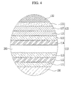
- FIG. 4 is an enlarged cross-sectional view of a portion of FIG. 3 .
- FIG. 1 and FIG. 2 a display device 101 according to a first embodiment of the invention will be described with reference to FIG. 1 and FIG. 2 .
- the display device 101 includes a base film 100, a barrier layer 110, a laser absorption layer 200, a thin film transistor 20, and an organic light emitting element 70.
- the thin film transistor 20 includes an active layer 132, a gate electrode 155, a source electrode 176, and a drain electrode 177.
- the thin film transistor 20 has a top gate structure in which the gate electrode 155 is disposed on the active layer 132.
- the active layer 132 includes a polysilicon layer crystallized from an amorphous silicon layer using a laser.
- the crystallization method using a laser may be, for example, an excimer laser annealing (ELA) method in particular.
- the display device 101 further includes a gate insulating layer 140 for insulating the active layer 132 of the thin film transistor 20 from the gate electrode 155 and an interlayer insulating layer 160 for insulating the gate electrode 155 from the source electrode 176 and the drain electrode 177.
- the organic light emitting element 70 includes a pixel electrode 710 connected to the drain electrode 177 of the thin film transistor 20, an organic emission layer 720 on the pixel electrode 710, and a common electrode 730 on the organic emission layer 720.
- the pixel electrode 710 is a positive (+) electrode, which is a hole injection electrode and the common electrode 730 is a negative (-) electrode, which is an electron injection electrode.
- the invention is not limited thereto, and for example, the pixel electrode 710 may be the negative electrode and the common electrode 730 may be the positive electrode, according to a particular driving method of the display device 101.
- Holes from the pixel electrode 710 and electrons from the common electrode 730 are injected into the organic emission layer 720, and light emission occurs when excitons, which are combinations of holes and electrons, drop from an excited state to a ground state.
- the display device 101 further includes a pixel defining layer 190 having an opening 195 exposing the pixel electrode 710 to define a light emission area.
- the organic emission layer 720 is positioned on the pixel electrode 710 in the opening 195 of the pixel defining layer 190.
- the display device 101 further includes an additional insulating layer 180 for insulating the pixel electrode 710 from the source electrode 176.
- the additional insulating layer 180 in this case has a planarization or planarizing characteristic, so that it can make the organic emission layer 720 substantially uniformly disposed on the pixel electrode 710.
- the structure of the organic light emitting element 70 and the thin film transistor 20 are not limited to the structures shown in FIG. 2 .
- the structures of the organic light emitting element 70 and the thin film transistor 20 may be changed in a variety of ways and can be easily modified by a person skilled in the art.
- the base film 100 is made of or includes a plastic.
- the base film 100 may be made of polyimide having excellent heat resistance, chemical resistance, durability, and electric insulation.
- the invention is not limited thereto, and the base film 100 may be made of, for example, polyethylene etherphtalate, polyethylene naphthalate, polycarbonate, polyarylate, polyetherimide, or polyethersulfone.
- the barrier layer 110 prevents permeation of moisture or oxygen.
- the base film 100 made of plastic is more permeable to moisture or oxygen than a substrate made of glass.
- the barrier layer 110 is positioned on the base film 100 to prevent or reduce moisture or oxygen from permeating past the base film 100 and negatively affecting the organic light emitting element 70 on the base film 100.
- the barrier layer 110 includes a plurality of inorganic layers 111, 112, 113, 114, and 115.
- the barrier layer 110 has a structure in which silicon oxide layers 111, 113, and 115 and silicon nitride layers 112 and 114 are alternately stacked.
- the invention is not limited thereto, and the barrier layer 110 may include various different types of inorganic layers.
- a laser absorption layer 200 prevents or reduces parts of laser beams radiated during a process of forming the active layer 132 of the thin film transistor 20 from passing through the barrier layer 110 toward the base film 100. If the laser beams reach the base film 100, the laser beams can be absorbed by the base film 100, which may deteriorate the base film 100. Therefore, the laser absorption layer 200 prevents the laser beams from reaching the base film 100 by absorbing the laser beams moving toward the base film 100.
- an amorphous silicon layer is used as the laser absorption layer 200.
- the amorphous silicon layer used as the laser absorption layer 200 can be partially crystallized while absorbing the laser beams.
- the buffer layer 120 is arranged on the laser absorption layer 200.
- the buffer layer 120 includes at least one of a tetra ethyl ortho silicate (TEOS) layer, a silicon nitride layer, a silicon oxide layer, or a silicon oxynitride layer.
- FIG. 2 illustrates a tri-layered buffer layer 120 that includes a silicon nitride layer 121, a silicon oxide layer 122, and a TEOS layer 123.
- the buffer layer 120 may be omitted in the display device 101 in some embodiments. However, the buffer layer 120 additionally blocks moisture or oxygen that passed through the barrier layer 110, and also planarizes the surface to stably form the active layer 132.
- the active layer 132 of the thin film transistor 20 is disposed on the buffer layer 120. As described above, the active layer 132 is formed by patterning the polysilicon layer that is formed by crystallizing the amorphous silicon layer using a laser.
- the display device 101 may further include a thin film encapsulation layer 300 covering the organic light emitting element 70.
- the thin film encapsulation layer 300 may have a structure in which at least one of a plurality of inorganic layers and at least one of a plurality of organic layers are layered. Like the base film 100 and the barrier layer 110, the thin film encapsulation layer 300 prevents or reduces permeation of moisture or oxygen into the organic light emitting element 70 while protecting the organic light emitting element 70.
- the display device 101 is not limited to an organic light emitting diode display.
- embodiments of the invention can be applied to any display device that includes a thin film transistor using a polysilicon layer crystallized by a laser.
- Such display devices include, for example, liquid crystal displays and electrophoretic display (EPD) devices.
- the display device 101 can stably form an active layer 132 crystallized using a laser, on a base film 100 made of or including plastic. That is, separation of the base film 100 from a barrier layer 110 caused by deterioration of the base film 100 due to the laser beams during the forming of the active layer 132 can be effectively prevented or reduced.
- a laser absorption layer 200 is disposed in the middle of a barrier layer 110.
- the laser absorption layer 200 is positioned between a plurality of inorganic layers 111, 112, 113, 114, and 115 of the barrier layer 110.
- the barrier layer 110 includes silicon oxide layers 111, 113, and 115 and silicon nitride layers 112 and 114 that are alternately stacked, and the laser absorption layer 200 may be positioned in at least one space between the silicon oxide layers 111, 113, and 115 the silicon nitride layers 112 and 114.
- the display device 102 can also stably form the active layer 132 crystallized using a laser beam, on a base film 100 made of or including plastic. That is, separation of the base film 100 from the barrier layer 110 caused by deterioration of the base film 100 due to the laser beams during the forming of the active layer 132 can be effectively prevented or reduced.
Landscapes
- Physics & Mathematics (AREA)
- Nonlinear Science (AREA)
- Mathematical Physics (AREA)
- Chemical & Material Sciences (AREA)
- Crystallography & Structural Chemistry (AREA)
- General Physics & Mathematics (AREA)
- Optics & Photonics (AREA)
- Electroluminescent Light Sources (AREA)
- Recrystallisation Techniques (AREA)
- Devices For Indicating Variable Information By Combining Individual Elements (AREA)
- Thin Film Transistor (AREA)
- Micromachines (AREA)
Abstract
Description
- The present invention relates generally to a display device. More particularly, the invention relates to a display device using a base film including plastic.
- Recently, flexible flat display devices, which are lightweight and resistant to impact, have been developed by utilizing a base film made of a material such as plastic.
- Different flexible flat display devices may include, for example, organic light emitting diode display elements, liquid crystal display elements, and electrophoretic display (EPD) elements, among others.
- In addition, flexible flat display devices may include thin film transistors (TFTs). With advantages such as having good carrier mobility, a low temperature polysilicon (LTPS) TFT can be applicable to a high speed operational circuit and can be used for a CMOS circuit, so LTPS TFTS are commonly utilized from among various types of thin film transistors.
- The LTPS TFT includes a polysilicon layer formed by crystallizing an amorphous silicon layer. Methods for crystallizing the amorphous silicon layer include, for example, solid phase crystallization, excimer laser crystallization, and crystallization using a metal catalyst. The excimer laser crystallization method has been widely used because it allows for low temperature processes, so that a thermal effect on a substrate is relatively low and a polysilicon layer having relatively excellent carrier mobility over 100cm2/Vs can be made.
- However, when the crystallization process is performed using a laser on a base film made of plastic, laser beams passed through the polysilicon layer are partially absorbed by the base film, thereby causing deterioration of the base film. Such a deterioration of the base film not only causes a negative effect on product reliability, but also causes failures such as separation of the base film.
- The above information disclosed in this Background section is only for enhancement of understanding of the background of the described technology, and therefore, it may contain information that does not form the prior art that is already known in this country to a person of ordinary skill in the art.
- The present invention seeks to provide a display device that can stably form an active layer crystallized using a laser on a base film including a material such as plastic.
- A display device according to an embodiment of the invention therefore includes: a base film including plastic; an active layer on the base film, the active layer including a polysilicon layer formed by crystallizing an amorphous silicon layer using a laser; a barrier layer between the active layer and the base film; and a laser absorption layer between the barrier layer and the active layer.
- The barrier layer may include a plurality of inorganic layers.
- The display device may further include a buffer layer between the laser absorption layer and the active layer.
- The laser absorption layer may include an amorphous silicon layer.
- The active layer may be crystallized through excimer laser annealing (ELA).
- The base film may include a material including polyimide.
- The barrier layer may include a structure in which silicon oxide layers and silicon nitride layers are alternately layered.
- The buffer layer may include at least one of a tetra ethyl ortho silicate (TEOS) layer, a silicon nitride layer, a silicon oxide layer, and a silicon oxynitride layer.
- The base film, the barrier layer, the laser absorption layer, and the active layer may be flexible.
- A display device according to another embodiment includes: a base film including plastic; an active layer on the base film, the active layer including a polysilicon layer formed by crystallizing an amorphous silicon layer using a laser; a barrier layer between the active layer and the base film, the barrier layer including a plurality of inorganic layers; and a laser absorption layer between two of the plurality of inorganic layers.
- The display device may further include a buffer layer between the barrier layer and the active layer.
- According to embodiments of the present invention, a display can have a stably formed active layer crystallized using a laser on a base film including a material such as plastic.
- At lest some of the above and other features of the invention are set out in the claims.
-
FIG. 1 is a cross-sectional view of a display device according to a first embodiment of the invention; -
FIG. 2 is an enlarged cross-sectional view of a portion ofFIG. 1 ; -
FIG. 3 is a cross-sectional view of a display device according to a second embodiment of the invention; and -
FIG. 4 is an enlarged cross-sectional view of a portion ofFIG. 3 . - The present invention will be described more fully hereinafter with reference to the accompanying drawings, in which certain embodiments of the invention are shown. As those skilled in the art will recognize, the described embodiments may be modified in various different ways without departing from the scope of the present invention.
- Elements having the same or similar structures throughout the embodiments are denoted by the same reference numerals and are described in detail for a first embodiment. In subsequent embodiments, only the elements other than the same or similar elements will be described.
- The drawings are schematic and not proportionally scaled. Relative scales and ratios in the drawings are enlarged or reduced for the purpose of convenience, and the scales may be random and the invention should not be limited thereto. In addition, it will be understood that when an element is referred to as being "on" another element, it can be directly on the other element, or one or more intervening elements may be present therebetween.
- The embodiments described include details that are not essential to the invention. Therefore, various modifications from them are to be expected. Accordingly, the scope of the invention should not be limited to the specific shapes of shown regions, and may for example, also include modifications or variations in the shapes by manufacturing.
- Hereinafter, a
display device 101 according to a first embodiment of the invention will be described with reference toFIG. 1 andFIG. 2 . - As shown in
FIG. 1 , thedisplay device 101 according to this first embodiment includes abase film 100, abarrier layer 110, alaser absorption layer 200, athin film transistor 20, and an organiclight emitting element 70. - The
thin film transistor 20 includes anactive layer 132, agate electrode 155, asource electrode 176, and adrain electrode 177. In this embodiment, thethin film transistor 20 has a top gate structure in which thegate electrode 155 is disposed on theactive layer 132. - The
active layer 132 includes a polysilicon layer crystallized from an amorphous silicon layer using a laser. The crystallization method using a laser may be, for example, an excimer laser annealing (ELA) method in particular. - In addition, the
display device 101 further includes agate insulating layer 140 for insulating theactive layer 132 of thethin film transistor 20 from thegate electrode 155 and aninterlayer insulating layer 160 for insulating thegate electrode 155 from thesource electrode 176 and thedrain electrode 177. - The organic
light emitting element 70 includes apixel electrode 710 connected to thedrain electrode 177 of thethin film transistor 20, anorganic emission layer 720 on thepixel electrode 710, and acommon electrode 730 on theorganic emission layer 720. Here, thepixel electrode 710 is a positive (+) electrode, which is a hole injection electrode and thecommon electrode 730 is a negative (-) electrode, which is an electron injection electrode. However, the invention is not limited thereto, and for example, thepixel electrode 710 may be the negative electrode and thecommon electrode 730 may be the positive electrode, according to a particular driving method of thedisplay device 101. - Holes from the
pixel electrode 710 and electrons from thecommon electrode 730 are injected into theorganic emission layer 720, and light emission occurs when excitons, which are combinations of holes and electrons, drop from an excited state to a ground state. - The
display device 101 further includes apixel defining layer 190 having anopening 195 exposing thepixel electrode 710 to define a light emission area. Theorganic emission layer 720 is positioned on thepixel electrode 710 in the opening 195 of thepixel defining layer 190. - In addition, the
display device 101 further includes an additionalinsulating layer 180 for insulating thepixel electrode 710 from thesource electrode 176. The additionalinsulating layer 180 in this case has a planarization or planarizing characteristic, so that it can make theorganic emission layer 720 substantially uniformly disposed on thepixel electrode 710. - Further, in the
display device 101 according to this embodiment, the structure of the organiclight emitting element 70 and thethin film transistor 20 are not limited to the structures shown inFIG. 2 . The structures of the organiclight emitting element 70 and thethin film transistor 20 may be changed in a variety of ways and can be easily modified by a person skilled in the art. - The
base film 100 is made of or includes a plastic. Particularly, thebase film 100 may be made of polyimide having excellent heat resistance, chemical resistance, durability, and electric insulation. However, the invention is not limited thereto, and thebase film 100 may be made of, for example, polyethylene etherphtalate, polyethylene naphthalate, polycarbonate, polyarylate, polyetherimide, or polyethersulfone. - The
barrier layer 110 prevents permeation of moisture or oxygen. Thebase film 100 made of plastic is more permeable to moisture or oxygen than a substrate made of glass. Thus, thebarrier layer 110 is positioned on thebase film 100 to prevent or reduce moisture or oxygen from permeating past thebase film 100 and negatively affecting the organiclight emitting element 70 on thebase film 100. - As shown in
FIG. 2 , thebarrier layer 110 includes a plurality ofinorganic layers barrier layer 110 has a structure in whichsilicon oxide layers barrier layer 110 may include various different types of inorganic layers. - A
laser absorption layer 200 prevents or reduces parts of laser beams radiated during a process of forming theactive layer 132 of thethin film transistor 20 from passing through thebarrier layer 110 toward thebase film 100. If the laser beams reach thebase film 100, the laser beams can be absorbed by thebase film 100, which may deteriorate thebase film 100. Therefore, thelaser absorption layer 200 prevents the laser beams from reaching thebase film 100 by absorbing the laser beams moving toward thebase film 100. - In this embodiment, an amorphous silicon layer is used as the
laser absorption layer 200. The amorphous silicon layer used as thelaser absorption layer 200 can be partially crystallized while absorbing the laser beams. - The
buffer layer 120 is arranged on thelaser absorption layer 200. Thebuffer layer 120 includes at least one of a tetra ethyl ortho silicate (TEOS) layer, a silicon nitride layer, a silicon oxide layer, or a silicon oxynitride layer.FIG. 2 illustrates atri-layered buffer layer 120 that includes asilicon nitride layer 121, asilicon oxide layer 122, and aTEOS layer 123. - Meanwhile, the
buffer layer 120 may be omitted in thedisplay device 101 in some embodiments. However, thebuffer layer 120 additionally blocks moisture or oxygen that passed through thebarrier layer 110, and also planarizes the surface to stably form theactive layer 132. - The
active layer 132 of thethin film transistor 20 is disposed on thebuffer layer 120. As described above, theactive layer 132 is formed by patterning the polysilicon layer that is formed by crystallizing the amorphous silicon layer using a laser. - In addition, as shown in
FIG. 1 , thedisplay device 101 may further include a thinfilm encapsulation layer 300 covering the organiclight emitting element 70. The thinfilm encapsulation layer 300 may have a structure in which at least one of a plurality of inorganic layers and at least one of a plurality of organic layers are layered. Like thebase film 100 and thebarrier layer 110, the thinfilm encapsulation layer 300 prevents or reduces permeation of moisture or oxygen into the organiclight emitting element 70 while protecting the organiclight emitting element 70. - In addition, the
display device 101 is not limited to an organic light emitting diode display. Thus, embodiments of the invention can be applied to any display device that includes a thin film transistor using a polysilicon layer crystallized by a laser. Such display devices include, for example, liquid crystal displays and electrophoretic display (EPD) devices. - With such a configuration, the
display device 101 according to this embodiment of the invention can stably form anactive layer 132 crystallized using a laser, on abase film 100 made of or including plastic. That is, separation of thebase film 100 from abarrier layer 110 caused by deterioration of thebase film 100 due to the laser beams during the forming of theactive layer 132 can be effectively prevented or reduced. - Hereinafter, a
display device 102 according to a second embodiment of the invention will be described with reference toFIG. 3 andFIG. 4 . - As shown in
FIG. 3 , in thedisplay device 102 according to this embodiment, alaser absorption layer 200 is disposed in the middle of abarrier layer 110. - Particularly, as shown in
FIG. 4 , thelaser absorption layer 200 is positioned between a plurality ofinorganic layers barrier layer 110. Thebarrier layer 110 includessilicon oxide layers laser absorption layer 200 may be positioned in at least one space between thesilicon oxide layers - With such a configuration, the
display device 102 according to this second embodiment can also stably form theactive layer 132 crystallized using a laser beam, on abase film 100 made of or including plastic. That is, separation of thebase film 100 from thebarrier layer 110 caused by deterioration of thebase film 100 due to the laser beams during the forming of theactive layer 132 can be effectively prevented or reduced. - While the invention has been described in connection with what are presently considered to be practical embodiments, it is to be understood that the invention is not limited to the disclosed embodiments, but is instead intended to cover various modifications and equivalent arrangements included within the scope of the appended claims.
Claims (11)
- A display device comprising:a base film comprising plastic;an active layer on the base film, the active layer comprising a polysilicon layer formed by crystallizing an amorphous silicon layer using a laser;a barrier layer between the active layer and the base film; anda laser absorption layer located between at least a part of the barrier layer and the active layer.
- A display device according to claim 1, wherein the barrier layer comprises a plurality of inorganic layers.
- A display device according to claim 1 or 2, further comprising a buffer layer between the laser absorption layer and the active layer.
- A display device according to any preceding claim, wherein the laser absorption layer comprises an amorphous silicon layer.
- A display device according to any preceding claim, wherein the active layer is crystallized through excimer laser annealing (ELA).
- A display device according to any preceding claim, wherein the base film comprises a material including polyimide.
- A display device according to any preceding claim, wherein the barrier layer comprises a structure in which silicon oxide layers and silicon nitride layers are alternately stacked.
- A display device according to claim 3 or any claim dependent upon claim 3, wherein the buffer layer comprises at least one of a tetra ethyl ortho silicate (TEOS) layer, a silicon nitride layer, a silicon oxide layer, or a silicon oxynitride layer.
- A display device according to any preceding claim, wherein the base film, the barrier layer, the laser absorption layer, and the active layer are flexible.
- A display device according to claim 1, wherein the barrier layer comprises a plurality of inorganic layers; and
the laser absorption layer is situated between two of the plurality of inorganic layers. - A display device according to claim 10, further comprising a buffer layer between the barrier layer and the active layer.
Applications Claiming Priority (1)
| Application Number | Priority Date | Filing Date | Title |
|---|---|---|---|
| KR1020110079673A KR20130017312A (en) | 2011-08-10 | 2011-08-10 | Display device |
Publications (3)
| Publication Number | Publication Date |
|---|---|
| EP2557596A2 true EP2557596A2 (en) | 2013-02-13 |
| EP2557596A3 EP2557596A3 (en) | 2013-09-04 |
| EP2557596B1 EP2557596B1 (en) | 2017-09-06 |
Family
ID=47040524
Family Applications (1)
| Application Number | Title | Priority Date | Filing Date |
|---|---|---|---|
| EP12178549.7A Active EP2557596B1 (en) | 2011-08-10 | 2012-07-30 | Display device |
Country Status (5)
| Country | Link |
|---|---|
| US (1) | US20130037804A1 (en) |
| EP (1) | EP2557596B1 (en) |
| KR (1) | KR20130017312A (en) |
| CN (1) | CN102931207B (en) |
| TW (1) | TWI570979B (en) |
Families Citing this family (18)
| Publication number | Priority date | Publication date | Assignee | Title |
|---|---|---|---|---|
| US9812338B2 (en) * | 2013-03-14 | 2017-11-07 | Cree, Inc. | Encapsulation of advanced devices using novel PECVD and ALD schemes |
| US8994073B2 (en) | 2012-10-04 | 2015-03-31 | Cree, Inc. | Hydrogen mitigation schemes in the passivation of advanced devices |
| US9991399B2 (en) | 2012-10-04 | 2018-06-05 | Cree, Inc. | Passivation structure for semiconductor devices |
| CN104142594B (en) * | 2013-05-10 | 2017-06-06 | 群创光电股份有限公司 | Thin film transistor substrate and display device |
| KR102104608B1 (en) * | 2013-05-16 | 2020-04-27 | 삼성디스플레이 주식회사 | TFT substrate including barrier layer including silicon oxide layer and silicon silicon nitride layer, Organic light-emitting device comprising the TFT substrate, and the manufacturing method of the TFT substrate |
| KR102074431B1 (en) | 2013-07-19 | 2020-03-03 | 삼성디스플레이 주식회사 | Thin film transistor substrate and the method therefor, organic light emitting display comprising the same |
| CN103500756A (en) * | 2013-10-22 | 2014-01-08 | 深圳市华星光电技术有限公司 | Organic light-emitting device and manufacturing method thereof |
| CN105373282A (en) | 2015-12-04 | 2016-03-02 | 上海天马微电子有限公司 | Display panel and display device |
| CN106252214A (en) * | 2016-08-31 | 2016-12-21 | 武汉华星光电技术有限公司 | A kind of ion activation method preparing flexible display device |
| CN107622973A (en) * | 2017-08-28 | 2018-01-23 | 武汉华星光电半导体显示技术有限公司 | The preparation method and AMOLED substrates of AMOLED substrates |
| US20190067338A1 (en) * | 2017-08-28 | 2019-02-28 | Wuhan China Star Optoelectronics Semiconductor Display Technology Co., Ltd. | Amoled Substrate and Method for Manufacturing Same |
| CN107681060A (en) * | 2017-09-19 | 2018-02-09 | 武汉华星光电半导体显示技术有限公司 | A kind of flexible substrate and flexible OLED device |
| KR102504565B1 (en) | 2018-03-08 | 2023-03-02 | 삼성디스플레이 주식회사 | Display device |
| US11925078B2 (en) | 2018-09-21 | 2024-03-05 | Sharp Kabushiki Kaisha | Display device including frame region, and bending region around display region |
| CN109599427B (en) | 2018-12-14 | 2021-05-14 | 京东方科技集团股份有限公司 | Preparation method of display substrate, display panel and display device |
| CN113036016B (en) | 2019-12-24 | 2022-10-11 | 群创光电股份有限公司 | Electronic device |
| CN111769139A (en) * | 2020-06-23 | 2020-10-13 | 武汉华星光电半导体显示技术有限公司 | Display panel, preparation method thereof and display device |
| KR102801693B1 (en) * | 2020-11-27 | 2025-04-30 | 삼성디스플레이 주식회사 | Organic light-emitting display apparatus and manufacturing the same |
Family Cites Families (12)
| Publication number | Priority date | Publication date | Assignee | Title |
|---|---|---|---|---|
| JP2001177101A (en) * | 1999-12-20 | 2001-06-29 | Semiconductor Energy Lab Co Ltd | Semiconductor device and manufacturing method thereof |
| US6436739B1 (en) * | 2000-04-27 | 2002-08-20 | The Regents Of The University Of California | Thick adherent dielectric films on plastic substrates and method for depositing same |
| KR100679917B1 (en) * | 2000-09-09 | 2007-02-07 | 엘지.필립스 엘시디 주식회사 | Thin Film Transistor and Manufacturing Method Thereof |
| CN1326205C (en) * | 2001-07-25 | 2007-07-11 | 精工爱普生株式会社 | Semiconductor thin film and semiconductor device manufacturing method, semiconductor device, integrated circuit, electro-optical device, and electronic equipment |
| US6639246B2 (en) * | 2001-07-27 | 2003-10-28 | Semiconductor Energy Laboratory Co., Ltd. | Semiconductor device |
| US20030108749A1 (en) * | 2001-12-06 | 2003-06-12 | Sunder Ram | Plastic substrates with polysiloxane coating for TFT fabrication |
| JP4387091B2 (en) * | 2002-11-05 | 2009-12-16 | 株式会社半導体エネルギー研究所 | Method for manufacturing thin film transistor |
| JP5433154B2 (en) * | 2007-02-23 | 2014-03-05 | 株式会社半導体エネルギー研究所 | Method for manufacturing semiconductor device |
| JP5245287B2 (en) * | 2007-05-18 | 2013-07-24 | ソニー株式会社 | Semiconductor device manufacturing method, thin film transistor substrate manufacturing method, and display device manufacturing method |
| JP2009033004A (en) * | 2007-07-30 | 2009-02-12 | Fujifilm Corp | Thin film element and manufacturing method thereof, semiconductor device |
| TW201001624A (en) * | 2008-01-24 | 2010-01-01 | Soligie Inc | Silicon thin film transistors, systems, and methods of making same |
| KR101049805B1 (en) * | 2008-12-30 | 2011-07-15 | 삼성모바일디스플레이주식회사 | Method for manufacturing polycrystalline silicon, thin film transistor, method for manufacturing same, and organic light emitting display device comprising the same |
-
2011
- 2011-08-10 KR KR1020110079673A patent/KR20130017312A/en not_active Ceased
- 2011-12-20 CN CN201110443438.3A patent/CN102931207B/en active Active
-
2012
- 2012-03-23 US US13/429,259 patent/US20130037804A1/en not_active Abandoned
- 2012-07-30 EP EP12178549.7A patent/EP2557596B1/en active Active
- 2012-08-07 TW TW101128521A patent/TWI570979B/en active
Non-Patent Citations (1)
| Title |
|---|
| None |
Also Published As
| Publication number | Publication date |
|---|---|
| KR20130017312A (en) | 2013-02-20 |
| TWI570979B (en) | 2017-02-11 |
| EP2557596B1 (en) | 2017-09-06 |
| TW201308712A (en) | 2013-02-16 |
| CN102931207B (en) | 2018-05-01 |
| CN102931207A (en) | 2013-02-13 |
| EP2557596A3 (en) | 2013-09-04 |
| US20130037804A1 (en) | 2013-02-14 |
Similar Documents
| Publication | Publication Date | Title |
|---|---|---|
| EP2557596B1 (en) | Display device | |
| US8288768B2 (en) | Thin film transistor, method of manufacturing the same, and flat panel display device having the same | |
| CN104347819B (en) | Flexible organic electroluminescent device and method of fabricating the same | |
| KR101097344B1 (en) | Method of manufacturing flexible display apparatus | |
| US9257668B2 (en) | Organic light-emitting diode (OLED) display and method for manufacturing the same | |
| US9171956B2 (en) | Thin film transistor and display device using the same | |
| KR102304726B1 (en) | Manufacturing method of display device and display device thereof | |
| KR102716494B1 (en) | Thin film transistor substrate, display device comprising the same, and method for manufacturing thin film transistor substrate | |
| US8921835B2 (en) | Organic light emitting diode display | |
| US9735390B2 (en) | Organic light-emitting display apparatus and method of manufacturing the same | |
| KR20160043327A (en) | Organic light emitting display | |
| KR102216672B1 (en) | Organic light emitting display apparatus and method for manufacturing the same | |
| KR20150010456A (en) | Thin film transistor substrate and the method therefor, organic light emitting display comprising the same | |
| KR102100374B1 (en) | Organic light emitting display apparatus and method for manufacturing the same | |
| US9224988B2 (en) | Method for manufacturing display device | |
| US10734526B2 (en) | Display device and method of manufacturing the same | |
| US8704236B2 (en) | Thin film transistor and flat panel display device including the same | |
| US9349978B2 (en) | Organic light emitting display device and method of manufacturing the same | |
| KR102461286B1 (en) | Organic light emitting display apparatus | |
| KR102800512B1 (en) | Display device and manufacturing method thereof | |
| KR20150124659A (en) | Organic light emitting diode display device and method for fabricating the same |
Legal Events
| Date | Code | Title | Description |
|---|---|---|---|
| PUAI | Public reference made under article 153(3) epc to a published international application that has entered the european phase |
Free format text: ORIGINAL CODE: 0009012 |
|
| AK | Designated contracting states |
Kind code of ref document: A2 Designated state(s): AL AT BE BG CH CY CZ DE DK EE ES FI FR GB GR HR HU IE IS IT LI LT LU LV MC MK MT NL NO PL PT RO RS SE SI SK SM TR |
|
| AX | Request for extension of the european patent |
Extension state: BA ME |
|
| PUAL | Search report despatched |
Free format text: ORIGINAL CODE: 0009013 |
|
| AK | Designated contracting states |
Kind code of ref document: A3 Designated state(s): AL AT BE BG CH CY CZ DE DK EE ES FI FR GB GR HR HU IE IS IT LI LT LU LV MC MK MT NL NO PL PT RO RS SE SI SK SM TR |
|
| AX | Request for extension of the european patent |
Extension state: BA ME |
|
| RIC1 | Information provided on ipc code assigned before grant |
Ipc: H01L 27/12 20060101AFI20130730BHEP |
|
| 17P | Request for examination filed |
Effective date: 20140304 |
|
| RBV | Designated contracting states (corrected) |
Designated state(s): AL AT BE BG CH CY CZ DE DK EE ES FI FR GB GR HR HU IE IS IT LI LT LU LV MC MK MT NL NO PL PT RO RS SE SI SK SM TR |
|
| RAP1 | Party data changed (applicant data changed or rights of an application transferred) |
Owner name: SAMSUNG DISPLAY CO., LTD. |
|
| 17Q | First examination report despatched |
Effective date: 20160201 |
|
| GRAP | Despatch of communication of intention to grant a patent |
Free format text: ORIGINAL CODE: EPIDOSNIGR1 |
|
| INTG | Intention to grant announced |
Effective date: 20170313 |
|
| RIN1 | Information on inventor provided before grant (corrected) |
Inventor name: LEE, JAE-SEOB Inventor name: KWON, KYUNG-MI Inventor name: PARK, YONG-HWAN Inventor name: JEONG, CHANG-YONG |
|
| GRAS | Grant fee paid |
Free format text: ORIGINAL CODE: EPIDOSNIGR3 |
|
| GRAA | (expected) grant |
Free format text: ORIGINAL CODE: 0009210 |
|
| AK | Designated contracting states |
Kind code of ref document: B1 Designated state(s): AL AT BE BG CH CY CZ DE DK EE ES FI FR GB GR HR HU IE IS IT LI LT LU LV MC MK MT NL NO PL PT RO RS SE SI SK SM TR |
|
| REG | Reference to a national code |
Ref country code: GB Ref legal event code: FG4D |
|
| REG | Reference to a national code |
Ref country code: CH Ref legal event code: EP Ref country code: AT Ref legal event code: REF Ref document number: 926732 Country of ref document: AT Kind code of ref document: T Effective date: 20170915 |
|
| REG | Reference to a national code |
Ref country code: IE Ref legal event code: FG4D |
|
| REG | Reference to a national code |
Ref country code: DE Ref legal event code: R096 Ref document number: 602012036859 Country of ref document: DE |
|
| REG | Reference to a national code |
Ref country code: NL Ref legal event code: MP Effective date: 20170906 |
|
| REG | Reference to a national code |
Ref country code: LT Ref legal event code: MG4D |
|
| PG25 | Lapsed in a contracting state [announced via postgrant information from national office to epo] |
Ref country code: LT Free format text: LAPSE BECAUSE OF FAILURE TO SUBMIT A TRANSLATION OF THE DESCRIPTION OR TO PAY THE FEE WITHIN THE PRESCRIBED TIME-LIMIT Effective date: 20170906 Ref country code: HR Free format text: LAPSE BECAUSE OF FAILURE TO SUBMIT A TRANSLATION OF THE DESCRIPTION OR TO PAY THE FEE WITHIN THE PRESCRIBED TIME-LIMIT Effective date: 20170906 Ref country code: SE Free format text: LAPSE BECAUSE OF FAILURE TO SUBMIT A TRANSLATION OF THE DESCRIPTION OR TO PAY THE FEE WITHIN THE PRESCRIBED TIME-LIMIT Effective date: 20170906 Ref country code: FI Free format text: LAPSE BECAUSE OF FAILURE TO SUBMIT A TRANSLATION OF THE DESCRIPTION OR TO PAY THE FEE WITHIN THE PRESCRIBED TIME-LIMIT Effective date: 20170906 Ref country code: NO Free format text: LAPSE BECAUSE OF FAILURE TO SUBMIT A TRANSLATION OF THE DESCRIPTION OR TO PAY THE FEE WITHIN THE PRESCRIBED TIME-LIMIT Effective date: 20171206 |
|
| REG | Reference to a national code |
Ref country code: AT Ref legal event code: MK05 Ref document number: 926732 Country of ref document: AT Kind code of ref document: T Effective date: 20170906 |
|
| PG25 | Lapsed in a contracting state [announced via postgrant information from national office to epo] |
Ref country code: RS Free format text: LAPSE BECAUSE OF FAILURE TO SUBMIT A TRANSLATION OF THE DESCRIPTION OR TO PAY THE FEE WITHIN THE PRESCRIBED TIME-LIMIT Effective date: 20170906 Ref country code: BG Free format text: LAPSE BECAUSE OF FAILURE TO SUBMIT A TRANSLATION OF THE DESCRIPTION OR TO PAY THE FEE WITHIN THE PRESCRIBED TIME-LIMIT Effective date: 20171206 Ref country code: LV Free format text: LAPSE BECAUSE OF FAILURE TO SUBMIT A TRANSLATION OF THE DESCRIPTION OR TO PAY THE FEE WITHIN THE PRESCRIBED TIME-LIMIT Effective date: 20170906 Ref country code: GR Free format text: LAPSE BECAUSE OF FAILURE TO SUBMIT A TRANSLATION OF THE DESCRIPTION OR TO PAY THE FEE WITHIN THE PRESCRIBED TIME-LIMIT Effective date: 20171207 Ref country code: ES Free format text: LAPSE BECAUSE OF FAILURE TO SUBMIT A TRANSLATION OF THE DESCRIPTION OR TO PAY THE FEE WITHIN THE PRESCRIBED TIME-LIMIT Effective date: 20170906 |
|
| PG25 | Lapsed in a contracting state [announced via postgrant information from national office to epo] |
Ref country code: NL Free format text: LAPSE BECAUSE OF FAILURE TO SUBMIT A TRANSLATION OF THE DESCRIPTION OR TO PAY THE FEE WITHIN THE PRESCRIBED TIME-LIMIT Effective date: 20170906 |
|
| PG25 | Lapsed in a contracting state [announced via postgrant information from national office to epo] |
Ref country code: RO Free format text: LAPSE BECAUSE OF FAILURE TO SUBMIT A TRANSLATION OF THE DESCRIPTION OR TO PAY THE FEE WITHIN THE PRESCRIBED TIME-LIMIT Effective date: 20170906 Ref country code: CZ Free format text: LAPSE BECAUSE OF FAILURE TO SUBMIT A TRANSLATION OF THE DESCRIPTION OR TO PAY THE FEE WITHIN THE PRESCRIBED TIME-LIMIT Effective date: 20170906 Ref country code: PL Free format text: LAPSE BECAUSE OF FAILURE TO SUBMIT A TRANSLATION OF THE DESCRIPTION OR TO PAY THE FEE WITHIN THE PRESCRIBED TIME-LIMIT Effective date: 20170906 |
|
| PG25 | Lapsed in a contracting state [announced via postgrant information from national office to epo] |
Ref country code: SK Free format text: LAPSE BECAUSE OF FAILURE TO SUBMIT A TRANSLATION OF THE DESCRIPTION OR TO PAY THE FEE WITHIN THE PRESCRIBED TIME-LIMIT Effective date: 20170906 Ref country code: EE Free format text: LAPSE BECAUSE OF FAILURE TO SUBMIT A TRANSLATION OF THE DESCRIPTION OR TO PAY THE FEE WITHIN THE PRESCRIBED TIME-LIMIT Effective date: 20170906 Ref country code: SM Free format text: LAPSE BECAUSE OF FAILURE TO SUBMIT A TRANSLATION OF THE DESCRIPTION OR TO PAY THE FEE WITHIN THE PRESCRIBED TIME-LIMIT Effective date: 20170906 Ref country code: AT Free format text: LAPSE BECAUSE OF FAILURE TO SUBMIT A TRANSLATION OF THE DESCRIPTION OR TO PAY THE FEE WITHIN THE PRESCRIBED TIME-LIMIT Effective date: 20170906 Ref country code: IS Free format text: LAPSE BECAUSE OF FAILURE TO SUBMIT A TRANSLATION OF THE DESCRIPTION OR TO PAY THE FEE WITHIN THE PRESCRIBED TIME-LIMIT Effective date: 20180106 Ref country code: IT Free format text: LAPSE BECAUSE OF FAILURE TO SUBMIT A TRANSLATION OF THE DESCRIPTION OR TO PAY THE FEE WITHIN THE PRESCRIBED TIME-LIMIT Effective date: 20170906 |
|
| REG | Reference to a national code |
Ref country code: DE Ref legal event code: R097 Ref document number: 602012036859 Country of ref document: DE |
|
| REG | Reference to a national code |
Ref country code: FR Ref legal event code: PLFP Year of fee payment: 7 |
|
| PLBE | No opposition filed within time limit |
Free format text: ORIGINAL CODE: 0009261 |
|
| STAA | Information on the status of an ep patent application or granted ep patent |
Free format text: STATUS: NO OPPOSITION FILED WITHIN TIME LIMIT |
|
| PG25 | Lapsed in a contracting state [announced via postgrant information from national office to epo] |
Ref country code: DK Free format text: LAPSE BECAUSE OF FAILURE TO SUBMIT A TRANSLATION OF THE DESCRIPTION OR TO PAY THE FEE WITHIN THE PRESCRIBED TIME-LIMIT Effective date: 20170906 |
|
| 26N | No opposition filed |
Effective date: 20180607 |
|
| PG25 | Lapsed in a contracting state [announced via postgrant information from national office to epo] |
Ref country code: SI Free format text: LAPSE BECAUSE OF FAILURE TO SUBMIT A TRANSLATION OF THE DESCRIPTION OR TO PAY THE FEE WITHIN THE PRESCRIBED TIME-LIMIT Effective date: 20170906 |
|
| REG | Reference to a national code |
Ref country code: CH Ref legal event code: PL |
|
| PG25 | Lapsed in a contracting state [announced via postgrant information from national office to epo] |
Ref country code: MC Free format text: LAPSE BECAUSE OF FAILURE TO SUBMIT A TRANSLATION OF THE DESCRIPTION OR TO PAY THE FEE WITHIN THE PRESCRIBED TIME-LIMIT Effective date: 20170906 Ref country code: LU Free format text: LAPSE BECAUSE OF NON-PAYMENT OF DUE FEES Effective date: 20180730 |
|
| REG | Reference to a national code |
Ref country code: BE Ref legal event code: MM Effective date: 20180731 |
|
| PG25 | Lapsed in a contracting state [announced via postgrant information from national office to epo] |
Ref country code: LI Free format text: LAPSE BECAUSE OF NON-PAYMENT OF DUE FEES Effective date: 20180731 Ref country code: CH Free format text: LAPSE BECAUSE OF NON-PAYMENT OF DUE FEES Effective date: 20180731 |
|
| REG | Reference to a national code |
Ref country code: IE Ref legal event code: MM4A |
|
| PG25 | Lapsed in a contracting state [announced via postgrant information from national office to epo] |
Ref country code: BE Free format text: LAPSE BECAUSE OF NON-PAYMENT OF DUE FEES Effective date: 20180731 |
|
| PG25 | Lapsed in a contracting state [announced via postgrant information from national office to epo] |
Ref country code: IE Free format text: LAPSE BECAUSE OF NON-PAYMENT OF DUE FEES Effective date: 20180730 |
|
| PG25 | Lapsed in a contracting state [announced via postgrant information from national office to epo] |
Ref country code: MT Free format text: LAPSE BECAUSE OF NON-PAYMENT OF DUE FEES Effective date: 20180730 |
|
| PG25 | Lapsed in a contracting state [announced via postgrant information from national office to epo] |
Ref country code: TR Free format text: LAPSE BECAUSE OF FAILURE TO SUBMIT A TRANSLATION OF THE DESCRIPTION OR TO PAY THE FEE WITHIN THE PRESCRIBED TIME-LIMIT Effective date: 20170906 |
|
| PG25 | Lapsed in a contracting state [announced via postgrant information from national office to epo] |
Ref country code: PT Free format text: LAPSE BECAUSE OF FAILURE TO SUBMIT A TRANSLATION OF THE DESCRIPTION OR TO PAY THE FEE WITHIN THE PRESCRIBED TIME-LIMIT Effective date: 20170906 Ref country code: HU Free format text: LAPSE BECAUSE OF FAILURE TO SUBMIT A TRANSLATION OF THE DESCRIPTION OR TO PAY THE FEE WITHIN THE PRESCRIBED TIME-LIMIT; INVALID AB INITIO Effective date: 20120730 |
|
| PG25 | Lapsed in a contracting state [announced via postgrant information from national office to epo] |
Ref country code: CY Free format text: LAPSE BECAUSE OF FAILURE TO SUBMIT A TRANSLATION OF THE DESCRIPTION OR TO PAY THE FEE WITHIN THE PRESCRIBED TIME-LIMIT Effective date: 20170906 Ref country code: MK Free format text: LAPSE BECAUSE OF NON-PAYMENT OF DUE FEES Effective date: 20170906 |
|
| PG25 | Lapsed in a contracting state [announced via postgrant information from national office to epo] |
Ref country code: AL Free format text: LAPSE BECAUSE OF FAILURE TO SUBMIT A TRANSLATION OF THE DESCRIPTION OR TO PAY THE FEE WITHIN THE PRESCRIBED TIME-LIMIT Effective date: 20170906 |
|
| P01 | Opt-out of the competence of the unified patent court (upc) registered |
Effective date: 20230515 |
|
| REG | Reference to a national code |
Ref country code: DE Ref legal event code: R079 Ref document number: 602012036859 Country of ref document: DE Free format text: PREVIOUS MAIN CLASS: H01L0027120000 Ipc: H10D0086000000 |
|
| PGFP | Annual fee paid to national office [announced via postgrant information from national office to epo] |
Ref country code: GB Payment date: 20250624 Year of fee payment: 14 |
|
| PGFP | Annual fee paid to national office [announced via postgrant information from national office to epo] |
Ref country code: FR Payment date: 20250624 Year of fee payment: 14 |
|
| PGFP | Annual fee paid to national office [announced via postgrant information from national office to epo] |
Ref country code: DE Payment date: 20250624 Year of fee payment: 14 |