EP2557589A1 - Electron multiplier and photomultiplier tube containing same - Google Patents
Electron multiplier and photomultiplier tube containing same Download PDFInfo
- Publication number
- EP2557589A1 EP2557589A1 EP12780069A EP12780069A EP2557589A1 EP 2557589 A1 EP2557589 A1 EP 2557589A1 EP 12780069 A EP12780069 A EP 12780069A EP 12780069 A EP12780069 A EP 12780069A EP 2557589 A1 EP2557589 A1 EP 2557589A1
- Authority
- EP
- European Patent Office
- Prior art keywords
- column
- electron multiplier
- dynodes
- lower frame
- columns
- Prior art date
- Legal status (The legal status is an assumption and is not a legal conclusion. Google has not performed a legal analysis and makes no representation as to the accuracy of the status listed.)
- Granted
Links
Images








Classifications
-
- H—ELECTRICITY
- H01—ELECTRIC ELEMENTS
- H01J—ELECTRIC DISCHARGE TUBES OR DISCHARGE LAMPS
- H01J43/00—Secondary-emission tubes; Electron-multiplier tubes
- H01J43/04—Electron multipliers
- H01J43/06—Electrode arrangements
- H01J43/18—Electrode arrangements using essentially more than one dynode
- H01J43/22—Dynodes consisting of electron-permeable material, e.g. foil, grid, tube, venetian blind
-
- H—ELECTRICITY
- H01—ELECTRIC ELEMENTS
- H01J—ELECTRIC DISCHARGE TUBES OR DISCHARGE LAMPS
- H01J43/00—Secondary-emission tubes; Electron-multiplier tubes
- H01J43/04—Electron multipliers
- H01J43/06—Electrode arrangements
- H01J43/10—Dynodes
Definitions
- Patent Document 1 U. S. Pat. No. 5,264,693
- a third aspect of the electron multiplier having the structure as described above preferably has the following configuration: in each of the multistage dynodes, at least any one column out of the plurality of columns has a section defined by a plane including both of the first and third directions, the section having a sectional shape processed so that a width of the column of interest defined by a length along the first direction becomes minimum at a certain position on the peripheral surface in the column of interest.
- the electron multiplier is composed of the multistage dynodes arranged in series along the first direction parallel to the opposite surface of the lower frame.
- the section of each column in the dynodes which is defined by a plane including the first direction and being perpendicular to the opposite surface of the lower frame, has the shape such that the width thereof along the first direction becomes minimum between the lower-frame-side end and the upper-frame-side end of the column.
- conductive terminals 201A-201D are connected respectively to conductive films and conductive terminals (the details of which will be described below) on an insulating opposite surface 20a opposite to the principal surface 20b in the wiring substrate 20, and these conductive films and conductive terminals are connected to the sidewall frame 3, photocathode 41, focusing electrode 31, wall electrode 32, electron multiplier 33, and anode 34.
- the upper frame 2 does not always have to be limited to the multilayer wiring substrate provided with the conductive terminals 201, but it may be a platelike member of an insulating material such as a glass substrate, through which the conductive terminals for power feeding from the outside and extraction of signal are provided.
- the sidewall frame 3 is comprised of a base material of a silicon substrate 30 of a rectangular flat plate shape.
- a penetrating part 301 surrounded by a frame-like sidewall part 302 is formed from a principal surface 30a of the silicon substrate 30 toward a surface 30b opposed thereto.
- This penetrating part 301 is formed so as to have a rectangular aperture and the periphery thereof along the periphery of the silicon substrate 30.
- the lower frame 4 is comprised of a base material of glass substrate 40 of a rectangular flat plate shape.
- This glass substrate 40 forms the opposite surface 40a of glass as an insulating material that is opposed to the opposite surface 20a of the wiring substrate 20 and that is an internal surface of the housing 5.
- the photocathode 41 of a transmissive photoelectric surface is formed in a portion opposite to the penetrating part 301 of the sidewall frame 3 (which is a portion except for a bonding region to the sidewall part 302) and at an end on the side opposite to the anode 34 side, on the opposite surface 40a.
- the electron multiplier 33 in the penetrating part 301 is composed of multistage dynodes 33a-331 arranged in order as spaced apart, from the first end side to the second end side on the opposite surface 40a (in the direction indicated by arrow B, which is the electron multiplication direction).
- These multistage dynodes 33a-331 form a plurality of parallel electron multiplication channels C each consisting of N electron multiplication holes provided in series from the first-stage dynode 33a on the first end side to the last-stage (Nth) dynode 331 on the second end side along the direction indicated by arrow B.
- the dynodes 33b-33d also have the same structure as the dynode 33a, as to the columns 51b-51d and pedestal 52b-52d, respectively.
- the electron multiplication channels C are formed between adjacent members in the respective columns 51a-51d and the pedestals 52a-52d are disposed across a region A c ( Fig. 3 ) where the electron multiplication channels C are formed.
- the pedestals 52a-52d function each to electrically connect the plurality of columns 51a-51d, respectively, and to keep the plurality of columns 51a-51d separate from the bottoms of the recesses 42.
- the recesses 42 are intermittently formed via the intermediate portions 42a of flat portions in the opposite surface 40a of the lower frame 4, so as to increase creeping distances between the pedestals of the dynodes 33a-331 and the anode 34.
- the secondary electron emitting surfaces are formed in the columns 51b and the sectional shape of these columns 51b is designed to minimize the width near the x-y plane P located approximately in the middle between the lower frame 4 and the upper frame 2, as shown in Fig. 5 .
- FIG. 9 shows drawings for explaining a processing simulation of the surface of the column on which the secondary electron emitting surface is formed, wherein Fig. 9(A) shows a processing region of the column, Fig. 9(B) shows a minimum processing element in Fig. 9(A), and Fig. 9(C) is a drawing showing a progress of a processing process with the lapse of time.
- Fig. 6 shows the structure near the electron multiplier 33 so that the x-axis in the drawing is included in the section along the line II-II in Fig. 1 .
- the plurality of recesses 42 are provided on the opposite surface 40a of the lower frame 40 (glass substrate) and the multistage dynodes 33a-331 are arranged on the respective intermediate portions 42a located between these recesses 42.
- the side faces of the respective pedestals of the multistage dynodes 33a-331 are processed in a curved shape or a tapered shape.
- the conductive films 202 (evaporated electrodes for countermeasures against hysteresis) provided on the opposite surface 20a of the upper frame 2 are connected to the respective conductive terminals 201C and a conductive material 205 (described below) electrically connects the conductive film 202 to the power feeding portion 53a-531 of each of the multistage dynodes 33a-331.
- the side faces of the pedestals 330 of the multistage dynodes 33a-331 are processed in a tapered shape to become thinner in the direction from the upper frame 2 to the lower frame 4.
- the distance between adjacent dynodes is increased.
- the recess 42 is provided between adjacent dynodes, thereby to further increase the creeping distance between adjacent dynodes, which is defined on the opposite surface 40a of the lower frame 4.
- the region where the secondary electron emitting surface 520 of each column 51 is formed has, as shown in Fig.
- Fig. 8(A) shows an example of the vertical section (x-z plane) of each column 51. It is noted that the section 510 (hatched portion) of the column 51 in this Fig. 8(A) is the vertical section along the line I-I in Fig. 7(B) .
- the secondary electron emitting surface 520 may be processed as defined by curves, as shown in Fig. 8(B) , or the secondary electron emitting surface 520 may be processed as defined by straight lines, as shown in Fig. 8(C) .
- Fig. 10 is a section along the line II-II of the photomultiplier 1 in Fig. 1 and a drawing for explaining a specific installation state of an example of dynodes 33a-331 (columns 51 where the secondary electron emitting surfaces are formed) forming a part of the electron multiplier 33.
- Fig. 11 shows drawings (corresponding to the section along the line II-II of the photomultiplier 1 in Fig.
- FIG. 11(A) is a drawing showing a sectional shape of a conventional dynode
- Fig. 11(B) a drawing showing a sectional shape of a dynode according to a first modification example
- Fig. 11(C) a drawing showing a sectional shape of a dynode according to a second modification example. It is assumed in the examples of Figs. 10 and 11(A)-11(C) that the upper frame 2 is comprised of a glass substrate 20.
- the glass substrate 40 of the lower frame 4 is provided with a plurality of recesses 42 on its opposite surface 40a and the pedestals 330 (with the thickness of 200 ⁇ m) of the respective stages of dynodes are installed on the respective intermediate portions 42a located between these recesses 42.
- the columns 51 with the secondary electron emitting surface being formed on the side face thereof are installed integrally with the pedestal 330.
- These integrated pedestal 330 and columns 51 constitute each stage of dynode.
- the conductive terminals 201C are in contact with the respective conductive films 202 evaporated on the opposite surface 20a of the glass substrate 20, and each conductive film 202 is electrically connected through the conductive material 205 to the top part of each column 51 (in practice, to the power feeding portion 53a-531 of each stage of dynode).
- the glass substrate 20 and the top part of each column 51 are separated by 50 ⁇ m.
- Fig. 12 shows drawings for explaining the effects of the present embodiment (corresponding to the section along the line II-II of the photomultiplier in Fig. 1 ), wherein Fig. 12(A) shows the conventional structure and Fig. 12(B) is a drawing showing the structure of the present embodiment.
- the left side of Fig. 12(A) and the left side of Fig. 12(B) show some of the respective stages of dynodes forming the central part of the electron multiplier 33.
- the right side of Fig. 12(A) and the right side of Fig. 12(B) show some of the respective stages of dynodes forming the rear stage side of the electron multiplier 33 including the anode 34.
- FIG. 14(A) is a bottom view from the back surface 20a side of the upper frame 2, and Fig. 14(B) a plan view of the sidewall frame 3.
- Fig. 15 is a perspective view showing a connection state between the upper frame 2 and the sidewall frame 3.
- the opposite surface 20a of the upper frame 2 (which may be comprised of an insulating material such as glass) is provided with a plurality of conductive films (power feeding portions) 202 electrically connected respectively to the conductive terminals 201B, 201C, or 201D inside the upper frame 2, and conductive terminals 203 electrically connected to the respective conductive terminals 201A inside the upper frame 2.
- power feeding portions 53a-531 for connection to the corresponding conductive films 202 are provided in an upright state, as described previously, and a power feeding portion 37 for connection to the conductive film 202 is provided in an upright state at an end of the anode 34.
- the conductive terminals 203 come to be electrically connected to the sidewall part 302 of the sidewall frame 3.
- the power feeding portions 53a-531 of the electron multiplier 33, the power feeding portion 37 of the anode 34, and the power feeding portion 38 of the wall electrode 32 are independently connected each through a conductive member of gold (Au) or the like to the corresponding conductive films 202.
- the multistage dynodes 33a-331 are arranged so that their one ends on the side of the power feeding portions 53a-531 and the other ends on the opposite side are aligned in a staggered manner along the electron multiplication direction on the opposite surface 40a.
- the multistage dynodes 33a-331 are disposed on the opposite surface 40a so that the orientations of the pedestals based on the arrangement direction of the power feeding portions 53a-531 thereof (orientations of the pedestals defined in the direction extending from the one end with the power feeding portion to the other end) are alternately opposite to each other.
- Fig. 16 shows partly broken perspective views of the sidewall frame and the lower frame shown in Fig. 1 (corresponding to the section along the line II-II of the photomultiplier in Fig. 1 ), wherein Fig. 16(A) is a drawing in which the lower frame of the first structure is applied and Fig. 16(B) is a drawing in which the lower frame of the second structure example is applied.
- the recesses 42 with the intermediate portions 42a in between may be formed, as shown in Fig.
- the internal volume of the housing 5 is increased by the structure with the common recess 42 to space the dynodes 33a-331 apart, degradation of vacuum degree can be suppressed even with discharge of gas from the internal constituent members.
- the photomultiplier in which the thickness of the dynodes 33a-331 is equal, the depth of the common recess 42 is 0.2 mm, and a rate of the processed area of the common recess 42 to the opposite surface 40a is 50% can have the internal volume increased by about 10%.
- the electrical resistance increases even without occurrence of cracking, so as to hinder potential supply from the power feeding portions 53b, 53d to the central regions of the dynodes with the secondary electron surfaces. It was found from this consideration that the arrangement of dynodes 33a-331 in the present embodiment was advantageous in terms of the suppression of reduction in withstand voltage and in terms of the electron multiplication rate because of the feasibility of arrangement with the narrow dynode spacing as well.
- a plurality of beltlike conductive films 43 may be formed so as to prevent the insulating surface of the lower frame 4 from being exposed, corresponding to the positions between the stages of the dynodes 33a-331 in the electron multiplier 33 and between the electron multiplier 33 (dynode 331) and the anode 34, on the bottom surface of the recess 42 of the lower frame 4.
- Power is fed to the conductive films 43 by conductive terminals 44 provided through the lower frame 4. This configuration can surely prevent electrification due to incidence of electrons passing through the electron multiplier 33, into the lower frame 4.
- the lower frame 4 may be configured so that conductive films 43 are formed on the bottom surfaces of the recesses 42 arranged with intermediate portions 42a in between.
- the photocathode 41 may be a reflective photoelectric surface or the photocathode 41 may be arranged on the upper frame 2 side.
- the upper frame 2 can be one in which power feeding terminals are buried in an insulating substrate with optical transparency such as a glass substrate and the lower frame 4 can be one of various insulating substrates except for the glass substrate.
- the anode 34 may be located between dynode 33k and dynode 331.
- the electron multiplier is composed of the multistage dynodes arranged in series along the first direction parallel to the opposite surface of the lower frame.
- the section of each column in the dynodes which is defined by a plane including the first direction and being perpendicular to the opposite surface of the lower frame, has the shape such that the width thereof along the first direction becomes minimum between the lower-frame-side end and the upper-frame-side end of the column.
Landscapes
- Electron Tubes For Measurement (AREA)
- Measurement Of Radiation (AREA)
Abstract
Description
- The present invention relates to a photomultiplier to detect incident light from the outside and an electron multiplier applicable to a wide variety of sensor devices including the photomultiplier.
- Compact photomultipliers have been developed heretofore using the microfabrication technology. For example, there is a known planar photomultiplier in which a photocathode, dynodes, and an anode are arranged on an optically-transparent insulating substrate (cf. Patent Document 1). This structure realizes detection of weak light and achieves miniaturization of the device as well.
- Patent Document 1:
U. S. Pat. No. 5,264,693 - The Inventor investigated the aforementioned conventional photomultiplier and found the problem as described below.
- Namely, in the conventional photomultiplier, the structural elements at different potentials are arranged next to each other on the insulating substrate. For this reason, when the photomultiplier is constructed in compact size, generated secondary electrons impinge on the insulating substrate to cause unwanted luminescence, which becomes a noise source.
- The present invention has been accomplished in view of the above-described problem and an object of the present invention is to provide an electron multiplier with a dynode structure for effectively suppressing the luminescence noise, even in compact size, and a photomultiplier including the same.
- An electron multiplier according to the present invention comprises multistage dynodes which are arranged in series along a first direction on a predetermined installation surface, and on the installation surface and which implement cascade multiplication of electrons traveling along a direction parallel to the first direction. Each of the multistage dynodes comprises: a common pedestal extending along a second direction perpendicular to the first direction on the installation surface; and a plurality of columns installed on the pedestal in a state in which the columns are spaced apart by a predetermined distance, thereby to be electrically connected through the pedestal. Each column extends along a third direction perpendicular to the installation surface and has a sidewall shape defined by a peripheral surface separated physically.
- A first aspect of the electron multiplier having the structure as described above preferably has the following configuration: in each of the multistage dynodes, at least any one column out of the plurality of columns has a shape processed so that an area or a peripheral length of a section perpendicular to the third direction becomes minimum at a certain position on the peripheral surface in the column of interest.
- A second aspect of the electron multiplier having the structure as described above preferably has the following configuration: in each of the multistage dynodes, a surface shape of a region where a single secondary electron emitting surface is formed in the peripheral surface of at least any one column out of the plurality of columns has a section defined by a plane including both of the first and third directions, the section being defined by line segments including one or more depressed shapes entering into the column of interest.
- Furthermore, a third aspect of the electron multiplier having the structure as described above preferably has the following configuration: in each of the multistage dynodes, at least any one column out of the plurality of columns has a section defined by a plane including both of the first and third directions, the section having a sectional shape processed so that a width of the column of interest defined by a length along the first direction becomes minimum at a certain position on the peripheral surface in the column of interest.
- It is noted that each of the above first to third aspects can be carried out singly or that two or more of the first to third aspects can be carried out in combination. These first to third aspects, when applied singly or in combination, can realize the dynodes, particularly, their columns in which the region where the secondary electron emitting surface is formed has a constricted structure.
- A fourth aspect to which at least one of the first to third aspects is applicable preferably has the following configuration: in each of the multistage dynodes, a surface shape of a region where a single secondary electron emitting surface is formed in the peripheral surface of at least any one column out of the plurality of columns is composed of one or more curved surfaces, one or more planes, or a combination thereof.
- Furthermore, as a fifth aspect, a photomultiplier according to the present invention comprises an envelope, a photocathode, an electron multiplier, and an anode. The envelope is one an interior of which is maintained in a reduced pressure state, and at least a part of which is comprised of a substrate of an insulating material having an installation surface. The photocathode is one which is housed in an interior space of the envelope and which emits photoelectrons into the interior of the envelope according to light incident through the envelope. The electron multiplier is arranged on the installation surface in a state in which the electron multiplier is housed in the interior space of the envelope. The electron multiplier according to at least any one of the above first to fourth aspects can be applied to the electron multiplier of the photomultiplier according to the fifth aspect. The anode is an electrode which is arranged on the installation surface in a state in which the anode is housed in the interior space of the envelope, and which is provided for extracting arriving electrons out of electrons resulting from cascade multiplication by the electron multiplier, as a signal.
- A sixth aspect applicable to the above fifth aspect preferably has the following configuration: as a relation of regions facing each other between adjacent dynodes, each of a region where a single secondary electron emitting surface is formed in the peripheral surface of a column in one dynode and a region where a single secondary electron emitting surface is formed in the peripheral surface of a column in the other dynode, has a section defined by a plane including both of the first and third directions, the section having a surface shape depressed in a direction away from the other.
- As a seventh aspect applicable to at least one of the above fifth and sixth aspects, the envelope may comprise a lower frame, an upper frame, and a sidewall frame. The lower frame is one at least a part of which having the installation surface is comprised of an insulating material. The upper frame is one which is arranged opposite to the lower frame and at least a part of which having a surface facing the installation surface of the lower frame is comprised of an insulating material. The sidewall frame is one which is disposed between the upper frame and the lower frame and which has a shape to surround the electron multiplier and the anode. In this seventh aspect, the electron multiplier and the anode are preferably arranged on the installation surface in a state in which they are spaced apart from each other by a predetermined distance.
- As an eighth aspect applicable to at least any one of the above fifth to seventh aspects, the photomultiplier may comprise a plurality of recesses arranged in a state in which the recesses are spaced apart by a predetermined distance on the installation surface, each recess extending along the second direction on the installation surface. In this eighth aspect, each of the multistage dynodes is preferably arranged on the installation surface so that the pedestal thereof is located between the recesses.
- Each of the examples according to this invention will be more fully understandable in view of the following detailed description and accompanying drawings. These examples are provided by way of illustration only and should not be construed as limiting this invention.
- The scope of further application of this invention will become clear from the following detailed description. It is, however, noted that the detailed description and specific examples show the preferred examples of the invention but are presented by way of illustration only and it is apparent that various modifications and improvements within the scope of the invention are obvious to those skilled in the art from the detailed description.
- In accordance with the photomultiplier of the embodiment, the electron multiplier is composed of the multistage dynodes arranged in series along the first direction parallel to the opposite surface of the lower frame. The section of each column in the dynodes, which is defined by a plane including the first direction and being perpendicular to the opposite surface of the lower frame, has the shape such that the width thereof along the first direction becomes minimum between the lower-frame-side end and the upper-frame-side end of the column. When the shape of the secondary electron emitting surfaces in the columns is processed to the depressed shape along the height direction of the columns as described above, the trajectories of electrons traveling from the secondary electron emitting surfaces toward the lower frame or toward the upper frame are effectively corrected.
-
-
Fig. 1 is a perspective view showing a configuration of an embodiment of the photomultiplier according to the present invention; -
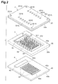
Fig. 2 is an exploded perspective view of the photomultiplier shown inFig. 1 ; -
Fig. 3 is a plan view of a sidewall frame shown inFig. 1 ; -
Fig. 4 is a partly broken perspective view showing major parts of the sidewall frame and lower frame shown inFig. 1 (including a section along the line II-II of the photomultiplier shown inFig. 1 ); -
Fig. 5 is a sectional view along the line V-V of the photomultiplier shown inFig. 1 ; -
Fig. 6 is a partly broken perspective view of the sidewall frame and lower frame shown inFig. 1 , particularly, in a region near the electron multiplier; -
Fig. 7 shows drawings for explaining structures of the electron multiplier shown inFig. 6 and its constituent elements, wherein (A) is a partly broken view of the electron multiplier shown inFig. 6 , (B) is a perspective view showing the shape of a column, and (C) is a perspective view showing the shape of a column surface; -
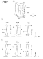
Fig. 8 shows drawings for explaining the structure of columns: wherein- (A) is a partly broken view of a column along the line I-I in
Fig. 7(B) , - (B) is a drawing showing variations where the sectional shape in (A) is realized by curves, and (C) is a drawing showing variations where the sectional shape in (A) is realized by straight lines;
- (A) is a partly broken view of a column along the line I-I in
-
Fig. 9 shows drawings for explaining a processing simulation of the column surface where a secondary electron emitting surface is formed; -
Fig. 10 is a section along the line II-II of the photomultiplier shown inFig. 1 , and a drawing for explaining a specific installation state of an example of dynodes (columns on each of which the secondary electron emitting surface is formed) forming a part of the electron multiplier; -
Fig. 11 shows are drawings showing structures of other examples of the dynodes (columns on each of which the secondary electron emitting surface is formed) installed in the photomultiplier as inFig. 10 (corresponding to the section along the line II-II of the photomultiplier shown inFig. 1 ), wherein (A) is a drawing showing a sectional shape of a conventional dynode, (B) is a drawing showing a sectional shape of a dynode according to a first modification example, and (C) is a drawing showing a sectional shape of a dynode according to a second modification example; -
Fig. 12 shows drawings for explaining effects of the embodiment of the present invention (corresponding to the section along the line II-II of the photomultiplier shown inFig. 1 ), wherein (A) is a drawing showing a conventional structure and (B) is a drawing showing the structure of the embodiment; -
Fig. 13 is a drawing showing a sectional shape of dynodes according to a third modification example, along with a specific installation state, and drawing for explaining the effect of the dynodes according to the third modification example (corresponding to the section along the line II-II of the photomultiplier shown inFig. 1 ); -
Fig. 14 shows drawings showing structures of respective portions in the photomultiplier shown inFig. 1 , wherein (A) is a bottom view from the back side of the upper frame shown inFig. 1 and (B) is a plan view of the sidewall frame shown inFig. 1 ; -
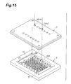
Fig. 15 is a perspective view showing a connection state of the upper frame and the sidewall frame shown inFig. 14 ; -
Fig. 16 shows partly broken perspective views of the sidewall frame and lower frame shown inFig. 1 (corresponding to the section along the line II-II of the photomultiplier shown inFig. 1 ), wherein (A) is a drawing in which the lower frame of a first structure is applied and (B) is a drawing in which the lower frame of a second structure example is applied; -
Fig. 17 is a plan view of the electron multiplier according to a first comparative example; -
Fig. 18 is a plan view of the electron multiplier according to a second comparative example; -
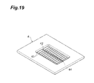
Fig. 19 is a perspective view of the lower frame in the photomultiplier according to a first modification example of the present invention; -
Fig. 20 is a bottom view from the back side of the lower frame shown inFig. 19 ; and -
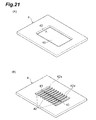
Fig. 21 shows perspective views of the lower frame in the photomultiplier according to a second modification example of the present invention, wherein (A) is a drawing showing a third structure of the lower frame applicable to the photomultiplier of the second modification example and (B) is a drawing showing a fourth structure of the lower frame applicable to the photomultiplier of the second modification example. - Each of embodiments of the dynodes, electron multiplier, and photomultiplier according to the present invention will be described below in detail with reference to the accompanying drawings. In the description of drawings identical or equivalent portions will be denoted by the same reference signs, without redundant description.
-
Fig. 1 is a perspective view showing a configuration of an embodiment of the photomultiplier according to the present invention andFig. 2 an exploded perspective view of thephotomultiplier 1 shown inFig. 1 . - The
photomultiplier 1 shown inFig. 1 is a photomultiplier tube with a transmissive photocathode and is provided with ahousing 5 as an envelope composed of an upper frame (second substrate) 2, asidewall frame 3, and a lower frame (first substrate) 4 opposed to theupper frame 2 with thesidewall frame 3 in between. Thisphotomultiplier 1 is an electron tube in which a direction of incidence of light to the photocathode intersects with a direction of multiplication of electrons in an electron multiplier. Namely, thephotomultiplier 1 is an electron tube in which when light is incident from a direction intersecting with a plane made by thelower frame 4, which is indicated by arrow A inFig. 1 , photoelectrons emitted from the photocathode move into the electron multiplier, cascade multiplication of secondary electrons is induced in a direction intersecting with the direction indicated by arrow A, which is indicated by arrow B, and a signal is taken out from an anode. - In the description hereinafter, an upstream side (photocathode side) of electron multiplication paths (electron multiplication channels) along the electron multiplication direction will be referred to as "first end side" and a downstream side (anode side) thereof as "second end side." Each of the constituent elements of the
photomultiplier 1 will be described below in detail. - As shown in
Fig. 2 , theupper frame 2 is comprised of a base material ofwiring substrate 20 whose major material is an insulating ceramic of a rectangular flat plate shape. An example of such a wiring substrate to be used is a multilayer wiring substrate using LTCC (Low Temperature Co-fired Ceramics) or the like allowing fine wiring design and free design of wiring patterns on the front and back. Thewiring substrate 20 has a plurality ofconductive terminals 201A-201D on itsprincipal surface 20b, which are electrically connected to thesidewall frame 3, below-describedphotocathode 41, focusingelectrode 31,wall electrode 32,electron multiplier 33, andanode 34 so as to implement power feeding from the outside and extraction of signal. Theconductive terminals 201 A are provided for power feeding to thesidewall frame 3; theconductive terminals 201B are provided for power feeding to thephotocathode 41, focusingelectrode 31, andwall electrode 32; theconductive terminals 201C are provided for power feeding to theelectron multiplier 33; theconductive terminals 201D are provided for power feeding to theanode 34 and extraction of signal. Theseconductive terminals 201A-201D are connected respectively to conductive films and conductive terminals (the details of which will be described below) on an insulatingopposite surface 20a opposite to theprincipal surface 20b in thewiring substrate 20, and these conductive films and conductive terminals are connected to thesidewall frame 3,photocathode 41, focusingelectrode 31,wall electrode 32,electron multiplier 33, andanode 34. Theupper frame 2 does not always have to be limited to the multilayer wiring substrate provided with the conductive terminals 201, but it may be a platelike member of an insulating material such as a glass substrate, through which the conductive terminals for power feeding from the outside and extraction of signal are provided. - The
sidewall frame 3 is comprised of a base material of asilicon substrate 30 of a rectangular flat plate shape. A penetratingpart 301 surrounded by a frame-like sidewall part 302 is formed from aprincipal surface 30a of thesilicon substrate 30 toward asurface 30b opposed thereto. This penetratingpart 301 is formed so as to have a rectangular aperture and the periphery thereof along the periphery of thesilicon substrate 30. - In this
penetrating part 301, there are thewall electrode 32, focusingelectrode 31,electron multiplier 33, andanode 34 arranged from the first end side toward the second end side. Thesewall electrode 32, focusingelectrode 31,electron multiplier 33, andanode 34 are formed by processing thesilicon substrate 30 by RIE (Reactive Ion Etching) processing or the like, and a major material thereof is silicon. - The
wall electrode 32 is an electrode of a frame shape formed so as to surround the below-describedphotocathode 41, when viewed from a direction normal to anopposite surface 40a of below-described glass substrate 40 (which is a direction approximately perpendicular to theopposite surface 40a). The focusingelectrode 31 is an electrode that focuses photoelectrons emitted from thephotocathode 41 and guides them to theelectron multiplier 33, and is disposed between thephotocathode 41 and theelectron multiplier 33. - The
electron multiplier 33 is composed of N stages (N is an integer of 2 or more) of dynodes (electron multiplying portions) set at different potentials along the electron multiplication direction from thephotocathode 41 to the anode 34 (which is the direction indicated by arrow B inFig. 1 and which will be the same hereinafter), and has a plurality of electron multiplication paths (electron multiplication channels) extending across each of the stages in the electron multiplication direction. Theanode 34 is located at a position where theelectron multiplier 33 is sandwiched between theanode 34 and thephotocathode 41. - Each of these
wall electrode 32, focusingelectrode 31,electron multiplier 33, andanode 34 is fixed to thelower frame 4 by anodic bonding, diffusion bonding, or bonding with a seal material such as a low-melting-point metal (e.g., indium), whereby they are two-dimensionally arranged on thelower frame 4. - The
lower frame 4 is comprised of a base material ofglass substrate 40 of a rectangular flat plate shape. Thisglass substrate 40 forms theopposite surface 40a of glass as an insulating material that is opposed to theopposite surface 20a of thewiring substrate 20 and that is an internal surface of thehousing 5. Thephotocathode 41 of a transmissive photoelectric surface is formed in a portion opposite to thepenetrating part 301 of the sidewall frame 3 (which is a portion except for a bonding region to the sidewall part 302) and at an end on the side opposite to theanode 34 side, on theopposite surface 40a. A plurality ofrecesses 42 of a rectangular shape are formed in a portion where theelectron multiplier 33 andanode 34 are mounted on theopposite surface 40a, in order to prevent multiplied electrons from entering theopposite surface 40a. The multistage dynodes constituting theelectron multiplier 33, and theanode 34 are arranged onintermediate portions 42a which are flat portions between therecesses 42. - Next, the internal structure of the
photomultiplier 1 will be described in detail with reference toFigs. 3 to 5 .Fig. 3 is a plan view of thesidewall frame 3 shown inFig. 1 ,Fig. 4 a partly broken perspective view showing the major parts of thesidewall frame 3 andlower frame 4 shown inFig. 1 (including a section along the line II-II of the photomultiplier inFig. 1 ), andFig. 5 a sectional view along the line V-V of the photomultiplier shown inFig. 1 . - As shown in
Fig. 3 , theelectron multiplier 33 in thepenetrating part 301 is composed ofmultistage dynodes 33a-331 arranged in order as spaced apart, from the first end side to the second end side on theopposite surface 40a (in the direction indicated by arrow B, which is the electron multiplication direction). Thesemultistage dynodes 33a-331 form a plurality of parallel electron multiplication channels C each consisting of N electron multiplication holes provided in series from the first-stage dynode 33a on the first end side to the last-stage (Nth)dynode 331 on the second end side along the direction indicated by arrow B. Therecesses 42 are provided between the focusingelectrode 31 and the first-stage dynode 33a, between each pair of adjacent two of themultistage dynodes 33a-331, and between the last-stage dynode 331 and theanode 34, and themultistage dynodes 33a-331 are arranged on the respectiveintermediate portions 42a being the flat portions located between therecesses 42 provided in thelower frame 2 inFig. 2 . - The
photocathode 41 is provided with a space from the first-stage dynode 33a on the first end side and located on the first end side on theopposite surface 40a with the focusingelectrode 31 in between. Thisphotocathode 41 is formed as a transmissive photoelectric surface of a rectangular shape on theopposite surface 40a of theglass substrate 40. When incident light from the outside passing through theglass substrate 40 of thelower frame 4 reaches thephotocathode 41, it emits photoelectrons according to the incident light and the photoelectrons are guided to the first-stage dynode 33a by thewall electrode 32 and the focusingelectrode 31. - The
anode 34 is provided with a space from the last-stage dynode 331 on the second end side and located on the second end side on theopposite surface 40a. Thisanode 34 is an electrode for extracting electrons resulting from the multiplication in the direction indicated by arrow B in the electron multiplication channels C by theelectron multiplier 33, as an electric signal to the outside, and has a plurality of depressions corresponding to the respective electron multiplication channels C. Each depression, when viewed from a direction perpendicular to theopposite surface 40a of thelower frame 4, is of a saclike shape open on one sidewall face side facing theelectron multiplier 33 and closed on the other sidewall face side, and is provided with a projecting portion to narrow an entrance space, at an entrance of the depression on the one sidewall face side. Namely, theanode 34 is shaped so as to confine the multiplied electrons entering the depressions, whereby theanode 34 can extract the multiplied electrons as a signal with greater certainty. There is also therecess 42 between theanode 34 and thesidewall part 302 opposed to a second-end side face of theanode 34, and theanode 34 is arranged on theintermediate portion 42a being the flat portion located betweenrecesses 42. - As shown in
Fig. 4 , each of themultistage dynodes 33a-33d is arranged on theintermediate portion 42a of the flat portion located betweenrecesses 42 formed on theopposite surface 40a of thelower frame 4 and is separated from bottoms of the respective recesses 42. Thedynode 33a includes a plurality ofcolumns 51a arranged in a direction approximately perpendicular to the electron multiplication direction and along theopposite surface 40a and extending nearly perpendicularly toward theopposite surface 20a of theupper frame 2, and a pedestal (support) 52a (330) continuously formed at ends on therecess 42 side of thecolumns 51a (51) and extending in a direction approximately perpendicular to the electron multiplication direction and along the bottoms of therecesses 42. Furthermore, thedynodes 33b-33d also have the same structure as thedynode 33a, as to thecolumns 51b-51d andpedestal 52b-52d, respectively. The electron multiplication channels C are formed between adjacent members in therespective columns 51a-51d and thepedestals 52a-52d are disposed across a region Ac (Fig. 3 ) where the electron multiplication channels C are formed. Thepedestals 52a-52d function each to electrically connect the plurality ofcolumns 51a-51d, respectively, and to keep the plurality ofcolumns 51a-51d separate from the bottoms of therecesses 42. In the present embodiment, each of thedynodes 33a-33d is configured so that thecolumns 51a-51d and thepedestal 52a-52d are integrally formed, but the columns and pedestal may be separately formed. Secondary electron emitting surfaces are formed in predetermined regions of therespective columns 51a-51d and sectional shapes of thesecolumns 51a-51d are designed to minimize the width near an x-y plane P located approximately in the middle between thelower frame 4 and the upper frame 2 (or on the side nearer to the lower frame 4), as shown inFig. 4 . Although not shown, thedynodes 33e-331 also have the same structure. - Furthermore, at one end in the direction perpendicular to the electron multiplication direction in each of the
pedestals power feeding portion pedestal upper frame 2. Thepower feeding portions columns pedestals - As shown in
Fig. 5 , thedynode 33b is secured to thelower frame 4 in such a manner that a lower surface of thepedestal 52b extending in the direction perpendicular to the electron multiplication direction and along theopposite surface 40a is bonded to theintermediate portion 42a of the flat portion of theopposite surface 40a. Although there are some differences in detailed shape, theother dynodes recesses 42 on theopposite surface 40a are formed in a width slightly larger than the arrangement spacing of the pedestals of themultistage dynodes 33a-331 and theanode 34. Namely, therecesses 42 are intermittently formed via theintermediate portions 42a of flat portions in theopposite surface 40a of thelower frame 4, so as to increase creeping distances between the pedestals of thedynodes 33a-331 and theanode 34. The secondary electron emitting surfaces are formed in thecolumns 51b and the sectional shape of thesecolumns 51b is designed to minimize the width near the x-y plane P located approximately in the middle between thelower frame 4 and theupper frame 2, as shown inFig. 5 . - The shape of the columns forming each of the
multistage dynodes 33a-331, particularly, the shape of the secondary electron emitting surfaces will be described below in detail. -
Fig. 6 is a partly broken perspective view of the sidewall frame and lower frame shown inFig. 1 , particularly, in a region near the electron multiplier.Fig. 7 shows drawings for explaining the structure of the electron multiplier and constituent elements thereof shown inFig. 6 , whereinFig. 7(A) is a partly broken view of the electron multiplier inFig. 6 ,Fig. 7(B) a perspective view showing the shape of the column at a location indicated by S inFig. 7(A), and Fig. 7(C) a perspective view showing the shape of the surface of the column.Fig. 8 shows drawings for explaining the structure of the column, whereinFig. 8(A) is a partly broken view of the column along the line I-I inFig. 7(B) ,Fig. 8(B) a drawing showing variations where the sectional shape inFig. 8(A) is realized by curves, andFig. 8(C) a drawing showing variations where the sectional shape inFig. 8(A) is realized by straight lines.Fig. 9 shows drawings for explaining a processing simulation of the surface of the column on which the secondary electron emitting surface is formed, whereinFig. 9(A) shows a processing region of the column,Fig. 9(B) shows a minimum processing element inFig. 9(A), and Fig. 9(C) is a drawing showing a progress of a processing process with the lapse of time. -
Fig. 6 shows the structure near theelectron multiplier 33 so that the x-axis in the drawing is included in the section along the line II-II inFig. 1 . Namely, the plurality ofrecesses 42 are provided on theopposite surface 40a of the lower frame 40 (glass substrate) and themultistage dynodes 33a-331 are arranged on the respectiveintermediate portions 42a located between theserecesses 42. The side faces of the respective pedestals of themultistage dynodes 33a-331 are processed in a curved shape or a tapered shape. The conductive films 202 (evaporated electrodes for countermeasures against hysteresis) provided on theopposite surface 20a of theupper frame 2 are connected to the respectiveconductive terminals 201C and a conductive material 205 (described below) electrically connects theconductive film 202 to thepower feeding portion 53a-531 of each of themultistage dynodes 33a-331. - As shown in
Fig. 7(A) , the side faces of thepedestals 330 of themultistage dynodes 33a-331 are processed in a tapered shape to become thinner in the direction from theupper frame 2 to thelower frame 4. When the side faces are processed in this manner, the distance between adjacent dynodes is increased. Furthermore, therecess 42 is provided between adjacent dynodes, thereby to further increase the creeping distance between adjacent dynodes, which is defined on theopposite surface 40a of thelower frame 4. The region where the secondaryelectron emitting surface 520 of eachcolumn 51 is formed has, as shown inFig. 7(B) , such a shape that normal vectors to respective portions of the secondaryelectron emitting surface 520 are directed to an intermediate point of the column 51 (position intersecting with the x-y plane P inFig. 5 ). The directions of the normal vectors shown inFig. 7(B) are directions of emission of secondary electrons with the highest emission probability. In the present embodiment example, the height of the column 51 (length along the direction from thelower frame 4 to the upper frame 2) is 800 µm, and the region where the secondary electron emitting surface of thiscolumn 51 is formed has a constricted structure in which the intermediate position along the height direction of the column 51 (the position intersecting with the x-y plane P inFig. 5 ) is located 50 µm inward into the interior of thecolumn 51. - Namely, as shown in
Figs. 6 and7 , each of the columns 51 (corresponding to 51a-511) forming the respective stages ofdynodes 33a-33d is processed so that the section thereof perpendicular to theopposite surface 40a of the lower frame 4 (which will be referred to hereinafter as vertical section and which corresponds to the x-z plane), specifically, the shape of the region R where the secondaryelectron emitting surface 520 is formed, is depressed in a curved or tapered shape along the z-axis direction (cf.Figs. 6 and7(A) ). For example, as shown inFigs. 7(B) and 7(C) , the height of each column (in the z-axis direction) is 800 µm, and the shape of the region where the secondary electron emitting surface is formed is processed to the constricted shape depressed by 50 µm from each end (the end located on thelower frame 4 side and the end located on theupper frame 2 side), at the intermediate point (position intersecting with the x-y plane P inFig. 5 ). -
Fig. 8(A) shows an example of the vertical section (x-z plane) of eachcolumn 51. It is noted that the section 510 (hatched portion) of thecolumn 51 in thisFig. 8(A) is the vertical section along the line I-I inFig. 7(B) . For processing of this vertical section, for example, the secondaryelectron emitting surface 520 may be processed as defined by curves, as shown inFig. 8(B) , or the secondaryelectron emitting surface 520 may be processed as defined by straight lines, as shown inFig. 8(C) . - Namely, in the
photomultiplier 1 of the present embodiment, as shown inFigs. 8(A) to 8(C) , each of themultistage dynodes 33a-331 is formed so that the region where the secondary electron emitting surface is formed has the constricted structure. More specifically, in the section (x-z plane) along the line II-II inFig. 1 , the region R where the secondaryelectron emitting surface 520 is formed has the shape to minimize the width in the x-axis direction (direction indicated by arrow B), for example, at a certain position Q of the column 51 (the same also applies to the other columns). In the section (x-z plane) along the line II-II inFig. 1 , the region R where the secondaryelectron emitting surface 520 is formed has one or more constricted shapes. Each constricted shape is such a shape that the width in the x-axis direction decreases monotonically and then increases monotonically in the direction from thelower frame 4 to theupper frame 2. Furthermore, for example, the secondary electron emitting surface of thedynode 33a has the section (x-z plane) along the line II-II inFig. 1 , which is defined by line segments including one or more depressed shapes entering into thecolumn 51. When the sectional shape of thecolumn 51 is viewed along the x-y plane, an area or a peripheral length of the section becomes minimum at the position Q in the region R where the secondaryelectron emitting surface 520 is formed. - In
Figs. 8(B) and 8(C) , the position Q of "constriction" (which is the portion with the minimum width along the x-axis direction of the section) in each of thesections electron emitting surface 520 is formed. The position Q of "constriction" (portion with the minimum width along the x-axis direction of the section) in each of thesections upper frame 2 than the intermediate point) in the region R where the secondaryelectron emitting surface 520 is formed. The position Q of "constriction" (region with the minimum width along the x-axis direction of the section) in each of thesections lower frame 4 than the intermediate point) in the region R where the secondaryelectron emitting surface 520 is formed. - In any one of the variations, the portion Q with the smallest width of the
vertical section 510 of eachcolumn 51 is present in the region R where the secondary electron emitting surface is formed. In the region R, a vertical section of each column along the y-axis direction (corresponding to the y-z plane) also decreases monotonically and then increases monotonically from the portion indicated by Q in the drawing, along the height direction of each column (z-axis direction) extending from thelower frame 4 to the upper frame. - The
columns 51 with the vertical section as described above can be formed, for example, by etching as shown inFig. 9. Fig. 9(A) shows a part of the column 51 (a region indicated by region AR inFig. 9(A) ) having thevertical section 510d. The secondaryelectron emitting surface 520 is formed in the etched region.Fig. 9(C) is a drawing showing the result of a processing simulation, in which a progress of etching is shown with the lapse of time. Each ofsections 900A-900R inFig. 9(C) is composed of minimum processing elements shown inFig. 9(B) . As understood from the minimum processing elements shown in thisFig. 9(B) , the etched surface is curved. Furthermore, numeral 910 represents an etching mask in each of thesections 900A-900R inFig. 9(C) . In addition, numeral 920 represents an internal protecting film to be filled so as to function as an etching mask, in a region being etched along an intendedline 521 of etching. - Next, specific installation states of the
columns 51 which can be realized by the various sectional shapes as described above will be described below with reference toFigs. 10 and11(A)-11(C) .Fig. 10 is a section along the line II-II of thephotomultiplier 1 inFig. 1 and a drawing for explaining a specific installation state of an example ofdynodes 33a-331 (columns 51 where the secondary electron emitting surfaces are formed) forming a part of theelectron multiplier 33.Fig. 11 shows drawings (corresponding to the section along the line II-II of thephotomultiplier 1 inFig. 1 ) showing structures of other examples of thedynodes 33a-331 (columns 51 where the secondary electron emitting surfaces are formed) installed in thephotomultiplier 1 as inFig. 10 , whereinFig. 11(A) is a drawing showing a sectional shape of a conventional dynode,Fig. 11(B) a drawing showing a sectional shape of a dynode according to a first modification example, andFig. 11(C) a drawing showing a sectional shape of a dynode according to a second modification example. It is assumed in the examples ofFigs. 10 and11(A)-11(C) that theupper frame 2 is comprised of aglass substrate 20. - As shown in
Fig. 10 , theglass substrate 40 of thelower frame 4 is provided with a plurality ofrecesses 42 on itsopposite surface 40a and the pedestals 330 (with the thickness of 200 µm) of the respective stages of dynodes are installed on the respectiveintermediate portions 42a located between theserecesses 42. On eachpedestal 330 thecolumns 51 with the secondary electron emitting surface being formed on the side face thereof are installed integrally with thepedestal 330. Theseintegrated pedestal 330 andcolumns 51 constitute each stage of dynode. On the other hand, in theglass substrate 20 of theupper frame 2, theconductive terminals 201C are in contact with the respectiveconductive films 202 evaporated on theopposite surface 20a of theglass substrate 20, and eachconductive film 202 is electrically connected through theconductive material 205 to the top part of each column 51 (in practice, to thepower feeding portion 53a-531 of each stage of dynode). In this structure, theglass substrate 20 and the top part of eachcolumn 51 are separated by 50 µm. - The shape of the region R where the secondary
electron emitting surface 520 of eachcolumn 51 shown inFig. 10 is formed has a constricted structure (shape entering into thecolumn 51 by L) at a position nearer to thelower frame 2 than the intermediate position of the region R. Namely, a region A above the position of constriction is wider than a region B below the position of constriction. Specifically, the length in the height direction of the region R where the secondaryelectron emitting surface 520 is formed is 800 µm, and a ratio (A:B) of the length in the height direction of the region A to the length in the height direction of the region B can be in the range of 1:1 to 10: 1 and, preferably, in the range of 3:2 to 7:1. The depth C to define the constricted structure can be in the range of 20 µm to 150 µm and, preferably, in the range of 30 µm to 80 µm. -
Fig. 11(A) shows an installation state of a dynode to which the conventional sectional shape is applied, which is the same as the installation state shown inFig. 10 , except for the sectional shape of thecolumn 51.Fig. 11(B) shows an installation state of a dynode according to the first modification example, which is different in the sectional shape of thepedestal 330 and the sectional shape of thecolumn 51, from the structure shown inFig. 10 . Namely, in the example shown inFig. 11(B) , the side face of thepedestal 330 is processed in a tapered shape. The position of constriction in thecolumn 51 is located near the intermediate point of the region R where the secondaryelectron emitting surface 520 is formed (a maximum point where emitted secondary electrons are concentrated is also located near the intermediate point). The example shown inFig. 11(C) is different from the structure shown inFig. 10 , in that the side face of thepedestal 330 is processed in a tapered shape. Furthermore, in the installation state ofFig. 11(C) , the position of constriction in thecolumn 51 is located on the lower side (glass substrate 40 side) with respect to the intermediate point of the region R where the secondaryelectron emitting surface 520 is formed, and, naturally, a maximum point where emitted secondary electrons are concentrated is also located on the lower side with respect to the intermediate point. - When the length of the secondary
electron emitting surface 520 in the height direction of thecolumn 51 is defined as 2a inFig. 11 (A) , the length of the secondaryelectron emitting surface 520 inFig. 11(B) is 2.83a and the length of the secondaryelectron emitting surface 520 inFig. 11(C) is 2.92a. When the structure shown inFig. 11(C) is employed in this manner, it offers an effect of increase in the area of the secondaryelectron emitting surface 520 itself. It also has an effect of suppressing occurrence of black silicon (needlelike foreign matter) during manufacture. Furthermore, since the maximum point where emitted secondary electrons are concentrated can be located away from the glass substrate (particularly, from theglass substrate 20 of the upper frame 2), it is feasible to suppress unwanted luminescence and, particularly, to prevent noise which can be produced by the luminescence passing through the separate space between theglass substrate 20 and the tops of thecolumns 51 to reach thephotocathode 41. It is also feasible to suppress reduction in withstand voltage characteristic between theconductive films 202 due to incidence of secondary electrons into theglass substrate 20 of theupper frame 2. In addition, since the creeping distance between adjacent dynodes can be increased by the degree of the length D illustrated in thepedestal 330 inFig. 11(B) , in the examples ofFigs. 11(B) and 11(C) , it is feasible to achieve drastic improvement in withstand voltage characteristic. - The effects of the
columns 51 processed as described above will be described below usingFig. 12. Fig. 12 shows drawings for explaining the effects of the present embodiment (corresponding to the section along the line II-II of the photomultiplier inFig. 1 ), whereinFig. 12(A) shows the conventional structure andFig. 12(B) is a drawing showing the structure of the present embodiment. The left side ofFig. 12(A) and the left side ofFig. 12(B) show some of the respective stages of dynodes forming the central part of theelectron multiplier 33. On the other hand, the right side ofFig. 12(A) and the right side ofFig. 12(B) show some of the respective stages of dynodes forming the rear stage side of theelectron multiplier 33 including theanode 34. - In the case of the conventional structure shown in
Fig. 12(A) (in which the width of the vertical section of thecolumns 51 is constant along the height direction), thepedestals 330 of the respective stages of dynodes are installed on theglass substrate 40 of thelower frame 4. Thecolumns 51 with the secondary electron emitting surface being formed on the side face thereof, are installed on thepedestals 330, integrally with thepedestals 330. Theseintegrated pedestal 330 andcolumns 51 constitute each stage of dynode. On the other hand, in theglass substrate 20 of theupper frame 2, theconductive terminals 201 C are in contact with the respectiveconductive films 202 evaporated on theopposite surface 20a of theglass substrate 20 and eachconductive film 202 is electrically connected through theconductive material 205 to the top part of each column 51 (in practice, to thepower feeding portion 53a-531 of each stage of dynode). Theanode 34 is also composed of the pedestal and columns and extracts the arriving secondary electrons as a signal through theconductive terminal 201D. - In the example of
Fig. 12(A) , the secondary electron emitting surfaces 520 (electrodes) are perpendicular to the glass substrate 40 (lower frame 4). In this case, many secondary electrons collide with the surfaces of the insulating support substrate (lower frame 4) and the penetrating electrode substrate (upper frame 2), i.e., with the surfaces of glass being an insulating material, so as to produce unwanted luminescence. This luminescence becomes a noise source and, in light sensors employing the conventional structure, it is a cause to decrease S/N thereof. Since secondary electrons colliding with the glass surfaces make no contribution to electron multiplication, they decrease the electron multiplication rate (gain characteristic) and also degrade the withstand voltage characteristic between electrodes. - On the other hand, in the case of the structure of the present embodiment shown in
Fig. 12(B) (where the width of the vertical section of each columm is made thinner near the center along the height direction), theglass substrate 40 of thelower frame 4 is provided with therecesses 42 on theopposite surface 40a thereof and thepedestals 330 of the respective stages of dynodes are installed on theintermediate portions 42a of the flat portions located between theserecesses 42. Thecolumns 51 with the secondary electron emitting surface of the curved shape being formed on the side face thereof are installed on eachpedestal 330, integrally with thepedestal 330. Theseintegrated pedestal 330 andcolumns 51 constitute each stage of dynode. On the other hand, in theglass substrate 20 of theupper frame 2, theconductive terminals 201C are in contact with the respectiveconductive films 202 evaporated on theopposite surface 20a of theglass substrate 20 and eachconductive film 202 is electrically connected through theconductive material 205 to the top part of each column 51 (in practice, to thepower feeding portion 53a-531 of each stage of dynode). Theanode 34 is also composed of the pedestal and columns, and extracts the arriving secondary electrons as a signal through theconductive terminal 201D. The pedestal of theanode 34 is also installed on theintermediate portion 42a being the flat portion betweenrecesses 42. - In the example of
Fig. 12(B) , the secondary electron emitting surfaces (electrodes) are curved toward the centers thereof. Namely, in this shape, the spacing between adjacent dynodes is narrower on the end sides than in the region near the centers of the secondary electron emitting surfaces. This configuration drastically reduces the number of secondary electrons colliding with the surfaces of the glass substrate 40 (lower frame 4) and the glass substrate 20 (upper frame 2), i.e., with the surfaces of glass being the insulating material and, as a result thereof, the unwanted luminescence is effectively suppressed. Therefore, a light sensor employing the structure of the present embodiment is improved in S/N thereof and thus can perform highly accurate detection of light, as an effect of the suppression of luminescence. Since the secondaryelectron emitting surface 520 itself has the curved shape, the effective area of the secondaryelectron emitting surface 520 becomes larger without change in height of eachcolumn 51. For this reason, the electron multiplication rate can be drastically improved by synergistic effect of the increase in electron multiplication rate by the decrease of secondary electrons causing luminescence, and the expansion of the effective area. - Furthermore, a specific installation state of
columns 51 that can be realized by another sectional shape of dynodes will be described below with reference toFig. 13. Fig. 13 is a drawing showing the sectional shape of dynodes according to a third modification example, together with the specific installation state thereof, and drawing for explaining the effect of the dynodes according to the third modification example (which corresponds to the section along the line II-II of the photomultiplier inFig. 1 ). It is also assumed that theupper frame 2 is comprised of aglass substrate 20 in the structure ofFig. 13 . - As shown in
Fig. 13 , theglass substrate 40 of thelower frame 4 is provided with a plurality ofrecesses 42 on itsopposite surface 40a and the pedestals 330 (with the thickness of 200 µm) of the respective stages of dynodes are installed on theintermediate portions 42a being flat portions located between theserecesses 42. Thecolumns 51 with the secondary electron emitting surface being formed on the side face thereof are installed on eachpedestal 330, integrally with thepedestal 330. Theseintegrated pedestal 330 andcolumns 51 constitute each stage of dynode. On the other hand, in theglass substrate 20 of theupper frame 2, theconductive terminals 201C are in contact with the respectiveconductive films 202 evaporated on theopposite surface 20a of theglass substrate 20 and eachconductive film 202 is electrically connected through theconductive material 205 to the top of each column 51 (in practice, to thepower feeding portion 53a-531 of each stage of dynode). In this structure, theglass substrate 20 and the tops of thecolumns 51 are spaced apart by 50 µm. - Particularly, the shape of the region where the secondary
electron emitting surface 520 of eachcolumn 51 shown inFig. 13 is formed is different in possession of two constricted structures (which may be three or more constricted structures), from the aforementioned structures shown inFigs. 10 ,11(B), and 11(C) . Namely, in the example ofFig. 13 , a curved surface with greater curvature is formed in the part nearer to the glass substrate 20 (region R2), whereby secondary electrons emitted therefrom are guided away from the glass substrate 20 (i.e., the secondary electrons generated in the region R2 are guided to region R1). This configuration decreases the number of secondary electrons colliding with theglass substrate 20 of theupper frame 2 and thus can effectively reduce the noise due to luminescence and withstand voltage failure due to electrification. - A wiring structure of the
photomultiplier 1 will be described below with reference toFigs. 14 and15 .Fig. 14(A) is a bottom view from theback surface 20a side of theupper frame 2, andFig. 14(B) a plan view of thesidewall frame 3.Fig. 15 is a perspective view showing a connection state between theupper frame 2 and thesidewall frame 3. - As shown in
Fig. 14(A) , theopposite surface 20a of the upper frame 2 (which may be comprised of an insulating material such as glass) is provided with a plurality of conductive films (power feeding portions) 202 electrically connected respectively to theconductive terminals upper frame 2, andconductive terminals 203 electrically connected to the respectiveconductive terminals 201A inside theupper frame 2. In theelectron multiplier 33, as shown inFig. 14(B) ,power feeding portions 53a-531 for connection to the correspondingconductive films 202 are provided in an upright state, as described previously, and apower feeding portion 37 for connection to theconductive film 202 is provided in an upright state at an end of theanode 34. Furthermore, apower feeding portion 38 for connection to theconductive film 202 is provided in an upright state at a corner of thewall electrode 32. The focusingelectrode 31 is formed integrally with thewall electrode 32 on thelower frame 4 side so as to be electrically connected to thewall electrode 32. Furthermore, aconnection 39 of a rectangular flat plate shape is formed integrally with thewall electrode 32 on theopposite surface 40a side of thelower frame 4 and thisconnection 39 is bonded to a conductive film (not shown) formed in electrical contact with thephotocathode 41 on theopposite surface 40a, thereby achieving electrical connection between thewall electrode 32 and thephotocathode 41. - As shown in
Fig. 15 , when theupper frame 2 and thesidewall frame 3 of the above configuration are bonded to each other, theconductive terminals 203 come to be electrically connected to thesidewall part 302 of thesidewall frame 3. In addition, thepower feeding portions 53a-531 of theelectron multiplier 33, thepower feeding portion 37 of theanode 34, and thepower feeding portion 38 of thewall electrode 32 are independently connected each through a conductive member of gold (Au) or the like to the correspondingconductive films 202. In this connection configuration, thesidewall part 302, theelectron multiplier 33, and theanode 34 are electrically connected to theconductive terminals wall electrode 32, together with the focusingelectrode 31 and thephotocathode 41, is electrically connected to the conductive terminal 201B to realize power feeding from the outside (cf.Fig. 15 ). - As shown in
Fig. 14(B) , the shape of thepedestal 52b andpower feeding portion 53b of thedynode 33b is so defined that the sectional area S1 along theopposite surface 40a of one end continuous to thepower feeding portion 53b out of the two ends of thepedestal 52b of thedynode 33b becomes larger than the sectional area S2 along theopposite surface 40a of the other end out of the two ends. This size relation between the one end with thepower feeding portion 53b and the other end in thedynode 33b is continuously satisfied throughout the entire ends of thedynode 33b, i.e., up to the surface on theupper frame 2 side. For this reason, the one end with thepower feeding portion 53b is larger than the other end in terms of the area, when viewed from the direction normal to theopposite surface 40a, and in terms of the volume thereof as well. In this manner, the one end with thepower feeding portion 53b is superior in physical strength and, in addition thereto, the surface on theupper frame 2 side is large enough to increase the contact area with the conductive member of gold (Au) or the like, which is also effective to secure electrical connection. Theother dynodes electron multiplier 33 are also defined in the sectional shape satisfying the same relation. Themultistage dynodes 33a-331 are arranged so that their one ends on the side of thepower feeding portions 53a-531 and the other ends on the opposite side are aligned in a staggered manner along the electron multiplication direction on theopposite surface 40a. In other words, themultistage dynodes 33a-331 are disposed on theopposite surface 40a so that the orientations of the pedestals based on the arrangement direction of thepower feeding portions 53a-531 thereof (orientations of the pedestals defined in the direction extending from the one end with the power feeding portion to the other end) are alternately opposite to each other. - In the
photomultiplier 1 described above, incident light is incident into thephotocathode 41 to be converted to photoelectrons, the photoelectrons are incident into the electron multiplication channels C formed by themultistage dynodes 33a-331 on theinner surface 40a of thelower frame 4 in thehousing 5 to be multiplied, and the multiplied electrons are extracted as an electric signal from theanode 34. - Explaining the example of the
dynodes 33a-33d, eachdynode 33a-33d is provided with thepedestal 52a-52d at the end on thelower frame 4 side, thepower feeding portion 53a-53d extending from the one end toward theupper frame 2 opposed to thelower frame 4 is electrically connected to thepedestal 52a-52d, and thepower feeding portion 53a-53d is connected to theconductive film 202 provided on theinner surface 20a of theupper frame 2, thereby implementing power feeding to eachdynode 33a-33d. Furthermore, therecesses 42 as shown inFig. 2 are formed in the region enclosed in a dashed line, on theopposite surface 40a of thelower frame 4, and thepedestal 52a-52d is installed on theintermediate portion 42a being the flat portion located betweenrecesses 42. The sectional area S1 along theopposite surface 40a of the one end on thepower feeding portion 53a-53d side is larger than the sectional area S2 of the other end. As the strength is increased at the end of thepedestal 52a-52d on the side in contact with theconductive film 202 of theupper frame 2, the physical strength of theelectron multiplier 33 is ensured against pressure due to contact for power feeding. As a result, it is feasible to suppress reduction in withstand voltage between electrodes, without deformation, breakage, or the like. - In the present embodiment the
recesses 42 arranged via theintermediate portions 42a of the flat portions are formed in the region enclosed in the dashed line on theopposite surface 40a of thelower frame 4, but it is also possible to adopt a configuration wherein a common recess is formed with the entire dashed region as a bottom surface. In this case, since the central portions of thepedestals 52a-52d are arranged on the common recess, the central portions of thepedestals 52a-52d can be separated from the insulating surface of thelower frame 4, without reduction in strength of theelectron multiplier 33. Furthermore, since the common recess is formed across the central portions of thepedestals 52a-52d, the frame is prevented from electrification due to entrance of secondary electrons passing between themultistage dynodes 33a-33d into the insulating surface and it is feasible to further suppress the reduction in withstand voltage. - Furthermore, the common recess also has the below-described effects because each
dynode 33a-331 is separated from theopposite surface 40a of thelower frame 4.Fig. 16 shows partly broken perspective views of the sidewall frame and the lower frame shown inFig. 1 (corresponding to the section along the line II-II of the photomultiplier inFig. 1 ), whereinFig. 16(A) is a drawing in which the lower frame of the first structure is applied andFig. 16(B) is a drawing in which the lower frame of the second structure example is applied. Therecesses 42 with theintermediate portions 42a in between may be formed, as shown inFig. 16(A) , on theopposite surface 40a in theglass substrate 40 of thelower frame 4, or onecommon recess 42 may be formed as shown inFig. 16(B) . It is, however, noted that the description hereinbelow follows the configuration ofFig. 16(B) . - The
dynodes columns dynodes dynodes Fig. 16(B) ), which facilitates formation of uniform secondary electron surfaces. Since the bond area can be made smaller between theelectron multiplier 33 and thelower frame 4, failure in bonding is prevented from occurring due to foreign matter intruding into between theelectron multiplier 33 and thelower frame 4, so as to enhance reliability. Furthermore, since the internal volume of thehousing 5 is increased by the structure with thecommon recess 42 to space thedynodes 33a-331 apart, degradation of vacuum degree can be suppressed even with discharge of gas from the internal constituent members. For example, in comparison to the photomultiplier without therecess 42 where the thickness of thedynodes 33a-331 is 1 mm, the photomultiplier in which the thickness of thedynodes 33a-331 is equal, the depth of thecommon recess 42 is 0.2 mm, and a rate of the processed area of thecommon recess 42 to theopposite surface 40a is 50%, can have the internal volume increased by about 10%. Furthermore, even if there is foreign matter in thehousing 5, the foreign matter is less likely to intrude into between thedynodes 33a-331 because the foreign matter is likely to drop onto the bottom of thecommon recess 42 separated from thedynodes 33a-331; therefore, the withstand voltage failure due to foreign matter is reduced. Since the contact area becomes smaller between thehousing 5 and thedynodes 33a-331, a temperature change at thehousing 5 is less likely to affect theelectron multiplier 33, which can reduce damage to the secondary electron emitting surfaces with increase in ambient temperature. Particularly, this effect is important in the structure in which the electrodes of the electron multiplier and others are arranged directly on the internal surface of thehousing 5. - Furthermore, the pedestals corresponding to the
multistage dynodes 33a-331 are arranged with the one ends on the side ofpower feeding portions 53a-531 and the other ends on the opposite side thereto being in the staggered relation, along theopposite surface 40a of thelower frame 4. Namely, for example, in the case of thedynodes dynode 33c facing the one end on thepower feeding portion 53b side of thedynode 33b is the other end and that the end of thedynode 33c facing the other end of thedynode 33b is the one end on thepower feeding portion 53c side. The dynodes are arranged so as to satisfy this relation throughout themultistage dynodes 33a-331. Namely, since the other end of an adjacent dynode is adjacent to the one end on thepower feeding portion 53a-531 side, the sectional area along thelower frame 4 of the end on thepower feeding portion 53a-531 side of each pedestal can be increased, which can further enhance the physical strength of theelectron multiplier 33. Furthermore, the sectional shape along thelower frame 4 of the other end (the shape viewed from the direction normal to theopposite surface 40a of the lower frame 4) has the pointed shape extending in a direction approximately perpendicular to the electron multiplication direction (i.e., in the direction from the one end to the other end in each dynode). Since the other end has the pointed shape as described above, the bond area to thelower frame 4 is also increased while maintaining the spacing to thepower feeding portions 53a-531; therefore, it is feasible to suppress reduction in withstand voltage between electrodes. - In contrast to it, in the case of a configuration wherein the ends on the
power feeding portion 53a-531 side are arranged next to each other along theopposite surface 40a as shown inFig. 17 , the spacing between dynodes needs to be set at a large value (e.g., 0.5 mm in the case where the thickness of dynodes is 0.35 mm) in view of the withstand voltage between thepower feeding portions 53a-531. As a result, a larger area is needed for arrangement of the same number of dynodes, so as to increase an area per chip in processing silicon substrates by batch processing, resulting in increase in chip cost. Furthermore, the increase in dynode spacing leads to reduction in electron multiplication rate, so as to degrade the performance of the photomultiplier. On the other hand, in order to decrease the dynode spacing, it can be contemplated that thepower feeding portions 53a-53f of thedynodes 33a-33f are arranged next to each other in an alternately shifted manner so as to meander along theopposite surface 40a, as shown inFig. 18 . This configuration decreases the dynode spacing (e.g., to 0.2 mm) and increases the electron multiplication rate to some extent, but it is necessary to make considerably thin (e.g., 0.05 mm) portions between the ends on thepower feeding portion dynodes dynodes power feeding portions dynodes power feeding portions dynodes 33a-331 in the present embodiment was advantageous in terms of the suppression of reduction in withstand voltage and in terms of the electron multiplication rate because of the feasibility of arrangement with the narrow dynode spacing as well. -
Fig. 17 is a plan view of the electron multiplier according to the first comparative example, in whichreference signs 520a-520f denote the secondary electron emitting surfaces provided in the respective stages ofdynodes 33a-33f.Fig. 18 is a plan view of the electron multiplier according to the second comparative example. - It should be noted that the present invention is not limited solely to the above-described embodiments. For example, as shown in
Figs. 19 and20 , a plurality of beltlikeconductive films 43 may be formed so as to prevent the insulating surface of thelower frame 4 from being exposed, corresponding to the positions between the stages of thedynodes 33a-331 in theelectron multiplier 33 and between the electron multiplier 33 (dynode 331) and theanode 34, on the bottom surface of therecess 42 of thelower frame 4. Power is fed to theconductive films 43 byconductive terminals 44 provided through thelower frame 4. This configuration can surely prevent electrification due to incidence of electrons passing through theelectron multiplier 33, into thelower frame 4. Furthermore, electrification of thelower frame 4 can also be prevented by providing aconductive film 45 on the bottom surface of therecess 42 across the entire region of theelectron multiplier 33, as shown inFig. 21(A) . However, this configuration increases the potential difference between theconductive film 45 and each dynode in theelectron multiplier 33, and therefore the configuration ofFig. 19 is more preferred. In this case, as shown inFig. 21(B) , thelower frame 4 may be configured so thatconductive films 43 are formed on the bottom surfaces of therecesses 42 arranged withintermediate portions 42a in between. -
Fig. 19 is a perspective view of the lower frame in the photomultiplier according to the first modification example of the present invention.Fig. 20 is a bottom view from the back side of the lower frame inFig. 19 . Furthermore,Fig. 21 shows perspective views of the lower frame in the photomultiplier according to the second modification example of the present invention, whereinFig. 21 (A) is a drawing showing the third structure of the lower frame applicable to the photomultiplier according to the second modification example andFig. 21(B) a drawing showing the fourth structure of the lower frame applicable to the photomultiplier according to the second modification example. - The embodiments of the present invention employed the
photocathode 41 of the transmissive photoelectric surface, but thephotocathode 41 may be a reflective photoelectric surface or thephotocathode 41 may be arranged on theupper frame 2 side. In the case where thephotocathode 41 is arranged on theupper frame 2 side, theupper frame 2 can be one in which power feeding terminals are buried in an insulating substrate with optical transparency such as a glass substrate and thelower frame 4 can be one of various insulating substrates except for the glass substrate. Theanode 34 may be located betweendynode 33k anddynode 331. - In the photomultiplier of the embodiment, as described above, the electron multiplier is composed of the multistage dynodes arranged in series along the first direction parallel to the opposite surface of the lower frame. The section of each column in the dynodes, which is defined by a plane including the first direction and being perpendicular to the opposite surface of the lower frame, has the shape such that the width thereof along the first direction becomes minimum between the lower-frame-side end and the upper-frame-side end of the column. When the shape of the secondary electron emitting surfaces in the columns is processed to the depressed shape along the height direction of the columns as described above, the trajectories of electrons traveling from the secondary electron emitting surfaces toward the lower frame or toward the upper frame are effectively corrected.
- From the above description of the present invention, it is obvious that the present invention can be modified in many ways. Such modifications are not recognized as departing from the spirit and scope of the present invention and all improvements obvious to those skilled in the art are intended for inclusion in the scope of claims that follow.
- 1 ... photomultiplier; 2 ... upper frame; 4 ... lower frame; 33 ... electron multiplier; 41 ... photocathode; 42 ... recess; 42a ... intermediate portion; 51a to 51d, 51 ... column; 52a to 52d, 330 ... pedestal; 520 ... secondary electron emitting surface; and 34 ... anode.
Claims (8)
- An electron multiplier comprising multistage dynodes arranged in series along a first direction on a predetermined installation surface, and on the installation surface and configured to implement cascade multiplication of electrons traveling along a direction parallel to the first direction,
wherein each of the multistage dynodes comprises: a common pedestal extending along a second direction perpendicular to the first direction on the installation surface; and a plurality of columns, each column extending along a third direction perpendicular to the installation surface, each column having a sidewall shape defined by a peripheral surface separated physically, and each column being arranged on the common pedestal in a state in which the columns are spaced apart by a predetermined distance, and
wherein in each of the multistage dynodes, at least any one column out of the plurality of columns has a shape processed so that an area or a peripheral length of a section perpendicular to the third direction becomes minimum at a certain position on the peripheral surface in said column. - The electron multiplier according to claim 1, wherein in each of the multistage dynodes, a surface shape of a region where a single secondary electron emitting surface is formed in the peripheral surface of at least any one column out of the plurality of columns has a section defined by a plane including both of the first and third directions, said section being defined by line segments including one or more depressed shapes entering into said column.
- The electron multiplier according to claim 1 or 2, wherein in each of the multistage dynodes, at least any one column out of the plurality of columns has a section defined by a plane including both of the first and third directions, said section having a sectional shape processed so that a width of said column defined by a length along the first direction becomes minimum at a certain position on the peripheral surface in said column.
- The electron multiplier according to any one of claims 1 to 3, wherein in each of the multistage dynodes, a surface shape of a region where a single secondary electron emitting surface is formed in the peripheral surface of at least any one column out of the plurality of columns is composed of one or more curved surfaces, one or more planes, or a combination thereof.
- A photomultiplier comprising:an envelope an interior of which is maintained in a reduced pressure state, and at least a part of which is comprised of a substrate of an insulating material having an installation surface;a photocathode which is housed in an interior space of the envelope and which emits photoelectrons into the interior of the envelope according to light incident through the envelope;the electron multiplier as defined in any one of claims 1 to 4, which is arranged on the installation surface in a state in which the electron multiplier is housed in the interior space of the envelope; andan anode which is arranged on the installation surface in a state in which the anode is housed in the interior space of the envelope, and which is provided for extracting arriving electrons out of electrons resulting from cascade multiplication by the electron multiplier, as a signal.
- The photomultiplier according to claim 5, wherein as a relation of regions facing each other between adjacent dynodes, each of a region where a single secondary electron emitting surface is formed in the peripheral surface of a column in one dynode and a region where a single secondary electron emitting surface is formed in the peripheral surface of a column in the other dynode, has a section defined by a plane including both of the first and third directions, said section having a surface shape depressed in a direction away from the other.
- The photomultiplier according to claim 5 or 6, wherein the envelope comprises: a lower frame at least a part of which having the installation surface is comprised of an insulating material; an upper frame which is arranged opposite to the lower frame and at least a part of which having a surface facing the installation surface of the lower frame is comprised of an insulating material; and a sidewall frame which is disposed between the upper frame and the lower frame and which has a shape to surround the electron multiplier and the anode, and
wherein the electron multiplier and the anode are arranged on the installation surface in a state in which the electron multiplier and the anode are spaced apart from each other by a predetermined distance. - The photomultiplier according to any one of claims 5 to 7, further comprising a plurality of recesses arranged in a state in which the recesses are spaced apart by a predetermined distance on the installation surface, each recess extending along the second direction on the installation surface,
wherein each of the multistage dynodes is arranged on the installation surface so that the pedestal thereof is located between the recesses.
Applications Claiming Priority (2)
| Application Number | Priority Date | Filing Date | Title |
|---|---|---|---|
| US201161492857P | 2011-06-03 | 2011-06-03 | |
| PCT/JP2012/063645 WO2012165380A1 (en) | 2011-06-03 | 2012-05-28 | Electron multiplier and photomultiplier tube containing same |
Publications (3)
| Publication Number | Publication Date |
|---|---|
| EP2557589A1 true EP2557589A1 (en) | 2013-02-13 |
| EP2557589A4 EP2557589A4 (en) | 2013-08-21 |
| EP2557589B1 EP2557589B1 (en) | 2014-05-14 |
Family
ID=47259236
Family Applications (1)
| Application Number | Title | Priority Date | Filing Date |
|---|---|---|---|
| EP12780069.6A Active EP2557589B1 (en) | 2011-06-03 | 2012-05-28 | Electron multiplier and photomultiplier tube containing same |
Country Status (6)
| Country | Link |
|---|---|
| US (2) | US9293309B2 (en) |
| EP (1) | EP2557589B1 (en) |
| JP (1) | JP5154717B2 (en) |
| KR (1) | KR101357364B1 (en) |
| CN (1) | CN102918624B (en) |
| WO (1) | WO2012165380A1 (en) |
Cited By (1)
| Publication number | Priority date | Publication date | Assignee | Title |
|---|---|---|---|---|
| EP4328633A1 (en) | 2022-08-23 | 2024-02-28 | Hamamatsu Photonics K.K. | Concentrating lens, photodetector with concentrating lens, concentrating lens unit technical field |
Families Citing this family (2)
| Publication number | Priority date | Publication date | Assignee | Title |
|---|---|---|---|---|
| US10026583B2 (en) * | 2016-06-03 | 2018-07-17 | Harris Corporation | Discrete dynode electron multiplier fabrication method |
| WO2019178649A1 (en) | 2018-03-23 | 2019-09-26 | ETP Ion Detect Pty Ltd | Particle detector having improved performance and service life |
Family Cites Families (28)
| Publication number | Priority date | Publication date | Assignee | Title |
|---|---|---|---|---|
| GB1434053A (en) | 1973-04-06 | 1976-04-28 | Mullard Ltd | Electron multipliers |
| US4149106A (en) * | 1977-08-08 | 1979-04-10 | Rca Corporation | Electron multiplier output electron optics |
| US4147929A (en) | 1977-08-31 | 1979-04-03 | The United States Of America As Represented By The Secretary Of The Navy | Optical photoemissive detector and photomultiplier |
| GB2080016A (en) | 1980-07-09 | 1982-01-27 | Philips Electronic Associated | Channel plate electron multiplier |
| GB2154053A (en) | 1984-02-08 | 1985-08-29 | Philips Electronic Associated | High resolution channel multiplier dynodes |
| NL8801657A (en) * | 1988-06-30 | 1990-01-16 | Philips Nv | ELECTRON TUBE. |
| US5264693A (en) | 1992-07-01 | 1993-11-23 | The United States Of America As Represented By The Secretary Of The Navy | Microelectronic photomultiplier device with integrated circuitry |
| JP3466712B2 (en) * | 1994-06-28 | 2003-11-17 | 浜松ホトニクス株式会社 | Electron tube |
| US5568013A (en) | 1994-07-29 | 1996-10-22 | Center For Advanced Fiberoptic Applications | Micro-fabricated electron multipliers |
| JPH09131569A (en) * | 1995-11-09 | 1997-05-20 | Daishinku Co | Bolting Langevin type vibrator packing tool |
| JPH10116582A (en) * | 1996-10-09 | 1998-05-06 | Sumitomo Electric Ind Ltd | Micro photomultiplier array and metal plate for micro photomultiplier array |
| JP4146529B2 (en) * | 1997-06-11 | 2008-09-10 | 浜松ホトニクス株式会社 | Electron multiplier |
| US5880458A (en) * | 1997-10-21 | 1999-03-09 | Hamamatsu Photonics K.K. | Photomultiplier tube with focusing electrode plate having frame |
| JP4108905B2 (en) * | 2000-06-19 | 2008-06-25 | 浜松ホトニクス株式会社 | Manufacturing method and structure of dynode |
| US6876802B2 (en) * | 2002-11-26 | 2005-04-05 | Itt Manufacturing Enterprises, Inc. | Microchannel plate having microchannels with deep funneled and/or step funneled openings and method of manufacturing same |
| US7049747B1 (en) | 2003-06-26 | 2006-05-23 | Massachusetts Institute Of Technology | Fully-integrated in-plane micro-photomultiplier |
| GB2409927B (en) | 2004-01-09 | 2006-09-27 | Microsaic Systems Ltd | Micro-engineered electron multipliers |
| JP4708118B2 (en) | 2005-08-10 | 2011-06-22 | 浜松ホトニクス株式会社 | Photomultiplier tube |
| JP4819437B2 (en) * | 2005-08-12 | 2011-11-24 | 浜松ホトニクス株式会社 | Photomultiplier tube |
| US7659666B2 (en) * | 2006-10-16 | 2010-02-09 | Hamamatsu Photonics K.K. | Photomultiplier |
| JP5290805B2 (en) | 2009-02-25 | 2013-09-18 | 浜松ホトニクス株式会社 | Photomultiplier tube |
| JP5290804B2 (en) * | 2009-02-25 | 2013-09-18 | 浜松ホトニクス株式会社 | Photomultiplier tube |
| JP5497331B2 (en) * | 2009-05-01 | 2014-05-21 | 浜松ホトニクス株式会社 | Photomultiplier tube |
| JP5518364B2 (en) * | 2009-05-01 | 2014-06-11 | 浜松ホトニクス株式会社 | Photomultiplier tube |
| JP5330083B2 (en) * | 2009-05-12 | 2013-10-30 | 浜松ホトニクス株式会社 | Photomultiplier tube |
| US8587196B2 (en) | 2010-10-14 | 2013-11-19 | Hamamatsu Photonics K.K. | Photomultiplier tube |
| US8354791B2 (en) | 2010-10-14 | 2013-01-15 | Hamamatsu Photonics K.K. | Photomultiplier tube |
| US8492694B2 (en) | 2010-10-14 | 2013-07-23 | Hamamatsu Photonics K.K. | Photomultiplier tube having a plurality of stages of dynodes with recessed surfaces |
-
2012
- 2012-05-28 JP JP2012547375A patent/JP5154717B2/en active Active
- 2012-05-28 CN CN201280001327XA patent/CN102918624B/en active Active
- 2012-05-28 WO PCT/JP2012/063645 patent/WO2012165380A1/en not_active Ceased
- 2012-05-28 KR KR1020127029093A patent/KR101357364B1/en active Active
- 2012-05-28 EP EP12780069.6A patent/EP2557589B1/en active Active
- 2012-05-31 US US13/484,663 patent/US9293309B2/en active Active
-
2016
- 2016-02-12 US US15/043,263 patent/US9589774B2/en active Active
Cited By (2)
| Publication number | Priority date | Publication date | Assignee | Title |
|---|---|---|---|---|
| EP4328633A1 (en) | 2022-08-23 | 2024-02-28 | Hamamatsu Photonics K.K. | Concentrating lens, photodetector with concentrating lens, concentrating lens unit technical field |
| US12687710B2 (en) | 2022-08-23 | 2026-07-21 | Hamamatsu Photonics K.K. | Concentrating lens, photodetector with concentrating lens, concentrating lens unit |
Also Published As
| Publication number | Publication date |
|---|---|
| EP2557589B1 (en) | 2014-05-14 |
| CN102918624B (en) | 2013-11-06 |
| CN102918624A (en) | 2013-02-06 |
| EP2557589A4 (en) | 2013-08-21 |
| US20160172169A1 (en) | 2016-06-16 |
| JP5154717B2 (en) | 2013-02-27 |
| KR101357364B1 (en) | 2014-02-03 |
| US9589774B2 (en) | 2017-03-07 |
| KR20130026437A (en) | 2013-03-13 |
| JPWO2012165380A1 (en) | 2015-02-23 |
| US20130033175A1 (en) | 2013-02-07 |
| WO2012165380A1 (en) | 2012-12-06 |
| US9293309B2 (en) | 2016-03-22 |
Similar Documents
| Publication | Publication Date | Title |
|---|---|---|
| US5936348A (en) | Photomultiplier tube with focusing electrode plate | |
| JP5290804B2 (en) | Photomultiplier tube | |
| JP4762719B2 (en) | Photomultiplier tube | |
| JP5290805B2 (en) | Photomultiplier tube | |
| JP2009289693A (en) | Charged-particle detector | |
| US9589774B2 (en) | Electron multiplier and photomultiplier including the same | |
| US7402799B2 (en) | MEMS mass spectrometer | |
| US11961725B2 (en) | Phototube | |
| WO2007020741A1 (en) | Photomultiplier tube | |
| US8587196B2 (en) | Photomultiplier tube | |
| JP5330083B2 (en) | Photomultiplier tube | |
| CN101515531B (en) | Photomultiplier | |
| US11894223B2 (en) | Photoelectric tube | |
| JP5789021B2 (en) | Photomultiplier tube | |
| EP0911865B1 (en) | An electron multiplier | |
| CN115692160B (en) | Orthogonal accelerated flight time-type mass analysis device | |
| CN113316834A (en) | Electrode assembly for mass spectrometer | |
| JP5518364B2 (en) | Photomultiplier tube | |
| JP5497331B2 (en) | Photomultiplier tube | |
| EP2442347B1 (en) | Photomultiplier tube | |
| CN121773496A (en) | Photodetector |
Legal Events
| Date | Code | Title | Description |
|---|---|---|---|
| PUAI | Public reference made under article 153(3) epc to a published international application that has entered the european phase |
Free format text: ORIGINAL CODE: 0009012 |
|
| 17P | Request for examination filed |
Effective date: 20121109 |
|
| AK | Designated contracting states |
Kind code of ref document: A1 Designated state(s): AL AT BE BG CH CY CZ DE DK EE ES FI FR GB GR HR HU IE IS IT LI LT LU LV MC MK MT NL NO PL PT RO RS SE SI SK SM TR |
|
| A4 | Supplementary search report drawn up and despatched |
Effective date: 20130719 |
|
| RIC1 | Information provided on ipc code assigned before grant |
Ipc: H01J 43/10 20060101AFI20130715BHEP Ipc: H01J 43/22 20060101ALI20130715BHEP |
|
| GRAP | Despatch of communication of intention to grant a patent |
Free format text: ORIGINAL CODE: EPIDOSNIGR1 |
|
| INTG | Intention to grant announced |
Effective date: 20140108 |
|
| RIN1 | Information on inventor provided before grant (corrected) |
Inventor name: SHIMOI, HIDEKI Inventor name: INOUE, KEISUKE Inventor name: KYUSHIMA, HIROYUKI |
|
| GRAS | Grant fee paid |
Free format text: ORIGINAL CODE: EPIDOSNIGR3 |
|
| GRAA | (expected) grant |
Free format text: ORIGINAL CODE: 0009210 |
|
| DAX | Request for extension of the european patent (deleted) | ||
| AK | Designated contracting states |
Kind code of ref document: B1 Designated state(s): AL AT BE BG CH CY CZ DE DK EE ES FI FR GB GR HR HU IE IS IT LI LT LU LV MC MK MT NL NO PL PT RO RS SE SI SK SM TR |
|
| REG | Reference to a national code |
Ref country code: GB Ref legal event code: FG4D |
|
| REG | Reference to a national code |
Ref country code: AT Ref legal event code: REF Ref document number: 668853 Country of ref document: AT Kind code of ref document: T Effective date: 20140615 |
|
| REG | Reference to a national code |
Ref country code: IE Ref legal event code: FG4D |
|
| REG | Reference to a national code |
Ref country code: DE Ref legal event code: R096 Ref document number: 602012001831 Country of ref document: DE Effective date: 20140710 |
|
| REG | Reference to a national code |
Ref country code: AT Ref legal event code: MK05 Ref document number: 668853 Country of ref document: AT Kind code of ref document: T Effective date: 20140514 Ref country code: NL Ref legal event code: VDEP Effective date: 20140514 |
|
| REG | Reference to a national code |
Ref country code: LT Ref legal event code: MG4D |
|
| PG25 | Lapsed in a contracting state [announced via postgrant information from national office to epo] |
Ref country code: GR Free format text: LAPSE BECAUSE OF FAILURE TO SUBMIT A TRANSLATION OF THE DESCRIPTION OR TO PAY THE FEE WITHIN THE PRESCRIBED TIME-LIMIT Effective date: 20140815 Ref country code: FI Free format text: LAPSE BECAUSE OF FAILURE TO SUBMIT A TRANSLATION OF THE DESCRIPTION OR TO PAY THE FEE WITHIN THE PRESCRIBED TIME-LIMIT Effective date: 20140514 Ref country code: CY Free format text: LAPSE BECAUSE OF FAILURE TO SUBMIT A TRANSLATION OF THE DESCRIPTION OR TO PAY THE FEE WITHIN THE PRESCRIBED TIME-LIMIT Effective date: 20140514 Ref country code: NO Free format text: LAPSE BECAUSE OF FAILURE TO SUBMIT A TRANSLATION OF THE DESCRIPTION OR TO PAY THE FEE WITHIN THE PRESCRIBED TIME-LIMIT Effective date: 20140814 Ref country code: LT Free format text: LAPSE BECAUSE OF FAILURE TO SUBMIT A TRANSLATION OF THE DESCRIPTION OR TO PAY THE FEE WITHIN THE PRESCRIBED TIME-LIMIT Effective date: 20140514 Ref country code: IS Free format text: LAPSE BECAUSE OF FAILURE TO SUBMIT A TRANSLATION OF THE DESCRIPTION OR TO PAY THE FEE WITHIN THE PRESCRIBED TIME-LIMIT Effective date: 20140914 |
|
| PG25 | Lapsed in a contracting state [announced via postgrant information from national office to epo] |
Ref country code: AT Free format text: LAPSE BECAUSE OF FAILURE TO SUBMIT A TRANSLATION OF THE DESCRIPTION OR TO PAY THE FEE WITHIN THE PRESCRIBED TIME-LIMIT Effective date: 20140514 Ref country code: ES Free format text: LAPSE BECAUSE OF FAILURE TO SUBMIT A TRANSLATION OF THE DESCRIPTION OR TO PAY THE FEE WITHIN THE PRESCRIBED TIME-LIMIT Effective date: 20140514 Ref country code: HR Free format text: LAPSE BECAUSE OF FAILURE TO SUBMIT A TRANSLATION OF THE DESCRIPTION OR TO PAY THE FEE WITHIN THE PRESCRIBED TIME-LIMIT Effective date: 20140514 Ref country code: RS Free format text: LAPSE BECAUSE OF FAILURE TO SUBMIT A TRANSLATION OF THE DESCRIPTION OR TO PAY THE FEE WITHIN THE PRESCRIBED TIME-LIMIT Effective date: 20140514 Ref country code: PL Free format text: LAPSE BECAUSE OF FAILURE TO SUBMIT A TRANSLATION OF THE DESCRIPTION OR TO PAY THE FEE WITHIN THE PRESCRIBED TIME-LIMIT Effective date: 20140514 Ref country code: SE Free format text: LAPSE BECAUSE OF FAILURE TO SUBMIT A TRANSLATION OF THE DESCRIPTION OR TO PAY THE FEE WITHIN THE PRESCRIBED TIME-LIMIT Effective date: 20140514 Ref country code: LV Free format text: LAPSE BECAUSE OF FAILURE TO SUBMIT A TRANSLATION OF THE DESCRIPTION OR TO PAY THE FEE WITHIN THE PRESCRIBED TIME-LIMIT Effective date: 20140514 |
|
| PG25 | Lapsed in a contracting state [announced via postgrant information from national office to epo] |
Ref country code: PT Free format text: LAPSE BECAUSE OF FAILURE TO SUBMIT A TRANSLATION OF THE DESCRIPTION OR TO PAY THE FEE WITHIN THE PRESCRIBED TIME-LIMIT Effective date: 20140915 |
|
| PG25 | Lapsed in a contracting state [announced via postgrant information from national office to epo] |
Ref country code: BE Free format text: LAPSE BECAUSE OF FAILURE TO SUBMIT A TRANSLATION OF THE DESCRIPTION OR TO PAY THE FEE WITHIN THE PRESCRIBED TIME-LIMIT Effective date: 20140514 Ref country code: EE Free format text: LAPSE BECAUSE OF FAILURE TO SUBMIT A TRANSLATION OF THE DESCRIPTION OR TO PAY THE FEE WITHIN THE PRESCRIBED TIME-LIMIT Effective date: 20140514 Ref country code: CZ Free format text: LAPSE BECAUSE OF FAILURE TO SUBMIT A TRANSLATION OF THE DESCRIPTION OR TO PAY THE FEE WITHIN THE PRESCRIBED TIME-LIMIT Effective date: 20140514 Ref country code: RO Free format text: LAPSE BECAUSE OF FAILURE TO SUBMIT A TRANSLATION OF THE DESCRIPTION OR TO PAY THE FEE WITHIN THE PRESCRIBED TIME-LIMIT Effective date: 20140514 Ref country code: SK Free format text: LAPSE BECAUSE OF FAILURE TO SUBMIT A TRANSLATION OF THE DESCRIPTION OR TO PAY THE FEE WITHIN THE PRESCRIBED TIME-LIMIT Effective date: 20140514 Ref country code: DK Free format text: LAPSE BECAUSE OF FAILURE TO SUBMIT A TRANSLATION OF THE DESCRIPTION OR TO PAY THE FEE WITHIN THE PRESCRIBED TIME-LIMIT Effective date: 20140514 |
|
| REG | Reference to a national code |
Ref country code: DE Ref legal event code: R097 Ref document number: 602012001831 Country of ref document: DE |
|
| REG | Reference to a national code |
Ref country code: IE Ref legal event code: MM4A |
|
| PG25 | Lapsed in a contracting state [announced via postgrant information from national office to epo] |
Ref country code: NL Free format text: LAPSE BECAUSE OF FAILURE TO SUBMIT A TRANSLATION OF THE DESCRIPTION OR TO PAY THE FEE WITHIN THE PRESCRIBED TIME-LIMIT Effective date: 20140514 |
|
| PLBE | No opposition filed within time limit |
Free format text: ORIGINAL CODE: 0009261 |
|
| STAA | Information on the status of an ep patent application or granted ep patent |
Free format text: STATUS: NO OPPOSITION FILED WITHIN TIME LIMIT |
|
| 26N | No opposition filed |
Effective date: 20150217 |
|
| PG25 | Lapsed in a contracting state [announced via postgrant information from national office to epo] |
Ref country code: IE Free format text: LAPSE BECAUSE OF NON-PAYMENT OF DUE FEES Effective date: 20140528 Ref country code: IT Free format text: LAPSE BECAUSE OF FAILURE TO SUBMIT A TRANSLATION OF THE DESCRIPTION OR TO PAY THE FEE WITHIN THE PRESCRIBED TIME-LIMIT Effective date: 20140514 |
|
| REG | Reference to a national code |
Ref country code: DE Ref legal event code: R097 Ref document number: 602012001831 Country of ref document: DE Effective date: 20150217 |
|
| PG25 | Lapsed in a contracting state [announced via postgrant information from national office to epo] |
Ref country code: SI Free format text: LAPSE BECAUSE OF FAILURE TO SUBMIT A TRANSLATION OF THE DESCRIPTION OR TO PAY THE FEE WITHIN THE PRESCRIBED TIME-LIMIT Effective date: 20140514 |
|
| REG | Reference to a national code |
Ref country code: CH Ref legal event code: PL |
|
| PG25 | Lapsed in a contracting state [announced via postgrant information from national office to epo] |
Ref country code: LI Free format text: LAPSE BECAUSE OF NON-PAYMENT OF DUE FEES Effective date: 20150531 Ref country code: CH Free format text: LAPSE BECAUSE OF NON-PAYMENT OF DUE FEES Effective date: 20150531 |
|
| PG25 | Lapsed in a contracting state [announced via postgrant information from national office to epo] |
Ref country code: MT Free format text: LAPSE BECAUSE OF FAILURE TO SUBMIT A TRANSLATION OF THE DESCRIPTION OR TO PAY THE FEE WITHIN THE PRESCRIBED TIME-LIMIT Effective date: 20140514 |
|
| REG | Reference to a national code |
Ref country code: FR Ref legal event code: PLFP Year of fee payment: 5 |
|
| PG25 | Lapsed in a contracting state [announced via postgrant information from national office to epo] |
Ref country code: SM Free format text: LAPSE BECAUSE OF FAILURE TO SUBMIT A TRANSLATION OF THE DESCRIPTION OR TO PAY THE FEE WITHIN THE PRESCRIBED TIME-LIMIT Effective date: 20140514 Ref country code: MC Free format text: LAPSE BECAUSE OF FAILURE TO SUBMIT A TRANSLATION OF THE DESCRIPTION OR TO PAY THE FEE WITHIN THE PRESCRIBED TIME-LIMIT Effective date: 20140514 |
|
| PG25 | Lapsed in a contracting state [announced via postgrant information from national office to epo] |
Ref country code: BG Free format text: LAPSE BECAUSE OF FAILURE TO SUBMIT A TRANSLATION OF THE DESCRIPTION OR TO PAY THE FEE WITHIN THE PRESCRIBED TIME-LIMIT Effective date: 20140514 |
|
| PG25 | Lapsed in a contracting state [announced via postgrant information from national office to epo] |
Ref country code: HU Free format text: LAPSE BECAUSE OF FAILURE TO SUBMIT A TRANSLATION OF THE DESCRIPTION OR TO PAY THE FEE WITHIN THE PRESCRIBED TIME-LIMIT; INVALID AB INITIO Effective date: 20120528 Ref country code: TR Free format text: LAPSE BECAUSE OF FAILURE TO SUBMIT A TRANSLATION OF THE DESCRIPTION OR TO PAY THE FEE WITHIN THE PRESCRIBED TIME-LIMIT Effective date: 20140514 Ref country code: LU Free format text: LAPSE BECAUSE OF NON-PAYMENT OF DUE FEES Effective date: 20140528 |
|
| REG | Reference to a national code |
Ref country code: FR Ref legal event code: PLFP Year of fee payment: 6 |
|
| REG | Reference to a national code |
Ref country code: FR Ref legal event code: PLFP Year of fee payment: 7 |
|
| PG25 | Lapsed in a contracting state [announced via postgrant information from national office to epo] |
Ref country code: MK Free format text: LAPSE BECAUSE OF FAILURE TO SUBMIT A TRANSLATION OF THE DESCRIPTION OR TO PAY THE FEE WITHIN THE PRESCRIBED TIME-LIMIT Effective date: 20140514 |
|
| PG25 | Lapsed in a contracting state [announced via postgrant information from national office to epo] |
Ref country code: AL Free format text: LAPSE BECAUSE OF FAILURE TO SUBMIT A TRANSLATION OF THE DESCRIPTION OR TO PAY THE FEE WITHIN THE PRESCRIBED TIME-LIMIT Effective date: 20140514 |
|
| REG | Reference to a national code |
Ref country code: FR Ref legal event code: PLFP Year of fee payment: 12 |
|
| P01 | Opt-out of the competence of the unified patent court (upc) registered |
Effective date: 20230509 |
|
| PGFP | Annual fee paid to national office [announced via postgrant information from national office to epo] |
Ref country code: GB Payment date: 20260323 Year of fee payment: 15 |
|
| PGFP | Annual fee paid to national office [announced via postgrant information from national office to epo] |
Ref country code: DE Payment date: 20260402 Year of fee payment: 15 |
|
| PGFP | Annual fee paid to national office [announced via postgrant information from national office to epo] |
Ref country code: FR Payment date: 20260401 Year of fee payment: 15 |