EP2555440A1 - Impulse radio communication apparatus - Google Patents
Impulse radio communication apparatus Download PDFInfo
- Publication number
- EP2555440A1 EP2555440A1 EP12177938A EP12177938A EP2555440A1 EP 2555440 A1 EP2555440 A1 EP 2555440A1 EP 12177938 A EP12177938 A EP 12177938A EP 12177938 A EP12177938 A EP 12177938A EP 2555440 A1 EP2555440 A1 EP 2555440A1
- Authority
- EP
- European Patent Office
- Prior art keywords
- signal
- pulse
- zero
- communication apparatus
- return
- Prior art date
- Legal status (The legal status is an assumption and is not a legal conclusion. Google has not performed a legal analysis and makes no representation as to the accuracy of the status listed.)
- Granted
Links
Images


Classifications
-
- H—ELECTRICITY
- H04—ELECTRIC COMMUNICATION TECHNIQUE
- H04B—TRANSMISSION
- H04B1/00—Details of transmission systems, not covered by a single one of groups H04B3/00 - H04B13/00; Details of transmission systems not characterised by the medium used for transmission
- H04B1/69—Spread spectrum techniques
- H04B1/7163—Spread spectrum techniques using impulse radio
- H04B1/717—Pulse-related aspects
- H04B1/7174—Pulse generation
-
- H—ELECTRICITY
- H04—ELECTRIC COMMUNICATION TECHNIQUE
- H04B—TRANSMISSION
- H04B1/00—Details of transmission systems, not covered by a single one of groups H04B3/00 - H04B13/00; Details of transmission systems not characterised by the medium used for transmission
- H04B1/69—Spread spectrum techniques
- H04B1/7163—Spread spectrum techniques using impulse radio
- H04B1/719—Interference-related aspects
-
- H—ELECTRICITY
- H04—ELECTRIC COMMUNICATION TECHNIQUE
- H04B—TRANSMISSION
- H04B10/00—Transmission systems employing electromagnetic waves other than radio-waves, e.g. infrared, visible or ultraviolet light, or employing corpuscular radiation, e.g. quantum communication
- H04B10/25—Arrangements specific to fibre transmission
- H04B10/2507—Arrangements specific to fibre transmission for the reduction or elimination of distortion or dispersion
- H04B10/2513—Arrangements specific to fibre transmission for the reduction or elimination of distortion or dispersion due to chromatic dispersion
- H04B10/25137—Arrangements specific to fibre transmission for the reduction or elimination of distortion or dispersion due to chromatic dispersion using pulse shaping at the transmitter, e.g. pre-chirping or dispersion supported transmission [DST]
-
- H—ELECTRICITY
- H04—ELECTRIC COMMUNICATION TECHNIQUE
- H04L—TRANSMISSION OF DIGITAL INFORMATION, e.g. TELEGRAPHIC COMMUNICATION
- H04L25/00—Baseband systems
- H04L25/02—Details ; arrangements for supplying electrical power along data transmission lines
- H04L25/03—Shaping networks in transmitter or receiver, e.g. adaptive shaping networks
- H04L25/03828—Arrangements for spectral shaping; Arrangements for providing signals with specified spectral properties
- H04L25/03834—Arrangements for spectral shaping; Arrangements for providing signals with specified spectral properties using pulse shaping
-
- H—ELECTRICITY
- H04—ELECTRIC COMMUNICATION TECHNIQUE
- H04L—TRANSMISSION OF DIGITAL INFORMATION, e.g. TELEGRAPHIC COMMUNICATION
- H04L25/00—Baseband systems
- H04L25/38—Synchronous or start-stop systems, e.g. for Baudot code
- H04L25/40—Transmitting circuits; Receiving circuits
- H04L25/49—Transmitting circuits; Receiving circuits using code conversion at the transmitter; using predistortion; using insertion of idle bits for obtaining a desired frequency spectrum; using three or more amplitude levels ; Baseband coding techniques specific to data transmission systems
- H04L25/4904—Transmitting circuits; Receiving circuits using code conversion at the transmitter; using predistortion; using insertion of idle bits for obtaining a desired frequency spectrum; using three or more amplitude levels ; Baseband coding techniques specific to data transmission systems using self-synchronising codes, e.g. split-phase codes
-
- H—ELECTRICITY
- H04—ELECTRIC COMMUNICATION TECHNIQUE
- H04L—TRANSMISSION OF DIGITAL INFORMATION, e.g. TELEGRAPHIC COMMUNICATION
- H04L25/00—Baseband systems
- H04L25/38—Synchronous or start-stop systems, e.g. for Baudot code
- H04L25/40—Transmitting circuits; Receiving circuits
- H04L25/49—Transmitting circuits; Receiving circuits using code conversion at the transmitter; using predistortion; using insertion of idle bits for obtaining a desired frequency spectrum; using three or more amplitude levels ; Baseband coding techniques specific to data transmission systems
- H04L25/4906—Transmitting circuits; Receiving circuits using code conversion at the transmitter; using predistortion; using insertion of idle bits for obtaining a desired frequency spectrum; using three or more amplitude levels ; Baseband coding techniques specific to data transmission systems using binary codes
- H04L25/4915—Transmitting circuits; Receiving circuits using code conversion at the transmitter; using predistortion; using insertion of idle bits for obtaining a desired frequency spectrum; using three or more amplitude levels ; Baseband coding techniques specific to data transmission systems using binary codes using pattern inversion or substitution
Definitions
- Impulse radio communication is radio communication using a short pulse, and is expected to be applied to broadband radio communication systems.
- a U/B conversion circuit which is a U/B conversion circuit that converts a unipolar signal into a bipolar signal, and when a signal produced by performing NRZ/RZ conversion on an input NRZ signal is given, a bipolar signal produced by converting an NRZ signal is obtained as an emitter output of a transistor, is known.
- a pulse-polarity modulation circuit in which pairs of differential transistors are stacked in two-stages, and a unipolar pulse is converted into a bipolar pulse in accordance with a value of the input data, is known.
- the purpose of the invention is providing a communication apparatus to eliminate the bright line spectrum from the transmission signal.
- a communication apparatus includes: a pulse generation unit configured to alternately generate a positive pulse and a negative pulse indicating presence or absence of a pulse in accordance with a value of a data signal; a band-pass filter configured to filter the pulse generated by the pulse generator; and a transmission amplifier configured to amplify a signal filtered by the band-pass filter, and to output the signal as a transmission signal.
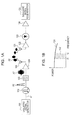
- FIG. 1A is a diagram illustrating an example of a configuration of an impulse radio communication apparatus according to an embodiment
- FIG. 1B is a diagram illustrating a pass frequency band of a band-pass filter 103.
- the impulse radio communication apparatus includes a baseband signal generator 101, a short-pulse generation unit 102, a band-pass filter 103, a transmission amplifier 104, a first antenna 105, a second antenna 121, a reception amplifier 122, a wave detector 123, a limit amplifier 124, and a baseband signal regenerator 125.
- the baseband signal generator 101, the short-pulse generation unit 102, the band-pass filter 103, the transmission amplifier 104, and the first antenna 105 constitute a transmission unit.
- the second antenna 121, the reception amplifier 122, the wave detector 123, the limit amplifier 124 and the baseband signal regenerator 125 constitute a reception unit.
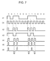
- the baseband signal generator 101 generates data signal A1 for each time slot, and outputs the signal to the short-pulse generation unit 102. As illustrated in FIG. 7 , the data signal A1 becomes a high level at the time of a value "1", and becomes a low level at the time of a value "0". A communication speed of the data signal A1 is, for example, 10 gigabits/second (Gbps).
- the short pulse generation unit 102 generates a short pulse A6 when the data signal A1 becomes the high level in a time slot.
- the band-pass filter 103 performs filtering on the short pulse A6 in order to pass only a predetermined pass frequency band, and outputs a millimeter-wave pulse A7.
- FIG. 1B illustrates a pass frequency band 132 of a band-pass filter 103.
- a short pulse characteristic 131 illustrates a frequency characteristic of the short pulse A6.
- the millimeter-wave pulse A7 has only frequency components of a part of the pass frequency band 132 among the short pulse characteristic 131.
- UWB Ultra Wide Band
- an available frequency band is limited.
- the band-pass filter 103 is used.
- the transmission amplifier 104 amplifies the millimeter-wave pulse A7, and radio-transmits a transmission signal A8 through the first antenna 105.
- the transmission signal A8 represents data of "1” or "0” depending on presence or absence of the millimeter-wave pulse.
- the reception amplifier 122 radio-receives a reception signal through the second antenna 121, and amplifies the reception signal.
- the wave detector 123 detects an envelope of the reception signal (millimeter-wave pulse) amplified by the reception amplifier 122, and outputs the signal.
- the limit amplifier 124 amplifies the signal detected by the wave detector 123.
- the baseband signal regenerator 125 receives input of the signal amplified by the limit amplifier 124, and reproduces receive data of 10 Gbps, for example.
- a radio communication apparatus of an impulse system may be used for a ultra-wideband radio communication apparatus, such as a microwave band, a quasi-millimeter wave band, and a UWB.
- the impulse system has a feature in which oscillators and mixers are not demanded, and thus a configuration of an RF unit becomes simple and low cost compared with a narrowband communication system. Accordingly, it is expected that broadband radio communication systems that perform broadband radio communication exceeding 10 Gbps are achieved in a millimeter wave band capable of using a broadband.
- a frequency band width assigned to an impulse radio communication apparatus is Bmax
- a pass frequency band width Bbpf of the band-pass filter 103 is equal to Bmax
- FIG. 2A is a diagram illustrating an example in which the short-pulse generation unit 102 generates a unipolar short pulse B6.
- the short pulse generator 102 generates a positive short pulse in a time slot in which the data signal A1 is a high level, and does not generate a positive short pulse in a time slot in which the data signal A1 is a low level, thereby outputting the unipolar short pulse B6.
- the unipolar short pulse B6 is a unipolar (for example, positive) short pulse.
- the band-pass filter 103 filters the unipolar short pulse B6, and outputs a millimeter-wave pulse B7.
- the millimeter-wave pulse B7 has a communication speed of 10 Gbps, and the time slot thereof is 100 ps.
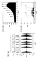
- FIG. 2B is a diagram illustrating a frequency spectrum of the millimeter-wave pulse B7 in FIG. 2A.
- FIG. 2C is an enlarged diagram of a part of FIG. 2B .
- the communication speed of the millimeter-wave pulse B7 is 10 Gbps
- bright line spectra BL occur at intervals of 10 GHz.
- the bright line spectrum BL is a linear large power spectrum, and for example, occurs at 30, 40, 50, 60, 70, 80, 90 GHz, etc.
- the bright line spectra BL appear at frequency intervals equal to the communication speed. For example, when the communication speed is 10 Gbps, the bright line spectra BL appear at intervals of 10 GHz.
- a transmission signal includes a bright line spectrum BL
- a signal intensity of the bright line spectrum BL infringes a limitation of the above-described power spectrum density, thereby resulting in a situation in which average power is not allowed to be increased in all frequency bands.
- FIG. 3 is a diagram illustrating examples of a unipolar short pulse B6 and the bipolar short pulse A6.
- the unipolar short pulse B6 is the same as the unipolar short pulse B6 in FIG. 2A .
- the short-pulse generation unit 102 receives input of the data signal A1, and generates the bipolar short pulse A6.
- the bipolar short pulse A6 represents presence and absence of a pulse in accordance with a value of the data signal A1, and is a pulse that alternately generates a positive pulse and a negative pulse.
- the bipolar short pulse A6 when the value of the data signal A1 is "1", a positive pulse or a negative pulse is generated as the bipolar short pulse A6, and when the value of the data signal A1 is "0", the bipolar short pulse A6 becomes a reference voltage.
- the positive pulse is a positive-voltage pulse with respect to the reference voltage
- the negative pulse is a negative-voltage pulse with respect to the reference voltage. That is to say, the bipolar short pulse A6 becomes a pulse having reverse polarity to an immediately preceding pulse.
- the bipolar short pulse A6 has only an inverted phase of a high frequency component with respect to the unipolar short pulse B6, and has a same envelope of the signal.
- the wave detector 123 in FIG. 1A detects the envelope of the reception signal. Accordingly, the reception unit of the impulse radio communication apparatus in FIG. 1A may have the same configuration in the case of receiving the unipolar short pulse B6 or in the case of receiving the bipolar short pulse A6.
- FIG. 4A is a diagram illustrating a power spectrum density of the bipolar short pulse A6.
- the communication speed of the transmission signal is 10 Gbps
- the time slot of the transmission signal is 100 ps.
- the power spectrum density of the bipolar short pulse A6 notches arise at frequencies equal to integer multiples of the communication speed (10 Gbps). That is to say, assuming that k is an integer, notches arise at frequencies of k ⁇ 10 GHz.
- the notch is a concave part that has a low power spectrum density.
- FIG. 4B is a diagram illustrating a power spectrum density of the output signal of the band-pass filter 103 that has received input of the unipolar short pulse B6.
- the unipolar short pulse B6 bright line spectra BL occur at frequencies equal to integer multiples of the communication speed (10 Gbps) in the same manner as FIG. 2B and FIG. 2C .
- bright line spectra BL occur at 60 GHz, 70 GHz and 80 GHz.
- FIG. 4C is a diagram illustrating a power spectrum density of the output signal A7 of the band-pass filter 103 that has received input of the bipolar short pulse A6.
- the bipolar short pulse A6 in the same manner as FIG. 4A , notches arise at frequencies equal to integer multiples of the communication speed (10 Gbps). For example, notches occur at 60 GHz, 70 GHz and 80 GHz.
- bright line spectra BL having frequencies equal to integer multiples of the communication speed (10 Gbps) are removed.
- bright line spectra BL will not arise, and thus it becomes easy to ensure transmission power, and thus it becomes advantageous to perform long-distance and high-quality communication.
- the transmission speed of the data signal is set to integer divisions of a difference between the upper-limit pass frequency f2 of the band-pass filter 103 and the lower-limit pass frequency f1.
- the upper limit frequency f2 is 90 GHz
- the lower limit frequency f1 is 80 GHz.
- the transmission speed of the data signal is set to integer divisions of 10 GHz.
- the transmission speed of the data signal may be set to 10 Gbps, 5 Gbps, 2 Gbps or 1 Gbps, etc.
- notches may be disposed at both of the ends f1 and f2 of the pass frequency band of the band-pass filter 103. Accordingly, it is possible to suppress irradiation of unwanted radio waves outside the allocated frequency band.
- the transmission speed is decreased, a frequency interval of notches becomes short, and the number of notches increases.
- FIG. 5 is a diagram illustrating an example of a configuration of the short-pulse generation unit 102 in the FIG. 1A
- FIG. 7 is a timing chart for explaining an example of operation of the short-pulse generation unit 102.
- the short-pulse generation unit 102 includes a nonreturn-to-zero (NRZ)/return-to-zero (RZ) conversion unit 501, a trigger flip-flop (T-FF) 502, and a short pulse generator 503.
- the data signal A1 is a nonreturn-to-zero signal.
- the nonreturn-to-zero (NRZ)/return-to-zero (RZ) conversion unit 501 converts the nonreturn-to-zero signal A1 into a return-to-zero signal A2.
- the nonreturn-to-zero (NRZ)/return-to-zero (RZ) conversion unit 501 is a logical product (AND) circuit, calculates a logical product of the nonreturn-to-zero signal A1 and the clock signal CK, and outputs the logical product signal as the return-to-zero signal A2.
- the trigger flip-flop 502 inverts an output signal A3 for each one cycle of the return-to-zero signal A2.
- a logical level of the output signal A3 is inverted for each one cycle of the return-to-zero signal A2, just like the high level ⁇ the low level ⁇ the high level.
- the output signal A3 is logically inverted in synchronism with a rising edge of the return-to-zero signal A2.
- the short pulse generator 503 receives input of the output signal A3 of the trigger flip-flop 502 and the return-to-zero signal A2, and shortens the pulse width of the return-to-zero signal A2, and outputs the signal A6 that alternately produces a positive pulse and a negative pulse to the band-pass filter 103.
- FIG. 6 is a circuit diagram illustrating an example of a configuration of the short pulse generator 503 in FIG. 5 .
- a delay circuit 601 outputs a signal A4, which is a delayed signal of the return-to-zero signal A2.
- a resistor 602 is connected between the ground potential node and a node of a signal /A5.
- a resistor 603 is connected between the ground potential node and a node of a signal A5.
- the signal A5 and the signal /A5 are differential signals whose phases are inverted with each other.
- a drain of an n-channel field-effect transistor 604 is connected to the node of the signal /A5, a gate thereof is connected to a bias potential node, and a source thereof is connected to a drain of an n-channel field-effect transistor 606.
- a drain of an n-channel field-effect transistor 605 is connected to a node of the signal A5, a gate thereof is connected to the bias potential node, and a source thereof is connected to a drain of an n-channel field-effect transistor 607.
- a gate of the n-channel field-effect transistor 606 is connected to a node of the return-to-zero signal A2, and a source thereof is connected to a drain of an n-channel field-effect transistor 610.
- a gate of the n-channel field-effect transistor 607 is connected to, for example, a potential node of -2 V, a source thereof is connected to the drain of the n-channel field-effect transistor 610.
- the transistor 604 and the transistor 605 constitute common-gate cascode amplifiers, respectively.
- a gate of the n-channel field-effect transistor 610 is connected the node of the signal A4, and a source thereof is connected to a drain of an n-channel field-effect transistor 612.
- a drain of an n-channel field-effect transistor 608 is connected to a drain of the n-channel field-effect transistor 606, a gate thereof is connected to, for example, a potential node of -1.7 V, and a source thereof is connected to a drain of an n-channel field-effect transistor 611.
- a drain of an n-channel field-effect transistor 609 is connected to the drain of the n-channel field-effect transistor 607, a gate thereof is connected to, for example, a potential node of -2.3 V, and a source thereof is connected to a drain of the n-channel field-effect transistor 611.
- a gate of the n-channel field-effect transistor 611 is connected to, for example, a potential node of -2.4 V, a source thereof is connected to a drain of an n-channel field-effect transistor 612.
- the n-channel field-effect transistor 612 is a current source, a gate thereof is connected to a bias potential node, and a source thereof is connected to, for example, a potential node of -2.6 V.
- a resistor 613 is connected between the ground potential node and a node of the signal A6.
- the resistor 614 is connected between the ground potential node and a node of the signal /A6.
- the signal A6 and the signal /A6 are differential signals whose phases are inverted with each other.
- a drain of an n-channel field-effect transistor 615 is connected to a node of the signal A6, a gate thereof is connected to a node of the signal A3, and a source thereof is connected to a drain of an n-channel field-effect transistor 619.
- a drain of an n-channel field-effect transistor 616 is connected to a node of the signal /A6, a gate thereof is connected to a node of signal /A3, and a source thereof is connected to a drain of the n-channel field-effect transistor 619.
- the signal A3 and the signal /A3 are differential signals whose phases are inverted with each other.
- a gate of the n-channel field-effect transistor 619 is connected to a node of the signal /A5, and a source thereof is connected to a drain of an n-channel field-effect transistor 621.
- a drain of an n-channel field-effect transistor 617 is connected to a node of the signal A6, a gate thereof is connected to a bias potential node, and a source thereof is connected to a drain of an n-channel field-effect transistor 620.
- a drain of an n-channel field-effect transistor 618 is connected to a node of the signal /A6, a gate thereof is connected to a bias potential node, and a source thereof is connected to the drain of the n-channel field-effect transistor 620.
- a gate of the n-channel field-effect transistor 620 is connected to the node of the signal A5, a source thereof is connected to the drain of the n-channel field-effect transistor 621.
- the n-channel field-effect transistor 621 is a current source, a gate thereof is connected to a bias potential node, and a source thereof is connected to, for example, a potential node of -2.6 V.
- the signal A5 is a logical product signal of the return-to-zero signal A2 and the delay signal A4.
- the signal A3 is a high level
- the signal A5 becomes a high level pulse
- the signal A6 becomes a positive pulse.
- the signal A3 is a low level
- the signal A5 becomes a high level pulse
- the signal A6 becomes a negative pulse.
- the bipolar short pulse A6 has, for example, a reference voltage of -0.4 V, and alternately produces a positive pulse of 0 V and a negative pulse of -0.8 V.
- the transmission signal does not includes a bright line spectrum BL, and thus the transmission signal is not subject to a power limitation by the bright line spectrum BL. Accordingly, it is possible to ensure a large transmission power to obtain a high communication margin (S/N), and thereby there is an advantage in that it becomes easy to achieve long-distance and high-quality communication of the signal. Also, by suitably setting a communication speed for an allocated frequency band, and disposing notches at both ends of the allocated frequency band width, there is an advantage of reducing irradiation of unwanted power outside the allocated frequency band.
- the reception unit it is possible to configure the reception unit for receiving the bipolar short pulse A6 in the same manner as a reception unit for receiving the unipolar short pulse B6, and thus it is possible to suppress an increase in installation cost to a minimum.
Landscapes
- Engineering & Computer Science (AREA)
- Computer Networks & Wireless Communication (AREA)
- Signal Processing (AREA)
- Physics & Mathematics (AREA)
- Spectroscopy & Molecular Physics (AREA)
- Electromagnetism (AREA)
- Power Engineering (AREA)
- Transmitters (AREA)
Abstract
Description
- The embodiments discussed herein are related to a communication apparatus.
- Impulse radio communication is radio communication using a short pulse, and is expected to be applied to broadband radio communication systems.
- Also, a U/B conversion circuit, which is a U/B conversion circuit that converts a unipolar signal into a bipolar signal, and when a signal produced by performing NRZ/RZ conversion on an input NRZ signal is given, a bipolar signal produced by converting an NRZ signal is obtained as an emitter output of a transistor, is known.
- Also, a pulse-polarity modulation circuit in which pairs of differential transistors are stacked in two-stages, and a unipolar pulse is converted into a bipolar pulse in accordance with a value of the input data, is known.
-
- [Patent Document] Japanese Laid-open Patent Publication No.
3-27622 - [Patent Document] Japanese Laid-open Patent Publication No.
2006-157649 - The purpose of the invention is providing a communication apparatus to eliminate the bright line spectrum from the transmission signal.
- According to an aspect of the embodiments, a communication apparatus includes: a pulse generation unit configured to alternately generate a positive pulse and a negative pulse indicating presence or absence of a pulse in accordance with a value of a data signal; a band-pass filter configured to filter the pulse generated by the pulse generator; and a transmission amplifier configured to amplify a signal filtered by the band-pass filter, and to output the signal as a transmission signal.
-
-
FIG. 1A is a diagram illustrating an example of a configuration of an impulse radio communication apparatus according to an embodiment, andFIG. 1B is a diagram illustrating a pass frequency band of a band-pass filter; -
FIGs. 2A to 2C are diagrams illustrating examples in which a short-pulse generation unit generates a unipolar short pulse; -
FIG. 3 is a diagram illustrating examples of a unipolar short pulse and a bipolar short pulse; -
FIGs. 4A to 4C are diagrams illustrating power spectrum densities of a unipolar short pulse and a bipolar short pulse; -
FIG. 5 is a diagram illustrating an example of a configuration of the short-pulse generation unit in theFIG. 1A ; -
FIG. 6 is a circuit diagram illustrating an example of a configuration of the short pulse generator inFIG. 5 ; and -
FIG. 7 is a timing chart for describing an example of operation of the short-pulse generation unit. -
FIG. 1A is a diagram illustrating an example of a configuration of an impulse radio communication apparatus according to an embodiment, andFIG. 1B is a diagram illustrating a pass frequency band of a band-pass filter 103. The impulse radio communication apparatus includes abaseband signal generator 101, a short-pulse generation unit 102, a band-pass filter 103, atransmission amplifier 104, afirst antenna 105, asecond antenna 121, areception amplifier 122, awave detector 123, alimit amplifier 124, and abaseband signal regenerator 125. - The
baseband signal generator 101, the short-pulse generation unit 102, the band-pass filter 103, thetransmission amplifier 104, and thefirst antenna 105 constitute a transmission unit. On the other hand, thesecond antenna 121, thereception amplifier 122, thewave detector 123, thelimit amplifier 124 and thebaseband signal regenerator 125 constitute a reception unit. - First, a description will be given of the transmission unit. The
baseband signal generator 101 generates data signal A1 for each time slot, and outputs the signal to the short-pulse generation unit 102. As illustrated inFIG. 7 , the data signal A1 becomes a high level at the time of a value "1", and becomes a low level at the time of a value "0". A communication speed of the data signal A1 is, for example, 10 gigabits/second (Gbps). The shortpulse generation unit 102 generates a short pulse A6 when the data signal A1 becomes the high level in a time slot. The band-pass filter 103 performs filtering on the short pulse A6 in order to pass only a predetermined pass frequency band, and outputs a millimeter-wave pulse A7. -
FIG. 1B illustrates apass frequency band 132 of a band-pass filter 103. Ashort pulse characteristic 131 illustrates a frequency characteristic of the short pulse A6. The millimeter-wave pulse A7 has only frequency components of a part of thepass frequency band 132 among theshort pulse characteristic 131. In UWB (Ultra Wide Band), etc., an available frequency band is limited. In order to satisfy a limitation of the frequency band, the band-pass filter 103 is used. Thepass frequency band 132 has, for example, a lower-limit pass frequency f1 of 80 GHz, and an upper-limit pass frequency f2 of 90 GHz, and thus the pass frequency band width is f2 - f1 = 90 - 80 = 10 GHz. - The
transmission amplifier 104 amplifies the millimeter-wave pulse A7, and radio-transmits a transmission signal A8 through thefirst antenna 105. The transmission signal A8 represents data of "1" or "0" depending on presence or absence of the millimeter-wave pulse. - Next, a description will be given of the reception unit. The reception amplifier 122 radio-receives a reception signal through the
second antenna 121, and amplifies the reception signal. Thewave detector 123 detects an envelope of the reception signal (millimeter-wave pulse) amplified by thereception amplifier 122, and outputs the signal. Thelimit amplifier 124 amplifies the signal detected by thewave detector 123. Thebaseband signal regenerator 125 receives input of the signal amplified by thelimit amplifier 124, and reproduces receive data of 10 Gbps, for example. - A radio communication apparatus of an impulse system may be used for a ultra-wideband radio communication apparatus, such as a microwave band, a quasi-millimeter wave band, and a UWB. The impulse system has a feature in which oscillators and mixers are not demanded, and thus a configuration of an RF unit becomes simple and low cost compared with a narrowband communication system. Accordingly, it is expected that broadband radio communication systems that perform broadband radio communication exceeding 10 Gbps are achieved in a millimeter wave band capable of using a broadband.
- If it is assumed that a frequency band width assigned to an impulse radio communication apparatus is Bmax, if a pass frequency band width Bbpf of the band-
pass filter 103 is equal to Bmax, the maximum communication speed Bmax is obtained. For example, if the frequency band width Bmax is 10 GHz, as illustrated inFIG. 1B , the pass frequency band width Bbpf of the band-pass filter 103 is f2 - f1 = 90 - 80 = 10 GHz, and the communication speed of the data signal is 10 Gbps. -
FIG. 2A is a diagram illustrating an example in which the short-pulse generation unit 102 generates a unipolar short pulse B6. Theshort pulse generator 102 generates a positive short pulse in a time slot in which the data signal A1 is a high level, and does not generate a positive short pulse in a time slot in which the data signal A1 is a low level, thereby outputting the unipolar short pulse B6. The unipolar short pulse B6 is a unipolar (for example, positive) short pulse. The band-pass filter 103 filters the unipolar short pulse B6, and outputs a millimeter-wave pulse B7. For example, the millimeter-wave pulse B7 has a communication speed of 10 Gbps, and the time slot thereof is 100 ps. -
FIG. 2B is a diagram illustrating a frequency spectrum of the millimeter-wave pulse B7 inFIG. 2A. FIG. 2C is an enlarged diagram of a part ofFIG. 2B . If the communication speed of the millimeter-wave pulse B7 is 10 Gbps, bright line spectra BL occur at intervals of 10 GHz. The bright line spectrum BL is a linear large power spectrum, and for example, occurs at 30, 40, 50, 60, 70, 80, 90 GHz, etc. The bright line spectra BL appear at frequency intervals equal to the communication speed. For example, when the communication speed is 10 Gbps, the bright line spectra BL appear at intervals of 10 GHz. - Incidentally, for many radio communication apparatuses, a signal intensity for each unit frequency (power spectrum density) is defined by law or by standards, etc., such as a
signal intensity 0 dBm for each 1 MHz frequency (= 1 mW/MHz), for example. If a transmission signal includes a bright line spectrum BL, a signal intensity of the bright line spectrum BL infringes a limitation of the above-described power spectrum density, thereby resulting in a situation in which average power is not allowed to be increased in all frequency bands. Specifically, when the allocated frequency band Bmax is 10 GHz (= 10000 MHz), if a transmission spectrum intensity is fixed in a frequency band, it becomes possible to output 1 (mW/MHz) × 10000 (MHz) = 10 W. However, if a bright line spectrum BL of 1 mW/MHz is included in the transmission signal, only small power may be output. In order to perform long distance transmission without a signal error, it is demanded to maximize a spectrum power for all the frequency bands, and to ensure a signal intensity margin against noise, etc., (SN ratio). If the transmission power is restricted because of a bright line spectrum BL, it is difficult to sufficiently ensure the SN ratio. In this manner, the transmission power is restricted by a bright line spectrum BL, and long-distance and high-quality communication becomes disadvantageous, and thus it is a task to achieve an impulse radio communication apparatus that does not produce a bright line spectrum BL. In the following, a description will be given of an embodiment of an impulse-radio communication apparatus that produces a transmission signal not including a bright line spectrum BL, and that is suitable for long-distance and high-quality communications. -
FIG. 3 is a diagram illustrating examples of a unipolar short pulse B6 and the bipolar short pulse A6. The unipolar short pulse B6 is the same as the unipolar short pulse B6 inFIG. 2A . In the present embodiment, the short-pulse generation unit 102 receives input of the data signal A1, and generates the bipolar short pulse A6. The bipolar short pulse A6 represents presence and absence of a pulse in accordance with a value of the data signal A1, and is a pulse that alternately generates a positive pulse and a negative pulse. For example, when the value of the data signal A1 is "1", a positive pulse or a negative pulse is generated as the bipolar short pulse A6, and when the value of the data signal A1 is "0", the bipolar short pulse A6 becomes a reference voltage. The positive pulse is a positive-voltage pulse with respect to the reference voltage, and the negative pulse is a negative-voltage pulse with respect to the reference voltage. That is to say, the bipolar short pulse A6 becomes a pulse having reverse polarity to an immediately preceding pulse. - The bipolar short pulse A6 has only an inverted phase of a high frequency component with respect to the unipolar short pulse B6, and has a same envelope of the signal. The
wave detector 123 inFIG. 1A detects the envelope of the reception signal. Accordingly, the reception unit of the impulse radio communication apparatus inFIG. 1A may have the same configuration in the case of receiving the unipolar short pulse B6 or in the case of receiving the bipolar short pulse A6. -
FIG. 4A is a diagram illustrating a power spectrum density of the bipolar short pulse A6. Here, the communication speed of the transmission signal is 10 Gbps, and the time slot of the transmission signal is 100 ps. In the power spectrum density of the bipolar short pulse A6, notches arise at frequencies equal to integer multiples of the communication speed (10 Gbps). That is to say, assuming that k is an integer, notches arise at frequencies of k × 10 GHz. The notch is a concave part that has a low power spectrum density. -
FIG. 4B is a diagram illustrating a power spectrum density of the output signal of the band-pass filter 103 that has received input of the unipolar short pulse B6. In the case of the unipolar short pulse B6, bright line spectra BL occur at frequencies equal to integer multiples of the communication speed (10 Gbps) in the same manner asFIG. 2B and FIG. 2C . For example, bright line spectra BL occur at 60 GHz, 70 GHz and 80 GHz. -
FIG. 4C is a diagram illustrating a power spectrum density of the output signal A7 of the band-pass filter 103 that has received input of the bipolar short pulse A6. In the case of the bipolar short pulse A6, in the same manner asFIG. 4A , notches arise at frequencies equal to integer multiples of the communication speed (10 Gbps). For example, notches occur at 60 GHz, 70 GHz and 80 GHz. As a result, bright line spectra BL having frequencies equal to integer multiples of the communication speed (10 Gbps) are removed. In the present embodiment, bright line spectra BL will not arise, and thus it becomes easy to ensure transmission power, and thus it becomes advantageous to perform long-distance and high-quality communication. Further, by setting a suitable communication speed for an allocated frequency band, it is possible to dispose notches at both ends f1 and f2 of the pass frequency band of the band-pass filter 103. Accordingly, it becomes advantageous to suppress irradiation of unwanted radio waves outside the allocated frequency band. - The transmission speed of the data signal is set to integer divisions of a difference between the upper-limit pass frequency f2 of the band-
pass filter 103 and the lower-limit pass frequency f1. For example, the upper limit frequency f2 is 90 GHz, and the lower limit frequency f1 is 80 GHz. The pass frequency bandwidth of the band-pass filter 103 is f2 - f1 = 90 - 80 = 10 GHz. In this case, the transmission speed of the data signal is set to integer divisions of 10 GHz. For example, the transmission speed of the data signal may be set to 10 Gbps, 5 Gbps, 2 Gbps or 1 Gbps, etc. In this manner, by setting a transmission speed, notches may be disposed at both of the ends f1 and f2 of the pass frequency band of the band-pass filter 103. Accordingly, it is possible to suppress irradiation of unwanted radio waves outside the allocated frequency band. In this regard, as the transmission speed is decreased, a frequency interval of notches becomes short, and the number of notches increases. -
FIG. 5 is a diagram illustrating an example of a configuration of the short-pulse generation unit 102 in theFIG. 1A , andFIG. 7 is a timing chart for explaining an example of operation of the short-pulse generation unit 102. The short-pulse generation unit 102 includes a nonreturn-to-zero (NRZ)/return-to-zero (RZ)conversion unit 501, a trigger flip-flop (T-FF) 502, and ashort pulse generator 503. The data signal A1 is a nonreturn-to-zero signal. The nonreturn-to-zero (NRZ)/return-to-zero (RZ)conversion unit 501 converts the nonreturn-to-zero signal A1 into a return-to-zero signal A2. Specifically, the nonreturn-to-zero (NRZ)/return-to-zero (RZ)conversion unit 501 is a logical product (AND) circuit, calculates a logical product of the nonreturn-to-zero signal A1 and the clock signal CK, and outputs the logical product signal as the return-to-zero signal A2. The trigger flip-flop 502 inverts an output signal A3 for each one cycle of the return-to-zero signal A2. For example, a logical level of the output signal A3 is inverted for each one cycle of the return-to-zero signal A2, just like the high level → the low level → the high level. Specifically, the output signal A3 is logically inverted in synchronism with a rising edge of the return-to-zero signal A2. Theshort pulse generator 503 receives input of the output signal A3 of the trigger flip-flop 502 and the return-to-zero signal A2, and shortens the pulse width of the return-to-zero signal A2, and outputs the signal A6 that alternately produces a positive pulse and a negative pulse to the band-pass filter 103. -
FIG. 6 is a circuit diagram illustrating an example of a configuration of theshort pulse generator 503 inFIG. 5 . Adelay circuit 601 outputs a signal A4, which is a delayed signal of the return-to-zero signal A2. Aresistor 602 is connected between the ground potential node and a node of a signal /A5. Aresistor 603 is connected between the ground potential node and a node of a signal A5. The signal A5 and the signal /A5 are differential signals whose phases are inverted with each other. A drain of an n-channel field-effect transistor 604 is connected to the node of the signal /A5, a gate thereof is connected to a bias potential node, and a source thereof is connected to a drain of an n-channel field-effect transistor 606. A drain of an n-channel field-effect transistor 605 is connected to a node of the signal A5, a gate thereof is connected to the bias potential node, and a source thereof is connected to a drain of an n-channel field-effect transistor 607. A gate of the n-channel field-effect transistor 606 is connected to a node of the return-to-zero signal A2, and a source thereof is connected to a drain of an n-channel field-effect transistor 610. A gate of the n-channel field-effect transistor 607 is connected to, for example, a potential node of -2 V, a source thereof is connected to the drain of the n-channel field-effect transistor 610. Thetransistor 604 and thetransistor 605 constitute common-gate cascode amplifiers, respectively. A gate of the n-channel field-effect transistor 610 is connected the node of the signal A4, and a source thereof is connected to a drain of an n-channel field-effect transistor 612. - A drain of an n-channel field-
effect transistor 608 is connected to a drain of the n-channel field-effect transistor 606, a gate thereof is connected to, for example, a potential node of -1.7 V, and a source thereof is connected to a drain of an n-channel field-effect transistor 611. A drain of an n-channel field-effect transistor 609 is connected to the drain of the n-channel field-effect transistor 607, a gate thereof is connected to, for example, a potential node of -2.3 V, and a source thereof is connected to a drain of the n-channel field-effect transistor 611. A gate of the n-channel field-effect transistor 611 is connected to, for example, a potential node of -2.4 V, a source thereof is connected to a drain of an n-channel field-effect transistor 612. The n-channel field-effect transistor 612 is a current source, a gate thereof is connected to a bias potential node, and a source thereof is connected to, for example, a potential node of -2.6 V. - A
resistor 613 is connected between the ground potential node and a node of the signal A6. Theresistor 614 is connected between the ground potential node and a node of the signal /A6. The signal A6 and the signal /A6 are differential signals whose phases are inverted with each other. A drain of an n-channel field-effect transistor 615 is connected to a node of the signal A6, a gate thereof is connected to a node of the signal A3, and a source thereof is connected to a drain of an n-channel field-effect transistor 619. A drain of an n-channel field-effect transistor 616 is connected to a node of the signal /A6, a gate thereof is connected to a node of signal /A3, and a source thereof is connected to a drain of the n-channel field-effect transistor 619. The signal A3 and the signal /A3 are differential signals whose phases are inverted with each other. A gate of the n-channel field-effect transistor 619 is connected to a node of the signal /A5, and a source thereof is connected to a drain of an n-channel field-effect transistor 621. - A drain of an n-channel field-
effect transistor 617 is connected to a node of the signal A6, a gate thereof is connected to a bias potential node, and a source thereof is connected to a drain of an n-channel field-effect transistor 620. A drain of an n-channel field-effect transistor 618 is connected to a node of the signal /A6, a gate thereof is connected to a bias potential node, and a source thereof is connected to the drain of the n-channel field-effect transistor 620. A gate of the n-channel field-effect transistor 620 is connected to the node of the signal A5, a source thereof is connected to the drain of the n-channel field-effect transistor 621. The n-channel field-effect transistor 621 is a current source, a gate thereof is connected to a bias potential node, and a source thereof is connected to, for example, a potential node of -2.6 V. - The signal A5 is a logical product signal of the return-to-zero signal A2 and the delay signal A4. When the signal A3 is a high level, if the signal A5 becomes a high level pulse, the signal A6 becomes a positive pulse. On the other hand, when the signal A3 is a low level, if the signal A5 becomes a high level pulse, the signal A6 becomes a negative pulse. The bipolar short pulse A6 has, for example, a reference voltage of -0.4 V, and alternately produces a positive pulse of 0 V and a negative pulse of -0.8 V.
- By the present embodiment, the transmission signal does not includes a bright line spectrum BL, and thus the transmission signal is not subject to a power limitation by the bright line spectrum BL. Accordingly, it is possible to ensure a large transmission power to obtain a high communication margin (S/N), and thereby there is an advantage in that it becomes easy to achieve long-distance and high-quality communication of the signal. Also, by suitably setting a communication speed for an allocated frequency band, and disposing notches at both ends of the allocated frequency band width, there is an advantage of reducing irradiation of unwanted power outside the allocated frequency band. In the reception unit, it is possible to configure the reception unit for receiving the bipolar short pulse A6 in the same manner as a reception unit for receiving the unipolar short pulse B6, and thus it is possible to suppress an increase in installation cost to a minimum.
- In this regard, all of the above-described embodiment is only an example of implementing the present disclosure, and it is to be understood that a technical scope of the present disclosure be not limited by the description. That is to say, it is possible to carry out the present disclosure in various ways without departing from the spirit and scope of the present disclosure.
Claims (10)
- A communication apparatus comprising:a pulse generation unit configured to alternately generate a positive pulse and a negative pulse indicating presence or absence of a pulse in accordance with a value of a data signal;a band-pass filter configured to filter the pulse generated by the pulse generator; anda transmission amplifier configured to amplify a signal filtered by the band-pass filter, and to output the signal as a transmission signal.
- The communication apparatus according to Claim 1,
wherein the pulse generation unit includes a nonreturn-to-zero/return-to-zero conversion unit configured to convert the data signal from a nonreturn-to-zero signal to a return-to-zero signal. - The communication apparatus according to Claim 1,
wherein the pulse generation unit includes a pulse generator configured to shorten a pulse width of a return-to-zero signal, and to alternately generate the positive pulse and the negative pulse. - The communication apparatus according to Claim 3,
wherein the pulse generation unit includes a trigger flip-flop configured to invert an output signal for each one cycle of the return-to-zero signal, and
the pulse generator receives the output signal of the trigger flip-flop and the return-to-zero signal. - The communication apparatus according to Claim 1,
wherein the pulse generation unit includes
a nonreturn-to-zero/return-to-zero conversion unit configured to convert the data signal from a nonreturn-to-zero signal to a return-to-zero signal, and
a pulse generator configured to shorten a pulse width of the return-to-zero signal, and to alternately generate the positive pulse and the negative pulse. - The communication apparatus according to Claim 5,
wherein the pulse generation unit includes a trigger flip-flop configured to invert an output signal for each one cycle of the return-to-zero signal, and
the pulse generator receives the output signal of the trigger flip-flop and the return-to-zero signal. - The communication apparatus according to any preceding claim,
wherein a transmission speed of the data signal is one of integer divisions of a difference between an upper-limit pass frequency and a lower-limit pass frequency of the band-pass filter. - The communication apparatus according to any preceding claim, further comprising
a first antenna for radio-transmitting the transmission signal amplified by the transmission amplifier. - The communication apparatus according to any preceding claim, further comprising
a reception amplifier configured to amplify a reception signal, and
a wave detector configured to detect the reception signal amplified by the reception amplifier. - The communication apparatus according to Claim 9, further comprising
a second antenna for radio receiving the reception signal,
wherein the reception amplifier amplifies the reception signal radio-received by the second antenna.
Applications Claiming Priority (1)
| Application Number | Priority Date | Filing Date | Title |
|---|---|---|---|
| JP2011168641A JP5741296B2 (en) | 2011-08-01 | 2011-08-01 | Communication device |
Publications (2)
| Publication Number | Publication Date |
|---|---|
| EP2555440A1 true EP2555440A1 (en) | 2013-02-06 |
| EP2555440B1 EP2555440B1 (en) | 2016-05-25 |
Family
ID=46796255
Family Applications (1)
| Application Number | Title | Priority Date | Filing Date |
|---|---|---|---|
| EP12177938.3A Not-in-force EP2555440B1 (en) | 2011-08-01 | 2012-07-26 | Impulse radio communication apparatus |
Country Status (3)
| Country | Link |
|---|---|
| US (1) | US9184789B2 (en) |
| EP (1) | EP2555440B1 (en) |
| JP (1) | JP5741296B2 (en) |
Cited By (1)
| Publication number | Priority date | Publication date | Assignee | Title |
|---|---|---|---|---|
| EP2621099A1 (en) * | 2012-01-26 | 2013-07-31 | Fujitsu Limited | Communication device |
Families Citing this family (4)
| Publication number | Priority date | Publication date | Assignee | Title |
|---|---|---|---|---|
| JP5991243B2 (en) * | 2013-03-18 | 2016-09-14 | 富士通株式会社 | Transmitter |
| JP2014195217A (en) * | 2013-03-29 | 2014-10-09 | Nippon Telegr & Teleph Corp <Ntt> | Communication system and communication method |
| JP2014195216A (en) * | 2013-03-29 | 2014-10-09 | Nippon Telegr & Teleph Corp <Ntt> | Communication system and communication method |
| JP6149937B2 (en) | 2013-10-02 | 2017-06-21 | 富士通株式会社 | Pulse position modulation type impulse radio transmitter and radio communication system |
Citations (3)
| Publication number | Priority date | Publication date | Assignee | Title |
|---|---|---|---|---|
| JPH0327622A (en) | 1989-06-26 | 1991-02-06 | Fujitsu Ltd | U/b conversion circuit |
| JP2006157649A (en) | 2004-11-30 | 2006-06-15 | Fujitsu Ltd | Pulse polarity modulation circuit |
| US20080198939A1 (en) * | 2007-02-19 | 2008-08-21 | Fujitsu Limited | Transmitter circuit and radio transmission apparatus for transmitting data via radio by using impulses |
Family Cites Families (17)
| Publication number | Priority date | Publication date | Assignee | Title |
|---|---|---|---|---|
| US4419757A (en) * | 1981-03-16 | 1983-12-06 | Bell Telephone Laboratories, Incorporated | Transformerless bipolar converter |
| US4504944A (en) * | 1982-05-13 | 1985-03-12 | At&T Bell Laboratories | Bridging channel port module |
| FI97010C (en) * | 1987-05-29 | 1996-09-25 | Nec Corp | Control station and radio communication network system including switching device units operating in different operating modes |
| US5365551A (en) * | 1992-12-15 | 1994-11-15 | Micron Technology, Inc. | Data communication transceiver using identification protocol |
| JP3152292B2 (en) * | 1997-04-15 | 2001-04-03 | 日本電気株式会社 | Method and apparatus for removing multi-channel echo |
| US6020765A (en) * | 1997-05-30 | 2000-02-01 | Sun Microsystems, Inc. | Frequency difference detector for use with an NRZ signal |
| US6218842B1 (en) * | 1999-08-04 | 2001-04-17 | Halliburton Energy Services, Inc. | Multi-frequency electromagnetic wave resistivity tool with improved calibration measurement |
| US6665500B2 (en) * | 2001-01-29 | 2003-12-16 | Oyster Optics, Inc. | Dual-mode fiber optic telecommunications system and method |
| WO2003088568A2 (en) * | 2002-04-12 | 2003-10-23 | Thomson Licensing S.A. | Digital control circuit for serial uart transmissions |
| JP3705271B2 (en) * | 2003-02-03 | 2005-10-12 | ソニー株式会社 | Transmission method and transmission apparatus |
| US7298792B2 (en) | 2003-02-10 | 2007-11-20 | Mitsubishi Electric Research Laboratories, Inc. | Randomly changing pulse polarity and phase in an UWB signal for power spectrum density shaping |
| US7636380B2 (en) * | 2004-05-17 | 2009-12-22 | Microsoft Corporation | Orthogonal pulse polarity modulation |
| US20060066485A1 (en) * | 2004-09-24 | 2006-03-30 | Guohua Min | Wireless tracking system based upon phase differences |
| JP4408091B2 (en) * | 2005-04-18 | 2010-02-03 | 日本電信電話株式会社 | Wireless transmission method and wireless transmitter |
| US8332680B2 (en) * | 2007-08-13 | 2012-12-11 | Rambus Inc. | Methods and systems for operating memory in two modes |
| US20110141829A1 (en) * | 2009-12-14 | 2011-06-16 | Ware Frederick A | Circuits for Reducing Power Consumption of Memory Components |
| US8867930B2 (en) * | 2010-10-29 | 2014-10-21 | Queen's University At Kingston | System and method for determining the envelope of a modulated signal |
-
2011
- 2011-08-01 JP JP2011168641A patent/JP5741296B2/en not_active Expired - Fee Related
-
2012
- 2012-07-26 EP EP12177938.3A patent/EP2555440B1/en not_active Not-in-force
- 2012-07-27 US US13/559,883 patent/US9184789B2/en not_active Expired - Fee Related
Patent Citations (3)
| Publication number | Priority date | Publication date | Assignee | Title |
|---|---|---|---|---|
| JPH0327622A (en) | 1989-06-26 | 1991-02-06 | Fujitsu Ltd | U/b conversion circuit |
| JP2006157649A (en) | 2004-11-30 | 2006-06-15 | Fujitsu Ltd | Pulse polarity modulation circuit |
| US20080198939A1 (en) * | 2007-02-19 | 2008-08-21 | Fujitsu Limited | Transmitter circuit and radio transmission apparatus for transmitting data via radio by using impulses |
Cited By (2)
| Publication number | Priority date | Publication date | Assignee | Title |
|---|---|---|---|---|
| EP2621099A1 (en) * | 2012-01-26 | 2013-07-31 | Fujitsu Limited | Communication device |
| US8948299B2 (en) | 2012-01-26 | 2015-02-03 | Fujitsu Limited | Pulse converting and shaping communication device |
Also Published As
| Publication number | Publication date |
|---|---|
| JP2013034075A (en) | 2013-02-14 |
| US9184789B2 (en) | 2015-11-10 |
| US20130034131A1 (en) | 2013-02-07 |
| EP2555440B1 (en) | 2016-05-25 |
| JP5741296B2 (en) | 2015-07-01 |
Similar Documents
| Publication | Publication Date | Title |
|---|---|---|
| US8948299B2 (en) | Pulse converting and shaping communication device | |
| KR100944774B1 (en) | Transmission circuit and wireless transmission device | |
| EP2555440B1 (en) | Impulse radio communication apparatus | |
| KR101744202B1 (en) | Method and apparatus for generating pulse | |
| JP5104712B2 (en) | Transmitter | |
| Lee et al. | Reconfigurable 60-GHz radar transmitter SoC with broadband frequency tripler in 45nm SOI CMOS | |
| US8437377B2 (en) | Pulse generator, transmitter-receiver, and pulse generation method | |
| US9325557B2 (en) | Radio communication apparatus and pulse signal transmission method in radio communication apparatus | |
| US20160211884A1 (en) | Pulse position modulation scheme impulse radio transmitter and radio communication system | |
| JP5459369B2 (en) | Transmitter | |
| Daoud et al. | Design of an OOK IR-UWB front-end for biomedical devices | |
| Xie et al. | A varying pulse width second order derivative Gaussian pulse generator for UWB transceivers in CMOS | |
| Majidzadeh et al. | An 8-PPM, 45 pJ/bit UWB transmitter with reduced number of PA elements | |
| JP4408092B2 (en) | Wireless communication method, wireless transmission method, wireless communication system, and wireless transmitter | |
| US7321608B2 (en) | Process and device for generating pulses for the transmission of a pulsed signal of the ultra wideband type | |
| JP5041406B2 (en) | Ultra-wideband wireless communication device | |
| JP5367861B2 (en) | Ultra-wideband wireless communication device | |
| JP5077147B2 (en) | Signal generator | |
| RU2128396C1 (en) | Method for information reception and transmission and device which implements said method | |
| Jin et al. | An UWB millimeter-wave transceiver architecture for Wireless Sensor Networks applications | |
| Chen et al. | Fully integrated CMOS UWB transmitter for application in China | |
| Vaithianathan et al. | Design and simulation of pulse generator for Ultra Wide Band impulse radio | |
| Kolakowski | Application of quadrature mixing for I-UWB signal spectrum shaping | |
| JP2019036894A (en) | Impulse wireless communication apparatus and impulse wireless communication system | |
| Kikkawa | A single-chip Gaussian monocycle pulse transmitter with on-chip integrated antennas using 0.18 μm CMOS technology |
Legal Events
| Date | Code | Title | Description |
|---|---|---|---|
| PUAI | Public reference made under article 153(3) epc to a published international application that has entered the european phase |
Free format text: ORIGINAL CODE: 0009012 |
|
| AK | Designated contracting states |
Kind code of ref document: A1 Designated state(s): AL AT BE BG CH CY CZ DE DK EE ES FI FR GB GR HR HU IE IS IT LI LT LU LV MC MK MT NL NO PL PT RO RS SE SI SK SM TR |
|
| AX | Request for extension of the european patent |
Extension state: BA ME |
|
| 17P | Request for examination filed |
Effective date: 20130617 |
|
| RBV | Designated contracting states (corrected) |
Designated state(s): AL AT BE BG CH CY CZ DE DK EE ES FI FR GB GR HR HU IE IS IT LI LT LU LV MC MK MT NL NO PL PT RO RS SE SI SK SM TR |
|
| GRAP | Despatch of communication of intention to grant a patent |
Free format text: ORIGINAL CODE: EPIDOSNIGR1 |
|
| RIC1 | Information provided on ipc code assigned before grant |
Ipc: H04B 1/717 20110101AFI20151130BHEP Ipc: H04L 25/03 20060101ALI20151130BHEP |
|
| INTG | Intention to grant announced |
Effective date: 20151215 |
|
| GRAS | Grant fee paid |
Free format text: ORIGINAL CODE: EPIDOSNIGR3 |
|
| GRAA | (expected) grant |
Free format text: ORIGINAL CODE: 0009210 |
|
| AK | Designated contracting states |
Kind code of ref document: B1 Designated state(s): AL AT BE BG CH CY CZ DE DK EE ES FI FR GB GR HR HU IE IS IT LI LT LU LV MC MK MT NL NO PL PT RO RS SE SI SK SM TR |
|
| REG | Reference to a national code |
Ref country code: GB Ref legal event code: FG4D |
|
| REG | Reference to a national code |
Ref country code: CH Ref legal event code: EP |
|
| REG | Reference to a national code |
Ref country code: FR Ref legal event code: PLFP Year of fee payment: 5 |
|
| REG | Reference to a national code |
Ref country code: IE Ref legal event code: FG4D Ref country code: AT Ref legal event code: REF Ref document number: 803070 Country of ref document: AT Kind code of ref document: T Effective date: 20160615 |
|
| REG | Reference to a national code |
Ref country code: DE Ref legal event code: R096 Ref document number: 602012018887 Country of ref document: DE |
|
| REG | Reference to a national code |
Ref country code: LT Ref legal event code: MG4D |
|
| REG | Reference to a national code |
Ref country code: NL Ref legal event code: MP Effective date: 20160525 |
|
| PG25 | Lapsed in a contracting state [announced via postgrant information from national office to epo] |
Ref country code: NL Free format text: LAPSE BECAUSE OF FAILURE TO SUBMIT A TRANSLATION OF THE DESCRIPTION OR TO PAY THE FEE WITHIN THE PRESCRIBED TIME-LIMIT Effective date: 20160525 Ref country code: NO Free format text: LAPSE BECAUSE OF FAILURE TO SUBMIT A TRANSLATION OF THE DESCRIPTION OR TO PAY THE FEE WITHIN THE PRESCRIBED TIME-LIMIT Effective date: 20160825 Ref country code: LT Free format text: LAPSE BECAUSE OF FAILURE TO SUBMIT A TRANSLATION OF THE DESCRIPTION OR TO PAY THE FEE WITHIN THE PRESCRIBED TIME-LIMIT Effective date: 20160525 Ref country code: FI Free format text: LAPSE BECAUSE OF FAILURE TO SUBMIT A TRANSLATION OF THE DESCRIPTION OR TO PAY THE FEE WITHIN THE PRESCRIBED TIME-LIMIT Effective date: 20160525 |
|
| REG | Reference to a national code |
Ref country code: AT Ref legal event code: MK05 Ref document number: 803070 Country of ref document: AT Kind code of ref document: T Effective date: 20160525 |
|
| PG25 | Lapsed in a contracting state [announced via postgrant information from national office to epo] |
Ref country code: LV Free format text: LAPSE BECAUSE OF FAILURE TO SUBMIT A TRANSLATION OF THE DESCRIPTION OR TO PAY THE FEE WITHIN THE PRESCRIBED TIME-LIMIT Effective date: 20160525 Ref country code: ES Free format text: LAPSE BECAUSE OF FAILURE TO SUBMIT A TRANSLATION OF THE DESCRIPTION OR TO PAY THE FEE WITHIN THE PRESCRIBED TIME-LIMIT Effective date: 20160525 Ref country code: PT Free format text: LAPSE BECAUSE OF FAILURE TO SUBMIT A TRANSLATION OF THE DESCRIPTION OR TO PAY THE FEE WITHIN THE PRESCRIBED TIME-LIMIT Effective date: 20160926 Ref country code: GR Free format text: LAPSE BECAUSE OF FAILURE TO SUBMIT A TRANSLATION OF THE DESCRIPTION OR TO PAY THE FEE WITHIN THE PRESCRIBED TIME-LIMIT Effective date: 20160826 Ref country code: SE Free format text: LAPSE BECAUSE OF FAILURE TO SUBMIT A TRANSLATION OF THE DESCRIPTION OR TO PAY THE FEE WITHIN THE PRESCRIBED TIME-LIMIT Effective date: 20160525 Ref country code: RS Free format text: LAPSE BECAUSE OF FAILURE TO SUBMIT A TRANSLATION OF THE DESCRIPTION OR TO PAY THE FEE WITHIN THE PRESCRIBED TIME-LIMIT Effective date: 20160525 |
|
| PG25 | Lapsed in a contracting state [announced via postgrant information from national office to epo] |
Ref country code: IT Free format text: LAPSE BECAUSE OF FAILURE TO SUBMIT A TRANSLATION OF THE DESCRIPTION OR TO PAY THE FEE WITHIN THE PRESCRIBED TIME-LIMIT Effective date: 20160525 Ref country code: BE Free format text: LAPSE BECAUSE OF NON-PAYMENT OF DUE FEES Effective date: 20160731 |
|
| PG25 | Lapsed in a contracting state [announced via postgrant information from national office to epo] |
Ref country code: DK Free format text: LAPSE BECAUSE OF FAILURE TO SUBMIT A TRANSLATION OF THE DESCRIPTION OR TO PAY THE FEE WITHIN THE PRESCRIBED TIME-LIMIT Effective date: 20160525 Ref country code: EE Free format text: LAPSE BECAUSE OF FAILURE TO SUBMIT A TRANSLATION OF THE DESCRIPTION OR TO PAY THE FEE WITHIN THE PRESCRIBED TIME-LIMIT Effective date: 20160525 Ref country code: RO Free format text: LAPSE BECAUSE OF FAILURE TO SUBMIT A TRANSLATION OF THE DESCRIPTION OR TO PAY THE FEE WITHIN THE PRESCRIBED TIME-LIMIT Effective date: 20160525 Ref country code: CZ Free format text: LAPSE BECAUSE OF FAILURE TO SUBMIT A TRANSLATION OF THE DESCRIPTION OR TO PAY THE FEE WITHIN THE PRESCRIBED TIME-LIMIT Effective date: 20160525 Ref country code: SK Free format text: LAPSE BECAUSE OF FAILURE TO SUBMIT A TRANSLATION OF THE DESCRIPTION OR TO PAY THE FEE WITHIN THE PRESCRIBED TIME-LIMIT Effective date: 20160525 |
|
| PG25 | Lapsed in a contracting state [announced via postgrant information from national office to epo] |
Ref country code: SM Free format text: LAPSE BECAUSE OF FAILURE TO SUBMIT A TRANSLATION OF THE DESCRIPTION OR TO PAY THE FEE WITHIN THE PRESCRIBED TIME-LIMIT Effective date: 20160525 Ref country code: AT Free format text: LAPSE BECAUSE OF FAILURE TO SUBMIT A TRANSLATION OF THE DESCRIPTION OR TO PAY THE FEE WITHIN THE PRESCRIBED TIME-LIMIT Effective date: 20160525 Ref country code: BE Free format text: LAPSE BECAUSE OF FAILURE TO SUBMIT A TRANSLATION OF THE DESCRIPTION OR TO PAY THE FEE WITHIN THE PRESCRIBED TIME-LIMIT Effective date: 20160525 Ref country code: PL Free format text: LAPSE BECAUSE OF FAILURE TO SUBMIT A TRANSLATION OF THE DESCRIPTION OR TO PAY THE FEE WITHIN THE PRESCRIBED TIME-LIMIT Effective date: 20160525 |
|
| REG | Reference to a national code |
Ref country code: DE Ref legal event code: R097 Ref document number: 602012018887 Country of ref document: DE Ref country code: CH Ref legal event code: PL |
|
| PG25 | Lapsed in a contracting state [announced via postgrant information from national office to epo] |
Ref country code: MC Free format text: LAPSE BECAUSE OF FAILURE TO SUBMIT A TRANSLATION OF THE DESCRIPTION OR TO PAY THE FEE WITHIN THE PRESCRIBED TIME-LIMIT Effective date: 20160525 |
|
| PLBE | No opposition filed within time limit |
Free format text: ORIGINAL CODE: 0009261 |
|
| STAA | Information on the status of an ep patent application or granted ep patent |
Free format text: STATUS: NO OPPOSITION FILED WITHIN TIME LIMIT |
|
| PG25 | Lapsed in a contracting state [announced via postgrant information from national office to epo] |
Ref country code: LI Free format text: LAPSE BECAUSE OF NON-PAYMENT OF DUE FEES Effective date: 20160731 Ref country code: CH Free format text: LAPSE BECAUSE OF NON-PAYMENT OF DUE FEES Effective date: 20160731 |
|
| 26N | No opposition filed |
Effective date: 20170228 |
|
| REG | Reference to a national code |
Ref country code: IE Ref legal event code: MM4A |
|
| PG25 | Lapsed in a contracting state [announced via postgrant information from national office to epo] |
Ref country code: SI Free format text: LAPSE BECAUSE OF FAILURE TO SUBMIT A TRANSLATION OF THE DESCRIPTION OR TO PAY THE FEE WITHIN THE PRESCRIBED TIME-LIMIT Effective date: 20160525 |
|
| REG | Reference to a national code |
Ref country code: FR Ref legal event code: PLFP Year of fee payment: 6 |
|
| PG25 | Lapsed in a contracting state [announced via postgrant information from national office to epo] |
Ref country code: IE Free format text: LAPSE BECAUSE OF NON-PAYMENT OF DUE FEES Effective date: 20160726 |
|
| PG25 | Lapsed in a contracting state [announced via postgrant information from national office to epo] |
Ref country code: LU Free format text: LAPSE BECAUSE OF NON-PAYMENT OF DUE FEES Effective date: 20160726 |
|
| PG25 | Lapsed in a contracting state [announced via postgrant information from national office to epo] |
Ref country code: CY Free format text: LAPSE BECAUSE OF FAILURE TO SUBMIT A TRANSLATION OF THE DESCRIPTION OR TO PAY THE FEE WITHIN THE PRESCRIBED TIME-LIMIT Effective date: 20160525 Ref country code: HU Free format text: LAPSE BECAUSE OF FAILURE TO SUBMIT A TRANSLATION OF THE DESCRIPTION OR TO PAY THE FEE WITHIN THE PRESCRIBED TIME-LIMIT; INVALID AB INITIO Effective date: 20120726 |
|
| REG | Reference to a national code |
Ref country code: FR Ref legal event code: PLFP Year of fee payment: 7 |
|
| PG25 | Lapsed in a contracting state [announced via postgrant information from national office to epo] |
Ref country code: HR Free format text: LAPSE BECAUSE OF FAILURE TO SUBMIT A TRANSLATION OF THE DESCRIPTION OR TO PAY THE FEE WITHIN THE PRESCRIBED TIME-LIMIT Effective date: 20160525 Ref country code: IS Free format text: LAPSE BECAUSE OF FAILURE TO SUBMIT A TRANSLATION OF THE DESCRIPTION OR TO PAY THE FEE WITHIN THE PRESCRIBED TIME-LIMIT Effective date: 20160525 Ref country code: MT Free format text: LAPSE BECAUSE OF NON-PAYMENT OF DUE FEES Effective date: 20160731 Ref country code: TR Free format text: LAPSE BECAUSE OF FAILURE TO SUBMIT A TRANSLATION OF THE DESCRIPTION OR TO PAY THE FEE WITHIN THE PRESCRIBED TIME-LIMIT Effective date: 20160525 Ref country code: MK Free format text: LAPSE BECAUSE OF FAILURE TO SUBMIT A TRANSLATION OF THE DESCRIPTION OR TO PAY THE FEE WITHIN THE PRESCRIBED TIME-LIMIT Effective date: 20160525 |
|
| PG25 | Lapsed in a contracting state [announced via postgrant information from national office to epo] |
Ref country code: BG Free format text: LAPSE BECAUSE OF FAILURE TO SUBMIT A TRANSLATION OF THE DESCRIPTION OR TO PAY THE FEE WITHIN THE PRESCRIBED TIME-LIMIT Effective date: 20160525 |
|
| PGFP | Annual fee paid to national office [announced via postgrant information from national office to epo] |
Ref country code: FR Payment date: 20180612 Year of fee payment: 7 |
|
| PG25 | Lapsed in a contracting state [announced via postgrant information from national office to epo] |
Ref country code: AL Free format text: LAPSE BECAUSE OF FAILURE TO SUBMIT A TRANSLATION OF THE DESCRIPTION OR TO PAY THE FEE WITHIN THE PRESCRIBED TIME-LIMIT Effective date: 20160525 |
|
| PGFP | Annual fee paid to national office [announced via postgrant information from national office to epo] |
Ref country code: DE Payment date: 20180710 Year of fee payment: 7 |
|
| PGFP | Annual fee paid to national office [announced via postgrant information from national office to epo] |
Ref country code: GB Payment date: 20180725 Year of fee payment: 7 |
|
| REG | Reference to a national code |
Ref country code: DE Ref legal event code: R119 Ref document number: 602012018887 Country of ref document: DE |
|
| GBPC | Gb: european patent ceased through non-payment of renewal fee |
Effective date: 20190726 |
|
| PG25 | Lapsed in a contracting state [announced via postgrant information from national office to epo] |
Ref country code: GB Free format text: LAPSE BECAUSE OF NON-PAYMENT OF DUE FEES Effective date: 20190726 Ref country code: DE Free format text: LAPSE BECAUSE OF NON-PAYMENT OF DUE FEES Effective date: 20200201 |
|
| PG25 | Lapsed in a contracting state [announced via postgrant information from national office to epo] |
Ref country code: FR Free format text: LAPSE BECAUSE OF NON-PAYMENT OF DUE FEES Effective date: 20190731 |