EP2555002A2 - Self-retaining via probe - Google Patents
Self-retaining via probe Download PDFInfo
- Publication number
- EP2555002A2 EP2555002A2 EP12176965A EP12176965A EP2555002A2 EP 2555002 A2 EP2555002 A2 EP 2555002A2 EP 12176965 A EP12176965 A EP 12176965A EP 12176965 A EP12176965 A EP 12176965A EP 2555002 A2 EP2555002 A2 EP 2555002A2
- Authority
- EP
- European Patent Office
- Prior art keywords
- probe
- planar body
- cable
- ground
- edges
- Prior art date
- Legal status (The legal status is an assumption and is not a legal conclusion. Google has not performed a legal analysis and makes no representation as to the accuracy of the status listed.)
- Granted
Links
Images




Classifications
-
- G—PHYSICS
- G01—MEASURING; TESTING
- G01R—MEASURING ELECTRIC VARIABLES; MEASURING MAGNETIC VARIABLES
- G01R1/00—Details of instruments or arrangements of the types included in groups G01R5/00 - G01R13/00 and G01R31/00
- G01R1/02—General constructional details
- G01R1/06—Measuring leads; Measuring probes
- G01R1/067—Measuring probes
- G01R1/06711—Probe needles; Cantilever beams; "Bump" contacts; Replaceable probe pins
- G01R1/06733—Geometry aspects
-
- G—PHYSICS
- G01—MEASURING; TESTING
- G01R—MEASURING ELECTRIC VARIABLES; MEASURING MAGNETIC VARIABLES
- G01R1/00—Details of instruments or arrangements of the types included in groups G01R5/00 - G01R13/00 and G01R31/00
- G01R1/02—General constructional details
- G01R1/06—Measuring leads; Measuring probes
- G01R1/067—Measuring probes
- G01R1/06788—Hand-held or hand-manipulated probes, e.g. for oscilloscopes or for portable test instruments
Definitions
- the present invention relates to logic analyzer and oscilloscope probes, and more particularly to probing devices under test.
- a secure and reliable method of probing many different signals simultaneously and feeding them back to a logic analyzer or oscilloscope is required to acquire the desired data from a Device Under Test (DUT).
- DUT Device Under Test
- the first option is to design into the DUT, a logic analyzer or oscilloscope connector or land pattern, at a specific location. This connector or land pattern interfaces with a logic analyzer or oscilloscope probe. This can be problematic if the traces must detour from their natural path to this location, because such a detour adds signal loss to the circuit being tested. This approach also reduces the flexibility of the layout design and occupies valuable circuit board space.
- the second option is to attach the logic analyzer or oscilloscope probes to existing component leads.
- newer and emerging circuit board technologies such as surface mount components and ball-grid-array components, reduce the number of available leads to which a logic analyzer or oscilloscope probe may be attached. These technologies can even "hide” all potential test points completely, making it impossible to attach the logic analyzer or oscilloscope probes anywhere on the circuit board.
- a third option most commonly applied to oscilloscopes is the original hand-held probe. This method keeps a user's hand occupied during probing and relies on an individual's manual dexterity to keep the probe placed in the right location while visual attention is focused on data from the oscilloscope. Because of the human intervention in this process, the connection is not as secure and reliable as it could be.
- a via is a vertical electrical connection between different layers of conductors in a printed circuit board. It consists of two or more pads, in corresponding positions on different layers of the board, which are electrically connected by a cylindrical hole drilled through the board. The hole is made conductive by electroplating, or is lined with a conductive tube or a rivet.
- the present invention provides an improved self-retaining via probe, and overcomes the above-mentioned disadvantages and drawbacks of the prior art.
- the general purpose of the present invention which will be described subsequently in greater detail, is to provide an improved self-retaining via probe that has all the advantages of the prior art mentioned above.
- the preferred embodiment of the present invention essentially comprises a planar body that is configured such that its edges engage the sidewall of a via of a device under test to create electrical contacts and the planar body resists removal of the planar body from the via after insertion.
- the edges of the planar body may include barbs that resist removal of the planar body from the via after insertion. These barbs may engage the sidewall of the via to create point electrical contacts or engage a face of the device under test to resist the removal of the planar body.
- the end of the body that is inserted into the via may form a tapered tip to facilitate insertion.
- the end of the planar body that is inserted into the via may include barbs that resist removal of the planar body from the via after insertion.
- the edges of the planar body may include stops that prevent further insertion of the planar body into the via beyond the stops.
- FIGURE 1 is a perspective view of a logic analyzer.
- FIGURE 2 is a perspective sectional view of a podlet attached to a device under test by self-retaining via probes constructed in accordance with the principles of the present invention.
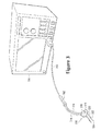
- FIGURE 3 is a perspective view of an oscilloscope.
- FIGURE 4 is a perspective sectional view of a resistor tip clip assembly attached to a device under test by alternative embodiments of the self-retaining via probes constructed in accordance with the principles of the present invention.
- FIGURE 5 is a close-up sectional view of a via anchor of the self-retaining via probe inserted into a via.
- FIGURE 6A is a close-up sectional view of a via anchor of the self-retaining via probe that has flexed in an arc during insertion.
- FIGURE 6B is a close-up sectional view of a via anchor of the self-retaining via probe that has flexed in a sinusoid shape during insertion.
- FIGURE 7 is a perspective exploded view of a tool for inserting a via anchor of the self-retaining via probe into a via.
- a preferred embodiment of the self-retaining via probe of the present invention is shown and generally designated by the reference numeral 10.
- FIGURE 1 illustrates a perspective view of a logic analyzer 200. More particularly, the logic analyzer 200 is connected to a waystation 212 by a ribbonized coaxial cable 210. Individual coaxial cable strands 216 emerge from the waystation and each terminate in a podlet 214. Each of the podlets 214 has an opening 216 that receives a self-retaining via probe 10.
- FIGURE 2 illustrates a perspective sectional view of a podlet 214 of FIGURE 1 attached to a Device Under Test (DUT) 100 by self-retaining via probes 10 (a signal via probe 38 and a ground via probe 40). More particularly, the podlet contains, on one side, the end of a coaxial cable strand 216 leading back to the waystation 212 of FIGURE 1 and subsequently to the logic analyzer 200. Within the podlet, the center conductor 220 of the coaxial cable strand attaches to a metal contact 222. The metal contact in turn makes a non-permanent, snap-on contact with the probe tip 34 of the backend 30 of the signal via probe 38. This contact exists so that the probe tip can be easily replaced to provide user options and repair capabilities.
- DUT Device Under Test
- the serve 218 (also sometimes referred to as the braid), which provides a grounding shield to the coaxial cable strand, is terminated to a ground solder strap 224.
- This strap also interfaces via a non-permanent, snap-on contact with the probe tip 36 of the backend 32 of the ground via probe 40, which is attached to the DUT's ground.
- Both the signal via probe 38 and the ground via probe 40 include a via anchor 48, which enables the self-retaining via probes 10 to engage and retain themselves within the vias 114 of the DUT 100.
- the signal via probe 38 includes a pad 26 in close proximity to the via anchor's base 14. The pad enables attachment of a passive isolation network 28.
- the passive isolation network is positioned in series. The passive isolation network serves to isolate the load of the self-retaining via probe from the DUT.
- the passive isolation network consists of a chip resistor and an optional capacitor in parallel with the resistor for better high frequency response.
- backends 30 and 32 provide a flexible means of attaching to a nearby ground. While many logic analyzer probes rely on tips that require a fixed spacing between the ground and signal pad, it is sometimes difficult to find a ground at this fixed distance.
- the backends can be bent to enable the ground via probe 40 to address any of the ground vias located adjacent to the area being probed by the signal via probe 38.
- FIGURE 3 illustrates a perspective view of an oscilloscope 300. More particularly, the oscilloscope 300 is connected to a differential probe 312 by a cable 310. Two cables 314 emerge from the differential probe and terminate in a probe lead 318. A resistor tip clip assembly 316 is detachably connected to the probe lead by a connector 326. Two cables 320 extend from the connector. Each of the cables 320 is attached to a resistor 322 with a wire segment 324.
- FIGURE 4 illustrates a perspective view of a tip clip assembly 316 of FIGURE 3 attached to a Device Under Test (DUT) 100 by self-retaining via probes 400 (a signal via probe 438 and a ground via probe 440, which is attached to the DUT's ground). More particularly, both the signal via probe and the ground via probe include a via anchor 48, which enables the self-retaining via probes 400 to engage and retain themselves within the vias 114 of the DUT 100. Both the signal via probe and the ground via probe also include a pad 26 in close proximity to the bases 14 of their via anchors.
- DUT Device Under Test
- the wire segments 324 of the tip clip assembly are attached to the pads 26 to create an electrical connection between the cables 320 leading back to the probe lead 318 of FIGURE 3 and subsequently to the oscilloscope 300.
- the wire segments are soldered to the pads to create a semi-permanent contact between the wire segments and pads.
- the wire segments can be un-soldered from the signal via probe and the ground via probe so that the signal via probe and the ground via probe can be easily replaced to provide options and repair capabilities to a user.
- cables 320 provide a flexible means of attaching to a nearby ground.
- the backends 430 and 436 of the signal via probe 438 and ground via probe 440 are truncated compared to the backends 30 and 36 of the signal via probe 38 and ground via probe 40. While many oscilloscope probes rely on tips that require a fixed spacing between the ground and signal pad, it is sometimes difficult to find a ground at this fixed distance.
- the cables 320 can be bent to enable the ground via probe 440 to address any of the ground vias located adjacent to the area being probed by the signal via probe 438.
- FIGURE 5 illustrates a close-up sectional view of a via anchor 48 inserted into a via 114.
- the via anchor is a planar body with a tapered, arrowhead-like tip 12 for easy insertion through a via.
- Barbs 16 located behind the tip resist backing out by engaging with the bottom face 112 of the DUT once the via anchor is fully inserted and the tip pokes through the DUT 100.
- Barbs 18 and 20 on the edges 24 of the via anchor terminate in sharp points that engage the sidewall 116 of the via to create point electrical contacts.
- Physical stops 22 at the base 14 of the anchor prevent the via anchor from being inserted too far into the via and provides tactile feedback to the user that the via anchor is fully inserted.
- FIGURE 6A illustrates a close-up sectional view of a via anchor 48 that has flexed in an arc during insertion.
- FIGURE 6B illustrates a close-up sectional view of a via anchor that has flexed in a sinusoid shape during insertion. More particularly, the via anchor material flexes either in an arc (the via anchor bends slightly during insertion into the via, with the front 44 becoming concave and the back 46 becoming convex) or a sinusoid shape (a result of the via anchor being twisted into the via). The subsequent flexing of the via anchor material after insertion forces the barbs 18 and 20 (only barbs 18 are visible) against the side wall of the via. In either configuration, the barbs contact the side walls with a force sufficient to establish a secure and reliable electrical connection between the via anchor and the via sidewall.
- the via anchor is not intended to damage or destroy the DUT.
- the thin sheet metal of the via anchor only provides enough force to engage the via sidewall's copper plating 118 electrically. The contact force is too low to break through the surface finish to the copper plating during insertion or use of the self-retaining via probe 10.
- the via anchors are removable from the vias, but the anchors are unlikely to be reusable because of the amount of deformation of the barbs 16 required to permit passage of the tip 12 back through the via.
- a low-cost process of manufacture makes the self-retaining via probes 10 economically feasible to be viewed as a consumable item.
- FIGURE 7 illustrates a perspective exploded view of a tool 300 for inserting a via anchor 48 into a via 114. More particularly, the tool assists in inserting the via anchor into the via and prevents tip buckling of the via anchor.
- This insertion tool slightly deforms the via anchor (within the elastic limits of the via anchor) to provide a cross-section that will endure the buckling insertion forces as the via anchor is inserted into a via.
- the tool has a core side 312 and a cavity side 310.
- the cavity side has two hubs 314 that locate the via anchor within the cavity side by contacting locations 42 on the stops 22.
- the core side 312 and cavity side 310 are then pinched together to squeeze and slightly flex the via anchor into the arc shown in FIGURE 6A .
- an alternative embodiment of the via anchors would not fully insert through a via and hook to the opposite side to resist removal. Instead, the alternative embodiment would rely on friction forces against the via sidewall for retention. This would be helpful in the cases of blind vias that do not fully pass through all layers of the Device Under Test and vias that have components mounted on their opposite end. While the retention of the alternative embodiment of the via anchors would not necessarily be as high as that of the current invention, it would still provide enough force to keep the via anchors in place during a test.
Landscapes
- Physics & Mathematics (AREA)
- Geometry (AREA)
- General Physics & Mathematics (AREA)
- Measuring Leads Or Probes (AREA)
Abstract
Description
- The present invention relates to logic analyzer and oscilloscope probes, and more particularly to probing devices under test.
- A secure and reliable method of probing many different signals simultaneously and feeding them back to a logic analyzer or oscilloscope is required to acquire the desired data from a Device Under Test (DUT). Conventionally, there are two options for probing in this way. The first option is to design into the DUT, a logic analyzer or oscilloscope connector or land pattern, at a specific location. This connector or land pattern interfaces with a logic analyzer or oscilloscope probe. This can be problematic if the traces must detour from their natural path to this location, because such a detour adds signal loss to the circuit being tested. This approach also reduces the flexibility of the layout design and occupies valuable circuit board space.
- The second option is to attach the logic analyzer or oscilloscope probes to existing component leads. However, newer and emerging circuit board technologies, such as surface mount components and ball-grid-array components, reduce the number of available leads to which a logic analyzer or oscilloscope probe may be attached. These technologies can even "hide" all potential test points completely, making it impossible to attach the logic analyzer or oscilloscope probes anywhere on the circuit board.
- For applications where a convenient test point is accessible, a third option most commonly applied to oscilloscopes is the original hand-held probe. This method keeps a user's hand occupied during probing and relies on an individual's manual dexterity to keep the probe placed in the right location while visual attention is focused on data from the oscilloscope. Because of the human intervention in this process, the connection is not as secure and reliable as it could be.
- When none of the conventional options can be utilized, one of the few remaining options for probing a test point is to attach a logic analyzer or oscilloscope probe to vias in the DUT. However, vias are small features, which makes it difficult to retain a logic analyzer probe within a via during a test. A via is a vertical electrical connection between different layers of conductors in a printed circuit board. It consists of two or more pads, in corresponding positions on different layers of the board, which are electrically connected by a cylindrical hole drilled through the board. The hole is made conductive by electroplating, or is lined with a conductive tube or a rivet.
- Therefore, there is a need for a probe that retains itself in a via of a Device Under Test (DUT).
- The present invention provides an improved self-retaining via probe, and overcomes the above-mentioned disadvantages and drawbacks of the prior art. As such, the general purpose of the present invention, which will be described subsequently in greater detail, is to provide an improved self-retaining via probe that has all the advantages of the prior art mentioned above.
- To attain this, the preferred embodiment of the present invention essentially comprises a planar body that is configured such that its edges engage the sidewall of a via of a device under test to create electrical contacts and the planar body resists removal of the planar body from the via after insertion. The edges of the planar body may include barbs that resist removal of the planar body from the via after insertion. These barbs may engage the sidewall of the via to create point electrical contacts or engage a face of the device under test to resist the removal of the planar body. The end of the body that is inserted into the via may form a tapered tip to facilitate insertion. The end of the planar body that is inserted into the via may include barbs that resist removal of the planar body from the via after insertion. The edges of the planar body may include stops that prevent further insertion of the planar body into the via beyond the stops. There are, of course, additional features of the invention that will be described hereinafter and which will form the subject matter of the claims attached.
- There has thus been outlined, rather broadly, the more important features of the invention in order that the detailed description thereof that follows may be better understood and in order that the present contribution to the art may be better appreciated.
-
FIGURE 1 is a perspective view of a logic analyzer. -
FIGURE 2 is a perspective sectional view of a podlet attached to a device under test by self-retaining via probes constructed in accordance with the principles of the present invention. -
FIGURE 3 is a perspective view of an oscilloscope. -
FIGURE 4 is a perspective sectional view of a resistor tip clip assembly attached to a device under test by alternative embodiments of the self-retaining via probes constructed in accordance with the principles of the present invention. -
FIGURE 5 is a close-up sectional view of a via anchor of the self-retaining via probe inserted into a via. -
FIGURE 6A is a close-up sectional view of a via anchor of the self-retaining via probe that has flexed in an arc during insertion. -
FIGURE 6B is a close-up sectional view of a via anchor of the self-retaining via probe that has flexed in a sinusoid shape during insertion. -
FIGURE 7 is a perspective exploded view of a tool for inserting a via anchor of the self-retaining via probe into a via. - The same reference numerals refer to the same parts throughout the various figures.
- A preferred embodiment of the self-retaining via probe of the present invention is shown and generally designated by the
reference numeral 10. -
FIGURE 1 illustrates a perspective view of alogic analyzer 200. More particularly, thelogic analyzer 200 is connected to awaystation 212 by a ribbonizedcoaxial cable 210. Individualcoaxial cable strands 216 emerge from the waystation and each terminate in apodlet 214. Each of thepodlets 214 has anopening 216 that receives a self-retaining viaprobe 10. -
FIGURE 2 illustrates a perspective sectional view of apodlet 214 ofFIGURE 1 attached to a Device Under Test (DUT) 100 by self-retaining via probes 10 (a signal viaprobe 38 and a ground via probe 40). More particularly, the podlet contains, on one side, the end of acoaxial cable strand 216 leading back to thewaystation 212 ofFIGURE 1 and subsequently to thelogic analyzer 200. Within the podlet, thecenter conductor 220 of the coaxial cable strand attaches to ametal contact 222. The metal contact in turn makes a non-permanent, snap-on contact with theprobe tip 34 of thebackend 30 of the signal viaprobe 38. This contact exists so that the probe tip can be easily replaced to provide user options and repair capabilities. The serve 218 (also sometimes referred to as the braid), which provides a grounding shield to the coaxial cable strand, is terminated to aground solder strap 224. This strap also interfaces via a non-permanent, snap-on contact with theprobe tip 36 of thebackend 32 of the ground viaprobe 40, which is attached to the DUT's ground. - Both the signal via
probe 38 and the ground viaprobe 40 include avia anchor 48, which enables the self-retaining viaprobes 10 to engage and retain themselves within thevias 114 of theDUT 100. The signal viaprobe 38 includes apad 26 in close proximity to the via anchor'sbase 14. The pad enables attachment of apassive isolation network 28. The passive isolation network is positioned in series. The passive isolation network serves to isolate the load of the self-retaining via probe from the DUT. Typically, the passive isolation network consists of a chip resistor and an optional capacitor in parallel with the resistor for better high frequency response. - An advantage of the
backends probe 40 to address any of the ground vias located adjacent to the area being probed by the signal viaprobe 38. -
FIGURE 3 illustrates a perspective view of anoscilloscope 300. More particularly, theoscilloscope 300 is connected to adifferential probe 312 by acable 310. Twocables 314 emerge from the differential probe and terminate in aprobe lead 318. A resistortip clip assembly 316 is detachably connected to the probe lead by aconnector 326. Twocables 320 extend from the connector. Each of thecables 320 is attached to aresistor 322 with awire segment 324. -
FIGURE 4 illustrates a perspective view of atip clip assembly 316 ofFIGURE 3 attached to a Device Under Test (DUT) 100 by self-retaining via probes 400 (a signal viaprobe 438 and a ground viaprobe 440, which is attached to the DUT's ground). More particularly, both the signal via probe and the ground via probe include a viaanchor 48, which enables the self-retaining viaprobes 400 to engage and retain themselves within thevias 114 of theDUT 100. Both the signal via probe and the ground via probe also include apad 26 in close proximity to thebases 14 of their via anchors. Thewire segments 324 of the tip clip assembly are attached to thepads 26 to create an electrical connection between thecables 320 leading back to theprobe lead 318 ofFIGURE 3 and subsequently to theoscilloscope 300. In the current embodiment, the wire segments are soldered to the pads to create a semi-permanent contact between the wire segments and pads. However, the wire segments can be un-soldered from the signal via probe and the ground via probe so that the signal via probe and the ground via probe can be easily replaced to provide options and repair capabilities to a user. - An advantage of the
cables 320 is that they provide a flexible means of attaching to a nearby ground. As a result, thebackends probe 438 and ground viaprobe 440 are truncated compared to thebackends probe 38 and ground viaprobe 40. While many oscilloscope probes rely on tips that require a fixed spacing between the ground and signal pad, it is sometimes difficult to find a ground at this fixed distance. Thecables 320 can be bent to enable the ground viaprobe 440 to address any of the ground vias located adjacent to the area being probed by the signal viaprobe 438. -
FIGURE 5 illustrates a close-up sectional view of a viaanchor 48 inserted into a via 114. More particularly, the via anchor is a planar body with a tapered, arrowhead-like tip 12 for easy insertion through a via.Barbs 16 located behind the tip resist backing out by engaging with thebottom face 112 of the DUT once the via anchor is fully inserted and the tip pokes through theDUT 100.Barbs edges 24 of the via anchor terminate in sharp points that engage thesidewall 116 of the via to create point electrical contacts. Physical stops 22 at thebase 14 of the anchor prevent the via anchor from being inserted too far into the via and provides tactile feedback to the user that the via anchor is fully inserted. -
FIGURE 6A illustrates a close-up sectional view of a viaanchor 48 that has flexed in an arc during insertion.FIGURE 6B illustrates a close-up sectional view of a via anchor that has flexed in a sinusoid shape during insertion. More particularly, the via anchor material flexes either in an arc (the via anchor bends slightly during insertion into the via, with the front 44 becoming concave and the back 46 becoming convex) or a sinusoid shape (a result of the via anchor being twisted into the via). The subsequent flexing of the via anchor material after insertion forces thebarbs 18 and 20 (onlybarbs 18 are visible) against the side wall of the via. In either configuration, the barbs contact the side walls with a force sufficient to establish a secure and reliable electrical connection between the via anchor and the via sidewall. - However, the via anchor is not intended to damage or destroy the DUT. The thin sheet metal of the via anchor only provides enough force to engage the via sidewall's copper plating 118 electrically. The contact force is too low to break through the surface finish to the copper plating during insertion or use of the self-retaining via
probe 10. - The via anchors are removable from the vias, but the anchors are unlikely to be reusable because of the amount of deformation of the
barbs 16 required to permit passage of thetip 12 back through the via. However, a low-cost process of manufacture makes the self-retaining viaprobes 10 economically feasible to be viewed as a consumable item. -
FIGURE 7 illustrates a perspective exploded view of atool 300 for inserting a viaanchor 48 into a via 114. More particularly, the tool assists in inserting the via anchor into the via and prevents tip buckling of the via anchor. This insertion tool slightly deforms the via anchor (within the elastic limits of the via anchor) to provide a cross-section that will endure the buckling insertion forces as the via anchor is inserted into a via. The tool has acore side 312 and acavity side 310. The cavity side has twohubs 314 that locate the via anchor within the cavity side by contactinglocations 42 on thestops 22. Thecore side 312 andcavity side 310 are then pinched together to squeeze and slightly flex the via anchor into the arc shown inFIGURE 6A . - While current embodiments of the self-retaining via probe have been described in detail, it should be apparent that modifications and variations thereto are possible, all of which fall within the true spirit and scope of the invention. With respect to the above description then, it is to be realized that the optimum dimensional relationships for the parts of the invention, to include variations in size, materials, shape, form, function and manner of operation, assembly and use, are deemed readily apparent and obvious to one skilled in the art, and all equivalent relationships to those illustrated in the drawings and described in the specification are intended to be encompassed by the present invention. For example, different via anchor sizes could be made available to accommodate the assortment of via lengths and diameters found in industry.
- Finally, while the illustrations show the via anchors of the current invention fully inserted through a circuit board, an alternative embodiment of the via anchors would not fully insert through a via and hook to the opposite side to resist removal. Instead, the alternative embodiment would rely on friction forces against the via sidewall for retention. This would be helpful in the cases of blind vias that do not fully pass through all layers of the Device Under Test and vias that have components mounted on their opposite end. While the retention of the alternative embodiment of the via anchors would not necessarily be as high as that of the current invention, it would still provide enough force to keep the via anchors in place during a test.
- Therefore, the foregoing is considered as illustrative only of the principles of the invention. Further, since numerous modifications and changes will readily occur to those skilled in the art, it is not desired to limit the invention to the exact construction and operation shown and described, and accordingly, all suitable modifications and equivalents may be resorted to, falling within the scope of the invention.
Claims (15)
- A probe for insertion into a via of a device under test, the probe comprising:a planar body having opposed edges and opposed ends;the planar body being configured such that the edges engage a sidewall of a via of a device under test to create electrical contacts when one end of said opposed ends is inserted into the via; andwherein the planar body is configured to resist the removal of the planar body from the via after insertion.
- The probe of claim 1, wherein the edges of the planar body comprise a plurality of barbs that engage the sidewall of the via to create point electrical contacts and resist the removal of the planar body from the via after insertion.
- The probe of claim 1 or 2, wherein said one end for insertion into a via has a tapered tip to facilitate insertion.
- The probe of any preceding claim, wherein said one end for insertion into a via comprises a plurality of barbs that extend outward from the edges of the planar body more than a diameter of the via and engage with a face of the device under test to resist the removal of the planar body from the via after insertion.
- The probe of any preceding claim, wherein the edges of the planar body comprise a plurality of stops that extend outward from the edges of the planar body more than a diameter of the via and engage with a face of the device under test to prevent further insertion of the planar body into the via beyond the stops.
- The probe of any preceding claim, wherein the other end of the opposed ends of the planar body, that is not inserted into a via, terminates in a non-permanent contact configured to create an electrical connection with a cable to transmit electrical signals from the via to the cable.
- The probe of any preceding claim, wherein the planar body comprises a pad configured to attach to one of the group consisting of a passive isolation network and an oscilloscope probe.
- The probe of any preceding claim, wherein the planar body is flexible into an arc prior to being inserted into the via.
- The probe of claim 8, wherein the planar body is flexible into an arc prior to being inserted into the via by a tool.
- The probe of any preceding claim, wherein the planar body is flexible into a sinusoidal shape by being twisted during insertion into the via.
- A logic analysis system comprising:a logic analyzer;a cable having one end connected to the logic analyzer;an opposing end of the cable connected to a waystation;the waystation separating the cable into a plurality of cable strands;each of the cable strands being connected to a podlet;each of the podlets creating a non-permanent electrical connection between a cable strand and a signal via probe and a ground via probe;the signal via probe and the ground via probe each comprising a probe as claimed in any preceding claim.
- The system of claim 11, wherein the signal via probe and the ground via probe are flexible, such that the spacing between the signal via probe in the ground via probe is adjustable.
- A signal probing system comprising:an oscilloscope;a cable having one end connected to the oscilloscope;an opposing end of the cable connected to a differential probe;the differential probe separating the cable into a plurality of cables;the cables being connected to a probe lead;the probe lead being connected to a resistor tip clip assembly;each of the resistor tip clip assemblies creating a semi-permanent electrical connection between the probe lead and a signal via probe and a ground via probe;the signal via probe and the ground via probe each comprising a probe as claimed in any of claims 1 to 10.
- The system of claim 13, wherein the signal via probe and the ground via probe are flexible, such that the spacing between the signal via probe in the ground via probe is adjustable.
- The system of claim 13 or 14, wherein the resistor tip clip assembly comprises a plurality of cables connected to resistors having wire segments having a free end, and wherein the planar body of the via anchor of the signal via probe and the planar body of the via anchor of the ground via probe each comprise a pad configured to attach to the free end of a wire segment of the resistor tip clip assembly.
Applications Claiming Priority (1)
| Application Number | Priority Date | Filing Date | Title |
|---|---|---|---|
| US13/197,662 US9007083B2 (en) | 2011-08-03 | 2011-08-03 | Self-retaining via probe |
Publications (3)
| Publication Number | Publication Date |
|---|---|
| EP2555002A2 true EP2555002A2 (en) | 2013-02-06 |
| EP2555002A3 EP2555002A3 (en) | 2014-11-26 |
| EP2555002B1 EP2555002B1 (en) | 2016-09-14 |
Family
ID=47074572
Family Applications (1)
| Application Number | Title | Priority Date | Filing Date |
|---|---|---|---|
| EP12176965.7A Not-in-force EP2555002B1 (en) | 2011-08-03 | 2012-07-18 | Self-retaining via probe |
Country Status (4)
| Country | Link |
|---|---|
| US (1) | US9007083B2 (en) |
| EP (1) | EP2555002B1 (en) |
| JP (1) | JP6359794B2 (en) |
| CN (2) | CN102914672A (en) |
Families Citing this family (4)
| Publication number | Priority date | Publication date | Assignee | Title |
|---|---|---|---|---|
| US10228390B2 (en) * | 2015-08-11 | 2019-03-12 | Tektronix, Inc. | Cable assembly with spine for instrument probe |
| KR102653198B1 (en) * | 2016-10-18 | 2024-04-01 | 삼성전기주식회사 | Unit for measuring electrical characteristics |
| US10845384B2 (en) * | 2017-11-07 | 2020-11-24 | Tektronix. Inc. | Surface-mountable apparatus for coupling a test and measurement instrument to a device under test |
| IT201800007898A1 (en) * | 2018-08-06 | 2020-02-06 | Technoprobe Spa | Contact probe with improved performance and related measuring head |
Family Cites Families (16)
| Publication number | Priority date | Publication date | Assignee | Title |
|---|---|---|---|---|
| US2015421A (en) * | 1931-12-02 | 1935-09-24 | Deal Electric Co Inc | Attachment plug |
| JPH05121142A (en) * | 1991-10-31 | 1993-05-18 | Yazaki Corp | Board terminal manufacturing method |
| US5223787A (en) | 1992-05-29 | 1993-06-29 | Tektronix, Inc. | High-speed, low-profile test probe |
| DE19529509A1 (en) | 1995-08-10 | 1997-02-13 | Heinzinger Electronic Gmbh | Power supply arrangement and method for controlling and regulating the same |
| JP3024946U (en) * | 1995-08-24 | 1996-06-07 | モレックス インコーポレーテッド | Electrical connector terminal |
| JPH09229964A (en) * | 1996-02-20 | 1997-09-05 | Hitachi Electron Eng Co Ltd | Through-hole probe |
| US5879168A (en) * | 1997-05-29 | 1999-03-09 | International Business Machines Corporation | Single C-beam contact |
| US5957222A (en) * | 1997-06-10 | 1999-09-28 | Charles T. Webb | Directional drilling system |
| CN1224258A (en) * | 1997-12-10 | 1999-07-28 | 特克特朗尼克公司 | Dual contact banana connector |
| US6222378B1 (en) | 1999-05-28 | 2001-04-24 | Tektronix, Inc. | Probe adapter for a ball-grid-array package |
| US7247050B1 (en) | 2006-10-24 | 2007-07-24 | Fci Americas Technology, Inc. | Press-fit electrical contact |
| WO2008093175A1 (en) * | 2007-02-02 | 2008-08-07 | Fci | Connection device |
| US7592822B2 (en) | 2007-12-17 | 2009-09-22 | Tektronix, Inc. | Probing adapter for a signal acquisition probe having pivoting, compliant, variable spacing probing tips |
| EP2091106B1 (en) * | 2008-01-17 | 2013-10-02 | Denso Corporation | Retaining member, electric component and electric device |
| US20090302874A1 (en) | 2008-06-06 | 2009-12-10 | International Business Machines Corporation | Method and apparatus for signal probe contact with circuit board vias |
| US20100073018A1 (en) * | 2008-09-23 | 2010-03-25 | Tektronix, Inc. | Adjustable probe head |
-
2011
- 2011-08-03 US US13/197,662 patent/US9007083B2/en not_active Expired - Fee Related
-
2012
- 2012-07-18 EP EP12176965.7A patent/EP2555002B1/en not_active Not-in-force
- 2012-08-03 CN CN2012102748215A patent/CN102914672A/en active Pending
- 2012-08-03 CN CN201811562985.1A patent/CN110058062A/en not_active Withdrawn
- 2012-08-03 JP JP2012172993A patent/JP6359794B2/en not_active Expired - Fee Related
Non-Patent Citations (1)
| Title |
|---|
| None |
Also Published As
| Publication number | Publication date |
|---|---|
| CN110058062A (en) | 2019-07-26 |
| EP2555002A3 (en) | 2014-11-26 |
| US20130033280A1 (en) | 2013-02-07 |
| EP2555002B1 (en) | 2016-09-14 |
| JP2013036997A (en) | 2013-02-21 |
| US9007083B2 (en) | 2015-04-14 |
| CN102914672A (en) | 2013-02-06 |
| JP6359794B2 (en) | 2018-07-18 |
Similar Documents
| Publication | Publication Date | Title |
|---|---|---|
| US6863576B2 (en) | Electrical test probe flexible spring tip | |
| US20050037649A1 (en) | Electronic probe extender | |
| US9007083B2 (en) | Self-retaining via probe | |
| US6417684B1 (en) | Securement of test points in a test head | |
| EP0563234B1 (en) | Testing clip and circuit board contacting method | |
| WO2002010784A1 (en) | Notched electrical test probe tip | |
| JP2002116222A (en) | Variable spacing probe tip adapter for differential measurement probes | |
| JP2019138768A (en) | probe | |
| JP4660616B2 (en) | Board inspection equipment | |
| CN104977440A (en) | Test probe and method of manufacturing a test probe | |
| WO2002010780A1 (en) | Electrical test probe wedge tip | |
| EP2746781B1 (en) | High bandwidth differential lead with device connection | |
| CN109041415A (en) | Circuit board, the production method of circuit board, debugging circuit board device and electronic equipment | |
| CN110389241B (en) | Probe holder and its rectangular probe | |
| US8336190B2 (en) | Method of calibrating a test instrument | |
| WO2018067810A1 (en) | Electrical connector for unterminated cables | |
| EP2866037A1 (en) | Releaseable probe connection | |
| US20090302874A1 (en) | Method and apparatus for signal probe contact with circuit board vias | |
| CN206832861U (en) | Test probe and printed circuit board test fixture | |
| JPH09229964A (en) | Through-hole probe | |
| CN113252264A (en) | Test tool | |
| EP3051296A1 (en) | Magnetic anchor for test probes with metal bands | |
| US7977960B2 (en) | Cantilever type probe head having introducing portion with end face having a tapered portion and an extended rectangular portion | |
| EP4579252A1 (en) | Circuit board test terminal | |
| KR200300719Y1 (en) | Terminal union structure for measuring instrument |
Legal Events
| Date | Code | Title | Description |
|---|---|---|---|
| PUAI | Public reference made under article 153(3) epc to a published international application that has entered the european phase |
Free format text: ORIGINAL CODE: 0009012 |
|
| AK | Designated contracting states |
Kind code of ref document: A2 Designated state(s): AL AT BE BG CH CY CZ DE DK EE ES FI FR GB GR HR HU IE IS IT LI LT LU LV MC MK MT NL NO PL PT RO RS SE SI SK SM TR |
|
| AX | Request for extension of the european patent |
Extension state: BA ME |
|
| RAP1 | Party data changed (applicant data changed or rights of an application transferred) |
Owner name: TEKTRONIX, INC. |
|
| PUAL | Search report despatched |
Free format text: ORIGINAL CODE: 0009013 |
|
| AK | Designated contracting states |
Kind code of ref document: A3 Designated state(s): AL AT BE BG CH CY CZ DE DK EE ES FI FR GB GR HR HU IE IS IT LI LT LU LV MC MK MT NL NO PL PT RO RS SE SI SK SM TR |
|
| AX | Request for extension of the european patent |
Extension state: BA ME |
|
| RIC1 | Information provided on ipc code assigned before grant |
Ipc: G01R 1/067 20060101AFI20141022BHEP |
|
| 17P | Request for examination filed |
Effective date: 20150519 |
|
| RBV | Designated contracting states (corrected) |
Designated state(s): AL AT BE BG CH CY CZ DE DK EE ES FI FR GB GR HR HU IE IS IT LI LT LU LV MC MK MT NL NO PL PT RO RS SE SI SK SM TR |
|
| GRAP | Despatch of communication of intention to grant a patent |
Free format text: ORIGINAL CODE: EPIDOSNIGR1 |
|
| INTG | Intention to grant announced |
Effective date: 20160210 |
|
| GRAS | Grant fee paid |
Free format text: ORIGINAL CODE: EPIDOSNIGR3 |
|
| GRAA | (expected) grant |
Free format text: ORIGINAL CODE: 0009210 |
|
| AK | Designated contracting states |
Kind code of ref document: B1 Designated state(s): AL AT BE BG CH CY CZ DE DK EE ES FI FR GB GR HR HU IE IS IT LI LT LU LV MC MK MT NL NO PL PT RO RS SE SI SK SM TR |
|
| REG | Reference to a national code |
Ref country code: GB Ref legal event code: FG4D |
|
| REG | Reference to a national code |
Ref country code: CH Ref legal event code: EP |
|
| REG | Reference to a national code |
Ref country code: IE Ref legal event code: FG4D |
|
| REG | Reference to a national code |
Ref country code: AT Ref legal event code: REF Ref document number: 829567 Country of ref document: AT Kind code of ref document: T Effective date: 20161015 |
|
| REG | Reference to a national code |
Ref country code: DE Ref legal event code: R096 Ref document number: 602012022722 Country of ref document: DE |
|
| REG | Reference to a national code |
Ref country code: LT Ref legal event code: MG4D |
|
| REG | Reference to a national code |
Ref country code: NL Ref legal event code: MP Effective date: 20160914 |
|
| PG25 | Lapsed in a contracting state [announced via postgrant information from national office to epo] |
Ref country code: RS Free format text: LAPSE BECAUSE OF FAILURE TO SUBMIT A TRANSLATION OF THE DESCRIPTION OR TO PAY THE FEE WITHIN THE PRESCRIBED TIME-LIMIT Effective date: 20160914 Ref country code: NO Free format text: LAPSE BECAUSE OF FAILURE TO SUBMIT A TRANSLATION OF THE DESCRIPTION OR TO PAY THE FEE WITHIN THE PRESCRIBED TIME-LIMIT Effective date: 20161214 Ref country code: FI Free format text: LAPSE BECAUSE OF FAILURE TO SUBMIT A TRANSLATION OF THE DESCRIPTION OR TO PAY THE FEE WITHIN THE PRESCRIBED TIME-LIMIT Effective date: 20160914 Ref country code: LT Free format text: LAPSE BECAUSE OF FAILURE TO SUBMIT A TRANSLATION OF THE DESCRIPTION OR TO PAY THE FEE WITHIN THE PRESCRIBED TIME-LIMIT Effective date: 20160914 Ref country code: HR Free format text: LAPSE BECAUSE OF FAILURE TO SUBMIT A TRANSLATION OF THE DESCRIPTION OR TO PAY THE FEE WITHIN THE PRESCRIBED TIME-LIMIT Effective date: 20160914 |
|
| REG | Reference to a national code |
Ref country code: AT Ref legal event code: MK05 Ref document number: 829567 Country of ref document: AT Kind code of ref document: T Effective date: 20160914 |
|
| PG25 | Lapsed in a contracting state [announced via postgrant information from national office to epo] |
Ref country code: GR Free format text: LAPSE BECAUSE OF FAILURE TO SUBMIT A TRANSLATION OF THE DESCRIPTION OR TO PAY THE FEE WITHIN THE PRESCRIBED TIME-LIMIT Effective date: 20161215 Ref country code: LV Free format text: LAPSE BECAUSE OF FAILURE TO SUBMIT A TRANSLATION OF THE DESCRIPTION OR TO PAY THE FEE WITHIN THE PRESCRIBED TIME-LIMIT Effective date: 20160914 Ref country code: NL Free format text: LAPSE BECAUSE OF FAILURE TO SUBMIT A TRANSLATION OF THE DESCRIPTION OR TO PAY THE FEE WITHIN THE PRESCRIBED TIME-LIMIT Effective date: 20160914 Ref country code: SE Free format text: LAPSE BECAUSE OF FAILURE TO SUBMIT A TRANSLATION OF THE DESCRIPTION OR TO PAY THE FEE WITHIN THE PRESCRIBED TIME-LIMIT Effective date: 20160914 |
|
| PG25 | Lapsed in a contracting state [announced via postgrant information from national office to epo] |
Ref country code: EE Free format text: LAPSE BECAUSE OF FAILURE TO SUBMIT A TRANSLATION OF THE DESCRIPTION OR TO PAY THE FEE WITHIN THE PRESCRIBED TIME-LIMIT Effective date: 20160914 Ref country code: RO Free format text: LAPSE BECAUSE OF FAILURE TO SUBMIT A TRANSLATION OF THE DESCRIPTION OR TO PAY THE FEE WITHIN THE PRESCRIBED TIME-LIMIT Effective date: 20160914 |
|
| PG25 | Lapsed in a contracting state [announced via postgrant information from national office to epo] |
Ref country code: AT Free format text: LAPSE BECAUSE OF FAILURE TO SUBMIT A TRANSLATION OF THE DESCRIPTION OR TO PAY THE FEE WITHIN THE PRESCRIBED TIME-LIMIT Effective date: 20160914 Ref country code: PT Free format text: LAPSE BECAUSE OF FAILURE TO SUBMIT A TRANSLATION OF THE DESCRIPTION OR TO PAY THE FEE WITHIN THE PRESCRIBED TIME-LIMIT Effective date: 20170116 Ref country code: IS Free format text: LAPSE BECAUSE OF FAILURE TO SUBMIT A TRANSLATION OF THE DESCRIPTION OR TO PAY THE FEE WITHIN THE PRESCRIBED TIME-LIMIT Effective date: 20170114 Ref country code: SK Free format text: LAPSE BECAUSE OF FAILURE TO SUBMIT A TRANSLATION OF THE DESCRIPTION OR TO PAY THE FEE WITHIN THE PRESCRIBED TIME-LIMIT Effective date: 20160914 Ref country code: CZ Free format text: LAPSE BECAUSE OF FAILURE TO SUBMIT A TRANSLATION OF THE DESCRIPTION OR TO PAY THE FEE WITHIN THE PRESCRIBED TIME-LIMIT Effective date: 20160914 Ref country code: PL Free format text: LAPSE BECAUSE OF FAILURE TO SUBMIT A TRANSLATION OF THE DESCRIPTION OR TO PAY THE FEE WITHIN THE PRESCRIBED TIME-LIMIT Effective date: 20160914 Ref country code: SM Free format text: LAPSE BECAUSE OF FAILURE TO SUBMIT A TRANSLATION OF THE DESCRIPTION OR TO PAY THE FEE WITHIN THE PRESCRIBED TIME-LIMIT Effective date: 20160914 Ref country code: BE Free format text: LAPSE BECAUSE OF FAILURE TO SUBMIT A TRANSLATION OF THE DESCRIPTION OR TO PAY THE FEE WITHIN THE PRESCRIBED TIME-LIMIT Effective date: 20160914 Ref country code: BG Free format text: LAPSE BECAUSE OF FAILURE TO SUBMIT A TRANSLATION OF THE DESCRIPTION OR TO PAY THE FEE WITHIN THE PRESCRIBED TIME-LIMIT Effective date: 20161214 Ref country code: ES Free format text: LAPSE BECAUSE OF FAILURE TO SUBMIT A TRANSLATION OF THE DESCRIPTION OR TO PAY THE FEE WITHIN THE PRESCRIBED TIME-LIMIT Effective date: 20160914 |
|
| REG | Reference to a national code |
Ref country code: DE Ref legal event code: R097 Ref document number: 602012022722 Country of ref document: DE |
|
| PG25 | Lapsed in a contracting state [announced via postgrant information from national office to epo] |
Ref country code: IT Free format text: LAPSE BECAUSE OF FAILURE TO SUBMIT A TRANSLATION OF THE DESCRIPTION OR TO PAY THE FEE WITHIN THE PRESCRIBED TIME-LIMIT Effective date: 20160914 |
|
| PLBE | No opposition filed within time limit |
Free format text: ORIGINAL CODE: 0009261 |
|
| STAA | Information on the status of an ep patent application or granted ep patent |
Free format text: STATUS: NO OPPOSITION FILED WITHIN TIME LIMIT |
|
| PG25 | Lapsed in a contracting state [announced via postgrant information from national office to epo] |
Ref country code: DK Free format text: LAPSE BECAUSE OF FAILURE TO SUBMIT A TRANSLATION OF THE DESCRIPTION OR TO PAY THE FEE WITHIN THE PRESCRIBED TIME-LIMIT Effective date: 20160914 |
|
| 26N | No opposition filed |
Effective date: 20170615 |
|
| PG25 | Lapsed in a contracting state [announced via postgrant information from national office to epo] |
Ref country code: SI Free format text: LAPSE BECAUSE OF FAILURE TO SUBMIT A TRANSLATION OF THE DESCRIPTION OR TO PAY THE FEE WITHIN THE PRESCRIBED TIME-LIMIT Effective date: 20160914 |
|
| REG | Reference to a national code |
Ref country code: CH Ref legal event code: PL |
|
| REG | Reference to a national code |
Ref country code: IE Ref legal event code: MM4A |
|
| REG | Reference to a national code |
Ref country code: FR Ref legal event code: ST Effective date: 20180330 |
|
| PG25 | Lapsed in a contracting state [announced via postgrant information from national office to epo] |
Ref country code: CH Free format text: LAPSE BECAUSE OF NON-PAYMENT OF DUE FEES Effective date: 20170731 Ref country code: LI Free format text: LAPSE BECAUSE OF NON-PAYMENT OF DUE FEES Effective date: 20170731 Ref country code: IE Free format text: LAPSE BECAUSE OF NON-PAYMENT OF DUE FEES Effective date: 20170718 |
|
| PG25 | Lapsed in a contracting state [announced via postgrant information from national office to epo] |
Ref country code: FR Free format text: LAPSE BECAUSE OF NON-PAYMENT OF DUE FEES Effective date: 20170731 |
|
| PG25 | Lapsed in a contracting state [announced via postgrant information from national office to epo] |
Ref country code: LU Free format text: LAPSE BECAUSE OF NON-PAYMENT OF DUE FEES Effective date: 20170718 |
|
| PG25 | Lapsed in a contracting state [announced via postgrant information from national office to epo] |
Ref country code: MT Free format text: LAPSE BECAUSE OF NON-PAYMENT OF DUE FEES Effective date: 20170718 |
|
| PG25 | Lapsed in a contracting state [announced via postgrant information from national office to epo] |
Ref country code: AL Free format text: LAPSE BECAUSE OF FAILURE TO SUBMIT A TRANSLATION OF THE DESCRIPTION OR TO PAY THE FEE WITHIN THE PRESCRIBED TIME-LIMIT Effective date: 20160914 |
|
| PGFP | Annual fee paid to national office [announced via postgrant information from national office to epo] |
Ref country code: GB Payment date: 20180727 Year of fee payment: 7 |
|
| PG25 | Lapsed in a contracting state [announced via postgrant information from national office to epo] |
Ref country code: MC Free format text: LAPSE BECAUSE OF FAILURE TO SUBMIT A TRANSLATION OF THE DESCRIPTION OR TO PAY THE FEE WITHIN THE PRESCRIBED TIME-LIMIT Effective date: 20160914 Ref country code: HU Free format text: LAPSE BECAUSE OF FAILURE TO SUBMIT A TRANSLATION OF THE DESCRIPTION OR TO PAY THE FEE WITHIN THE PRESCRIBED TIME-LIMIT; INVALID AB INITIO Effective date: 20120718 |
|
| PG25 | Lapsed in a contracting state [announced via postgrant information from national office to epo] |
Ref country code: CY Free format text: LAPSE BECAUSE OF NON-PAYMENT OF DUE FEES Effective date: 20160914 |
|
| PGFP | Annual fee paid to national office [announced via postgrant information from national office to epo] |
Ref country code: DE Payment date: 20190729 Year of fee payment: 8 |
|
| PG25 | Lapsed in a contracting state [announced via postgrant information from national office to epo] |
Ref country code: MK Free format text: LAPSE BECAUSE OF FAILURE TO SUBMIT A TRANSLATION OF THE DESCRIPTION OR TO PAY THE FEE WITHIN THE PRESCRIBED TIME-LIMIT Effective date: 20160914 |
|
| GBPC | Gb: european patent ceased through non-payment of renewal fee |
Effective date: 20190718 |
|
| PG25 | Lapsed in a contracting state [announced via postgrant information from national office to epo] |
Ref country code: TR Free format text: LAPSE BECAUSE OF FAILURE TO SUBMIT A TRANSLATION OF THE DESCRIPTION OR TO PAY THE FEE WITHIN THE PRESCRIBED TIME-LIMIT Effective date: 20160914 |
|
| PG25 | Lapsed in a contracting state [announced via postgrant information from national office to epo] |
Ref country code: GB Free format text: LAPSE BECAUSE OF NON-PAYMENT OF DUE FEES Effective date: 20190718 |
|
| REG | Reference to a national code |
Ref country code: DE Ref legal event code: R119 Ref document number: 602012022722 Country of ref document: DE |
|
| PG25 | Lapsed in a contracting state [announced via postgrant information from national office to epo] |
Ref country code: DE Free format text: LAPSE BECAUSE OF NON-PAYMENT OF DUE FEES Effective date: 20210202 |