EP2554607A1 - Microstructured device and method of fabrication - Google Patents
Microstructured device and method of fabrication Download PDFInfo
- Publication number
- EP2554607A1 EP2554607A1 EP12178949A EP12178949A EP2554607A1 EP 2554607 A1 EP2554607 A1 EP 2554607A1 EP 12178949 A EP12178949 A EP 12178949A EP 12178949 A EP12178949 A EP 12178949A EP 2554607 A1 EP2554607 A1 EP 2554607A1
- Authority
- EP
- European Patent Office
- Prior art keywords
- layer
- embossed
- thin film
- film coating
- coating
- Prior art date
- Legal status (The legal status is an assumption and is not a legal conclusion. Google has not performed a legal analysis and makes no representation as to the accuracy of the status listed.)
- Granted
Links
Images



Classifications
-
- C—CHEMISTRY; METALLURGY
- C09—DYES; PAINTS; POLISHES; NATURAL RESINS; ADHESIVES; COMPOSITIONS NOT OTHERWISE PROVIDED FOR; APPLICATIONS OF MATERIALS NOT OTHERWISE PROVIDED FOR
- C09C—TREATMENT OF INORGANIC MATERIALS, OTHER THAN FIBROUS FILLERS, TO ENHANCE THEIR PIGMENTING OR FILLING PROPERTIES ; PREPARATION OF CARBON BLACK ; PREPARATION OF INORGANIC MATERIALS WHICH ARE NO SINGLE CHEMICAL COMPOUNDS AND WHICH ARE MAINLY USED AS PIGMENTS OR FILLERS
- C09C1/00—Treatment of specific inorganic materials other than fibrous fillers; Preparation of carbon black
- C09C1/0015—Pigments exhibiting interference colours, e.g. transparent platelets of appropriate thinness or flaky substrates, e.g. mica, bearing appropriate thin transparent coatings
-
- G—PHYSICS
- G03—PHOTOGRAPHY; CINEMATOGRAPHY; ANALOGOUS TECHNIQUES USING WAVES OTHER THAN OPTICAL WAVES; ELECTROGRAPHY; HOLOGRAPHY
- G03H—HOLOGRAPHIC PROCESSES OR APPARATUS
- G03H1/00—Holographic processes or apparatus using light, infrared or ultraviolet waves for obtaining holograms or for obtaining an image from them; Details peculiar thereto
- G03H1/02—Details of features involved during the holographic process; Replication of holograms without interference recording
- G03H1/024—Hologram nature or properties
- G03H1/0244—Surface relief holograms
-
- G—PHYSICS
- G03—PHOTOGRAPHY; CINEMATOGRAPHY; ANALOGOUS TECHNIQUES USING WAVES OTHER THAN OPTICAL WAVES; ELECTROGRAPHY; HOLOGRAPHY
- G03H—HOLOGRAPHIC PROCESSES OR APPARATUS
- G03H1/00—Holographic processes or apparatus using light, infrared or ultraviolet waves for obtaining holograms or for obtaining an image from them; Details peculiar thereto
- G03H1/02—Details of features involved during the holographic process; Replication of holograms without interference recording
- G03H1/0272—Substrate bearing the hologram
-
- C—CHEMISTRY; METALLURGY
- C09—DYES; PAINTS; POLISHES; NATURAL RESINS; ADHESIVES; COMPOSITIONS NOT OTHERWISE PROVIDED FOR; APPLICATIONS OF MATERIALS NOT OTHERWISE PROVIDED FOR
- C09C—TREATMENT OF INORGANIC MATERIALS, OTHER THAN FIBROUS FILLERS, TO ENHANCE THEIR PIGMENTING OR FILLING PROPERTIES ; PREPARATION OF CARBON BLACK ; PREPARATION OF INORGANIC MATERIALS WHICH ARE NO SINGLE CHEMICAL COMPOUNDS AND WHICH ARE MAINLY USED AS PIGMENTS OR FILLERS
- C09C2210/00—Special effects or uses of interference pigments
- C09C2210/30—A layer or the substrate forming a grating
-
- C—CHEMISTRY; METALLURGY
- C09—DYES; PAINTS; POLISHES; NATURAL RESINS; ADHESIVES; COMPOSITIONS NOT OTHERWISE PROVIDED FOR; APPLICATIONS OF MATERIALS NOT OTHERWISE PROVIDED FOR
- C09C—TREATMENT OF INORGANIC MATERIALS, OTHER THAN FIBROUS FILLERS, TO ENHANCE THEIR PIGMENTING OR FILLING PROPERTIES ; PREPARATION OF CARBON BLACK ; PREPARATION OF INORGANIC MATERIALS WHICH ARE NO SINGLE CHEMICAL COMPOUNDS AND WHICH ARE MAINLY USED AS PIGMENTS OR FILLERS
- C09C2210/00—Special effects or uses of interference pigments
- C09C2210/40—Embossed layers
-
- G—PHYSICS
- G03—PHOTOGRAPHY; CINEMATOGRAPHY; ANALOGOUS TECHNIQUES USING WAVES OTHER THAN OPTICAL WAVES; ELECTROGRAPHY; HOLOGRAPHY
- G03H—HOLOGRAPHIC PROCESSES OR APPARATUS
- G03H1/00—Holographic processes or apparatus using light, infrared or ultraviolet waves for obtaining holograms or for obtaining an image from them; Details peculiar thereto
- G03H1/0005—Adaptation of holography to specific applications
- G03H1/0011—Adaptation of holography to specific applications for security or authentication
-
- G—PHYSICS
- G03—PHOTOGRAPHY; CINEMATOGRAPHY; ANALOGOUS TECHNIQUES USING WAVES OTHER THAN OPTICAL WAVES; ELECTROGRAPHY; HOLOGRAPHY
- G03H—HOLOGRAPHIC PROCESSES OR APPARATUS
- G03H1/00—Holographic processes or apparatus using light, infrared or ultraviolet waves for obtaining holograms or for obtaining an image from them; Details peculiar thereto
- G03H1/02—Details of features involved during the holographic process; Replication of holograms without interference recording
- G03H1/0276—Replicating a master hologram without interference recording
- G03H1/028—Replicating a master hologram without interference recording by embossing
-
- G—PHYSICS
- G03—PHOTOGRAPHY; CINEMATOGRAPHY; ANALOGOUS TECHNIQUES USING WAVES OTHER THAN OPTICAL WAVES; ELECTROGRAPHY; HOLOGRAPHY
- G03H—HOLOGRAPHIC PROCESSES OR APPARATUS
- G03H2270/00—Substrate bearing the hologram
- G03H2270/20—Shape
- G03H2270/24—Having particular size, e.g. microscopic
-
- Y—GENERAL TAGGING OF NEW TECHNOLOGICAL DEVELOPMENTS; GENERAL TAGGING OF CROSS-SECTIONAL TECHNOLOGIES SPANNING OVER SEVERAL SECTIONS OF THE IPC; TECHNICAL SUBJECTS COVERED BY FORMER USPC CROSS-REFERENCE ART COLLECTIONS [XRACs] AND DIGESTS
- Y10—TECHNICAL SUBJECTS COVERED BY FORMER USPC
- Y10T—TECHNICAL SUBJECTS COVERED BY FORMER US CLASSIFICATION
- Y10T428/00—Stock material or miscellaneous articles
- Y10T428/24—Structurally defined web or sheet [e.g., overall dimension, etc.]
- Y10T428/24802—Discontinuous or differential coating, impregnation or bond [e.g., artwork, printing, retouched photograph, etc.]
- Y10T428/24851—Intermediate layer is discontinuous or differential
Definitions
- This invention relates generally to a device having a microstructure such as a hologram, grating, grooves, alphanumeric symbol or other indicia formed therein and to the manufacture of thin film flakes having such microstructure.
- a microstructure such as a hologram, grating, grooves, alphanumeric symbol or other indicia formed therein and to the manufacture of thin film flakes having such microstructure.
- Thin film flakes such as color-shifting flakes have been manufactured for decades using what is now a standard process.
- a supporting web or substrate typically polyester terephthalate (PET) is coated with a thin film optical coating having a desired optical effect.
- PET polyester terephthalate
- a very thin release layer of soluble organic or inorganic material such as NaCl, wax, silicon or other suitable material is applied to the PET that allows the thin film optical coating coated thereover to be removed from the PET supporting layer.
- the thin film coating is released from the PET by passing it through a stripper containing solvent such as acetone or in some instances water, then over rollers and in a chamber containing solvent.
- the release layer In order to lessen the amount of solvent required to dissolve the release layer, and to reduce materials that have to be used in this process, it is desired to have the release layer be as thin as possible. In practice, the thickness of the release layer is many orders of magnitude thinner than the substrate it is coated on.
- the thin film optical coating is often applied by coating an absorber layer on top of the thin release layer in a vacuum chamber and subsequently coating a dielectric spacer layer over the absorber layer and then coating a reflective layer over the dielectric spacer layer.
- U.S. Patent 6,235,105 in the name of Hubbard discloses multilayer thin film materials produced by pre-coating a carrier substrate with a soluble release coating and depositing thin films of the optical materials in preselected sequence onto the carrier to build up the desired multilayer thin film structure, similar to the steps described above. Hubbard also discloses that alternatively, the substrate itself may be soluble. After deposition of the multilayer structure, the release coat (or the substrate) is dissolved, thereby freeing the multilayer structure from the substrate so that the same can be broken up into small flakes.
- Miekka in a similar manner as embossed thermoplastic layers are used today, utilizes a substrate of heat resistant polyethylene terephthalate (PET) base layer.
- PET polyethylene terephthalate
- the heat resistant PET is typically coated with a thermoplastic coating such as polyvinylchloride.
- An embossing pattern in holographic form can be formed on the thermoplastic layer which desirably contains a release agent such as hydroxylated polysiloxane which allows separation of the embossing from the embossing roller.
- Miekka further teaches as a first step of fabricating a grating or hologram, the provision of a heat resistant plastic film with a thermoplastic coating that has a softening temperature below the heat-distortion temperature of the heat resistant film.
- the thermoplastic is then heated to above its softening temperature and the softened thermoplastic layer is contacted with an embossing master.
- the contacting step involves the contact of the thermoplastic layer with an embossing master, which is an embossing roller, a metallic die, or a metalized plastic film, on the roller.
- the master can be used to form a homographic or diffractive pattern in the thermoplastic layer.
- thermoplastic surface is heated to above its softening temperature; and the softened thermoplastic surface is contacted with an embossing master at temperature below the thermoplastic softening temperature of the coating so that rapid embossing takes place and reflow of the plastic is avoided after separation of the coating.
- a separate thin release layer is coated over top of the embossed thermoplastic layer.
- the thin release layer can be NaCl, Na 2 B 4 O 7 hydrated (Borax) or another type of release layer is coated upon the stamped material which is subsequently coated in a vacuum chamber. Since the NaCl and borax are soluble in water, the coated product is then placed into a container of water and the coating is removed.
- Borax NaCl, Na 2 B 4 O 7 hydrated
- release layers such as NaCl or borax, left on the coating are harmful to one or more layers, for example to the absorber layer on color shifting flakes. Furthermore, it is desirous not to provide this thin release layer as its application includes an additional production step in manufacturing and extra materials being used.
- the typical process for producing thin-film flakes having microstructures therein has been to provide a substrate with a high softening temperature, coated or laminate with an embossing material having a lower softening temperature, then stamping the embossing material under suitable heat and pressure so as to form an embossing, and subsequently coating the embossed material with the thin release layer (NaCl or Borax) described above, followed by coating the release layer with the thin film coating.
- the next step involves submerging the coated structure in a bath of water and wiping the structure so as to release the flakes.
- this invention provides a solution that eliminates the addition of a release layer over the stamped embossed layer.
- a security device comprising:
- a thin film coating deposited directly upon the embossed layer, wherein the embossed layer is capable of being dissolved in a dissolving agent and wherein the thin film coating is not dissolvable by said dissolving agent.
- a security device comprising:
- a second layer having a microstructure embossed therein wherein the second layer is supported by and is in direct contact with the substrate and wherein the second layer has a softening temperature t2, wherein t2 ⁇ t1, wherein the second layer is a dissolvable layer that can be dissolved by a dissolving agent and wherein layer has a first thickness Th1 in cross-section in some regions and second thickness Th2 in other embossed regions, wherein Th2 ⁇ Th1; and, an optical coating including one or more layers coated directly upon the second layer, wherein at least one layer of the optical coating substantially conforms to the microstructure upon which it is coated, and wherein the optical coating provides an optical effect to light incident thereon, and wherein the optical coating is resistant to dissolving by the dissolving agent.
- a method of forming embossed thin film optical flakes comprising:
- dissolving the second layer with a dissolving agent so as to release the thin film coating from the second layer so as to form flakes, wherein the dissolving agent and is selected such that the optical coating is resistant to dissolving by the dissolving agent.
- Fig. 1 is a SEM micrograph of a cross section of a foil sample of Dunmore DUN-TRANTM, which has a base of PET with an embossable layer thereover and having a special layer of Cr coating for the purposes of enhancing the visibility of the interface applied for the purpose of increasing the contrast of portions of the SEM image;
- Fig. 2a is a plan view obtained by Atomic Force Microscopy of a portion of a stamped sheet of DUN-TRANTM stamped in a checkerboard pattern;
- Fig. 2b is an isometric view of the stamped sheet of Fig. 2a ;
- Fig. 2c is a chart showing varying height, hill width and valley width of the sample of Fig. 2b ;
- Fig. 3 is a black and white photo of the pigments obtained with the stamped foil obtained from the stamped sheet of DUN-TRANTM shown in Figs 2a and 2b ;
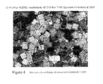
- Fig. 4 is shows stamped color shifting flakes made in accordance with this invention by embossing DUN-IRANTM film with framed squares having the logo JDSU and coating the stamped film with five layers of coating forming a color shifting coating thereon; the flakes shown display different colors at different observation angles;
- Fig. 5 is a cross-sectional view of a prior art DUN-TRANTM film.
- Fig. 5b is a special DUN-TRANTM film made with a thicker top embossing layer shown embossed and coated with three layers forming a color shift coating.
- This invention provides a security structure coated with one or more thin film layers that can be submerged in a bath of a solvent to provide microstructured thin film flakes directly from the deposited thin film layers.
- the flakes may be single layered flakes or can be multilayer microstructured flakes such as color shifting flakes useful in security applications wherein covert features are encoded into the flakes by way of an embossing of a carrier upon which the flake material is coaled.
- a thin release layer is not required between the coating layer and the embossed supporting layer.
- the embossed layer itself becomes the release layer, as it is dissolvable in a solvent which does not dissolve the thin film coating.
- the embossing layer would have to provide acceptable embossing characteristics, replicate the stamp within embossing shim accurately, have a softening temperature that was less than the supporting substrate; and be dissolvable in a solvent that would not dissolve the thin film coating or negatively affect the coating.
- the invention described in detail hereafter provides a solution wherein a two layered structure formed of two different materials provides a composite web consisting of a supporting layer and an embossed layer that is subsequently coated in a deposition chamber and wherein the embossed layer itself is dissolved after the coating is applied, thereby releasing the coated material from the web without a thin release layer required over the embossed layer as was practiced in the prior art.
- a substrate 10 of a first material such as PET has a layer 12 of a second material thereover that is has a softening temperature less than a softening temperature of the PET substrate 10.
- the embossable layer has a softening temperature Tg that is at least 10 degrees Celsius lower than the associated softening temperature of the substrate.
- Tg softening temperature
- the purpose of the substrate 10 is to provide a firm backing when the second more malleable material lower softening temperature material is stamped and deformed under heat and pressure to follow the imprint of the shim impressed therein.
- the substrate 10 provides enough rigidity for use in a roll-to-roll coating process.
- DUN-TRANTM transfer film produced by the Dunmore Corporation, hereafter referred to as DUN-TRANTM.
- DUN-TRANTM is advertised as a surfacing film to turn leathers and fabrics into gold, silver, bronze, pewter and other metallic colors and provide a wet-rub abrasion resistant coating to withstand the rigors of fabrication in shoes handbags and other articles.
- DUN-TRANTM consists of a support substrate of a first material having a softening temperature t1, having thereon and contacting an embossable layer of a second different material supported by the support substrate having a softening temperature t2, wherein t2 ⁇ t1.
- the embossing Ni shim has a negative of the desired microstructure disposed rolled around a cylinder upon which the DUN-TRANTM is rolled and moved under applied pressure and temperature.
- DUN-TRANTM is excellent for our intended purposes as an embossable supported web for use in our flake making process.
- this film is commercially available having a thickness of 200nm to 300 nm, for the depth of our stamping shims we requested the fabrication of DUN-TRANTM transfer film having a thickness of 500 nm to 1500 nm which was sufficient to provide microstructures having a depth of approximately 400 nm.
- a stamped DUN-TRANTM film having a PET support layer 12 and an embossed layer 100 is shown together forming an embossed structure 101 wherein layers 102, 103 and 104 form a color shift semitransparent structure consisting of an Absorber/Dielectric/Absorber formed over the embossed structure 101.
- the color shift layers include a Absorber layer 102, a dielectric layer 103 and an absorber layer 104, wherein the dielectric layer 103 is between the absorbers layers,
- a color shifting design including an opaque reflector, based on five layers (Abs/Diel/Reflector/Diel/Abs) can be also produced when coated over the embossed structure 101.
- the material used must be a composite material formed of a first support layer having a higher softening temperature than the embossable material supported thereby.
- the glass transition temperature (Tg) of the emboss layer will be between 70 and 200°C, whereas for example the PET supporting layer has a Tg of approximately 255°C.
- DUN-TRANTM which was superior in all of our tests, has the combined property of holding up in the high temp embossing, forming a desired shape and complete dissolvability.
- Production DUN-TRANTM film is a two layer film that is coated with coating after the two layer film is embossed.
- a first coating layers of one more coating layers are applied directly over layer 12 without any additional release layer required.
- Standard vacuum coating was used to produce the color shifting coating upon the second layer 12.
- this structure does not require a standard release layer between the microstructured layer and the coating layer, Obviating this standard thin release layer saves on a process step, saves on additional materials, and protects the layers from contact with a NaCl release layer.
- a thick stamped layer having a microstructure embossed therein, having a thickness of at least 500nm with excellent replication quality for a 400 nm deep surface relief formation wherein that layer is itself dissolvable from the coating upon it.
- the embossed layer may have frames embossed therein and, or may have holograms, diffraction gratings and logos.
- the embossed microstructure can have different depths or heights producing flakes with a microstructure having different levels.
- a logo may be at a first depth wherein an image about the logo may be embossed deeper than the logo; or text may be at a first depth and other indicia may be at a second different depth.
- Embossed frames may be deeper than the symbols within a frame, thereby assisting a flake in breakage along the frame but not through the symbol area.
Landscapes
- Physics & Mathematics (AREA)
- General Physics & Mathematics (AREA)
- Chemical & Material Sciences (AREA)
- Organic Chemistry (AREA)
- Laminated Bodies (AREA)
- Credit Cards Or The Like (AREA)
- Holo Graphy (AREA)
Abstract
Description
- This invention relates generally to a device having a microstructure such as a hologram, grating, grooves, alphanumeric symbol or other indicia formed therein and to the manufacture of thin film flakes having such microstructure.
- Thin film flakes such as color-shifting flakes have been manufactured for decades using what is now a standard process. A supporting web or substrate, typically polyester terephthalate (PET) is coated with a thin film optical coating having a desired optical effect. However, before applying the thin film optical coating to the PET a very thin release layer of soluble organic or inorganic material such as NaCl, wax, silicon or other suitable material is applied to the PET that allows the thin film optical coating coated thereover to be removed from the PET supporting layer. Generally the thin film coating is released from the PET by passing it through a stripper containing solvent such as acetone or in some instances water, then over rollers and in a chamber containing solvent. In order to lessen the amount of solvent required to dissolve the release layer, and to reduce materials that have to be used in this process, it is desired to have the release layer be as thin as possible. In practice, the thickness of the release layer is many orders of magnitude thinner than the substrate it is coated on.
- In the process of manufacturing thin film interference optical flakes the thin film optical coating is often applied by coating an absorber layer on top of the thin release layer in a vacuum chamber and subsequently coating a dielectric spacer layer over the absorber layer and then coating a reflective layer over the dielectric spacer layer.
- This process is described by
Roger Phillips in U.S. Patent 4,705,300 , byCounter et al. in U.S. Patent 6, 383,638 and byArgoitia in U.S. Patent 7,258,915 all of which are incorporated herein by reference, for all purposes. -
U.S. Patent 6,235,105 in the name of Hubbard discloses multilayer thin film materials produced by pre-coating a carrier substrate with a soluble release coating and depositing thin films of the optical materials in preselected sequence onto the carrier to build up the desired multilayer thin film structure, similar to the steps described above. Hubbard also discloses that alternatively, the substrate itself may be soluble. After deposition of the multilayer structure, the release coat (or the substrate) is dissolved, thereby freeing the multilayer structure from the substrate so that the same can be broken up into small flakes. - In the past number of years, there has been increased interest in providing thin film flakes that have indicia stamped therein. Flakes with Euro symbols or specialized symbols have been used on numerous documents and tokens requiring security features to verify authenticity. For example, casino tokens have been coated with thin film coatings that include flakes with particular stamped indicia.
-
U.S. Patent 7,645,510 in the name of Argoitia discloses flakes having grooved frames and symbols thereon. - The process of stamping or embossing an embossable coated layer is disclosed
U.S. Patent 6,468,380 in the name of Miekka et al. incorporated herein by reference. Miekka et al. describe in detail a method of embossing a coated sheet with a microstructure in the form of a diffraction or holographic pattern. Miekka, in a similar manner as embossed thermoplastic layers are used today, utilizes a substrate of heat resistant polyethylene terephthalate (PET) base layer. The heat resistant PET is typically coated with a thermoplastic coating such as polyvinylchloride. An embossing pattern in holographic form can be formed on the thermoplastic layer which desirably contains a release agent such as hydroxylated polysiloxane which allows separation of the embossing from the embossing roller. - Miekka further teaches as a first step of fabricating a grating or hologram, the provision of a heat resistant plastic film with a thermoplastic coating that has a softening temperature below the heat-distortion temperature of the heat resistant film. The thermoplastic is then heated to above its softening temperature and the softened thermoplastic layer is contacted with an embossing master. The contacting step involves the contact of the thermoplastic layer with an embossing master, which is an embossing roller, a metallic die, or a metalized plastic film, on the roller. The master can be used to form a homographic or diffractive pattern in the thermoplastic layer. The thermoplastic surface is heated to above its softening temperature; and the softened thermoplastic surface is contacted with an embossing master at temperature below the thermoplastic softening temperature of the coating so that rapid embossing takes place and reflow of the plastic is avoided after separation of the coating.
- As of late, in an attempt to fabricate multilayer flakes with a predetermined pattern or microstructure thereon or therein, a separate thin release layer is coated over top of the embossed thermoplastic layer.
- The thin release layer can be NaCl, Na2B4O7 hydrated (Borax) or another type of release layer is coated upon the stamped material which is subsequently coated in a vacuum chamber. Since the NaCl and borax are soluble in water, the coated product is then placed into a container of water and the coating is removed.
- In some instances we have found that release layers such as NaCl or borax, left on the coating are harmful to one or more layers, for example to the absorber layer on color shifting flakes. Furthermore, it is desirous not to provide this thin release layer as its application includes an additional production step in manufacturing and extra materials being used.
- The typical process for producing thin-film flakes having microstructures therein has been to provide a substrate with a high softening temperature, coated or laminate with an embossing material having a lower softening temperature, then stamping the embossing material under suitable heat and pressure so as to form an embossing, and subsequently coating the embossed material with the thin release layer (NaCl or Borax) described above, followed by coating the release layer with the thin film coating. The next step involves submerging the coated structure in a bath of water and wiping the structure so as to release the flakes.
- In an effort to lessen the steps and materials used, and to produce a superior product this invention provides a solution that eliminates the addition of a release layer over the stamped embossed layer.
- It is a further object of this invention to fabricate thin film flakes having a microstructure therein, wherein the flakes are absent unwanted residue often associated with release layers such as NaCl or borax.
- It is an object of this invention to provide a method of fabricating flakes wherein a dissolvable coated microstructure obviates the use of a very thin standard release layer.
- In accordance with the invention there is provided a security device comprising:
- a support substrate of a first material having a softening temperature t1;
- an embossed layer of a second different material supported by the support substrate having a softening temperature t2, wherein t2<t1;
- a thin film coating deposited directly upon the embossed layer, wherein the embossed layer is capable of being dissolved in a dissolving agent and wherein the thin film coating is not dissolvable by said dissolving agent.
- In accordance with the invention, a security device is provided, comprising:
- a first substrate layer having a softening temperature t1;
- a second layer having a microstructure embossed therein, wherein the second layer is supported by and is in direct contact with the substrate and wherein the second layer has a softening temperature t2, wherein t2<t1, wherein the second layer is a dissolvable layer that can be dissolved by a dissolving agent and wherein layer has a first thickness Th1 in cross-section in some regions and second thickness Th2 in other embossed regions, wherein Th2<Th1; and, an optical coating including one or more layers coated directly upon the second layer, wherein at least one layer of the optical coating substantially conforms to the microstructure upon which it is coated, and wherein the optical coating provides an optical effect to light incident thereon, and wherein the optical coating is resistant to dissolving by the dissolving agent.
- In accordance with anther aspect of the invention a method of forming embossed thin film optical flakes is provided comprising:
- providing a first substrate layer having a softening temperature t1 having a second layer having a thickness of at least 300 nm thereon;
- embossing the second layer having a softening temperature t2 so as to form a microstructure embossed therein, wherein t2<t1;
- in the absence of a release layer over the embossed second layer, coating a surface of the second layer directly with a thin film coating so that at least a layer of the thin film coating conforms to the microstructure formed in the second layer;
- dissolving the second layer with a dissolving agent so as to release the thin film coating from the second layer so as to form flakes, wherein the dissolving agent and is selected such that the optical coating is resistant to dissolving by the dissolving agent.
- Exemplary embodiments of the invention will be described in conjunction with the figures in which:
-
Fig. 1 is a SEM micrograph of a cross section of a foil sample of Dunmore DUN-TRAN™, which has a base of PET with an embossable layer thereover and having a special layer of Cr coating for the purposes of enhancing the visibility of the interface applied for the purpose of increasing the contrast of portions of the SEM image; -
Fig. 2a is a plan view obtained by Atomic Force Microscopy of a portion of a stamped sheet of DUN-TRAN™ stamped in a checkerboard pattern; -
Fig. 2b is an isometric view of the stamped sheet ofFig. 2a ; -
Fig. 2c is a chart showing varying height, hill width and valley width of the sample ofFig. 2b ; -
Fig. 3 is a black and white photo of the pigments obtained with the stamped foil obtained from the stamped sheet of DUN-TRAN™ shown inFigs 2a and 2b ; -
Fig. 4 is shows stamped color shifting flakes made in accordance with this invention by embossing DUN-IRAN™ film with framed squares having the logo JDSU and coating the stamped film with five layers of coating forming a color shifting coating thereon; the flakes shown display different colors at different observation angles; -
Fig. 5 is a cross-sectional view of a prior art DUN-TRAN™ film; and -
Fig. 5b is a special DUN-TRAN™ film made with a thicker top embossing layer shown embossed and coated with three layers forming a color shift coating. - In an effort to reduce processing steps and materials involved in fabricating embossed thin film flakes we attempted to emboss a material that we thought would be useful as an embossed base layer that could be coated in a vacuum chamber with thin film layers and serve as a support. Unfortunately, if a material is soft enough to be embossed so as to replicate a form in a stamping shim, we found that it did not work well as a stand-aloe substrate and was not suitable in a roll-to-roll embossing process. Using a harder material with a higher glass transition temperature posed problem with replication. Furthermore, it was our goal not to use a thin release layer such as NaCl between a stamped layer and the coating layer or layers. This invention provides a security structure coated with one or more thin film layers that can be submerged in a bath of a solvent to provide microstructured thin film flakes directly from the deposited thin film layers. The flakes may be single layered flakes or can be multilayer microstructured flakes such as color shifting flakes useful in security applications wherein covert features are encoded into the flakes by way of an embossing of a carrier upon which the flake material is coaled. Unlike prior art methods of producing such flakes, a thin release layer is not required between the coating layer and the embossed supporting layer. In fact in a novel process, the embossed layer itself becomes the release layer, as it is dissolvable in a solvent which does not dissolve the thin film coating. The embossing layer would have to provide acceptable embossing characteristics, replicate the stamp within embossing shim accurately, have a softening temperature that was less than the supporting substrate; and be dissolvable in a solvent that would not dissolve the thin film coating or negatively affect the coating.
- The invention described in detail hereafter provides a solution wherein a two layered structure formed of two different materials provides a composite web consisting of a supporting layer and an embossed layer that is subsequently coated in a deposition chamber and wherein the embossed layer itself is dissolved after the coating is applied, thereby releasing the coated material from the web without a thin release layer required over the embossed layer as was practiced in the prior art.
- Turning now to
Figs. 1 and5 a first embodiment of the invention is shown, wherein asubstrate 10 of a first material such as PET has alayer 12 of a second material thereover that is has a softening temperature less than a softening temperature of thePET substrate 10. It is referable that the embossable layer has a softening temperature Tg that is at least 10 degrees Celsius lower than the associated softening temperature of the substrate. The purpose of thesubstrate 10 is to provide a firm backing when the second more malleable material lower softening temperature material is stamped and deformed under heat and pressure to follow the imprint of the shim impressed therein. In addition thesubstrate 10 provides enough rigidity for use in a roll-to-roll coating process. - In experiments we performed we tested several tamping materials and achieved our best results using DUN-TRAN™ transfer film produced by the Dunmore Corporation, hereafter referred to as DUN-TRAN™.
- DUN-TRAN™ is advertised as a surfacing film to turn leathers and fabrics into gold, silver, bronze, pewter and other metallic colors and provide a wet-rub abrasion resistant coating to withstand the rigors of fabrication in shoes handbags and other articles.
- We have discovered that DUN-TRAN™ consists of a support substrate of a first material having a softening temperature t1, having thereon and contacting an embossable layer of a second different material supported by the support substrate having a softening temperature t2, wherein t2<t1.
- Referring now to the chart of
Fig. 2c temperature, pressure and speed are varied as the roll is moved through the embossing process. The embossing Ni shim has a negative of the desired microstructure disposed rolled around a cylinder upon which the DUN-TRAN™ is rolled and moved under applied pressure and temperature. - Surprisingly, we found DUN-TRAN™ to be excellent for our intended purposes as an embossable supported web for use in our flake making process. Although this film is commercially available having a thickness of 200nm to 300 nm, for the depth of our stamping shims we requested the fabrication of DUN-TRAN™ transfer film having a thickness of 500 nm to 1500 nm which was sufficient to provide microstructures having a depth of approximately 400 nm. Turning now to
Fig. 5b a stamped DUN-TRAN™ film having aPET support layer 12 and anembossed layer 100 is shown together forming anembossed structure 101 whereinlayers 102, 103 and 104 form a color shift semitransparent structure consisting of an Absorber/Dielectric/Absorber formed over the embossedstructure 101. The color shift layers include a Absorber layer 102, a dielectric layer 103 and anabsorber layer 104, wherein the dielectric layer 103 is between the absorbers layers, A color shifting design including an opaque reflector, based on five layers (Abs/Diel/Reflector/Diel/Abs) can be also produced when coated over the embossedstructure 101. There were several advantages to using DUN-TRAN™. It is capable of excellent replication of a stamping shim's form and can be used with standard temperatures and pressures associated with embossing substrates processes; and more importantly, it is dissolvable in a solvent. We had excellent results using acetone to dissolve the stamped DUN-TRAN™ rapidly and completely. - When we tested DUN-TRAN the emboss temperatures that provided favorable results were in the range of 280-320°F with the optimum temperature being 315°F. Acetone was used to fully dissolve the emboss layer and the embossed image was very good with clear replication of the embossing shim. Other materials were tested, for example Crown products such as OX68, XST, OST, OLT however dissolvability was not ideal and in some cases the embossed layer did not completely dissolve in acetone, or separate from the coating. We embossed Toray U6E and the embossed layer was not ideal and the embossed layer did not fully dissolve in acetone. Although these other tested materials were not our preferred materials and did not perform as well as DUN-TRAN, their use may be considered for particular applications where for example complete dissolvability, is not required, or where excellent replication is not required.
- Of course other materials that have a low enough softening point so as to be stamped so as to replicate a stamped image with excellent reproduction, and which can be coated in a vacuum chamber and dissolved in a solvent, would be useful for this invention. However we believe in all instances, the material used must be a composite material formed of a first support layer having a higher softening temperature than the embossable material supported thereby. In general the glass transition temperature (Tg) of the emboss layer will be between 70 and 200°C, whereas for example the PET supporting layer has a Tg of approximately 255°C.
- DUN-TRAN™, which was superior in all of our tests, has the combined property of holding up in the high temp embossing, forming a desired shape and complete dissolvability.
- For our specific purposes in particular applications, having acetone release alone is not enough. If the embossed layer is not dissolved adequately, the flake may conglomerate in an ink system from thermoplastic residue. Dissolvability alone will not work either; if the embossing does not have a desirable shape forming ability, the image quality will be poor and flake may break up prematurely. These are all considerations when selecting a suitable material for embossing.
- In accordance with this invention Production DUN-TRAN™ film is a two layer film that is coated with coating after the two layer film is embossed. A first coating layers of one more coating layers are applied directly over
layer 12 without any additional release layer required. Standard vacuum coating was used to produce the color shifting coating upon thesecond layer 12. Conveniently this structure does not require a standard release layer between the microstructured layer and the coating layer, Obviating this standard thin release layer saves on a process step, saves on additional materials, and protects the layers from contact with a NaCl release layer. Heretofore, no one has provided a thick stamped layer having a microstructure embossed therein, having a thickness of at least 500nm with excellent replication quality for a 400 nm deep surface relief formation wherein that layer is itself dissolvable from the coating upon it. - The embossed layer may have frames embossed therein and, or may have holograms, diffraction gratings and logos. In alternative embodiments the embossed microstructure can have different depths or heights producing flakes with a microstructure having different levels. By way of example a logo may be at a first depth wherein an image about the logo may be embossed deeper than the logo; or text may be at a first depth and other indicia may be at a second different depth. Embossed frames may be deeper than the symbols within a frame, thereby assisting a flake in breakage along the frame but not through the symbol area.
- Of course numerous other embodiments may be envisaged without deporting from the spirit and scope of the invention.
Claims (15)
- A security device comprising:a support substrate layer of a first material having a softening temperature t1;an embossed layer of a second different material supported by the support substrate having a softening temperature t2, wherein t2<t1; anda thin film coating deposited upon the embossed layer, wherein the embossed layer is capable of being dissolved in a dissolving agent and wherein the thin film coating is not dissolvable by said dissolving agent.
- A security device as defined in claim 1, wherein the thin film coating is deposited directly upon a surface of the embossed layer.
- A security device as defined in claim 2, wherein the embossed layer is contacting the support substrate layer.
- A multilayer device as defined in claim 2, wherein the thickness of at least regions of embossed layer are at least 500nm thick,
- A multilayer device as defined in claim 1, wherein the first material is a polymeric foil.
- A multilayer device as defined in claim 1, wherein support layer and the embossed layer are DUN-TRAN™ transfer film.
- A multilayer device as defined in claim 6, wherein the DUN-TRAN™ transfer film has an embossable thickness of at least 400 nm.
- A multilayer device as defined in claim 7, wherein the thin film coating has a plurality of layers.
- A multilayer device as defined in claim 2, wherein the thin film coating is a color shifting coating.
- A multilayer device as defined in claim 2, wherein the embossed layer is embossed such that a plurality of same shaped structures are formed defining edges or frames which facilitate breakage for forming substantially same shaped flakes.
- A multilayer device as defined in claim 10, wherein the embossed layer has holograms or gratings stamped therein.
- A security device consisting of:a support substrate layer of a first material having a softening temperature t1;an embossed layer of a second different material supported by and directing contacting the support substrate having a softening temperature t2, wherein t2<t1; anda thin film coating of one or more layers for forming flakes deposited directly upon the embossed layer, wherein the embossed layer is capable of being dissolved in a dissolving agent and wherein the thin film coating is not dissolvable by said dissolving agent.
- A method of fabricating a security device having a microstructure formed therein comprising:providing a web having first substrate layer having a softening temperature Tg1 and a second layer of a different material supported by the first substrate layer having a softening temperature Tg2<Tg1, wherein the second layer has a thickness of at least 300 nm;in a roll-to-roll process embossing the second layer in the presence of heat and pressure so as to form a microstructure embossed therein;in the absence of a release layer over the embossed second layer, coating a surface of the second layer directly with a thin film coating so that at least a layer of the thin film coating conforms to the microstructure formed in the second layer;dissolving the second layer with a dissolving agent so as to release the thin film coating from the second layer, wherein the dissolving agent and is selected such that the optical coating is resistant to dissolving by the dissolving agent.
- A method as defined in claim 13, wherein the thin film coating consists of plural layers.
- A method of claim 13, further comprising the step of breaking or grinding the thin film coating into flakes having microstructures thereon.
Applications Claiming Priority (1)
| Application Number | Priority Date | Filing Date | Title |
|---|---|---|---|
| US13/198,540 US10329429B2 (en) | 2011-08-04 | 2011-08-04 | Microstructured device with embossed layer |
Publications (2)
| Publication Number | Publication Date |
|---|---|
| EP2554607A1 true EP2554607A1 (en) | 2013-02-06 |
| EP2554607B1 EP2554607B1 (en) | 2018-03-21 |
Family
ID=46642392
Family Applications (1)
| Application Number | Title | Priority Date | Filing Date |
|---|---|---|---|
| EP12178949.9A Active EP2554607B1 (en) | 2011-08-04 | 2012-08-02 | Microstructured device and method of fabrication |
Country Status (3)
| Country | Link |
|---|---|
| US (1) | US10329429B2 (en) |
| EP (1) | EP2554607B1 (en) |
| CN (1) | CN102982727B (en) |
Citations (9)
| Publication number | Priority date | Publication date | Assignee | Title |
|---|---|---|---|---|
| US4705300A (en) | 1984-07-13 | 1987-11-10 | Optical Coating Laboratory, Inc. | Thin film optically variable article and method having gold to green color shift for currency authentication |
| JPH1180585A (en) * | 1997-07-07 | 1999-03-26 | Toyota Motor Corp | Metal fine piece with embossed pattern and method for producing the same |
| US6235105B1 (en) | 1994-12-06 | 2001-05-22 | General Atomics | Thin film pigmented optical coating compositions |
| US6383638B1 (en) | 1998-12-07 | 2002-05-07 | Flex Products, Inc. | Bright metal flake based pigments |
| US6468380B1 (en) | 2000-02-28 | 2002-10-22 | Foilmark, Inc. | Solution coated microembossed images |
| WO2003053674A1 (en) * | 2001-12-20 | 2003-07-03 | Flex Products, Inc. | Achromatic multilayer diffractive pigments and foils |
| WO2004044059A1 (en) * | 2002-11-11 | 2004-05-27 | Bühler AG | Diffractive pigments |
| US7258915B2 (en) | 2003-08-14 | 2007-08-21 | Jds Uniphase Corporation | Flake for covert security applications |
| US7645510B2 (en) | 2002-09-13 | 2010-01-12 | Jds Uniphase Corporation | Provision of frames or borders around opaque flakes for covert security applications |
Family Cites Families (7)
| Publication number | Priority date | Publication date | Assignee | Title |
|---|---|---|---|---|
| US5672410A (en) * | 1992-05-11 | 1997-09-30 | Avery Dennison Corporation | Embossed metallic leafing pigments |
| CN2151473Y (en) * | 1993-06-14 | 1993-12-29 | 杨金玲 | Enhanced optical regulating component |
| DE10202035B4 (en) * | 2002-01-18 | 2018-10-18 | Giesecke+Devrient Currency Technology Gmbh | Security element with color shift effect and magnetic properties, article with such a security element and method for producing the security element and the article. |
| CN1392422A (en) * | 2002-07-13 | 2003-01-22 | 华中科技大学 | Encrypted laser holographic anti-fake mark |
| CN1854944B (en) * | 2005-04-20 | 2011-02-09 | Jds尤尼弗思公司 | Patterned structures with optically variable effects |
| US20080026013A1 (en) * | 2006-07-28 | 2008-01-31 | Laura Rabinovich-Guilatt | Compositions containing quaternary ammonium compounds |
| EP2042576A1 (en) * | 2007-09-20 | 2009-04-01 | Agfa-Gevaert | Security laminates with interlaminated transparent embossed polymer hologram. |
-
2011
- 2011-08-04 US US13/198,540 patent/US10329429B2/en active Active
-
2012
- 2012-08-02 EP EP12178949.9A patent/EP2554607B1/en active Active
- 2012-08-06 CN CN201210278853.2A patent/CN102982727B/en active Active
Patent Citations (9)
| Publication number | Priority date | Publication date | Assignee | Title |
|---|---|---|---|---|
| US4705300A (en) | 1984-07-13 | 1987-11-10 | Optical Coating Laboratory, Inc. | Thin film optically variable article and method having gold to green color shift for currency authentication |
| US6235105B1 (en) | 1994-12-06 | 2001-05-22 | General Atomics | Thin film pigmented optical coating compositions |
| JPH1180585A (en) * | 1997-07-07 | 1999-03-26 | Toyota Motor Corp | Metal fine piece with embossed pattern and method for producing the same |
| US6383638B1 (en) | 1998-12-07 | 2002-05-07 | Flex Products, Inc. | Bright metal flake based pigments |
| US6468380B1 (en) | 2000-02-28 | 2002-10-22 | Foilmark, Inc. | Solution coated microembossed images |
| WO2003053674A1 (en) * | 2001-12-20 | 2003-07-03 | Flex Products, Inc. | Achromatic multilayer diffractive pigments and foils |
| US7645510B2 (en) | 2002-09-13 | 2010-01-12 | Jds Uniphase Corporation | Provision of frames or borders around opaque flakes for covert security applications |
| WO2004044059A1 (en) * | 2002-11-11 | 2004-05-27 | Bühler AG | Diffractive pigments |
| US7258915B2 (en) | 2003-08-14 | 2007-08-21 | Jds Uniphase Corporation | Flake for covert security applications |
Also Published As
| Publication number | Publication date |
|---|---|
| CN102982727B (en) | 2017-04-12 |
| CN102982727A (en) | 2013-03-20 |
| EP2554607B1 (en) | 2018-03-21 |
| US10329429B2 (en) | 2019-06-25 |
| US20130034707A1 (en) | 2013-02-07 |
Similar Documents
| Publication | Publication Date | Title |
|---|---|---|
| US10300729B2 (en) | Optical security device comprising a layer having a microstructured surface and a dielectric layer filling in or complementary to the microstructured surface | |
| KR101371431B1 (en) | Covert security coating | |
| JP5727522B2 (en) | Security equipment | |
| EP2951023B3 (en) | Security devices and methods of manufacture thereof | |
| JP2017530875A (en) | Composite laminated assembly and method for producing the same | |
| GB2514337A (en) | Security documents and methods of manufacture thereof | |
| JP2009518674A5 (en) | ||
| EP2316892B1 (en) | Substrate and method of manufacturing polygon flakes | |
| JP5482401B2 (en) | The manufacturing method of the surface fine unevenness | corrugation body which has a nano buckling shape, the manufacturing method of an optical element, and the manufacturing method of a secondary process sheet | seat. | |
| JP2008522237A (en) | Storage, enhanced holography, light changer and method for making it | |
| US10329429B2 (en) | Microstructured device with embossed layer | |
| US20090217842A1 (en) | Flakes with undulate borders and method of forming thereof | |
| CN1854944B (en) | Patterned structures with optically variable effects | |
| NZ201692A (en) | Fine-line embossing of thermoplastics film upon a carrier sheet | |
| HK1182211A (en) | Microstructured device and method of fabrication | |
| HK1182211B (en) | Microstructured device and method of fabrication | |
| KR102142670B1 (en) | Three-dimensional film with color-change function and method for manufacturing the film | |
| KR20260053315A (en) | Embossing substrate for use as DOVID and method for manufacturing the same | |
| RU2661817C1 (en) | Method of metallic relief image producing | |
| US20100195208A1 (en) | Customisation of a hot stamp foil or laminate | |
| HK1240542B (en) | Multi color-shifting devices | |
| JP2012238002A (en) | Substrate for liquid crystal alignment, manufacturing method therefor, and process sheet original plate | |
| HK1240542A1 (en) | Multi color-shifting devices | |
| HK1179925A (en) | Multi-color-shifting devices | |
| HK1179925B (en) | Multi-color-shifting devices |
Legal Events
| Date | Code | Title | Description |
|---|---|---|---|
| PUAI | Public reference made under article 153(3) epc to a published international application that has entered the european phase |
Free format text: ORIGINAL CODE: 0009012 |
|
| AK | Designated contracting states |
Kind code of ref document: A1 Designated state(s): AL AT BE BG CH CY CZ DE DK EE ES FI FR GB GR HR HU IE IS IT LI LT LU LV MC MK MT NL NO PL PT RO RS SE SI SK SM TR |
|
| AX | Request for extension of the european patent |
Extension state: BA ME |
|
| 17P | Request for examination filed |
Effective date: 20130311 |
|
| 17Q | First examination report despatched |
Effective date: 20130411 |
|
| RAP1 | Party data changed (applicant data changed or rights of an application transferred) |
Owner name: VIAVI SOLUTIONS INC. |
|
| STAA | Information on the status of an ep patent application or granted ep patent |
Free format text: STATUS: EXAMINATION IS IN PROGRESS |
|
| RIC1 | Information provided on ipc code assigned before grant |
Ipc: C09C 1/00 20060101AFI20170531BHEP Ipc: G03H 1/00 20060101ALI20170531BHEP Ipc: G03H 1/02 20060101ALI20170531BHEP |
|
| RIN1 | Information on inventor provided before grant (corrected) |
Inventor name: DELST, CORNELIS JAN Inventor name: HOLDEN, LAURENCE Inventor name: ARGOITIA, ALBERTO Inventor name: O'BOYLE, LILY |
|
| GRAP | Despatch of communication of intention to grant a patent |
Free format text: ORIGINAL CODE: EPIDOSNIGR1 |
|
| STAA | Information on the status of an ep patent application or granted ep patent |
Free format text: STATUS: GRANT OF PATENT IS INTENDED |
|
| INTG | Intention to grant announced |
Effective date: 20170911 |
|
| GRAJ | Information related to disapproval of communication of intention to grant by the applicant or resumption of examination proceedings by the epo deleted |
Free format text: ORIGINAL CODE: EPIDOSDIGR1 |
|
| STAA | Information on the status of an ep patent application or granted ep patent |
Free format text: STATUS: EXAMINATION IS IN PROGRESS |
|
| GRAR | Information related to intention to grant a patent recorded |
Free format text: ORIGINAL CODE: EPIDOSNIGR71 |
|
| GRAS | Grant fee paid |
Free format text: ORIGINAL CODE: EPIDOSNIGR3 |
|
| STAA | Information on the status of an ep patent application or granted ep patent |
Free format text: STATUS: GRANT OF PATENT IS INTENDED |
|
| INTC | Intention to grant announced (deleted) | ||
| GRAA | (expected) grant |
Free format text: ORIGINAL CODE: 0009210 |
|
| STAA | Information on the status of an ep patent application or granted ep patent |
Free format text: STATUS: THE PATENT HAS BEEN GRANTED |
|
| INTG | Intention to grant announced |
Effective date: 20180208 |
|
| AK | Designated contracting states |
Kind code of ref document: B1 Designated state(s): AL AT BE BG CH CY CZ DE DK EE ES FI FR GB GR HR HU IE IS IT LI LT LU LV MC MK MT NL NO PL PT RO RS SE SI SK SM TR |
|
| REG | Reference to a national code |
Ref country code: GB Ref legal event code: FG4D |
|
| REG | Reference to a national code |
Ref country code: CH Ref legal event code: EP |
|
| REG | Reference to a national code |
Ref country code: AT Ref legal event code: REF Ref document number: 981045 Country of ref document: AT Kind code of ref document: T Effective date: 20180415 |
|
| REG | Reference to a national code |
Ref country code: IE Ref legal event code: FG4D |
|
| REG | Reference to a national code |
Ref country code: DE Ref legal event code: R096 Ref document number: 602012044126 Country of ref document: DE |
|
| REG | Reference to a national code |
Ref country code: CH Ref legal event code: NV Representative=s name: MURGITROYD AND COMPANY, CH |
|
| REG | Reference to a national code |
Ref country code: CH Ref legal event code: PCOW Free format text: NEW ADDRESS: 6001 AMERICA CENTER DRIVE, SAN JOSE, CA 95002 (US) |
|
| RAP2 | Party data changed (patent owner data changed or rights of a patent transferred) |
Owner name: VIAVI SOLUTIONS INC. |
|
| REG | Reference to a national code |
Ref country code: NL Ref legal event code: MP Effective date: 20180321 |
|
| PG25 | Lapsed in a contracting state [announced via postgrant information from national office to epo] |
Ref country code: CY Free format text: LAPSE BECAUSE OF FAILURE TO SUBMIT A TRANSLATION OF THE DESCRIPTION OR TO PAY THE FEE WITHIN THE PRESCRIBED TIME-LIMIT Effective date: 20180321 Ref country code: NO Free format text: LAPSE BECAUSE OF FAILURE TO SUBMIT A TRANSLATION OF THE DESCRIPTION OR TO PAY THE FEE WITHIN THE PRESCRIBED TIME-LIMIT Effective date: 20180621 Ref country code: HR Free format text: LAPSE BECAUSE OF FAILURE TO SUBMIT A TRANSLATION OF THE DESCRIPTION OR TO PAY THE FEE WITHIN THE PRESCRIBED TIME-LIMIT Effective date: 20180321 Ref country code: FI Free format text: LAPSE BECAUSE OF FAILURE TO SUBMIT A TRANSLATION OF THE DESCRIPTION OR TO PAY THE FEE WITHIN THE PRESCRIBED TIME-LIMIT Effective date: 20180321 Ref country code: LT Free format text: LAPSE BECAUSE OF FAILURE TO SUBMIT A TRANSLATION OF THE DESCRIPTION OR TO PAY THE FEE WITHIN THE PRESCRIBED TIME-LIMIT Effective date: 20180321 |
|
| REG | Reference to a national code |
Ref country code: LT Ref legal event code: MG4D |
|
| REG | Reference to a national code |
Ref country code: AT Ref legal event code: MK05 Ref document number: 981045 Country of ref document: AT Kind code of ref document: T Effective date: 20180321 |
|
| REG | Reference to a national code |
Ref country code: FR Ref legal event code: PLFP Year of fee payment: 7 |
|
| PG25 | Lapsed in a contracting state [announced via postgrant information from national office to epo] |
Ref country code: RS Free format text: LAPSE BECAUSE OF FAILURE TO SUBMIT A TRANSLATION OF THE DESCRIPTION OR TO PAY THE FEE WITHIN THE PRESCRIBED TIME-LIMIT Effective date: 20180321 Ref country code: SE Free format text: LAPSE BECAUSE OF FAILURE TO SUBMIT A TRANSLATION OF THE DESCRIPTION OR TO PAY THE FEE WITHIN THE PRESCRIBED TIME-LIMIT Effective date: 20180321 Ref country code: LV Free format text: LAPSE BECAUSE OF FAILURE TO SUBMIT A TRANSLATION OF THE DESCRIPTION OR TO PAY THE FEE WITHIN THE PRESCRIBED TIME-LIMIT Effective date: 20180321 Ref country code: GR Free format text: LAPSE BECAUSE OF FAILURE TO SUBMIT A TRANSLATION OF THE DESCRIPTION OR TO PAY THE FEE WITHIN THE PRESCRIBED TIME-LIMIT Effective date: 20180622 Ref country code: BG Free format text: LAPSE BECAUSE OF FAILURE TO SUBMIT A TRANSLATION OF THE DESCRIPTION OR TO PAY THE FEE WITHIN THE PRESCRIBED TIME-LIMIT Effective date: 20180621 |
|
| PG25 | Lapsed in a contracting state [announced via postgrant information from national office to epo] |
Ref country code: ES Free format text: LAPSE BECAUSE OF FAILURE TO SUBMIT A TRANSLATION OF THE DESCRIPTION OR TO PAY THE FEE WITHIN THE PRESCRIBED TIME-LIMIT Effective date: 20180321 Ref country code: AL Free format text: LAPSE BECAUSE OF FAILURE TO SUBMIT A TRANSLATION OF THE DESCRIPTION OR TO PAY THE FEE WITHIN THE PRESCRIBED TIME-LIMIT Effective date: 20180321 Ref country code: NL Free format text: LAPSE BECAUSE OF FAILURE TO SUBMIT A TRANSLATION OF THE DESCRIPTION OR TO PAY THE FEE WITHIN THE PRESCRIBED TIME-LIMIT Effective date: 20180321 Ref country code: IT Free format text: LAPSE BECAUSE OF FAILURE TO SUBMIT A TRANSLATION OF THE DESCRIPTION OR TO PAY THE FEE WITHIN THE PRESCRIBED TIME-LIMIT Effective date: 20180321 Ref country code: EE Free format text: LAPSE BECAUSE OF FAILURE TO SUBMIT A TRANSLATION OF THE DESCRIPTION OR TO PAY THE FEE WITHIN THE PRESCRIBED TIME-LIMIT Effective date: 20180321 Ref country code: RO Free format text: LAPSE BECAUSE OF FAILURE TO SUBMIT A TRANSLATION OF THE DESCRIPTION OR TO PAY THE FEE WITHIN THE PRESCRIBED TIME-LIMIT Effective date: 20180321 Ref country code: PL Free format text: LAPSE BECAUSE OF FAILURE TO SUBMIT A TRANSLATION OF THE DESCRIPTION OR TO PAY THE FEE WITHIN THE PRESCRIBED TIME-LIMIT Effective date: 20180321 |
|
| PG25 | Lapsed in a contracting state [announced via postgrant information from national office to epo] |
Ref country code: SK Free format text: LAPSE BECAUSE OF FAILURE TO SUBMIT A TRANSLATION OF THE DESCRIPTION OR TO PAY THE FEE WITHIN THE PRESCRIBED TIME-LIMIT Effective date: 20180321 Ref country code: CZ Free format text: LAPSE BECAUSE OF FAILURE TO SUBMIT A TRANSLATION OF THE DESCRIPTION OR TO PAY THE FEE WITHIN THE PRESCRIBED TIME-LIMIT Effective date: 20180321 Ref country code: SM Free format text: LAPSE BECAUSE OF FAILURE TO SUBMIT A TRANSLATION OF THE DESCRIPTION OR TO PAY THE FEE WITHIN THE PRESCRIBED TIME-LIMIT Effective date: 20180321 Ref country code: AT Free format text: LAPSE BECAUSE OF FAILURE TO SUBMIT A TRANSLATION OF THE DESCRIPTION OR TO PAY THE FEE WITHIN THE PRESCRIBED TIME-LIMIT Effective date: 20180321 |
|
| PG25 | Lapsed in a contracting state [announced via postgrant information from national office to epo] |
Ref country code: PT Free format text: LAPSE BECAUSE OF FAILURE TO SUBMIT A TRANSLATION OF THE DESCRIPTION OR TO PAY THE FEE WITHIN THE PRESCRIBED TIME-LIMIT Effective date: 20180723 |
|
| REG | Reference to a national code |
Ref country code: DE Ref legal event code: R097 Ref document number: 602012044126 Country of ref document: DE |
|
| PLBE | No opposition filed within time limit |
Free format text: ORIGINAL CODE: 0009261 |
|
| STAA | Information on the status of an ep patent application or granted ep patent |
Free format text: STATUS: NO OPPOSITION FILED WITHIN TIME LIMIT |
|
| PG25 | Lapsed in a contracting state [announced via postgrant information from national office to epo] |
Ref country code: DK Free format text: LAPSE BECAUSE OF FAILURE TO SUBMIT A TRANSLATION OF THE DESCRIPTION OR TO PAY THE FEE WITHIN THE PRESCRIBED TIME-LIMIT Effective date: 20180321 |
|
| 26N | No opposition filed |
Effective date: 20190102 |
|
| PG25 | Lapsed in a contracting state [announced via postgrant information from national office to epo] |
Ref country code: MC Free format text: LAPSE BECAUSE OF FAILURE TO SUBMIT A TRANSLATION OF THE DESCRIPTION OR TO PAY THE FEE WITHIN THE PRESCRIBED TIME-LIMIT Effective date: 20180321 |
|
| PG25 | Lapsed in a contracting state [announced via postgrant information from national office to epo] |
Ref country code: LU Free format text: LAPSE BECAUSE OF NON-PAYMENT OF DUE FEES Effective date: 20180802 |
|
| REG | Reference to a national code |
Ref country code: BE Ref legal event code: MM Effective date: 20180831 |
|
| REG | Reference to a national code |
Ref country code: IE Ref legal event code: MM4A |
|
| PG25 | Lapsed in a contracting state [announced via postgrant information from national office to epo] |
Ref country code: SI Free format text: LAPSE BECAUSE OF FAILURE TO SUBMIT A TRANSLATION OF THE DESCRIPTION OR TO PAY THE FEE WITHIN THE PRESCRIBED TIME-LIMIT Effective date: 20180321 |
|
| PG25 | Lapsed in a contracting state [announced via postgrant information from national office to epo] |
Ref country code: IE Free format text: LAPSE BECAUSE OF NON-PAYMENT OF DUE FEES Effective date: 20180802 |
|
| PG25 | Lapsed in a contracting state [announced via postgrant information from national office to epo] |
Ref country code: BE Free format text: LAPSE BECAUSE OF NON-PAYMENT OF DUE FEES Effective date: 20180831 |
|
| PG25 | Lapsed in a contracting state [announced via postgrant information from national office to epo] |
Ref country code: MT Free format text: LAPSE BECAUSE OF NON-PAYMENT OF DUE FEES Effective date: 20180802 |
|
| PG25 | Lapsed in a contracting state [announced via postgrant information from national office to epo] |
Ref country code: TR Free format text: LAPSE BECAUSE OF FAILURE TO SUBMIT A TRANSLATION OF THE DESCRIPTION OR TO PAY THE FEE WITHIN THE PRESCRIBED TIME-LIMIT Effective date: 20180321 |
|
| PG25 | Lapsed in a contracting state [announced via postgrant information from national office to epo] |
Ref country code: HU Free format text: LAPSE BECAUSE OF FAILURE TO SUBMIT A TRANSLATION OF THE DESCRIPTION OR TO PAY THE FEE WITHIN THE PRESCRIBED TIME-LIMIT; INVALID AB INITIO Effective date: 20120802 |
|
| PG25 | Lapsed in a contracting state [announced via postgrant information from national office to epo] |
Ref country code: MK Free format text: LAPSE BECAUSE OF NON-PAYMENT OF DUE FEES Effective date: 20180321 |
|
| PG25 | Lapsed in a contracting state [announced via postgrant information from national office to epo] |
Ref country code: IS Free format text: LAPSE BECAUSE OF FAILURE TO SUBMIT A TRANSLATION OF THE DESCRIPTION OR TO PAY THE FEE WITHIN THE PRESCRIBED TIME-LIMIT Effective date: 20180721 |
|
| P01 | Opt-out of the competence of the unified patent court (upc) registered |
Effective date: 20230530 |
|
| PGFP | Annual fee paid to national office [announced via postgrant information from national office to epo] |
Ref country code: DE Payment date: 20250828 Year of fee payment: 14 |
|
| PGFP | Annual fee paid to national office [announced via postgrant information from national office to epo] |
Ref country code: GB Payment date: 20250829 Year of fee payment: 14 |
|
| PGFP | Annual fee paid to national office [announced via postgrant information from national office to epo] |
Ref country code: FR Payment date: 20250827 Year of fee payment: 14 |
|
| PGFP | Annual fee paid to national office [announced via postgrant information from national office to epo] |
Ref country code: CH Payment date: 20250901 Year of fee payment: 14 |