EP2554029B1 - Cover with improved vibrational characteristics for an electronic device - Google Patents
Cover with improved vibrational characteristics for an electronic device Download PDFInfo
- Publication number
- EP2554029B1 EP2554029B1 EP11763239.8A EP11763239A EP2554029B1 EP 2554029 B1 EP2554029 B1 EP 2554029B1 EP 11763239 A EP11763239 A EP 11763239A EP 2554029 B1 EP2554029 B1 EP 2554029B1
- Authority
- EP
- European Patent Office
- Prior art keywords
- cover
- mode
- electronic device
- housing
- circuit board
- Prior art date
- Legal status (The legal status is an assumption and is not a legal conclusion. Google has not performed a legal analysis and makes no representation as to the accuracy of the status listed.)
- Active
Links
- 230000013011 mating Effects 0.000 claims description 8
- 239000002184 metal Substances 0.000 claims description 8
- 230000005489 elastic deformation Effects 0.000 description 37
- 230000005284 excitation Effects 0.000 description 32
- 239000000463 material Substances 0.000 description 9
- KJLLKLRVCJAFRY-UHFFFAOYSA-N mebutizide Chemical compound ClC1=C(S(N)(=O)=O)C=C2S(=O)(=O)NC(C(C)C(C)CC)NC2=C1 KJLLKLRVCJAFRY-UHFFFAOYSA-N 0.000 description 9
- 229920000642 polymer Polymers 0.000 description 7
- 230000002093 peripheral effect Effects 0.000 description 5
- 229910045601 alloy Inorganic materials 0.000 description 4
- 239000000956 alloy Substances 0.000 description 4
- 238000006073 displacement reaction Methods 0.000 description 4
- 238000000034 method Methods 0.000 description 4
- 239000002131 composite material Substances 0.000 description 3
- 230000035939 shock Effects 0.000 description 3
- 239000000853 adhesive Substances 0.000 description 2
- 230000001070 adhesive effect Effects 0.000 description 2
- 230000000994 depressogenic effect Effects 0.000 description 2
- 230000009977 dual effect Effects 0.000 description 2
- 238000005259 measurement Methods 0.000 description 2
- 239000004065 semiconductor Substances 0.000 description 2
- 239000003351 stiffener Substances 0.000 description 2
- 229920000049 Carbon (fiber) Polymers 0.000 description 1
- 229910000831 Steel Inorganic materials 0.000 description 1
- 239000003990 capacitor Substances 0.000 description 1
- 239000004917 carbon fiber Substances 0.000 description 1
- 239000003985 ceramic capacitor Substances 0.000 description 1
- 239000000356 contaminant Substances 0.000 description 1
- 239000000428 dust Substances 0.000 description 1
- 239000000945 filler Substances 0.000 description 1
- 239000011888 foil Substances 0.000 description 1
- 239000011159 matrix material Substances 0.000 description 1
- VNWKTOKETHGBQD-UHFFFAOYSA-N methane Chemical compound C VNWKTOKETHGBQD-UHFFFAOYSA-N 0.000 description 1
- 238000012986 modification Methods 0.000 description 1
- 230000004048 modification Effects 0.000 description 1
- 238000001556 precipitation Methods 0.000 description 1
- 150000003839 salts Chemical class 0.000 description 1
- 239000000565 sealant Substances 0.000 description 1
- 229910001256 stainless steel alloy Inorganic materials 0.000 description 1
- 239000010959 steel Substances 0.000 description 1
Images



Classifications
-
- H—ELECTRICITY
- H05—ELECTRIC TECHNIQUES NOT OTHERWISE PROVIDED FOR
- H05K—PRINTED CIRCUITS; CASINGS OR CONSTRUCTIONAL DETAILS OF ELECTRIC APPARATUS; MANUFACTURE OF ASSEMBLAGES OF ELECTRICAL COMPONENTS
- H05K5/00—Casings, cabinets or drawers for electric apparatus
- H05K5/0026—Casings, cabinets or drawers for electric apparatus provided with connectors and printed circuit boards [PCB], e.g. automotive electronic control units
Definitions
- This invention relates to a cover or housing member with improved vibrational characteristics or dampening for an electronic device.
- An electronic device is sometimes subject to vibration during use which has the potential to damage an electronic component or a circuit board of the device through mechanical fatigue, shock, air pressure changes, or otherwise. If the electronic device is mounted in a ground vehicle or an off-road ground vehicle, the vehicle and the electronic device may experience the greatest amplitude of vibration between approximately zero and two thousand cycles per second (Hertz). A cover is attached or secured to the electronic device.
- US 6 816 381 B2 describes a housing for an electronic device with a cover having ribs on the interior surface.
- One rib divides the rectangular cover into two compartments, and radial ribs are provided in both compartments.
- US 6 188150 B1 shows a platen for photolithographic purposes, which comprises an outer frame and ribs connecting the frame elements.
- the ribs can be radial or a combination of radial and circular.
- EP 1 316 990 A2 shows a wafer support for semiconductor devices, which comprises an outer frame and first ribs connecting the frame elements.
- the first ribs connect the centers of the frame elements and can be connected by additional ribs extending parallel to the frame elements or to the first ribs or be circular.
- US 4 640 402 A shows a torsion vibration damper with elevated, elliptical ribs.
- Tamijani et al. Vibration of Plate with Curvilinear Stiffeners Using Meshfree Method, 50th AIAA/ASME/ASCE/ASC Structures, Structural Dynamics, and Materials Conference, 4-7 May 2009, Palm Springs, California, US, P. 2009-2647 describe a method for calculating vibrations in a plate with diagonal stiffeners.
- US 4 579 022 A shows a stamping method allowing to provide an engraved mark in a conductive metal foil on a circuit board.
- US 2007/0008680 A1 shows a power converter housing with internal ribs radially oriented to a center point which is offset from the center of the housing.
- US 2009/0015120 A1 shown a housing for an electrical device with a cover having circular and radial ribs at its inside, symmetrical to a center point of the face of the cover.
- An electronic device comprises a housing with an open side.
- the housing contains a circuit board and a cover.
- the cover comprises a central region comprising a pattern of ribs; and a perimeter region surrounding the central region.
- the central region comprises an elevated pattern of radial ribs and elliptical elevations concentric about a center point, the ribs and elliptical elevations elevated above a generally planar lower surface facing the housing and formed by stamping a generally planar sheet metal with or against a die.
- the cover or housing member can be mounted or secured to the housing such that the cover is spaced apart from a circuit board in the electronic device with a predetermined clearance dimension which is greater than or equal to the maximum deflection of the cover.
- the cover or housing member is well-suited for dampening vibrational energy for the electronic device to support longevity and reliability of the device and its electrical and electronic components.
- a cover 10 or housing member for an electronic device 12 comprises a central region 14 and a perimeter region 26 surrounding the central region 14.
- the central region 14 comprises an elevated pattern 16 of radial ribs 18 and elliptical elevations 20 elevated above a generally planar lower surface 22.
- a generally planar surface shall include any of the following: a perfectly flat or planar surface, a virtually flat or planar surface, a substantially flat or planar surface, a surface that has immaterial changes in elevation between two reference points on or associated with the surface such that the two reference points do not truly lie in the exact same geometric plane as the surface, or a surface that has an immaterial slope (e.g., less than 1 millimeter in maximum elevation change per centimeter in radial displacement) between a reference point and any radially spaced point on a generally planar surface.
- an immaterial slope e.g., less than 1 millimeter in maximum elevation change per centimeter in radial displacement
- the elevated pattern 16 is arranged such that the cover 10 has multiple vibrational modes of natural resonance (e.g., at corresponding natural resonant frequencies) in which a maximum deflection or maximum elastic deformation of the cover 10 occurs in each vibrational mode (e.g., first mode at a central point 24) of the cover 10.
- the cover 10 or housing member is configured with the elevated pattern 16 to dampen vibration encountered by the electronic device in on-road ground vehicle applications, off-road ground vehicle applications, or otherwise.
- the cover 20 may have vibrational modes that are tuned, via the arrangement of the elevated pattern 16, to dissipate vibrational energy and to increase the natural frequency of resonance over that of a cover or housing member having a generally planar surface.
- Each mode of vibration for the cover 10 may be associated with a different natural frequency of vibration or a range of different natural frequencies of vibration.
- the perimeter region 26 has a step 34 and a mating flange 36 for mating with the electronic device 12. As illustrated in FIG. 1 , the edge of the perimeter region 26 terminates in a lip 38 extending in an opposite direction (e.g., downward in FIG. 1 ) from the elevated pattern 16.
- the central region 14 is generally rectangular, although the central region 14 may be shaped with other geometric shapes, such as substantially polygonal, circular, elliptical, or otherwise.
- the radial ribs 18 and elliptical elevations 20 of the elevated pattern 16 are spaced apart from each other (or arranged with a target density) to achieve the desired maximum deflection or other vibrational characteristics of the cover 10.
- the deformation or deflection of the cover 10 is generally elastic and does not result in permanent deformation of the cover 10. As illustrated in FIG. 4A , the desired maximum deflection or elastic deformation may depend upon or comply with a clearance distance 46 between a circuit board 44 or closest component mounted on the circuit board 44 and the interior side 23 of the cover 10.
- the exterior side 25 of the cover 10 is opposite the interior side 23.
- the vibrational characteristics are defined by one or more of the following, among other possible factors: (a) the maximum deflection or elastic deformation of the cover 10 mounted on an electronic device 12 at or near the perimeter region 26, (b) natural frequency or frequencies of vibration of the cover 10 in a vibrational mode associated with vibrational excitation typical of off-road vehicles, on-road vehicles, or both, (c) increasing the natural frequency of vibration of the cover 10 in one or more vibrational modes by adding structural rigidity to the cover 10 associated with the elevation pattern (e.g., 16), and (d) the dominant vibrational modes of the cover 10 and the corresponding maximum deflection or maximum elastic deformation associated with each dominant vibrational mode in response to vibrational excitation in a frequency range (e.g., approximately zero to two thousand Hertz) and of an amplitude level associated with off-road vehicles.
- a frequency range e.g., approximately zero to two thousand Hertz
- the radial ribs 18 are positioned approximately twenty two and one-half degrees apart from each other, although other spacing may provide desired structural rigidity of the cover 10 and vibrational characteristics. Although sixteen radial ribs 18 are illustrated in FIG. 1 , any other number of radial ribs 18 may be used that provides the desired structural rigidity and vibrational characteristics.
- any other number of elliptical elevations 20 may be used to achieve the desired vibrational characteristics in conjunction with the radial ribs 18. Because of the generally rectangular shape of the cover 10, the outermost elliptical elevations 20 near corners 15 are shaped like arcs or are partially elliptical. The inner-most elliptical elevations 20 surround the central portion 52.
- the center point 24 lies within the central portion 52.
- the central portion 52 is generally rectangular and has a depressed region 54 that has two generally linear depressed sections 56 that cross each other.
- the elevated pattern 16 is formed by stamping a generally planar sheet metal or alloy with or against a die.
- the planar sheet metal may comprise steel, a stainless steel alloy or another metal or alloy.
- the cover may be formed of another material, such as a polymer, a polymer composite, a plastic, a polymer matrix with a filler (e.g., carbon fiber), or otherwise.
- the radial ribs 18 and elliptical elevations 20 are within a range of approximately 1 millimeter to approximately 3 millimeters above the generally planar lower surface 22.
- the first vibrational mode is illustrated by the double-headed arrow 31 in FIG. 1 at the central point 24.
- the first mode of vibration of the cover 10 may be excited by any excitation frequency or excitation frequency range (e.g., within a range between zero and two thousand Hertz), although the first mode may be more readily or efficiently excited with an excitation frequency or excitation frequency range that is a positive integer multiple of a natural frequency of resonance or vibration of the first mode, which is elevated above the frequency of natural resonance of a generally planar cover.
- the double-headed arrow 31 indicates that the central point 24 of the cover 10 can move or be deflected up or down by the maximum deflection (e.g., absolute maximum deflection or maximum elastic deformation) or maximum first mode deflection that is specific to the first mode.
- the cover 10 may oscillate with a first mode frequency (e.g., maximum first mode frequency), which is generally higher than that of a generally planar or reference flat cover, in response to excitation by ground induced vibrations of an off-road or on-road vehicle.
- a first mode frequency e.g., maximum first mode frequency
- FIG. 5A shows the first mode in greater detail than FIG. 1 and will be described later in this document.
- the elevated pattern 16 is configured to shift the natural resonance of the cover 10 higher in the frequency range for one or more of the vibrational modes. Even a small increase in the first mode frequency, the second mode frequency or the third mode frequency of vibration (e.g., where the mode frequency comprises the frequency of natural resonance) from the design of the elevated pattern 16 may reduce the maximum deflection (e.g., of the cover 10 toward the circuit board 44) and the vibrational energy that the electronic device 12 or the circuit board 44 are exposed to.
- FIG. 2 is similar to FIG. 1 , except the double-headed arrows 33 show the illustrative natural vibration in the second mode, as opposed to the first mode of FIG. 1 .
- the second mode of vibration of the cover 10 may be excited by any excitation frequency or excitation frequency range (e.g., within a range between zero and two thousand Hertz), although the second mode may be more readily or efficiently excited with an excitation frequency or excitation frequency range that is a positive integer multiple of a natural frequency of resonance or vibration of the second mode, which is elevated above the frequency of natural resonance of a generally planar cover.
- the double-headed arrows 33 are arranged about the longitudinal axis 30 which extends longitudinally parallel to the longer side of the generally rectangular cover 10.
- the double headed arrows 33 indicate the region of maximum deflection or maximum elastic deformation of the natural resonance or vibration in the second mode.
- the double-headed arrows 33 indicate the region or point of maximum displacement (e.g., vertical displacement) of the cover 10 with respect to the circuit board 44 in the second mode.
- the doubled-headed arrows intercept the longitudinal axis 30 and two second mode deflection points 28.
- FIG. 3 is similar to FIG. 1 and FIG. 2 , except the double-headed arrows 35 show the illustrative natural vibration in the third mode, as opposed to the first mode of FIG. 1 or the second mode of FIG. 2 .
- the third mode of vibration of the cover 10 may be excited by any excitation frequency or excitation frequency range (e.g., within a range between zero and two thousand Hertz), although the third mode may be more readily or efficiently excited with an excitation frequency or excitation frequency range that is a positive integer multiple of the natural frequency of resonance or vibration of the third mode, which is elevated above the frequency of natural resonance of a generally planar cover.
- the double-headed arrows 35 are arranged about the transverse axis 32 that is perpendicular to the longitudinal axis 30. As described above, the longitudinal axis 30 extends longitudinally parallel to the longer side of the generally rectangular cover 10.
- the double headed arrows 35 indicate the region of maximum deflection or elastic deformation of the natural resonance or vibration in the third mode.
- the double-headed arrows 35 indicate the region or point of maximum displacement of the cover 10 with respect to the circuit board 44 in the third mode.
- the doubled-headed arrows 35 intercept the transverse axis 32 and two third mode deflection points 29.
- FIG. 4A is a perspective view of a cross section of the electronics device that is cut-away along reference line 4A-4A of FIG. 1 .
- Like reference numbers in FIG. 1 and FIG. 4A indicate like elements.
- an electronic device 12 comprises a housing 42 having at least one open side 40.
- a circuit board 44 is secured to or within the housing 42.
- the circuit board 44 may be mounted to the housing 42 via fasteners (e.g., screws) or via fasteners and stand-offs.
- the circuit board 44 is attached to the housing 42 via a centrally mounted screw 49, although numerous other mounting techniques are possible including, but not limited to, fasteners, clips, adhesives, retainers, card-edge retainers, or snap-fit connections.
- the cover 10 or housing member is arranged for mating with the open side 40 of the housing 42. When mounted on the housing 42, the cover 10 or housing member is spaced apart from the circuit board 44 or the closest portion (e.g., highest elevation) of the components mounted thereon by a clearance distance 46.
- the cover 10 comprises a central region 14 and a perimeter region 26.
- the central region 14 comprises an elevated pattern 16 of radial ribs 18 and elliptical elevations 20 elevated above a generally planar lower surface 22.
- the elevated pattern 16 is arranged such that the cover 10 has multiple vibrational modes of natural resonance, including a first vibrational mode, a second vibrational mode, and a third vibrational mode, for example.
- a maximum deflection of the cover 10 occurs at a central point 24 of the cover 10, where the maximum deflection is less than the clearance distance 46 between the interior side 23 of the cover 10 and the circuit board 44 or components 76 mounted thereon.
- the clearance distance 46 of the first mode may be aligned with or coincident with the double-headed arrow 31 and the central point 24 of FIG. 1 .
- the clearance distance or distances 48 of the second mode may be aligned with or coincident with the double-headed arrow 33 of the second mode and the deflection points 28 of FIG. 2 .
- Each clearance distance 48 is between the interior side 23 of the cover 10 and the circuit board 44 or components 76 mounted thereon
- the clearance distance (not shown) of the third mode may be aligned with or coincident with the double-headed arrow 35 of the third mode and deflection points 29 of FIG. 3 .
- the clearance distance of the third mode (e.g., at a third mode vibrational frequency or frequency range of natural resonance for a given excitation energy) is between the interior side 23 of the cover 10 and the circuit board 44 or components 76 mounted thereon
- Movement e.g., vertical movement
- the circuit board 44 might be moved by the rapid movement of air between the alternate cover (e.g., an alternate cover that is a substantially flat or planar cover) the circuit board 44 as the alternate cover vibrates.
- the electronic device 12 may have the interior side 23 of the cover 10 as close as possible to the circuit board 44 with a clearance distance that is greater than or equal to the maximum deflection of the cover 10.
- the close spacing of the cover 10 to the circuit board 44 allows the electronic device 12 to have a compact height or low profile that is useful for mounting the electronic device 12 in cramped vehicle compartments or in other parts of the vehicle (e.g., such as in the headliner in the vehicle cab).
- FIG. 4B is a perspective exploded view of the electronics device 12 with the cover 10 or housing member removed to reveal an open side 40 of the housing 42 and the circuit board 44 mounted or secured within the housing 42.
- a seal 50 may intervene between a housing mating surface 51 and the mating surface 53 of the cover 10 or lid.
- the seal 50 may comprise a gasket, sealant, an adhesive, or another material for preventing the ingress of moisture, salt, fog, rain, precipitation, dirt, debris, dust or other contaminants from the external environment into the housing 42 or the circuit board 44 therein.
- FIG. 4B illustrates components 76, such as electronic components, electrical components (e.g., capacitors), semiconductors (e.g., integrated circuits), or other devices mounted on the circuit board 44.
- Electrical connectors 78 on the sides of the housing 42 support one or more electrical connections to the circuit board 44, conductive traces thereon, or components 76 thereon.
- the measurement units for the elastic deformation patterns in FIG. 5A through FIG. 5C , inclusive are set forth in micrometers (i.e., ⁇ m) for illustrative purposes, it should be understood that the units are somewhat arbitrary and will change with the magnitude or amplitude of the excitation energy (e.g., at one or more excitation frequencies) that vibrates the cover 10 or the electronic device 12. To some extent, the greater the amplitude of the excitation vibrational energy applied to the cover 10 or electronic device 12, the greater the magnitude of the elastic deformation of the cover 10 tends to be, at least to a limit. As illustrated, FIG. 5A through FIG. 5C , inclusive, use a common amplitude or common reference excitation energy at different excitation frequencies for the sake of ready comparison.
- the measurement units or illustrative deformations in FIG. 5A through FIG. 5C , inclusive may vary with one or more of the following: the magnitude, frequency or frequencies, waveform (e.g., sinusoidal excitation) and other parameters of the input vibrational energy applied to the cover 10; the thickness of the sheet metal, alloy, polymer, polymer composite or other material used to construct the cover 10; the elasticity or other material properties of the sheet metal, alloy, polymer, polymer composite or other material for the cover 10; the points of attachment (e.g., peripheral attachment or peripheral and central attachment) of the cover to the housing 42 of the electronic device; the height of the elliptical elevations and radial ribs on the cover 10; and the number or density of elliptical elevations or radial ribs on the cover 10, among other possible factors that fall within the scope of the claims.
- waveform e.g., sinusoidal excitation
- the cover 10 has a first mode of vibration and natural resonance in which the maximum deflection or maximum elastic deformation occurs at a central point 24 of the cover 10.
- the first mode has a lower frequency of natural resonance (of vibration) than the second mode and the third mode, in response to application of excitation energy within a range of approximately zero to approximately two thousand Hertz.
- the deformation or deflection of the cover 10 is generally elastic and does not result in permanent deformation of the cover 10.
- references to "deformation” shall mean generally elastic deformation.
- the greatest elastic deformation of the first mode occurs in an inner-most elliptical region 500 about the central point 24 of the cover 10.
- the lower elastic deformation of the first mode occurs in a peripheral or outer-most elliptical region 512 about the central point 24 of the cover 10.
- the greatest elastic deformation of the first mode is approximately 158 micrometers, plus or minus ten percent
- the lower elastic deformation is approximately 16 micrometers, plus or minus ten percent
- the excitation frequency e.g., peak excitation frequency
- the intermediate elliptical regions 504 have elastic deformations intermediate between the greatest elastic deformation of the first mode and the lesser elastic deformation of the first mode.
- the cover 10 also can vibrate with lesser deformations (not shown) than the lower elastic deformation between the outer-most elliptical region 512 and the perimeter region 26, but the magnitude of the vibration or deformation is not generally material to dampening of the vibration of the electronic device 12.
- Each elliptical region is associated with a corresponding elastic deformation range in FIG. 5A .
- the elastic deformation range of the inner-most elliptical region 500 is labeled as Deformation Range A (e.g., 140-158 micrometers( ⁇ m)) in FIG. 5A .
- Deformation Range A e.g. 140-158 micrometers( ⁇ m)
- Deformation Range B, C, D, E, F, G and H are progressively lower deformation ranges than Deformation Range A.
- the cover 10 has a second mode of vibration and natural resonance in which the maximum elastic deflection occurs at two deflection points 28 along a longitudinal axis 30 and spaced approximately equidistant from the central point 24 of the cover 10.
- the second mode has a higher frequency of natural resonance (of vibration) than the first mode and a lower frequency of natural resonance than the third mode, in response to application of excitation energy within a range of approximately zero to approximately two thousand Hertz.
- the greatest or greater elastic deformation of the second mode occurs in dual inner-most elliptical regions 502 about deflection points 28 of the cover 10.
- the lesser elastic deformations of the second mode occur in the peripheral or outer-most elliptical regions 514 about the deflection points 28 of the cover 10.
- the greater elastic deformation of the second mode is approximately 151 micrometers, plus or minus ten percent
- the lesser elastic deformation is approximately 17 micrometers, plus or minus ten percent
- the excitation frequency (e.g., peak excitation frequency) of vibration e.g., from the ground of ground engaging vehicle) is around 240 Hertz, plus or minus ten percent, for example.
- the intermediate elliptical regions 506 have deformations intermediate between the greater elastic deformation of the second mode and the lesser elastic deformation of the second mode.
- Each elliptical region is associated with a corresponding deformation range in FIG. 5B .
- the elastic deformation range of the inner-most elliptical region 502 is labeled as Deformation Range A (e.g., 134-151 micrometers( ⁇ m)) in FIG. 5B .
- Deformation Range A e.g., 134-151 micrometers( ⁇ m)
- Deformation Range B, C, D, E, F, G and H are progressively lesser deformation ranges than Deformation Range A.
- the cover 10 also can vibrate with lower deformations (not shown) than the lower elastic deformation between the outer-most elliptical region 512 and the perimeter region 26, but the magnitude of the vibration and associated deformation is not generally material to dampening of the vibration of the electronic device 12.
- the cover 10 has a third mode of vibration and natural resonance in which the maximum deflection occurs at two deflection points 29 along a transverse axis 32 and spaced approximately equidistant from the central point 24 of the cover 10.
- the third mode has a higher frequency of natural resonance (of vibration) than the first mode and a higher frequency of natural resonance than the second mode, in response to application of excitation energy within a range of approximately zero to approximately two thousand Hertz.
- the greater maximum elastic deformation of the third mode occurs in the dual inner-most elliptical regions 600 about the deflection points 29 of the cover 10.
- the lesser elastic deformation of the third mode occurs in a peripheral or outer-most elliptical region 612 about the deflection points 29 of the cover 10.
- the greater elastic deformation of the third mode is approximately 147 micrometers, plus or minus ten percent
- the lesser elastic deformation is approximately 17 micrometers, plus or minus ten percent where the excitation frequency of vibration (e.g., from the ground of ground engaging vehicle) is around 380 Hertz, plus or minus ten percent, for example.
- the intermediate elliptical regions 604 have deformations intermediate between the greater elastic deformation of the third mode and the lesser elastic deformation of the third mode.
- Each elliptical region is associated with a corresponding deformation range in FIG. 5C .
- the deformation range of the inner-most elliptical region 502 is labeled as Deformation Range A (e.g., 130-147 micrometers ( ⁇ m)) in FIG. 5C .
- Deformation Range A e.g., 130-147 micrometers ( ⁇ m)
- Deformation Range B, C, D, E, F, G and H are progressively lower deformation ranges than Deformation Range A.
- the cover 10 also can vibrate with lesser deformations (not shown) than the lower elastic deformation between the outer-most elliptical region 612 and the perimeter region 26, but the magnitude of the vibration is not generally material to dampening of the vibration of the electronic device 12.
- the cover 10 or housing member is configured with the elevated pattern 16 to dampen vibration encountered by the electronic device in on-road ground vehicle applications, off-road ground vehicle applications or otherwise.
- the elevated pattern 16 dampens vibrations by reducing the amplitude of elastic deformation of the cover 10, for example.
- the cover 20 may have vibrational modes that are tuned, via the arrangement of the elevated pattern 16, to dissipate vibrational energy and to increase the natural frequency of resonance over that of a cover or housing member having a generally planar surface.
- the cover 10 and electronic device 12 provides increased resistance to vibrational shock and damage in off-road vehicular environment and the on-road vehicular applications.
- the natural vibrational frequency in the first mode, the second mode and the third mode is increased over corresponding vibrational modes associated with a generally planar or flat cover to reduce materially the vibrational energy that needs to be dissipated.
- the improved vibrational resistance of the electronic device to external shock and vibration associated with a ground-engaging vehicle, the cover 10 and electronic device 12 provide improved thermal dissipation associated with the radial ribs and elliptical elevations of the cover 10.
- the reduced vibration and thermal dissipation supports the longevity and reliable operation of the electronic and electrical components (e.g., components 76) and circuitry.
- the height or profile of the housing (e.g., housing 42) with a cover 10 mounted on the housing can be minimized by minimizing or reducing the clearance between the circuit board (e.g., circuit board 44) and interior side or interior surface the cover 10 that would otherwise be necessary (e.g., to prevent contact between the cover 10 and the circuit board 44 or components thereon 78) without the designed maximum deflection and vibrational characteristics of the cover 10 in one or more vibrational modes.
Landscapes
- Engineering & Computer Science (AREA)
- Microelectronics & Electronic Packaging (AREA)
- Casings For Electric Apparatus (AREA)
- Mounting Of Printed Circuit Boards And The Like (AREA)
Description
- This invention relates to a cover or housing member with improved vibrational characteristics or dampening for an electronic device.
- An electronic device is sometimes subject to vibration during use which has the potential to damage an electronic component or a circuit board of the device through mechanical fatigue, shock, air pressure changes, or otherwise. If the electronic device is mounted in a ground vehicle or an off-road ground vehicle, the vehicle and the electronic device may experience the greatest amplitude of vibration between approximately zero and two thousand cycles per second (Hertz). A cover is attached or secured to the electronic device.
-
US 6 816 381 B2 describes a housing for an electronic device with a cover having ribs on the interior surface. One rib divides the rectangular cover into two compartments, and radial ribs are provided in both compartments. -
US 6 188150 B1 shows a platen for photolithographic purposes, which comprises an outer frame and ribs connecting the frame elements. The ribs can be radial or a combination of radial and circular. -
EP 1 316 990 A2 shows a wafer support for semiconductor devices, which comprises an outer frame and first ribs connecting the frame elements. The first ribs connect the centers of the frame elements and can be connected by additional ribs extending parallel to the frame elements or to the first ribs or be circular. -
US 4 640 402 A shows a torsion vibration damper with elevated, elliptical ribs. - Tamijani et al., Vibration of Plate with Curvilinear Stiffeners Using Meshfree Method, 50th AIAA/ASME/ASCE/ASC Structures, Structural Dynamics, and Materials Conference, 4-7 May 2009, Palm Springs, California, US, P. 2009-2647 describe a method for calculating vibrations in a plate with diagonal stiffeners.
-
US 4 579 022 A shows a stamping method allowing to provide an engraved mark in a conductive metal foil on a circuit board. -
US 2007/0008680 A1 shows a power converter housing with internal ribs radially oriented to a center point which is offset from the center of the housing. -
US 2009/0015120 A1 , considered as generic, shows a housing for an electrical device with a cover having circular and radial ribs at its inside, symmetrical to a center point of the face of the cover. - Accordingly, there is a need for a cover or housing member with improved vibrational characteristics or dampening of vibration for an electronic device to decrease the mechanical stress on the electronic device.
- An electronic device comprises a housing with an open side. The housing contains a circuit board and a cover. The cover comprises a central region comprising a pattern of ribs; and a perimeter region surrounding the central region. The central region comprises an elevated pattern of radial ribs and elliptical elevations concentric about a center point, the ribs and elliptical elevations elevated above a generally planar lower surface facing the housing and formed by stamping a generally planar sheet metal with or against a die. The cover or housing member can be mounted or secured to the housing such that the cover is spaced apart from a circuit board in the electronic device with a predetermined clearance dimension which is greater than or equal to the maximum deflection of the cover. The cover or housing member is well-suited for dampening vibrational energy for the electronic device to support longevity and reliability of the device and its electrical and electronic components.
- In what follows, any subject-matter that is not covered by the claims should not be construed as an embodiment of the invention but as an example that is useful for understanding the invention.
-
-
FIG. 1 is a perspective view of the cover or housing member mounted on an electronic device in accordance with a first vibrational mode. -
FIG. 2 is a perspective view of the cover mounted on an electronic device in accordance with a second vibrational mode. -
FIG. 3 is a perspective view of the cover mounted on an electronic device in accordance with a third vibrational mode. -
FIG. 4A is a perspective view of a cross section of the electronics device alongreference line 4A-4A ofFIG. 1 . -
FIG. 4B is a perspective exploded view of the electronics device with the cover removed to reveal an open side of the housing. -
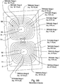
FIG. 5A through FIG. 5C , inclusive, illustrate examples of deformation patterns of the cover or housing member in three different vibrational modes. - In accordance with one embodiment, in
FIG. 1 acover 10 or housing member for anelectronic device 12 comprises acentral region 14 and aperimeter region 26 surrounding thecentral region 14. Thecentral region 14 comprises anelevated pattern 16 ofradial ribs 18 andelliptical elevations 20 elevated above a generally planarlower surface 22. As used herein, a generally planar surface shall include any of the following: a perfectly flat or planar surface, a virtually flat or planar surface, a substantially flat or planar surface, a surface that has immaterial changes in elevation between two reference points on or associated with the surface such that the two reference points do not truly lie in the exact same geometric plane as the surface, or a surface that has an immaterial slope (e.g., less than 1 millimeter in maximum elevation change per centimeter in radial displacement) between a reference point and any radially spaced point on a generally planar surface. - The
elevated pattern 16 is arranged such that thecover 10 has multiple vibrational modes of natural resonance (e.g., at corresponding natural resonant frequencies) in which a maximum deflection or maximum elastic deformation of thecover 10 occurs in each vibrational mode (e.g., first mode at a central point 24) of thecover 10. Thecover 10 or housing member is configured with the elevatedpattern 16 to dampen vibration encountered by the electronic device in on-road ground vehicle applications, off-road ground vehicle applications, or otherwise. Further, thecover 20 may have vibrational modes that are tuned, via the arrangement of the elevatedpattern 16, to dissipate vibrational energy and to increase the natural frequency of resonance over that of a cover or housing member having a generally planar surface. Each mode of vibration for thecover 10 may be associated with a different natural frequency of vibration or a range of different natural frequencies of vibration. - In one embodiment, the
perimeter region 26 has astep 34 and amating flange 36 for mating with theelectronic device 12. As illustrated inFIG. 1 , the edge of theperimeter region 26 terminates in alip 38 extending in an opposite direction (e.g., downward inFIG. 1 ) from theelevated pattern 16. In one configuration, thecentral region 14 is generally rectangular, although thecentral region 14 may be shaped with other geometric shapes, such as substantially polygonal, circular, elliptical, or otherwise. - The
radial ribs 18 andelliptical elevations 20 of the elevatedpattern 16 are spaced apart from each other (or arranged with a target density) to achieve the desired maximum deflection or other vibrational characteristics of thecover 10. The deformation or deflection of thecover 10 is generally elastic and does not result in permanent deformation of thecover 10. As illustrated inFIG. 4A , the desired maximum deflection or elastic deformation may depend upon or comply with aclearance distance 46 between acircuit board 44 or closest component mounted on thecircuit board 44 and theinterior side 23 of thecover 10. Theexterior side 25 of thecover 10 is opposite theinterior side 23. The vibrational characteristics are defined by one or more of the following, among other possible factors: (a) the maximum deflection or elastic deformation of thecover 10 mounted on anelectronic device 12 at or near theperimeter region 26, (b) natural frequency or frequencies of vibration of thecover 10 in a vibrational mode associated with vibrational excitation typical of off-road vehicles, on-road vehicles, or both, (c) increasing the natural frequency of vibration of thecover 10 in one or more vibrational modes by adding structural rigidity to thecover 10 associated with the elevation pattern (e.g., 16), and (d) the dominant vibrational modes of thecover 10 and the corresponding maximum deflection or maximum elastic deformation associated with each dominant vibrational mode in response to vibrational excitation in a frequency range (e.g., approximately zero to two thousand Hertz) and of an amplitude level associated with off-road vehicles. - As shown in
FIG. 1 , theradial ribs 18 are positioned approximately twenty two and one-half degrees apart from each other, although other spacing may provide desired structural rigidity of thecover 10 and vibrational characteristics. Although sixteenradial ribs 18 are illustrated inFIG. 1 , any other number ofradial ribs 18 may be used that provides the desired structural rigidity and vibrational characteristics. - Although there are two
elliptical elevations 20 that are generally concentric about acenter point 24 inFIG. 1 , any other number ofelliptical elevations 20 may be used to achieve the desired vibrational characteristics in conjunction with theradial ribs 18. Because of the generally rectangular shape of thecover 10, the outermostelliptical elevations 20 nearcorners 15 are shaped like arcs or are partially elliptical. The inner-mostelliptical elevations 20 surround thecentral portion 52. - As illustrated in
FIG. 1 , thecenter point 24 lies within thecentral portion 52. Thecentral portion 52 is generally rectangular and has a depressed region 54 that has two generally lineardepressed sections 56 that cross each other. - In one embodiment, the
elevated pattern 16 is formed by stamping a generally planar sheet metal or alloy with or against a die. In one embodiment, the planar sheet metal may comprise steel, a stainless steel alloy or another metal or alloy. In an alternative embodiment, the cover may be formed of another material, such as a polymer, a polymer composite, a plastic, a polymer matrix with a filler (e.g., carbon fiber), or otherwise. In one configuration, theradial ribs 18 andelliptical elevations 20 are within a range of approximately 1 millimeter to approximately 3 millimeters above the generally planarlower surface 22. - The first vibrational mode is illustrated by the double-
headed arrow 31 inFIG. 1 at thecentral point 24. The first mode of vibration of thecover 10 may be excited by any excitation frequency or excitation frequency range (e.g., within a range between zero and two thousand Hertz), although the first mode may be more readily or efficiently excited with an excitation frequency or excitation frequency range that is a positive integer multiple of a natural frequency of resonance or vibration of the first mode, which is elevated above the frequency of natural resonance of a generally planar cover. The double-headedarrow 31 indicates that thecentral point 24 of thecover 10 can move or be deflected up or down by the maximum deflection (e.g., absolute maximum deflection or maximum elastic deformation) or maximum first mode deflection that is specific to the first mode. In the first mode, thecover 10 may oscillate with a first mode frequency (e.g., maximum first mode frequency), which is generally higher than that of a generally planar or reference flat cover, in response to excitation by ground induced vibrations of an off-road or on-road vehicle.FIG. 5A shows the first mode in greater detail thanFIG. 1 and will be described later in this document. - The lower the frequency of natural resonance of the
cover 10 or housing member, the higher the energy in that resonance. Therefore, theelevated pattern 16 is configured to shift the natural resonance of thecover 10 higher in the frequency range for one or more of the vibrational modes. Even a small increase in the first mode frequency, the second mode frequency or the third mode frequency of vibration (e.g., where the mode frequency comprises the frequency of natural resonance) from the design of theelevated pattern 16 may reduce the maximum deflection (e.g., of thecover 10 toward the circuit board 44) and the vibrational energy that theelectronic device 12 or thecircuit board 44 are exposed to. -
FIG. 2 is similar toFIG. 1 , except the double-headedarrows 33 show the illustrative natural vibration in the second mode, as opposed to the first mode ofFIG. 1 . Like reference numbers inFIG. 1 andFIG. 2 indicate like elements. The second mode of vibration of thecover 10 may be excited by any excitation frequency or excitation frequency range (e.g., within a range between zero and two thousand Hertz), although the second mode may be more readily or efficiently excited with an excitation frequency or excitation frequency range that is a positive integer multiple of a natural frequency of resonance or vibration of the second mode, which is elevated above the frequency of natural resonance of a generally planar cover. The double-headedarrows 33 are arranged about thelongitudinal axis 30 which extends longitudinally parallel to the longer side of the generallyrectangular cover 10. The double headedarrows 33 indicate the region of maximum deflection or maximum elastic deformation of the natural resonance or vibration in the second mode. The double-headedarrows 33 indicate the region or point of maximum displacement (e.g., vertical displacement) of thecover 10 with respect to thecircuit board 44 in the second mode. The doubled-headed arrows intercept thelongitudinal axis 30 and two second mode deflection points 28. -
FIG. 3 is similar toFIG. 1 andFIG. 2 , except the double-headedarrows 35 show the illustrative natural vibration in the third mode, as opposed to the first mode ofFIG. 1 or the second mode ofFIG. 2 . Like reference numbers inFIG. 1 ,FIG. 2 , andFIG. 3 indicate like elements. The third mode of vibration of thecover 10 may be excited by any excitation frequency or excitation frequency range (e.g., within a range between zero and two thousand Hertz), although the third mode may be more readily or efficiently excited with an excitation frequency or excitation frequency range that is a positive integer multiple of the natural frequency of resonance or vibration of the third mode, which is elevated above the frequency of natural resonance of a generally planar cover. The double-headedarrows 35 are arranged about thetransverse axis 32 that is perpendicular to thelongitudinal axis 30. As described above, thelongitudinal axis 30 extends longitudinally parallel to the longer side of the generallyrectangular cover 10. The double headedarrows 35 indicate the region of maximum deflection or elastic deformation of the natural resonance or vibration in the third mode. The double-headedarrows 35 indicate the region or point of maximum displacement of thecover 10 with respect to thecircuit board 44 in the third mode. The doubled-headedarrows 35 intercept thetransverse axis 32 and two third mode deflection points 29. -
FIG. 4A is a perspective view of a cross section of the electronics device that is cut-away alongreference line 4A-4A ofFIG. 1 . Like reference numbers inFIG. 1 andFIG. 4A indicate like elements. - As illustrated in
FIG. 4A andFIG. 4B , anelectronic device 12 comprises ahousing 42 having at least oneopen side 40. Acircuit board 44 is secured to or within thehousing 42. For example, thecircuit board 44 may be mounted to thehousing 42 via fasteners (e.g., screws) or via fasteners and stand-offs. As illustrated inFIG. 4A , thecircuit board 44 is attached to thehousing 42 via a centrally mountedscrew 49, although numerous other mounting techniques are possible including, but not limited to, fasteners, clips, adhesives, retainers, card-edge retainers, or snap-fit connections. - The
cover 10 or housing member is arranged for mating with theopen side 40 of thehousing 42. When mounted on thehousing 42, thecover 10 or housing member is spaced apart from thecircuit board 44 or the closest portion (e.g., highest elevation) of the components mounted thereon by aclearance distance 46. Thecover 10 comprises acentral region 14 and aperimeter region 26. Thecentral region 14 comprises anelevated pattern 16 ofradial ribs 18 andelliptical elevations 20 elevated above a generally planarlower surface 22. Theelevated pattern 16 is arranged such that thecover 10 has multiple vibrational modes of natural resonance, including a first vibrational mode, a second vibrational mode, and a third vibrational mode, for example. - In a first mode (e.g., at a first mode vibrational frequency or frequency range of natural resonance for a given excitation energy), a maximum deflection of the
cover 10 occurs at acentral point 24 of thecover 10, where the maximum deflection is less than theclearance distance 46 between theinterior side 23 of thecover 10 and thecircuit board 44 orcomponents 76 mounted thereon. Theclearance distance 46 of the first mode may be aligned with or coincident with the double-headedarrow 31 and thecentral point 24 ofFIG. 1 . - The clearance distance or distances 48 of the second mode (e.g., at a second mode vibrational frequency or frequency range of natural resonance for a given excitation energy) may be aligned with or coincident with the double-headed
arrow 33 of the second mode and the deflection points 28 ofFIG. 2 . Eachclearance distance 48 is between theinterior side 23 of thecover 10 and thecircuit board 44 orcomponents 76 mounted thereon The clearance distance (not shown) of the third mode may be aligned with or coincident with the double-headedarrow 35 of the third mode and deflection points 29 ofFIG. 3 . The clearance distance of the third mode (e.g., at a third mode vibrational frequency or frequency range of natural resonance for a given excitation energy) is between theinterior side 23 of thecover 10 and thecircuit board 44 orcomponents 76 mounted thereon - Movement (e.g., vertical movement) of the
cover 10 interior toward thecircuit board 44 even as small as two millimeters to three millimeters can cause thecircuit board 44 to resonate, which in turn can cause fragile components, like ceramic capacitors to crack or facture. Under one possible failure mode or reliability-reducing mode of thecircuit board 44 that might occur in the absence ofimproved cover 10 set forth herein, thecircuit board 44 might be moved by the rapid movement of air between the alternate cover (e.g., an alternate cover that is a substantially flat or planar cover) thecircuit board 44 as the alternate cover vibrates. Theelectronic device 12 may have theinterior side 23 of thecover 10 as close as possible to thecircuit board 44 with a clearance distance that is greater than or equal to the maximum deflection of thecover 10. The close spacing of thecover 10 to thecircuit board 44 allows theelectronic device 12 to have a compact height or low profile that is useful for mounting theelectronic device 12 in cramped vehicle compartments or in other parts of the vehicle (e.g., such as in the headliner in the vehicle cab). -
FIG. 4B is a perspective exploded view of theelectronics device 12 with thecover 10 or housing member removed to reveal anopen side 40 of thehousing 42 and thecircuit board 44 mounted or secured within thehousing 42. Aseal 50 may intervene between ahousing mating surface 51 and themating surface 53 of thecover 10 or lid. Theseal 50 may comprise a gasket, sealant, an adhesive, or another material for preventing the ingress of moisture, salt, fog, rain, precipitation, dirt, debris, dust or other contaminants from the external environment into thehousing 42 or thecircuit board 44 therein. -
FIG. 4B illustratescomponents 76, such as electronic components, electrical components (e.g., capacitors), semiconductors (e.g., integrated circuits), or other devices mounted on thecircuit board 44.Electrical connectors 78 on the sides of thehousing 42 support one or more electrical connections to thecircuit board 44, conductive traces thereon, orcomponents 76 thereon. - Although the measurement units for the elastic deformation patterns in
FIG. 5A through FIG. 5C , inclusive, are set forth in micrometers (i.e., µm) for illustrative purposes, it should be understood that the units are somewhat arbitrary and will change with the magnitude or amplitude of the excitation energy (e.g., at one or more excitation frequencies) that vibrates thecover 10 or theelectronic device 12. To some extent, the greater the amplitude of the excitation vibrational energy applied to thecover 10 orelectronic device 12, the greater the magnitude of the elastic deformation of thecover 10 tends to be, at least to a limit. As illustrated,FIG. 5A through FIG. 5C , inclusive, use a common amplitude or common reference excitation energy at different excitation frequencies for the sake of ready comparison. - In various embodiments of cover or electronic device, the measurement units or illustrative deformations in
FIG. 5A through FIG. 5C , inclusive, may vary with one or more of the following: the magnitude, frequency or frequencies, waveform (e.g., sinusoidal excitation) and other parameters of the input vibrational energy applied to thecover 10; the thickness of the sheet metal, alloy, polymer, polymer composite or other material used to construct thecover 10; the elasticity or other material properties of the sheet metal, alloy, polymer, polymer composite or other material for thecover 10; the points of attachment (e.g., peripheral attachment or peripheral and central attachment) of the cover to thehousing 42 of the electronic device; the height of the elliptical elevations and radial ribs on thecover 10; and the number or density of elliptical elevations or radial ribs on thecover 10, among other possible factors that fall within the scope of the claims. - In
FIG. 5A , thecover 10 has a first mode of vibration and natural resonance in which the maximum deflection or maximum elastic deformation occurs at acentral point 24 of thecover 10. In one embodiment, the first mode has a lower frequency of natural resonance (of vibration) than the second mode and the third mode, in response to application of excitation energy within a range of approximately zero to approximately two thousand Hertz. The deformation or deflection of thecover 10 is generally elastic and does not result in permanent deformation of thecover 10. Throughout this document and the drawings, references to "deformation" shall mean generally elastic deformation. The greatest elastic deformation of the first mode occurs in an inner-mostelliptical region 500 about thecentral point 24 of thecover 10. The lower elastic deformation of the first mode occurs in a peripheral or outer-most elliptical region 512 about thecentral point 24 of thecover 10. Here, the greatest elastic deformation of the first mode is approximately 158 micrometers, plus or minus ten percent, and the lower elastic deformation is approximately 16 micrometers, plus or minus ten percent, where the excitation frequency (e.g., peak excitation frequency) of vibration (e.g., from the ground of ground engaging vehicle) is around 170 Hertz, plus or minus ten percent, for example. The intermediateelliptical regions 504 have elastic deformations intermediate between the greatest elastic deformation of the first mode and the lesser elastic deformation of the first mode. It should be noted that thecover 10 also can vibrate with lesser deformations (not shown) than the lower elastic deformation between the outer-most elliptical region 512 and theperimeter region 26, but the magnitude of the vibration or deformation is not generally material to dampening of the vibration of theelectronic device 12. - Each elliptical region is associated with a corresponding elastic deformation range in
FIG. 5A . The elastic deformation range of the inner-mostelliptical region 500 is labeled as Deformation Range A (e.g., 140-158 micrometers(µm)) inFIG. 5A . As illustrated, Deformation Range B, C, D, E, F, G and H are progressively lower deformation ranges than Deformation Range A. - In
FIG. 5B , thecover 10 has a second mode of vibration and natural resonance in which the maximum elastic deflection occurs at twodeflection points 28 along alongitudinal axis 30 and spaced approximately equidistant from thecentral point 24 of thecover 10. In one embodiment, the second mode has a higher frequency of natural resonance (of vibration) than the first mode and a lower frequency of natural resonance than the third mode, in response to application of excitation energy within a range of approximately zero to approximately two thousand Hertz. - The greatest or greater elastic deformation of the second mode occurs in dual inner-most
elliptical regions 502 about deflection points 28 of thecover 10. The lesser elastic deformations of the second mode occur in the peripheral or outer-mostelliptical regions 514 about the deflection points 28 of thecover 10. Here, the greater elastic deformation of the second mode is approximately 151 micrometers, plus or minus ten percent, and the lesser elastic deformation is approximately 17 micrometers, plus or minus ten percent, where the excitation frequency (e.g., peak excitation frequency) of vibration (e.g., from the ground of ground engaging vehicle) is around 240 Hertz, plus or minus ten percent, for example. The intermediateelliptical regions 506 have deformations intermediate between the greater elastic deformation of the second mode and the lesser elastic deformation of the second mode. - Each elliptical region is associated with a corresponding deformation range in
FIG. 5B . The elastic deformation range of the inner-mostelliptical region 502 is labeled as Deformation Range A (e.g., 134-151 micrometers(µm)) inFIG. 5B . As illustrated, Deformation Range B, C, D, E, F, G and H are progressively lesser deformation ranges than Deformation Range A. - It should be noted that the
cover 10 also can vibrate with lower deformations (not shown) than the lower elastic deformation between the outer-most elliptical region 512 and theperimeter region 26, but the magnitude of the vibration and associated deformation is not generally material to dampening of the vibration of theelectronic device 12. - In
FIG. 5C , thecover 10 has a third mode of vibration and natural resonance in which the maximum deflection occurs at twodeflection points 29 along atransverse axis 32 and spaced approximately equidistant from thecentral point 24 of thecover 10. In one embodiment, the third mode has a higher frequency of natural resonance (of vibration) than the first mode and a higher frequency of natural resonance than the second mode, in response to application of excitation energy within a range of approximately zero to approximately two thousand Hertz. - The greater maximum elastic deformation of the third mode occurs in the dual inner-most
elliptical regions 600 about the deflection points 29 of thecover 10. The lesser elastic deformation of the third mode occurs in a peripheral or outer-mostelliptical region 612 about the deflection points 29 of thecover 10. Here, the greater elastic deformation of the third mode is approximately 147 micrometers, plus or minus ten percent, and the lesser elastic deformation is approximately 17 micrometers, plus or minus ten percent where the excitation frequency of vibration (e.g., from the ground of ground engaging vehicle) is around 380 Hertz, plus or minus ten percent, for example. The intermediateelliptical regions 604 have deformations intermediate between the greater elastic deformation of the third mode and the lesser elastic deformation of the third mode. - Each elliptical region is associated with a corresponding deformation range in
FIG. 5C . The deformation range of the inner-mostelliptical region 502 is labeled as Deformation Range A (e.g., 130-147 micrometers (µm)) inFIG. 5C . As illustrated, Deformation Range B, C, D, E, F, G and H are progressively lower deformation ranges than Deformation Range A. - It should be noted that the
cover 10 also can vibrate with lesser deformations (not shown) than the lower elastic deformation between the outer-mostelliptical region 612 and theperimeter region 26, but the magnitude of the vibration is not generally material to dampening of the vibration of theelectronic device 12. - The
cover 10 or housing member is configured with theelevated pattern 16 to dampen vibration encountered by the electronic device in on-road ground vehicle applications, off-road ground vehicle applications or otherwise. Theelevated pattern 16 dampens vibrations by reducing the amplitude of elastic deformation of thecover 10, for example. Further, thecover 20 may have vibrational modes that are tuned, via the arrangement of theelevated pattern 16, to dissipate vibrational energy and to increase the natural frequency of resonance over that of a cover or housing member having a generally planar surface. Thecover 10 andelectronic device 12 provides increased resistance to vibrational shock and damage in off-road vehicular environment and the on-road vehicular applications. The natural vibrational frequency in the first mode, the second mode and the third mode is increased over corresponding vibrational modes associated with a generally planar or flat cover to reduce materially the vibrational energy that needs to be dissipated. - In addition, the improved vibrational resistance of the electronic device to external shock and vibration associated with a ground-engaging vehicle, the
cover 10 andelectronic device 12 provide improved thermal dissipation associated with the radial ribs and elliptical elevations of thecover 10. - The reduced vibration and thermal dissipation supports the longevity and reliable operation of the electronic and electrical components (e.g., components 76) and circuitry. Further, the height or profile of the housing (e.g., housing 42) with a
cover 10 mounted on the housing can be minimized by minimizing or reducing the clearance between the circuit board (e.g., circuit board 44) and interior side or interior surface thecover 10 that would otherwise be necessary (e.g., to prevent contact between thecover 10 and thecircuit board 44 or components thereon 78) without the designed maximum deflection and vibrational characteristics of thecover 10 in one or more vibrational modes. - Having described the preferred embodiment, it will become apparent that various modifications can be made without departing from the scope of the invention as defined in the accompanying claims.
Claims (5)
- An electronic device (12) comprising:a housing (42) having at least one open side (40);a circuit board (44) secured within the housing (42);a cover (10) mating with the open side (40) and spaced apart from the circuit board (44) by a clearance distance, the cover (10) comprising a central region (14) comprising a pattern (16) of ribs (18) and a perimeter region (26) surrounding the central region (14), the central region (14) comprising an elevated pattern (16) of radial ribs (18) and elliptical elevations (20) concentric about a center point (24),characterized in that the ribs (18) and elliptical elevations (20) are elevated above a generally planar lower surface (22) facing the housing (42) and formed by stamping a generally planar sheet metal with or against a die and that the interior side of the cover (10) is placed as close as possible to the circuit board (44) with the clearance distance greater than or equal to the maximum deflection of the cover (10).
- The electronic device (12) according to claim 1 wherein the central region (14) is generally rectangular.
- The electronic device (12) according to claim 1 wherein the perimeter region (26) has a step (34) and a mating flange (36) for mating with the housing (42) of the electronic device (12).
- The electronic device (12) according to claim 3 wherein the edge of the perimeter region (26) terminates in a lip (38) extending in an opposite direction from the elevated pattern (16).
- The electronic device (12) according to claim 1 wherein the radial ribs (18) and elliptical elevations (20) are within a range of 1 millimeter to 3 millimeters above the generally planar lower surface.
Applications Claiming Priority (3)
| Application Number | Priority Date | Filing Date | Title |
|---|---|---|---|
| US32000210P | 2010-04-01 | 2010-04-01 | |
| US12/762,514 US8338721B2 (en) | 2010-04-01 | 2010-04-19 | Cover with improved vibrational characteristics for an electronic device |
| PCT/US2011/029696 WO2011123307A1 (en) | 2010-04-01 | 2011-03-24 | Cover with improved vibrational characteristics for an electronic device |
Publications (3)
| Publication Number | Publication Date |
|---|---|
| EP2554029A1 EP2554029A1 (en) | 2013-02-06 |
| EP2554029A4 EP2554029A4 (en) | 2017-06-21 |
| EP2554029B1 true EP2554029B1 (en) | 2019-12-18 |
Family
ID=44708303
Family Applications (1)
| Application Number | Title | Priority Date | Filing Date |
|---|---|---|---|
| EP11763239.8A Active EP2554029B1 (en) | 2010-04-01 | 2011-03-24 | Cover with improved vibrational characteristics for an electronic device |
Country Status (5)
| Country | Link |
|---|---|
| US (1) | US8338721B2 (en) |
| EP (1) | EP2554029B1 (en) |
| CN (1) | CN102972102B (en) |
| BR (1) | BR112012023061B1 (en) |
| WO (1) | WO2011123307A1 (en) |
Families Citing this family (12)
| Publication number | Priority date | Publication date | Assignee | Title |
|---|---|---|---|---|
| DE102008062657A1 (en) * | 2008-12-04 | 2010-06-10 | Stribel Production Gmbh | Energy storage device |
| EP2456040A1 (en) | 2010-11-19 | 2012-05-23 | Flextronic Int.Kft | Circuit for storing electrical energy |
| US9593492B2 (en) * | 2013-09-18 | 2017-03-14 | Senqcia Corporation | Lid member and floor panel using the same |
| US9529389B1 (en) * | 2014-09-25 | 2016-12-27 | Amazon Technologies, Inc. | Variable plated device enclosure |
| US9293870B1 (en) * | 2015-03-10 | 2016-03-22 | Continental Automotive Systems, Inc. | Electronic control module having a cover allowing for inspection of right angle press-fit pins |
| DE102016216177A1 (en) * | 2016-08-29 | 2018-03-01 | Robert Bosch Gmbh | Connector strip for a control unit |
| CN110154716A (en) * | 2018-02-12 | 2019-08-23 | 比亚迪股份有限公司 | Motor controller cover, motor controller and powertrain |
| IT201800007394A1 (en) * | 2018-07-20 | 2020-01-20 | CHARGERS FOR ELECTRIC OR HYBRID VEHICLES | |
| DE102019122812B4 (en) * | 2019-08-26 | 2024-03-14 | Sma Solar Technology Ag | CASE FOR AN ELECTRICAL APPARATUS WITH A COVER AND ELECTRICAL APPARATUS WITH A CASE |
| KR102764498B1 (en) * | 2019-12-12 | 2025-02-10 | 삼성전자주식회사 | Semiconductor module |
| USD944199S1 (en) * | 2020-04-30 | 2022-02-22 | Thermo King Corporation | Low power module for controller of transport climate control system |
| JP2025031129A (en) * | 2023-08-25 | 2025-03-07 | 日立Astemo株式会社 | Electric circuit housing |
Citations (2)
| Publication number | Priority date | Publication date | Assignee | Title |
|---|---|---|---|---|
| US20070008680A1 (en) * | 2005-07-08 | 2007-01-11 | The Agus S | Power converter having housing with improved thermal properties |
| US20090015120A1 (en) * | 2007-07-13 | 2009-01-15 | Tellabs Petaluma, Inc. | Heat dissipation device for electronics cabinet |
Family Cites Families (23)
| Publication number | Priority date | Publication date | Assignee | Title |
|---|---|---|---|---|
| US3346221A (en) * | 1965-02-04 | 1967-10-10 | Sanders Associates Inc | Critically damped vibration system |
| DE3047886A1 (en) | 1979-12-20 | 1981-10-29 | The Fujikura Cable Works, Ltd., Tokyo | METHOD FOR PRODUCING A PUNCHING TOOL AND PUNCHING TOOL PRODUCED BY THIS METHOD |
| DE3409869A1 (en) | 1984-03-17 | 1985-09-19 | Fichtel & Sachs Ag, 8720 Schweinfurt | CLUTCH DISC |
| US4589713A (en) | 1984-04-09 | 1986-05-20 | Raytheon Company | Video display support joint |
| US4635940A (en) | 1985-06-26 | 1987-01-13 | William E. McClure | Dart board assembly for an electronic dart game |
| AT389053B (en) * | 1986-02-17 | 1989-10-10 | Andrae Franz | DEVICE FOR SHIELDING AGAINST AN ELECTROMAGNETIC FIELD |
| JPH03110906A (en) * | 1989-09-26 | 1991-05-10 | Nec Corp | Oscillator |
| US5295029A (en) | 1990-07-31 | 1994-03-15 | Seagate Technology, Inc. | Disk drive including unitary deck for aligning and supporting axially retractable spindle assembly |
| US5212607A (en) | 1990-07-31 | 1993-05-18 | Seagate Technology, Inc. | Disk drive including unitary deck for aligning and supporting axially retractable spindle assembly |
| JP3344925B2 (en) * | 1997-05-26 | 2002-11-18 | 富士通株式会社 | Playback device and storage device |
| JP4121185B2 (en) | 1998-06-12 | 2008-07-23 | 新電元工業株式会社 | Electronic circuit equipment |
| US6188150B1 (en) | 1999-06-16 | 2001-02-13 | Euv, Llc | Light weight high-stiffness stage platen |
| US6407925B1 (en) | 1999-09-17 | 2002-06-18 | Denso Corporation | Casing for electronic control devices |
| JP3648119B2 (en) | 2000-03-01 | 2005-05-18 | 株式会社ケーヒン | Electronic circuit board housing case |
| US6499215B1 (en) * | 2000-06-29 | 2002-12-31 | International Business Machines Corporation | Processing of circuit boards with protective, adhesive-less covers on area array bonding sites |
| US6628523B2 (en) | 2001-02-08 | 2003-09-30 | Denso Corporation | Casing for electronic control unit |
| US6717051B2 (en) | 2001-02-21 | 2004-04-06 | Denso Corporation | Electronic control unit for use in automotive vehicle |
| TWI234765B (en) | 2001-03-29 | 2005-06-21 | Matsushita Electric Industrial Co Ltd | Rotor assembly, information-recording/-reproducing device and method of assembling the rotor assembly |
| JP4136363B2 (en) | 2001-11-29 | 2008-08-20 | キヤノン株式会社 | Positioning apparatus and exposure apparatus using the same |
| JP4211580B2 (en) | 2003-11-18 | 2009-01-21 | 株式会社デンソー | Electronic device housing structure |
| US7476992B2 (en) | 2005-05-17 | 2009-01-13 | Parker-Hannifin Corporation | Air-cooled electric motor |
| DE602007007745D1 (en) | 2007-05-21 | 2010-08-26 | Magneti Marelli Spa | Electronic control unit with a central elastic element |
| US8013258B2 (en) * | 2008-06-11 | 2011-09-06 | Mediatek Inc. | Shielding device |
-
2010
- 2010-04-19 US US12/762,514 patent/US8338721B2/en active Active
-
2011
- 2011-03-24 EP EP11763239.8A patent/EP2554029B1/en active Active
- 2011-03-24 BR BR112012023061A patent/BR112012023061B1/en active IP Right Grant
- 2011-03-24 CN CN201180016994.0A patent/CN102972102B/en active Active
- 2011-03-24 WO PCT/US2011/029696 patent/WO2011123307A1/en not_active Ceased
Patent Citations (2)
| Publication number | Priority date | Publication date | Assignee | Title |
|---|---|---|---|---|
| US20070008680A1 (en) * | 2005-07-08 | 2007-01-11 | The Agus S | Power converter having housing with improved thermal properties |
| US20090015120A1 (en) * | 2007-07-13 | 2009-01-15 | Tellabs Petaluma, Inc. | Heat dissipation device for electronics cabinet |
Also Published As
| Publication number | Publication date |
|---|---|
| EP2554029A1 (en) | 2013-02-06 |
| BR112012023061B1 (en) | 2020-01-28 |
| US20110240361A1 (en) | 2011-10-06 |
| US8338721B2 (en) | 2012-12-25 |
| WO2011123307A1 (en) | 2011-10-06 |
| BR112012023061A8 (en) | 2018-01-02 |
| CN102972102A (en) | 2013-03-13 |
| BR112012023061A2 (en) | 2016-05-17 |
| CN102972102B (en) | 2016-03-30 |
| EP2554029A4 (en) | 2017-06-21 |
Similar Documents
| Publication | Publication Date | Title |
|---|---|---|
| US8338721B2 (en) | Cover with improved vibrational characteristics for an electronic device | |
| US10244645B2 (en) | Electronic control unit with a housing stabilizing element and housing for electronic control unit | |
| CN103890414A (en) | Guarding device with a guarding element and at least one thermally and oscillatingly decoupling fastening device | |
| JP5804252B2 (en) | Grommet | |
| CN1422511A (en) | Fixing plate, fixing arrangement comprising the fixing plate and the use of said fixing plate | |
| US9193052B2 (en) | Mounting system for a gas gun | |
| US10524374B2 (en) | Electric device | |
| JP7148274B2 (en) | electrical equipment | |
| EP2745535B1 (en) | Apparatus comprising an acoustic radiator and a band seal, and method for coupling a passive radiator to an acoustic enclosure. | |
| CN102712309B (en) | System components for automobiles | |
| US7618012B2 (en) | Bracket fixing structure | |
| RU2338344C1 (en) | Protective jacket for radio-electronic devices | |
| JP2020190464A (en) | Acceleration sensor core unit, method for preventing deflection of substrate with acceleration sensor mounted thereon | |
| JP2012026532A (en) | Elastic support tool | |
| JP4606300B2 (en) | Vibration isolator | |
| JP3978586B2 (en) | Anti-vibration support device | |
| WO2012091734A1 (en) | Rugged solid state hard drive with silicone gel damping | |
| JP2006183693A (en) | Vibration insulation system and engine suspension method | |
| JP2018162845A (en) | Mount rubber | |
| JP4930944B2 (en) | Hysteretic damper mounting structure | |
| KR20260045220A (en) | Inverter Assembly | |
| WO1998048197A2 (en) | Vibration control system, especially for circuit boards | |
| CN117246295A (en) | Vacuum pump's installation component and vehicle | |
| JP2025025184A (en) | Lighting fixtures | |
| JP2017092231A (en) | Mounting structure of electronic component |
Legal Events
| Date | Code | Title | Description |
|---|---|---|---|
| PUAI | Public reference made under article 153(3) epc to a published international application that has entered the european phase |
Free format text: ORIGINAL CODE: 0009012 |
|
| 17P | Request for examination filed |
Effective date: 20121102 |
|
| AK | Designated contracting states |
Kind code of ref document: A1 Designated state(s): AL AT BE BG CH CY CZ DE DK EE ES FI FR GB GR HR HU IE IS IT LI LT LU LV MC MK MT NL NO PL PT RO RS SE SI SK SM TR |
|
| DAX | Request for extension of the european patent (deleted) | ||
| RAP1 | Party data changed (applicant data changed or rights of an application transferred) |
Owner name: DEERE & COMPANY |
|
| RA4 | Supplementary search report drawn up and despatched (corrected) |
Effective date: 20170524 |
|
| RIC1 | Information provided on ipc code assigned before grant |
Ipc: H05K 5/00 20060101AFI20170518BHEP |
|
| STAA | Information on the status of an ep patent application or granted ep patent |
Free format text: STATUS: EXAMINATION IS IN PROGRESS |
|
| 17Q | First examination report despatched |
Effective date: 20190329 |
|
| GRAP | Despatch of communication of intention to grant a patent |
Free format text: ORIGINAL CODE: EPIDOSNIGR1 |
|
| STAA | Information on the status of an ep patent application or granted ep patent |
Free format text: STATUS: GRANT OF PATENT IS INTENDED |
|
| INTG | Intention to grant announced |
Effective date: 20190705 |
|
| GRAS | Grant fee paid |
Free format text: ORIGINAL CODE: EPIDOSNIGR3 |
|
| GRAA | (expected) grant |
Free format text: ORIGINAL CODE: 0009210 |
|
| STAA | Information on the status of an ep patent application or granted ep patent |
Free format text: STATUS: THE PATENT HAS BEEN GRANTED |
|
| AK | Designated contracting states |
Kind code of ref document: B1 Designated state(s): AL AT BE BG CH CY CZ DE DK EE ES FI FR GB GR HR HU IE IS IT LI LT LU LV MC MK MT NL NO PL PT RO RS SE SI SK SM TR |
|
| REG | Reference to a national code |
Ref country code: GB Ref legal event code: FG4D |
|
| REG | Reference to a national code |
Ref country code: CH Ref legal event code: EP |
|
| REG | Reference to a national code |
Ref country code: DE Ref legal event code: R096 Ref document number: 602011064098 Country of ref document: DE |
|
| REG | Reference to a national code |
Ref country code: IE Ref legal event code: FG4D |
|
| REG | Reference to a national code |
Ref country code: AT Ref legal event code: REF Ref document number: 1216061 Country of ref document: AT Kind code of ref document: T Effective date: 20200115 |
|
| REG | Reference to a national code |
Ref country code: NL Ref legal event code: MP Effective date: 20191218 |
|
| PG25 | Lapsed in a contracting state [announced via postgrant information from national office to epo] |
Ref country code: LV Free format text: LAPSE BECAUSE OF FAILURE TO SUBMIT A TRANSLATION OF THE DESCRIPTION OR TO PAY THE FEE WITHIN THE PRESCRIBED TIME-LIMIT Effective date: 20191218 Ref country code: SE Free format text: LAPSE BECAUSE OF FAILURE TO SUBMIT A TRANSLATION OF THE DESCRIPTION OR TO PAY THE FEE WITHIN THE PRESCRIBED TIME-LIMIT Effective date: 20191218 Ref country code: LT Free format text: LAPSE BECAUSE OF FAILURE TO SUBMIT A TRANSLATION OF THE DESCRIPTION OR TO PAY THE FEE WITHIN THE PRESCRIBED TIME-LIMIT Effective date: 20191218 Ref country code: FI Free format text: LAPSE BECAUSE OF FAILURE TO SUBMIT A TRANSLATION OF THE DESCRIPTION OR TO PAY THE FEE WITHIN THE PRESCRIBED TIME-LIMIT Effective date: 20191218 Ref country code: BG Free format text: LAPSE BECAUSE OF FAILURE TO SUBMIT A TRANSLATION OF THE DESCRIPTION OR TO PAY THE FEE WITHIN THE PRESCRIBED TIME-LIMIT Effective date: 20200318 Ref country code: NO Free format text: LAPSE BECAUSE OF FAILURE TO SUBMIT A TRANSLATION OF THE DESCRIPTION OR TO PAY THE FEE WITHIN THE PRESCRIBED TIME-LIMIT Effective date: 20200318 Ref country code: GR Free format text: LAPSE BECAUSE OF FAILURE TO SUBMIT A TRANSLATION OF THE DESCRIPTION OR TO PAY THE FEE WITHIN THE PRESCRIBED TIME-LIMIT Effective date: 20200319 |
|
| REG | Reference to a national code |
Ref country code: LT Ref legal event code: MG4D |
|
| PG25 | Lapsed in a contracting state [announced via postgrant information from national office to epo] |
Ref country code: HR Free format text: LAPSE BECAUSE OF FAILURE TO SUBMIT A TRANSLATION OF THE DESCRIPTION OR TO PAY THE FEE WITHIN THE PRESCRIBED TIME-LIMIT Effective date: 20191218 Ref country code: RS Free format text: LAPSE BECAUSE OF FAILURE TO SUBMIT A TRANSLATION OF THE DESCRIPTION OR TO PAY THE FEE WITHIN THE PRESCRIBED TIME-LIMIT Effective date: 20191218 |
|
| PG25 | Lapsed in a contracting state [announced via postgrant information from national office to epo] |
Ref country code: AL Free format text: LAPSE BECAUSE OF FAILURE TO SUBMIT A TRANSLATION OF THE DESCRIPTION OR TO PAY THE FEE WITHIN THE PRESCRIBED TIME-LIMIT Effective date: 20191218 |
|
| PG25 | Lapsed in a contracting state [announced via postgrant information from national office to epo] |
Ref country code: CZ Free format text: LAPSE BECAUSE OF FAILURE TO SUBMIT A TRANSLATION OF THE DESCRIPTION OR TO PAY THE FEE WITHIN THE PRESCRIBED TIME-LIMIT Effective date: 20191218 Ref country code: PT Free format text: LAPSE BECAUSE OF FAILURE TO SUBMIT A TRANSLATION OF THE DESCRIPTION OR TO PAY THE FEE WITHIN THE PRESCRIBED TIME-LIMIT Effective date: 20200513 Ref country code: RO Free format text: LAPSE BECAUSE OF FAILURE TO SUBMIT A TRANSLATION OF THE DESCRIPTION OR TO PAY THE FEE WITHIN THE PRESCRIBED TIME-LIMIT Effective date: 20191218 Ref country code: NL Free format text: LAPSE BECAUSE OF FAILURE TO SUBMIT A TRANSLATION OF THE DESCRIPTION OR TO PAY THE FEE WITHIN THE PRESCRIBED TIME-LIMIT Effective date: 20191218 Ref country code: EE Free format text: LAPSE BECAUSE OF FAILURE TO SUBMIT A TRANSLATION OF THE DESCRIPTION OR TO PAY THE FEE WITHIN THE PRESCRIBED TIME-LIMIT Effective date: 20191218 |
|
| PG25 | Lapsed in a contracting state [announced via postgrant information from national office to epo] |
Ref country code: IS Free format text: LAPSE BECAUSE OF FAILURE TO SUBMIT A TRANSLATION OF THE DESCRIPTION OR TO PAY THE FEE WITHIN THE PRESCRIBED TIME-LIMIT Effective date: 20200418 Ref country code: SK Free format text: LAPSE BECAUSE OF FAILURE TO SUBMIT A TRANSLATION OF THE DESCRIPTION OR TO PAY THE FEE WITHIN THE PRESCRIBED TIME-LIMIT Effective date: 20191218 Ref country code: SM Free format text: LAPSE BECAUSE OF FAILURE TO SUBMIT A TRANSLATION OF THE DESCRIPTION OR TO PAY THE FEE WITHIN THE PRESCRIBED TIME-LIMIT Effective date: 20191218 |
|
| REG | Reference to a national code |
Ref country code: DE Ref legal event code: R097 Ref document number: 602011064098 Country of ref document: DE |
|
| REG | Reference to a national code |
Ref country code: AT Ref legal event code: MK05 Ref document number: 1216061 Country of ref document: AT Kind code of ref document: T Effective date: 20191218 |
|
| PLBE | No opposition filed within time limit |
Free format text: ORIGINAL CODE: 0009261 |
|
| STAA | Information on the status of an ep patent application or granted ep patent |
Free format text: STATUS: NO OPPOSITION FILED WITHIN TIME LIMIT |
|
| PG25 | Lapsed in a contracting state [announced via postgrant information from national office to epo] |
Ref country code: ES Free format text: LAPSE BECAUSE OF FAILURE TO SUBMIT A TRANSLATION OF THE DESCRIPTION OR TO PAY THE FEE WITHIN THE PRESCRIBED TIME-LIMIT Effective date: 20191218 Ref country code: MC Free format text: LAPSE BECAUSE OF FAILURE TO SUBMIT A TRANSLATION OF THE DESCRIPTION OR TO PAY THE FEE WITHIN THE PRESCRIBED TIME-LIMIT Effective date: 20191218 Ref country code: DK Free format text: LAPSE BECAUSE OF FAILURE TO SUBMIT A TRANSLATION OF THE DESCRIPTION OR TO PAY THE FEE WITHIN THE PRESCRIBED TIME-LIMIT Effective date: 20191218 |
|
| REG | Reference to a national code |
Ref country code: CH Ref legal event code: PL |
|
| 26N | No opposition filed |
Effective date: 20200921 |
|
| PG25 | Lapsed in a contracting state [announced via postgrant information from national office to epo] |
Ref country code: AT Free format text: LAPSE BECAUSE OF FAILURE TO SUBMIT A TRANSLATION OF THE DESCRIPTION OR TO PAY THE FEE WITHIN THE PRESCRIBED TIME-LIMIT Effective date: 20191218 Ref country code: SI Free format text: LAPSE BECAUSE OF FAILURE TO SUBMIT A TRANSLATION OF THE DESCRIPTION OR TO PAY THE FEE WITHIN THE PRESCRIBED TIME-LIMIT Effective date: 20191218 |
|
| REG | Reference to a national code |
Ref country code: BE Ref legal event code: MM Effective date: 20200331 |
|
| PG25 | Lapsed in a contracting state [announced via postgrant information from national office to epo] |
Ref country code: LU Free format text: LAPSE BECAUSE OF NON-PAYMENT OF DUE FEES Effective date: 20200324 |
|
| PG25 | Lapsed in a contracting state [announced via postgrant information from national office to epo] |
Ref country code: IT Free format text: LAPSE BECAUSE OF FAILURE TO SUBMIT A TRANSLATION OF THE DESCRIPTION OR TO PAY THE FEE WITHIN THE PRESCRIBED TIME-LIMIT Effective date: 20191218 Ref country code: IE Free format text: LAPSE BECAUSE OF NON-PAYMENT OF DUE FEES Effective date: 20200324 Ref country code: LI Free format text: LAPSE BECAUSE OF NON-PAYMENT OF DUE FEES Effective date: 20200331 Ref country code: CH Free format text: LAPSE BECAUSE OF NON-PAYMENT OF DUE FEES Effective date: 20200331 |
|
| PG25 | Lapsed in a contracting state [announced via postgrant information from national office to epo] |
Ref country code: BE Free format text: LAPSE BECAUSE OF NON-PAYMENT OF DUE FEES Effective date: 20200331 Ref country code: PL Free format text: LAPSE BECAUSE OF FAILURE TO SUBMIT A TRANSLATION OF THE DESCRIPTION OR TO PAY THE FEE WITHIN THE PRESCRIBED TIME-LIMIT Effective date: 20191218 |
|
| PG25 | Lapsed in a contracting state [announced via postgrant information from national office to epo] |
Ref country code: TR Free format text: LAPSE BECAUSE OF FAILURE TO SUBMIT A TRANSLATION OF THE DESCRIPTION OR TO PAY THE FEE WITHIN THE PRESCRIBED TIME-LIMIT Effective date: 20191218 Ref country code: MT Free format text: LAPSE BECAUSE OF FAILURE TO SUBMIT A TRANSLATION OF THE DESCRIPTION OR TO PAY THE FEE WITHIN THE PRESCRIBED TIME-LIMIT Effective date: 20191218 Ref country code: CY Free format text: LAPSE BECAUSE OF FAILURE TO SUBMIT A TRANSLATION OF THE DESCRIPTION OR TO PAY THE FEE WITHIN THE PRESCRIBED TIME-LIMIT Effective date: 20191218 |
|
| PG25 | Lapsed in a contracting state [announced via postgrant information from national office to epo] |
Ref country code: MK Free format text: LAPSE BECAUSE OF FAILURE TO SUBMIT A TRANSLATION OF THE DESCRIPTION OR TO PAY THE FEE WITHIN THE PRESCRIBED TIME-LIMIT Effective date: 20191218 |
|
| PGFP | Annual fee paid to national office [announced via postgrant information from national office to epo] |
Ref country code: DE Payment date: 20250219 Year of fee payment: 15 |
|
| PGFP | Annual fee paid to national office [announced via postgrant information from national office to epo] |
Ref country code: FR Payment date: 20250325 Year of fee payment: 15 |
|
| PGFP | Annual fee paid to national office [announced via postgrant information from national office to epo] |
Ref country code: GB Payment date: 20250327 Year of fee payment: 15 |