EP2552037A1 - Synchronisation equipment and associated method - Google Patents
Synchronisation equipment and associated method Download PDFInfo
- Publication number
- EP2552037A1 EP2552037A1 EP11290338A EP11290338A EP2552037A1 EP 2552037 A1 EP2552037 A1 EP 2552037A1 EP 11290338 A EP11290338 A EP 11290338A EP 11290338 A EP11290338 A EP 11290338A EP 2552037 A1 EP2552037 A1 EP 2552037A1
- Authority
- EP
- European Patent Office
- Prior art keywords
- optical signals
- optical
- delay lines
- synchronization
- delay
- Prior art date
- Legal status (The legal status is an assumption and is not a legal conclusion. Google has not performed a legal analysis and makes no representation as to the accuracy of the status listed.)
- Granted
Links
- 238000000034 method Methods 0.000 title claims description 15
- 230000003287 optical effect Effects 0.000 claims abstract description 192
- 230000002123 temporal effect Effects 0.000 claims abstract description 62
- 230000005540 biological transmission Effects 0.000 claims abstract description 21
- 230000001934 delay Effects 0.000 claims abstract description 14
- 230000000737 periodic effect Effects 0.000 claims abstract description 14
- 230000001360 synchronised effect Effects 0.000 claims description 14
- 230000000903 blocking effect Effects 0.000 claims description 5
- 239000006185 dispersion Substances 0.000 description 25
- 239000010410 layer Substances 0.000 description 13
- 238000001514 detection method Methods 0.000 description 10
- 238000010586 diagram Methods 0.000 description 9
- 239000012792 core layer Substances 0.000 description 6
- 238000005516 engineering process Methods 0.000 description 6
- 230000000694 effects Effects 0.000 description 4
- 230000006978 adaptation Effects 0.000 description 3
- 230000001427 coherent effect Effects 0.000 description 2
- 239000000835 fiber Substances 0.000 description 2
- 230000010363 phase shift Effects 0.000 description 2
- 230000003068 static effect Effects 0.000 description 2
- 230000001960 triggered effect Effects 0.000 description 2
- 208000010119 wrinkly skin syndrome Diseases 0.000 description 2
- 230000002776 aggregation Effects 0.000 description 1
- 238000004220 aggregation Methods 0.000 description 1
- 238000001914 filtration Methods 0.000 description 1
- 230000003116 impacting effect Effects 0.000 description 1
- 230000002441 reversible effect Effects 0.000 description 1
- 239000004065 semiconductor Substances 0.000 description 1
Images




Classifications
-
- H—ELECTRICITY
- H04—ELECTRIC COMMUNICATION TECHNIQUE
- H04Q—SELECTING
- H04Q11/00—Selecting arrangements for multiplex systems
- H04Q11/0001—Selecting arrangements for multiplex systems using optical switching
- H04Q11/0003—Details
-
- H—ELECTRICITY
- H04—ELECTRIC COMMUNICATION TECHNIQUE
- H04B—TRANSMISSION
- H04B10/00—Transmission systems employing electromagnetic waves other than radio-waves, e.g. infrared, visible or ultraviolet light, or employing corpuscular radiation, e.g. quantum communication
- H04B10/25—Arrangements specific to fibre transmission
- H04B10/2507—Arrangements specific to fibre transmission for the reduction or elimination of distortion or dispersion
- H04B10/2513—Arrangements specific to fibre transmission for the reduction or elimination of distortion or dispersion due to chromatic dispersion
- H04B10/25133—Arrangements specific to fibre transmission for the reduction or elimination of distortion or dispersion due to chromatic dispersion including a lumped electrical or optical dispersion compensator
-
- H—ELECTRICITY
- H04—ELECTRIC COMMUNICATION TECHNIQUE
- H04B—TRANSMISSION
- H04B2210/00—Indexing scheme relating to optical transmission systems
- H04B2210/25—Distortion or dispersion compensation
- H04B2210/258—Distortion or dispersion compensation treating each wavelength or wavelength band separately
-
- H—ELECTRICITY
- H04—ELECTRIC COMMUNICATION TECHNIQUE
- H04Q—SELECTING
- H04Q11/00—Selecting arrangements for multiplex systems
- H04Q11/0001—Selecting arrangements for multiplex systems using optical switching
- H04Q11/0005—Switch and router aspects
- H04Q2011/0007—Construction
- H04Q2011/002—Construction using optical delay lines or optical buffers or optical recirculation
-
- H—ELECTRICITY
- H04—ELECTRIC COMMUNICATION TECHNIQUE
- H04Q—SELECTING
- H04Q11/00—Selecting arrangements for multiplex systems
- H04Q11/0001—Selecting arrangements for multiplex systems using optical switching
- H04Q11/0005—Switch and router aspects
- H04Q2011/0007—Construction
- H04Q2011/0035—Construction using miscellaneous components, e.g. circulator, polarisation, acousto/thermo optical
-
- H—ELECTRICITY
- H04—ELECTRIC COMMUNICATION TECHNIQUE
- H04Q—SELECTING
- H04Q11/00—Selecting arrangements for multiplex systems
- H04Q11/0001—Selecting arrangements for multiplex systems using optical switching
- H04Q11/0005—Switch and router aspects
- H04Q2011/0037—Operation
- H04Q2011/0045—Synchronisation
Definitions
- the present invention relates to the field of optical transmissions and in particular of the synchronization of optical signals.
- the telecommunication networks of the state of the art are organized in different layers from the access layer to the core layer through the metro or distribution layer.
- the core layer uses circuit transmission technology where resources are reserved almost permanently for a given connection whereas the access layer uses packet switching technologies wherein resources are shared between different connections with a packet granularity.
- a proposed solution of the state of the art is to develop point to multi-point connections in the metro layer which is generally a ring line so that fast switching elements are required only on the reception side of the nodes which provides an improvement of the use of resources while limiting the required investments to modify the existing infrastructures.
- Such absence of synchronization can be due to an absence of synchronization at the emission of the signals but other physical parameters may also introduce a packet temporal shift.
- signals are transmitted through a plurality of multiplexed channels using wavelength division multiplexing technology which means that the different channels are transmitted on different wavelengths and therefore undergone different chromatic dispersion leading to temporal shifts between the packets at the reception node.
- chromatic dispersion compensation methods have been disclosed in the state of the art such as fibers featuring negative chromatic dispersion implemented from node to node.
- PDM-QPSK Polarization-Division Multiplexed-Quadrature Phase Shift Keying
- the present invention refers to a synchronization device for synchronizing a plurality of multiplexed optical signals after transmission through a plurality of wavelength division multiplexing channels along an optical line, the said optical signals comprising data packets aimed at being detected separately and the said synchronization device comprising a wavelength selective switch, a plurality of delay lines having distinct fixed delays, multiplexing means adapted for multiplexing a plurality of demultiplexed optical signals received from the plurality of delay lines, wherein the said wavelength selective switch is configured to:
- the synchronization device comprises control means adapted to:
- the multiplexing means comprise a second wavelength selective switch configured to:
- the multiplexing means comprise a plurality of optical circulators, the number of which corresponds to the number of delay lines, located between the wavelength selective switch and the plurality of delay lines, the said delay lines being looped on the said optical circulators so that the synchronized optical signals at the output of the delay lines are sent back to the wavelength selective switch to be multiplexed.
- the optical signals comprise data packets and inter-packet gaps, the duration of a data packet and an inter-packet gap corresponding to a time slot, the said time slots being of equal duration and wherein the delays of the delay lines correspond to an arithmetic progression with an increment equals to the time slot duration divided by the number of delay lines.
- the required accuracy for the synchronization of the optical signals is related to a desired ratio between the inter-packet gap duration and the time slot duration so that the number of delay lines is determined in function of the said desired ratio, the required number of delay lines being equal to the closest integer being equal or higher than two divided by the said desired ratio.
- the embodiments of the present invention also refer to an optical node located in a point to multi-point optical line transmitting optical signals comprising data packets through wavelength division multiplexing channels, the said optical node comprising:
- the optical node comprises a second synchronization device set in parallel of the first synchronization device and a first and a second fast switching optical gate linked respectively to the first and second synchronization equipment and configured so that the first fast switching optical gate is in a passing mode while the second is in a blocking mode and conversely in order to transmit the optical signals outputted by one of the synchronization device and allow reconfiguration of a synchronization device without loosing data.
- the optical node comprises an optical amplifier in between the at least one synchronization device and the at least one wavelength selector.
- the embodiments of the present invention also refer to a method for synchronizing a plurality of multiplexed optical signals after transmission through a plurality of wavelength division multiplexing channels along an optical line, the said optical signals comprising data packets aimed at being detected separately and the said method comprising the following steps:
- the method is such that:
- the steps of demultiplexing and distributing arc achieved by a wavelength selective switch and in case of a drift of the temporal shift on at least one of the channels larger than a predetermined value, the wavelength selective switch is reconfigured in order to adapt the distribution according to the modified values of undergone temporal shift.
- the predetermined value corresponds to a drift of half the delay increment.
- WDM Wavelength Division Multiplexing
- WSS Wavelength Selective Switch
- decibel unit As used herein, the term “dB" refers to the decibel unit
- the embodiments of the present invention refer to a method for synchronizing optical signals having undergone different temporal shifts due notably to chromatic dispersion during transmission through wavelength division multiplexing channels from a source node to a destination node, the said optical signals comprising optical packets aimed at being detected separately. Indeed, in the case of a point-to-multipoint connection, packets having different destination nodes are transmitted through a common channel so that detection needs to be achieved with a packet granularity.
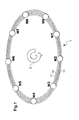
- Fig.1 represents an example of metro layer network in the shape of a WDM ring configured for point-to-multipoint connections wherein, as mentioned above, a packet granularity is required at reception. Nevertheless, it has to be noted that the present invention is not limited to a ring network but can be applied to any point-to-multipoint line configuration.
- the transmission is achieved in only one direction along the ring line, for example the clockwise direction as indicated by the arrow 3.
- Each node Ni has a set of channels reserved for its transmission toward the other nodes Ni so that it can emit signals according to a circuit transmission technology and a unique channel can be used to transmit data packets toward different nodes Ni.
- fast switching elements arc necessary for selecting the wavelength channel comprising the packet needing to be dropped and detesting the said packet among the packets transmitted on the said selected channel.
- the detection refers to a temporal detection as only one packet is transmitted at a time on a given channel.
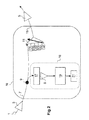
- Figure 2 represents a diagram of an example of an optical node Ni architecture based on an off-line synchronization of the optical signals.
- the optical line 1 is connected to an input 7 of the node Ni.
- An optical amplifier 5 for example an Erbium-Doped Fiber Amplifier (EDFA), is also located on the optical line 1 just before the node Ni to compensate for the power loss undergone during transmission along the optical line 1 and to anticipate a power loss induced in the node Ni.
- EDFA Erbium-Doped Fiber Amplifier
- optical amplifiers 5 represented in Fig.2 and also in the following of the description may be optional if the signal power is high enough to provide the desired signal to noise ratio at destination, that is to say at the burst mode receiver 21 of the destination node.
- the optical line 1 is linked to an optical coupler 9.
- the received optical signals are transmitted toward two different directions:
- the burst mode receiver can detect only one packet at a time, only one channel is transmitted by the wavelength selector 19.
- the wavelength selector 19 achieves the selection of the channel comprising the packet needing to be dropped and the burst mode receiver detects the said packet located on the selected time slot. Besides, it has to be noted that the configuration of the elements of the reception equipment 16 is achieved by the control plane. Thus, for each time slot, the wavelength selector 19 is configured to select the channel comprising the packet that needs to be dropped so that the said packet is received by the burst mode receiver to retrieve the corresponding data.
- Fig.3 represents a diagram of the structure of a first embodiment of the synchronization device 17.
- the multiplexed optical signals received at the input 23 of the synchronization device 17 are sent to the multiplexed port 33 of a first wavelength selective switch (WSS) 25a having a plurality of demultiplexing ports 35 linked to a plurality of delay lines 27.
- the WSS 25a is configured to receive and demultiplex, the optical signals transmitted on the different channels Cj and distribute the said demultiplexed signals toward the delay lines 27 according to their temporal shift with respect to the start of the next period of a periodic temporal reference, a period of the said periodic temporal reference corresponding to a time slot duration.
- Each delay line 27 presents a fixed delay which is distinct or different than the delay presented by the other delay lines 27.
- the delays of the delay lines 27 correspond to the members of an arithmetic progression having a predetermined increment and the value of the said increment, which is linked to the number of delay lines 27, is determined in function of the accuracy required for the synchronization.
- the largest required delay corresponds to the duration of a time slot of the optical signal, the said time slot corresponding to the duration of a packet (header+payload) and an inter-packet gap, said duration being the same for all the packets within the considered network.
- the increment corresponds therefore to a time slot duration divided by the number of delay lines 27.
- the accuracy of the synchronization is also linked to the ratio between the inter-packet gap duration and the time slot duration.
- the more accurate the synchronization the smaller the required ratio between the inter-packet gap duration and the time slot duration.
- clients make requests comprising their desired ratio between the inter-packet gap duration and the time slot duration.
- the required number of delay lines is therefore equal to the closest integer being equal or higher than two divided by the ratio between the inter-packet gap duration and the time slot duration.
- the number of delay lines 27 of the synchronization device is therefore independent of the number of wavelength channels received on its input 23.
- optical signals corresponding to several channels Cj can be sent to a common delay line 27 which is the case when the temporal shift due to chromatic dispersion undergone by said optical signals is approximatively the same, that is to say, when the difference between the said temporal shift, is smaller than half the delay increment.
- the delay lines 27 are also linked on their other side corresponding to the outputs of the said delay lines 27 to a second WSS 25h.
- This second WSS 25b is configured to receive and multiplex the optical signals received from the plurality of delay lines 27 and being synchronized.
- the configuration of the said second WSS 25b is the same as the first WSS 25a but used in the opposite direction to re-multiplexed the plurality of optical signals into one multiplexed signal to be transmitted toward the output 29 of the synchronization device 17.
- Fig.4 represents an example of transmission of different packets in an optical line 1 and the effect of the chromatic dispersion on the optical packets.
- three different channels C1, C2 and C3 are considered.
- the left part of the figure represents the packets during emission at the ingress node also called source node, the x-axis representing the time t. Two packets for each channel are represented.
- packets of the different channels are not synchronized at the emission which is represented by the temporal shift between the packets of the different channels,
- packets P1, P1' and P1" start to be emitted within a time slot ts1 between T0 and T0+Ts, a time slot corresponding to the packet duration tp (comprising the header and the payload) and the inter-packet gap duration tg.
- Packets P2, P2' and P2" start to be emitted in a time slot ts2.
- all the packets, inter-packet gaps and therefore time slots have all the same duration for all the optical signals within the considered network.
- the right part of the figure represents the reception of the packets after transmission through the optical line 1.
- the temporal shift between the packets of the different channel C1, C2, C3 at the reception is not the same as the temporal shift at the emission due to the effects of the chromatic dispersion undergone by the different channels, the said effects being different from one channel to another due to the difference of wavelength between the different channels.
- a temporal shift can be defined between the start of a packet and the start of the next period of the periodic temporal reference.
- the said temporal shifts are represented herein by the references ⁇ , ⁇ ' and ⁇ " respectively for the packet P1 with respect to T2, for the packet P1' with respect to T2 and for the packet P1" with respect to T3.
- the temporal shift undergone through the transmission is such that packet P1" docs not belong to the same time slot as packet P1 and P1' anymore.
- packet P1" is therefore synchronized with the start, of the following period of the periodic reference which corresponds to instant T3 in the present case. Then, the packets are synchronized with the start of the following period of the periodic reference. Indeed, such synchronization allows to use the wavelength selector 19 and the burst mode receiver 21 in combination to retrieve a packet for each time slot.
- packets are directed toward a delay line 27 in function of their temporal shift with respect to the following period of the periodic reference so that the delay is the closest as the the temporal shift.
- packets P1, P1' and P1" are directed toward delay lines 27 having delays as close as possible of respectively ⁇ , ⁇ ' and ⁇ ".
- Fig.5 shows the result of a synchronization using the synchronization device 17 presented in figure 3 .
- the obtained synchronization is not perfect and small time shifts ⁇ 1 and ⁇ 2 may remain between packets P1 and P1' and packets P2 and P1" which are packets of a common time slot.
- this small time shifts ⁇ 1 and ⁇ 2 arc smaller than half of the increment delays and as described previously, this increment is as small as the number of delay lines 27 is large.
- the synchronization level provided by the synchronization device 17 is adjusted (by the number of delay lines 27) to be sufficient to allow the correct processing of the packets by a wavelength selector 19 and a burst mode receiver 21.
- the presence of an inter-packet gap between two consecutive packets allows to the burst mode receiver 21 to retrieve packets being not perfectly synchronized by using a burst duration slightly larger than the packet duration tp.
- the chromatic dispersion is not a fixed parameter and may vary over time, for example due to temperature variations, so that chromatic dispersion compensation needs to be adapted to the said variations in order to avoid a drift of the undergone temporal shift large enough so that the time shift of the corresponding packets would lead to a loss of data at the burst mode receiver 21 level.
- the flexibility of a WSS 25 (reference 25 refers herein to any of the WSS 25a, 25b or 25c) is used to achieve such adaptation of the chromatic dispersion variations.
- a reconfiguration of the WSS 25 allows to transmit the optical signals corresponding to the impacted channels toward delay lines 27 having a delay adapted to the newly undergone chromatic dispersion.
- Such adaptation to variations of the temporal shift requires detection means adapted to detect a chromatic dispersion variation or any variation of the temporal shift with respect to a predetermined value.
- the drift of temporal shift undergone by the packets due to a chromatic dispersion variation is detected at the burst mode receiver 21 level so that the detection means correspond to the at least one burst mode receiver 21.
- the at least one burst mode receiver 21 determines the settings allowing a packet to be centered within a burst slot. Then, during normal mode functioning, the said at least one burst mode receiver 21 is capable of detecting a drift of a packet away from the predetermined value which is the center of the burst slot.
- the optical node Ni comprises control means adapted to receive information from the detection means about the undergone temporal shift variations due to the chromatic dispersion variations and process the said information, for example by comparing the value of the temporal shift with a predetermined value over time, in order to detect a drift of said temporal shift larger that said predetermined value on at least one of the channels Cj and trigger the reconfiguration of the WSS 25 if it is necessary to adapt the distribution of the multiplexed optical signals toward the plurality of delay lines 27 to take into account the drift of temporal shift.
- the reconfiguration of the WSS 25 is triggered if the chromatic dispersion variation or temporal packet drift in our case exceeds a predetermined value on at least one of the channels, for example, an amount or drift corresponding to half of the delay increment between two consecutive delay lines.
- a predetermined value for example, an amount or drift corresponding to half of the delay increment between two consecutive delay lines.
- other conditions can be chosen to trigger the reconfiguration of the WSS 25.
- the reconfiguration of the WSS 25 allows then to transmit the optical signals corresponding to the channels impacted by a chromatic dispersion variation toward a delay line 27 having a delay adapted to their newly undergone chromatic dispersion. It has to be noted that in the structure described in figure 3 , both WSS 25a and 25b have to be reconfigured.
- the time required for the reconfiguration of a WSS 25 is much larger than the order of a packet duration.
- a WSS 25 reconfiguration time is usually larger than 100ms whereas a packet duration is approximately a few micro-seconds. Even if the number of reconfigurations is limited, a few times per day for example, a single reconfiguration would lead to a loss of a large amount of data.
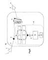
- figure 6 represents a node structure according to an embodiment of the present invention wherein a second synchronization device 17 is set in parallel to the first synchronization device 17.
- the node structure described in figure 6 comprises two synchronization device 17 having their input linked to the optical coupler 9 linked itself to the input 7 of the node Ni, the optical coupler 9 transmitting all the optical signals to both synchronization devices 17.
- the output of each synchronization device 17 is linked to a fast switching optical gate 31.
- the said fast switching optical gates 31 are configured such that the first one is in a passing mode while the other is in a blocking mode and conversely, the passing mode corresponding to a configuration where all the optical signals received on the input are transmitted to the output and the blocking mode corresponding to a configuration where all the optical signals received on the input are blocked.
- the presented structure avoids the amount of data loss if the switching happens when the inter packet gaps go through these gates.
- SOA semiconductor optical amplifier
- a node structure with several wavelength selectors 19 and burst mode receivers 21 working in parallel may also be implemented to allow the detection of several packets at a time as represented in figure 7 in the case of the structure presented in figure 6 with two branches in parallel comprising each a wavelength selector 19 and a burst mode receiver 21.
- redundancy of wavelength selectors 19 and burst mode receivers 21 can be adapted to the structure presented in figure 2 by introducing an optical coupler 9 linked to the output of the optical amplifier 5 linked itself to the output of the Synchronization device 17, the said optical coupler 9 transmitting the optical signals toward the plurality of wavelength selectors 19.
- the optical coupler 9 linked to the output of the fast switching optical gates 31 is used to transmit the signals toward the two branches in parallel, each branch comprising an optical amplifier 5, a wavelength selector 19, and a burst mode receiver 21.
- the distribution between the two burst mode receivers 21 is achieved by the wavelength selectors 19 such that one of the packet needing to be dropped is transmitted to the first burst mode receiver 21 and the second packet needing to be dropped is transmitted to the second burst mode receiver 21, all the other channels being blocked by the wavelength selectors 19.
- the structure of the synchronization device 17 is realized with only one WSS 25e used for both the demultiplexing and the multiplexing.
- a WSS 25 is reversible, which means that it can be used in both directions, and as the configuration of the WSS 25 is the same for the demultiplexing and the multiplexing, a unique WSS 25c can be used for both the demultiplexing and the multiplexing .
- the input 23 of the synchronization device 17 is linked to an optical circulator 34a which transmit the received multiplexed optical signals to the multiplexing ports 33 of the WSS 25c.
- Each demultiplexing port 35 of the WSS 25c is linked to an optical circulator 34 and the delay lines 27 arc looped on the said optical circulators 34 so that the demultiplexed optical signals coming from the demultiplexing ports 35 are transmitted through the optical circulators 34 to the corresponding delay lines 27 and then back to the optical circulators 34 and the demultiplexing ports 35 after transmission through the delay lines 27.
- the synchronized demultiplexed optical signals are then re-multiplexed by the WSS 25c.
- the re-multiplexed optical signals are then transmitted back to the optical circulator 34a linked to the multiplexed port 33 of the WSS 25c and sent to the output 29 of the synchronization device 17.
- Such synchronization device 17 can also be implemented in a node structure as presented in figures 2 , 6 and 7 .
- an example will now be described based on an optical node N3 located on an optical ring line 1 comprising 20 WDM channels C1, C2...C20 among which 3, for example C1, C2 and C3 are reserved for the emission of the optical node N3 and wherein the required synchronization accuracy corresponds to an inter-packet gap being 35% of the time slot duration (in practice, the number of WDM channels and the required synchronization accuracy arc higher).
- the optical node N3 also comprises two branches having each a wavelength selector 19 and a burst mode receiver 21 so that two different packets can be detected at each time slot.
- a 35% ratio of the inter-packet gap to the time slot duration corresponds to a synchronization accuracy of 35/2 ⁇ 17% so that the required number of delay lines is 1/0,17 ⁇ 6.
- the synchronisation devices used in the present example comprise 6 delay lines noted DL1, DL2, DL3, DL4, DL5 and DL6 as represented in figure 9 .
- a synchronization device 17, for example the first one located on the left, is then configured accordingly, which means the gate 31 linked to said first synchronization device 17 is in a passing mode.
- the first wavelength selector 19 is configured to transmit the optical packet of the channel C5 toward the first burst mode receiver 21 and to block the other channels and the second wavelength selector 19 is configured to transmit the optical packet of the channel C16 toward the second burst mode receiver 21 and to block the other channels.
- Besides transmitters 13 are configured to emit optical signals respectively on wavelength corresponding to channel C1, C2 and C3.
- the emitted optical signals may be destined to any other nodes located on the optical ring line 1.
- optical signals comprising data packets can be transmitted between the different nodes.
- a drift of the optical packets is observed at the burst mode receivers 21 level.
- the information of this drift is transmitted from the burst mode receivers to the control means of the synchronization device 17 so that when, for example, this drift reaches a predetermined reconfiguration threshold for channels C15 and C20, a reconfiguration of the WSS 25 is triggered.
- the said reconfiguration comprises the determination of the delay lines 17 toward which the optical signals of the channels C15 and C20 have to be transmitted.
- the new determined configuration is as given below:
- the newly determined configuration is applied on the WSSs 25 of the second synchronization 17 device located on the right and when the reconfiguration of the WSSs 25 of the second synchronization device 17 is over, the gates 31 are switched so that the one linked to the first synchronization device 17 becomes in a blocking mode whereas the one linked to the second synchronization device 17 becomes in a passing mode. If, afterwards, another reconfiguration of the Synchronization device is needed, such reconfiguration will then be achieved on the first synchronization device 17 and so on.
- This reconfiguration also occurs when the wavelength distribution between the different ring nodes is rearranged.
- the structure of the synchronization device 17 and the optical node Ni allows the synchronization of the optical signals without requiring chromatic dispersion compensation equipments, allows to limit the number of required delay line 27 according to the required synchronization accuracy and allows to adapt to the chromatic dispersion variations thanks to the flexibility of the WSS 25.
- the presented structures allow to introduce a point-to-multipoint capability to the metre layer compatible with considered future technologies using advanced modulation formats such as Polarization-Division Multiplexed-Quadrature Phase Shift Keying (PDM-QPSK) with coherent detection.
- PDM-QPSK Polarization-Division Multiplexed-Quadrature Phase Shift Keying
Landscapes
- Engineering & Computer Science (AREA)
- Computer Networks & Wireless Communication (AREA)
- Physics & Mathematics (AREA)
- Electromagnetism (AREA)
- Signal Processing (AREA)
- Optical Communication System (AREA)
Abstract
- a wavelength selective switch (25),
- a plurality of delay lines (27) having distinct fixed delays,
- multiplexing means adapted for multiplexing a plurality of demultiplexed optical signals received from the plurality of delay lines, wherein the said wavelength selective switch (25) is configured to:
- receiver the said plurality of multiplexed optical signals,
- demultiplex the said plurality of received multiplexed optical signals and,
- distribute the demultiplexed optical signals toward the said plurality of delay lines (27) according to a temporal shift of the demultiplexed optical signals with respect to the start of the next period of a periodic temporal reference, a demultiplexed optical signal being transmitted to a delay line (27) having the closest fixed delay with respect to the temporal shift of the said optical demultiplexed optical signal ,
and wherein the number of delay lines (27) is determined according to the required accuracy for the synchronization of the optical signals.
Description
- The present invention relates to the field of optical transmissions and in particular of the synchronization of optical signals.
- The telecommunication networks of the state of the art are organized in different layers from the access layer to the core layer through the metro or distribution layer.
- Needs for the three layers are different as the traffic in the access network is very bursty and therefore requires a relatively small switching granularity, to handle data while maximizing the utilization of the physical resources whereas signals in the core layer correspond to the aggregation of the signals coming from the access layer through the metro layer so that the traffic in the core layer is more stable. Thus, the core layer uses circuit transmission technology where resources are reserved almost permanently for a given connection whereas the access layer uses packet switching technologies wherein resources are shared between different connections with a packet granularity.
- In the case af the metro layer, which is the intermediate layer between the access and the core layer, the trend until now was to use circuit transmission technologies. However, as the traffic is more bursty than in the core layer, some resources arc wasted which becomes a problem as the operators tend to optimize the use of their resources to increase their networks capacities.
- Thus, a proposed solution of the state of the art is to develop point to multi-point connections in the metro layer which is generally a ring line so that fast switching elements are required only on the reception side of the nodes which provides an improvement of the use of resources while limiting the required investments to modify the existing infrastructures.
- However, in order to use fast switching elements and retrieve the transmitted packets, synchronization of the different multiplexed signals received at destination is necessary in order to avoid losses of data.
- Such absence of synchronization can be due to an absence of synchronization at the emission of the signals but other physical parameters may also introduce a packet temporal shift.
- Indeed, signals are transmitted through a plurality of multiplexed channels using wavelength division multiplexing technology which means that the different channels are transmitted on different wavelengths and therefore undergone different chromatic dispersion leading to temporal shifts between the packets at the reception node.
- In order to overcome this problem, chromatic dispersion compensation methods have been disclosed in the state of the art such as fibers featuring negative chromatic dispersion implemented from node to node. However, such solution is not adapted to the future evolution of networks using advanced modulation formats such as Polarization-Division Multiplexed-Quadrature Phase Shift Keying (PDM-QPSK) with coherent detection as such type of detection is more effective without chromatic dispersion compensation.
- Furthermore, the implementation of active elements along the line handling each wavelength separately requires extra filtering stages and introduces additional losses impacting the transmission reach of the optical signals.
- It is therefore an object of the present invention to provide a solution allowing synchronization of the optical signals while overcoming the above-mentioned drawbacks.
- Thus, the present invention refers to a synchronization device for synchronizing a plurality of multiplexed optical signals after transmission through a plurality of wavelength division multiplexing channels along an optical line, the said optical signals comprising data packets aimed at being detected separately and the said synchronization device comprising a wavelength selective switch, a plurality of delay lines having distinct fixed delays, multiplexing means adapted for multiplexing a plurality of demultiplexed optical signals received from the plurality of delay lines, wherein the said wavelength selective switch is configured to:
- receive the said plurality of multiplexed optical signals,
- demultiplex the said plurality of received multiplexed optical signals and,
- distribute the demultiplexed optical signals toward the said plurality of delay lines according to a temporal shift of the demultiplexed optical signals with respect to the start of the next period of a periodic temporal reference, a demultiplexed optical signal being transmitted to a delay line having the closest fixed delay with respect to the temporal shift of the said optical demultiplexed optical signal,
- According to another embodiment of the present invention, the synchronization device comprises control means adapted to:
- receive information about a change in the temporal shift of demultiplexed optical signals with respect to the start of the next period of a periodic temporal reference,
- compare the said temporal shift with a predetermined value over time in order to detect a drift of the said temporal shift,
in case of a drift of the said temporal shift larger than the predetermined value on at least one channel, - trigger a reconfiguration of the wavelength selective switch to adapt the distribution of the demultiplexed optical signals toward the plurality of delay lines to take into account the drift of the said temporal shift.
- According to a further embodiment of the present invention, the multiplexing means comprise a second wavelength selective switch configured to:
- receive the synchronized optical signals at the output of the delay lines and,
- multiplex the said synchronized optical signals.
- According to an additional embodiment of the present invention, the multiplexing means comprise a plurality of optical circulators, the number of which corresponds to the number of delay lines, located between the wavelength selective switch and the plurality of delay lines, the said delay lines being looped on the said optical circulators so that the synchronized optical signals at the output of the delay lines are sent back to the wavelength selective switch to be multiplexed.
- According to another embodiment of the present invention, the optical signals comprise data packets and inter-packet gaps, the duration of a data packet and an inter-packet gap corresponding to a time slot, the said time slots being of equal duration and wherein the delays of the delay lines correspond to an arithmetic progression with an increment equals to the time slot duration divided by the number of delay lines.
- According to a further embodiment of the present invention, the required accuracy for the synchronization of the optical signals is related to a desired ratio between the inter-packet gap duration and the time slot duration so that the number of delay lines is determined in function of the said desired ratio, the required number of delay lines being equal to the closest integer being equal or higher than two divided by the said desired ratio.
- The embodiments of the present invention also refer to an optical node located in a point to multi-point optical line transmitting optical signals comprising data packets through wavelength division multiplexing channels, the said optical node comprising:
- a reception equipment and,
- an optical coupler configured to transmit the optical signals received on the line toward the reception eq uipment,
wherein the reception equipment comprises: - a synchronization device in accordance with one of the previous claims,
- at least one wavelength selector linked to the synchronization equipment configured to select a wavelength channel comprising a data packet needing to be dropped,
- at least one burst mode receiver linked to the at least one wavelength selector configured to retrieve data of the data packets transmitted by the said at least one wavelength selector.
- According to another embodiment of the present invention, the optical node comprises a second synchronization device set in parallel of the first synchronization device and a first and a second fast switching optical gate linked respectively to the first and second synchronization equipment and configured so that the first fast switching optical gate is in a passing mode while the second is in a blocking mode and conversely in order to transmit the optical signals outputted by one of the synchronization device and allow reconfiguration of a synchronization device without loosing data.
- According to a further embodiment of the present invention, the optical node comprises an optical amplifier in between the at least one synchronization device and the at least one wavelength selector.
- The embodiments of the present invention also refer to a method for synchronizing a plurality of multiplexed optical signals after transmission through a plurality of wavelength division multiplexing channels along an optical line, the said optical signals comprising data packets aimed at being detected separately and the said method comprising the following steps:
- demultiplexing the said plurality of received multiplexed optical signals and,
- distributing the demultiplexed optical signals toward a plurality of delay lines having fixed distinct delays according to a temporal shift of the demultiplexed optical signals with respect to the start of the next period of a periodic temporal reference, a demultiplexed optical signal being transmitted to a delay line having the closest fixed delay with respect to the temporal shift of the said demultiplexed optical signal, the number of delay lines being determined according to the required accuracy for the synchronization of the optical signals,
- multiplexing the synchronized optical signals at the outputs of the delay lines.
- According to a further embodiment of the present invention, the method is such that:
- the optical signals comprise data packets and inter-packet gaps, the duration of a data packet and an inter-packet gap corresponding to a time slot, the time slots being of equal duration,
- the delays of the delay lines correspond to an arithmetic progression with an increment corresponding to the time slot duration divided by the number of delay lines,
- the number of delay lines is determined in function of the desired ratio between the inter-packet gap duration and the time slot duration, the required number of delay lines being equal to the closest integer being equal or higher than two divided by the said desired ratio.
- According to an additional embodiment of the present invention, the steps of demultiplexing and distributing arc achieved by a wavelength selective switch and in case of a drift of the temporal shift on at least one of the channels larger than a predetermined value, the wavelength selective switch is reconfigured in order to adapt the distribution according to the modified values of undergone temporal shift.
- According to another embodiment of the present invention, the predetermined value corresponds to a drift of half the delay increment.
-
-
FIG.1 is a diagram of an example embodiment of a metro layer configured as a WDM ring network; -
FIG.2 is a diagram of a first embodiment of the structure of an optical node of the ring network presented inFig.1 . -
FIG.3 is a diagram of a synchronization device according to a first embodiment of the present invention; -
FIG.4 is a representation of the effect of the chromatic dispersion on the synchronization of the packets after transmission along an optical line. -
FIG.5 is a representation of the result of a synchronization process according to the present invention on the received packets represented infig.4 . -
FIG.6 is a diagram of a second embodiment of the structure of an optical node of the ring network presented inFig.1 . -
FIG.7 is a diagram of a third embodiment of the structure of an optical node of the ring network presented inFig.1 . -
FIG.8 is a diagram of a synchronization device according to a second embodiment of the present invention; -
FIG.9 is a diagram of a detailed structure of an optical node according to a given configuration; - As used herein, the term "WDM" refers to the acronym Wavelength Division Multiplexing;
- As used herein, the term "WSS" refers to the acronym Wavelength Selective Switch;
- As used herein, the term "dB" refers to the decibel unit;
- The embodiments of the present invention refer to a method for synchronizing optical signals having undergone different temporal shifts due notably to chromatic dispersion during transmission through wavelength division multiplexing channels from a source node to a destination node, the said optical signals comprising optical packets aimed at being detected separately. Indeed, in the case of a point-to-multipoint connection, packets having different destination nodes are transmitted through a common channel so that detection needs to be achieved with a packet granularity.
-
Fig.1 represents an example of metro layer network in the shape of a WDM ring configured for point-to-multipoint connections wherein, as mentioned above, a packet granularity is required at reception. Nevertheless, it has to be noted that the present invention is not limited to a ring network but can be applied to any point-to-multipoint line configuration. - This ring comprises 9 optical nodes Ni with i=1...9, the said nodes Ni being linked by an
optical line 1 comprising a plurality of channels noted Cj with j=1...n. The transmission is achieved in only one direction along the ring line, for example the clockwise direction as indicated by thearrow 3. - Each node Ni has a set of channels reserved for its transmission toward the other nodes Ni so that it can emit signals according to a circuit transmission technology and a unique channel can be used to transmit data packets toward different nodes Ni.
- Thus, at the destination node, fast switching elements arc necessary for selecting the wavelength channel comprising the packet needing to be dropped and detesting the said packet among the packets transmitted on the said selected channel. The detection refers to a temporal detection as only one packet is transmitted at a time on a given channel.
- However, in order to allow the processing of the data packets received on the plurality of channels Cj by a unique device, synchronisation between the signals of the different channels is needed in order to compensate for the different temporal shifts induced by temporal shifts at the emission in the source node and/or the difference of chromatic dispersion undergone by the said optical signals carried by different wavelength channels.
-
Figure 2 represents a diagram of an example of an optical node Ni architecture based on an off-line synchronization of the optical signals. - The
optical line 1 is connected to aninput 7 of the node Ni. Anoptical amplifier 5, for example an Erbium-Doped Fiber Amplifier (EDFA), is also located on theoptical line 1 just before the node Ni to compensate for the power loss undergone during transmission along theoptical line 1 and to anticipate a power loss induced in the node Ni. - Nevertheless, it has to be noted that the
optical amplifiers 5 represented inFig.2 and also in the following of the description may be optional if the signal power is high enough to provide the desired signal to noise ratio at destination, that is to say at theburst mode receiver 21 of the destination node. - Within the node Ni, the
optical line 1 is linked to anoptical coupler 9. Thus, the received optical signals are transmitted toward two different directions: - On one side, corresponding to the in-line side, to a
multiplexer 11 to be multiplexed with the optical signals emitted by the said node Ni. Depending on the wavelength allocation technique used, static or dynamic, themultiplexer 11 is a fixed wavelength multiplexer (in the static case) or a wavelength selective switch (WSS) (in the dynamic case), the optical signals being emitted by a plurality oftransmitters 13 configured to transmit optical signals on the set of channels reserved for the transmission of node Ni, onetransmitter 13 being associated with one wavelength channel of the set. The output of themultiplexer 11 being linked to anoutput 15 of the node Ni. Anamplifier 5 is also implemented on theline 1 just after the node Ni. Thus, the signals being transmitted on the in-line side to subsequent nodes are not impacted by reception processing elements located in areception equipment 16 which maximizes the transmission reach along theline 1. - On the other side, corresponding to the off-line side, optical signals arc transmitted to a
reception equipment 16 comprising asynchronization device 17 which will be described in more details in the following of the description and equipments allowing to retrieve data from the optical signals being dropped in the node Ni. Thus, at the output of thesynchronization device 17, signals are sent to anoptical amplifier 5 and then to awavelength selector 19 to select only the channel comprising the packet to be dropped. - Indeed, at the
optical coupler 9, all the channels Cj have been transmitted on both sides such that optical signals having a destination different than node Ni arc also received at thewavelength selector 19 level. The channels having a destination different than Ni arc therefore filtered out by the saidwavelength selectors 19 and the selected channel is transmitted to aburst mode receiver 21. - Indeed, as the burst mode receiver can detect only one packet at a time, only one channel is transmitted by the
wavelength selector 19. - Thus, the
wavelength selector 19 achieves the selection of the channel comprising the packet needing to be dropped and the burst mode receiver detects the said packet located on the selected time slot. Besides, it has to be noted that the configuration of the elements of thereception equipment 16 is achieved by the control plane. Thus, for each time slot, thewavelength selector 19 is configured to select the channel comprising the packet that needs to be dropped so that the said packet is received by the burst mode receiver to retrieve the corresponding data. -
Fig.3 represents a diagram of the structure of a first embodiment of thesynchronization device 17. - The multiplexed optical signals received at the
input 23 of thesynchronization device 17 are sent to the multiplexedport 33 of a first wavelength selective switch (WSS) 25a having a plurality ofdemultiplexing ports 35 linked to a plurality ofdelay lines 27. TheWSS 25a is configured to receive and demultiplex, the optical signals transmitted on the different channels Cj and distribute the said demultiplexed signals toward thedelay lines 27 according to their temporal shift with respect to the start of the next period of a periodic temporal reference, a period of the said periodic temporal reference corresponding to a time slot duration. - Each
delay line 27 presents a fixed delay which is distinct or different than the delay presented by theother delay lines 27. In the present embodiment, the delays of thedelay lines 27 correspond to the members of an arithmetic progression having a predetermined increment and the value of the said increment, which is linked to the number ofdelay lines 27, is determined in function of the accuracy required for the synchronization. - Indeed, the largest required delay corresponds to the duration of a time slot of the optical signal, the said time slot corresponding to the duration of a packet (header+payload) and an inter-packet gap, said duration being the same for all the packets within the considered network. The increment corresponds therefore to a time slot duration divided by the number of
delay lines 27. - As a consequence, the larger the number of
delay lines 27, the smaller the increment between the delays of twoconsecutive delay lines 27 and the more accurate the synchronization. - Besides, the accuracy of the synchronization is also linked to the ratio between the inter-packet gap duration and the time slot duration. Indeed, the more accurate the synchronization, the smaller the required ratio between the inter-packet gap duration and the time slot duration. In practice, clients make requests comprising their desired ratio between the inter-packet gap duration and the time slot duration. Thus, if the desired ratio between the inter-packet gap duration and the time slot duration is 10%, the synchronization accuracy needs to be 5% of the time slot duration so that the required number of lines is 1/5%=20. The required number of delay lines is therefore equal to the closest integer being equal or higher than two divided by the ratio between the inter-packet gap duration and the time slot duration.
- The number of
delay lines 27 of the synchronization device is therefore independent of the number of wavelength channels received on itsinput 23. - Furthermore it is obvious that the optical signals corresponding to several channels Cj can be sent to a
common delay line 27 which is the case when the temporal shift due to chromatic dispersion undergone by said optical signals is approximatively the same, that is to say, when the difference between the said temporal shift, is smaller than half the delay increment. - The
delay lines 27 are also linked on their other side corresponding to the outputs of the saiddelay lines 27 to a second WSS 25h. Thissecond WSS 25b is configured to receive and multiplex the optical signals received from the plurality ofdelay lines 27 and being synchronized. Thus, the configuration of the saidsecond WSS 25b is the same as thefirst WSS 25a but used in the opposite direction to re-multiplexed the plurality of optical signals into one multiplexed signal to be transmitted toward theoutput 29 of thesynchronization device 17. -
Fig.4 represents an example of transmission of different packets in anoptical line 1 and the effect of the chromatic dispersion on the optical packets. In the present example, three different channels C1, C2 and C3 are considered. The left part of the figure represents the packets during emission at the ingress node also called source node, the x-axis representing the time t. Two packets for each channel are represented. As one can notice, packets of the different channels are not synchronized at the emission which is represented by the temporal shift between the packets of the different channels, Thus, packets P1, P1' and P1" start to be emitted within a time slot ts1 between T0 and T0+Ts, a time slot corresponding to the packet duration tp (comprising the header and the payload) and the inter-packet gap duration tg. Packets P2, P2' and P2" start to be emitted in a time slot ts2. - Moreover, it has to he noticed that in the present invention, all the packets, inter-packet gaps and therefore time slots have all the same duration for all the optical signals within the considered network.
- The right part of the figure represents the reception of the packets after transmission through the
optical line 1. The temporal shift between the packets of the different channel C1, C2, C3 at the reception is not the same as the temporal shift at the emission due to the effects of the chromatic dispersion undergone by the different channels, the said effects being different from one channel to another due to the difference of wavelength between the different channels. - Thus, with respect to a periodic temporal reference represented herein by instant T1, T2 and T3, a temporal shift can be defined between the start of a packet and the start of the next period of the periodic temporal reference. The said temporal shifts are represented herein by the references Δ, Δ' and Δ" respectively for the packet P1 with respect to T2, for the packet P1' with respect to T2 and for the packet P1" with respect to T3. Indeed, in the case of the packet P1" the temporal shift undergone through the transmission is such that packet P1" docs not belong to the same time slot as packet P1 and P1' anymore.
- As a consequence, packet P1" is therefore synchronized with the start, of the following period of the periodic reference which corresponds to instant T3 in the present case. Then, the packets are synchronized with the start of the following period of the periodic reference. Indeed, such synchronization allows to use the
wavelength selector 19 and theburst mode receiver 21 in combination to retrieve a packet for each time slot. To achieve such synchronization at thesynchronization device 17 level, packets are directed toward adelay line 27 in function of their temporal shift with respect to the following period of the periodic reference so that the delay is the closest as the the temporal shift. Thus packets P1, P1' and P1" are directed towarddelay lines 27 having delays as close as possible of respectively Δ, Δ' and Δ". -
Fig.5 shows the result of a synchronization using thesynchronization device 17 presented infigure 3 . As the delays of thedelay lines 27 are fixed and present an increment with respect to each other, the obtained synchronization is not perfect and small time shifts ε1 and ε2 may remain between packets P1 and P1' and packets P2 and P1" which are packets of a common time slot. - Nevertheless, this small time shifts ε1 and ε2 arc smaller than half of the increment delays and as described previously, this increment is as small as the number of
delay lines 27 is large. As a consequence, without being perfect, the synchronization level provided by thesynchronization device 17 is adjusted (by the number of delay lines 27) to be sufficient to allow the correct processing of the packets by awavelength selector 19 and aburst mode receiver 21. Indeed, the presence of an inter-packet gap between two consecutive packets allows to theburst mode receiver 21 to retrieve packets being not perfectly synchronized by using a burst duration slightly larger than the packet duration tp. - Besides, the chromatic dispersion is not a fixed parameter and may vary over time, for example due to temperature variations, so that chromatic dispersion compensation needs to be adapted to the said variations in order to avoid a drift of the undergone temporal shift large enough so that the time shift of the corresponding packets would lead to a loss of data at the
burst mode receiver 21 level. - In the embodiments of the present invention, the flexibility of a WSS 25 (reference 25 refers herein to any of the
WSS delay lines 27 having a delay adapted to the newly undergone chromatic dispersion. - Such adaptation to variations of the temporal shift requires detection means adapted to detect a chromatic dispersion variation or any variation of the temporal shift with respect to a predetermined value. According to an embodiment of the present invention, the drift of temporal shift undergone by the packets due to a chromatic dispersion variation is detected at the
burst mode receiver 21 level so that the detection means correspond to the at least oneburst mode receiver 21. - Indeed, during an initialization step, the at least one
burst mode receiver 21 determines the settings allowing a packet to be centered within a burst slot. Then, during normal mode functioning, the said at least oneburst mode receiver 21 is capable of detecting a drift of a packet away from the predetermined value which is the center of the burst slot. - Furthermore, the optical node Ni comprises control means adapted to receive information from the detection means about the undergone temporal shift variations due to the chromatic dispersion variations and process the said information, for example by comparing the value of the temporal shift with a predetermined value over time, in order to detect a drift of said temporal shift larger that said predetermined value on at least one of the channels Cj and trigger the reconfiguration of the WSS 25 if it is necessary to adapt the distribution of the multiplexed optical signals toward the plurality of
delay lines 27 to take into account the drift of temporal shift. - The reconfiguration of the WSS 25 is triggered if the chromatic dispersion variation or temporal packet drift in our case exceeds a predetermined value on at least one of the channels, for example, an amount or drift corresponding to half of the delay increment between two consecutive delay lines. However, other conditions can be chosen to trigger the reconfiguration of the WSS 25.
- The reconfiguration of the WSS 25 allows then to transmit the optical signals corresponding to the channels impacted by a chromatic dispersion variation toward a
delay line 27 having a delay adapted to their newly undergone chromatic dispersion. It has to be noted that in the structure described infigure 3 , bothWSS - Besides, the time required for the reconfiguration of a WSS 25 is much larger than the order of a packet duration. A WSS 25 reconfiguration time is usually larger than 100ms whereas a packet duration is approximately a few micro-seconds. Even if the number of reconfigurations is limited, a few times per day for example, a single reconfiguration would lead to a loss of a large amount of data.
- In order to overcome such drawback,
figure 6 represents a node structure according to an embodiment of the present invention wherein asecond synchronization device 17 is set in parallel to thefirst synchronization device 17. Thus, when reconfiguration of the WSS 25 of thesynchronization device 17 is needed, the said reconfiguration is achieved on the WSS 25 of theunused synchronization device 17 and when the said reconfiguration is done, the newly configured synchronization device is used while theother synchronization device 17 becomes unused. - In order to switch traffic from one
synchronization device 17 to the other in a minimum amount of time and avoid a loss of data potentially induced by the said switching, the node structure described infigure 6 comprises twosynchronization device 17 having their input linked to theoptical coupler 9 linked itself to theinput 7 of the node Ni, theoptical coupler 9 transmitting all the optical signals to bothsynchronization devices 17. The output of eachsynchronization device 17 is linked to a fast switchingoptical gate 31. the said fast switchingoptical gates 31 are configured such that the first one is in a passing mode while the other is in a blocking mode and conversely, the passing mode corresponding to a configuration where all the optical signals received on the input are transmitted to the output and the blocking mode corresponding to a configuration where all the optical signals received on the input are blocked. As the time for the fast switchingoptical gate 31 to switch from one mode to another is in the range of a few tens of nano-seconds, when using semiconductor optical amplifier (SOA) type of gates, which is shorter than the inter-packet gap duration, the presented structure avoids the amount of data loss if the switching happens when the inter packet gaps go through these gates. The output of bothgates 31 is linked to anoptical coupler 9 to transmit the optical signals toward theoptical amplifier 5, thewavelength selector 19 and theburst mode receiver 21. - Besides, if it is required by the amount of traffic, a node structure with
several wavelength selectors 19 and burstmode receivers 21 working in parallel may also be implemented to allow the detection of several packets at a time as represented infigure 7 in the case of the structure presented infigure 6 with two branches in parallel comprising each awavelength selector 19 and aburst mode receiver 21. Furthermore, it is obvious that such redundancy ofwavelength selectors 19 and burstmode receivers 21 can be adapted to the structure presented infigure 2 by introducing anoptical coupler 9 linked to the output of theoptical amplifier 5 linked itself to the output of theSynchronization device 17, the saidoptical coupler 9 transmitting the optical signals toward the plurality ofwavelength selectors 19. - In
figure 7 , theoptical coupler 9 linked to the output of the fast switchingoptical gates 31 is used to transmit the signals toward the two branches in parallel, each branch comprising anoptical amplifier 5, awavelength selector 19, and aburst mode receiver 21. The distribution between the twoburst mode receivers 21 is achieved by thewavelength selectors 19 such that one of the packet needing to be dropped is transmitted to the firstburst mode receiver 21 and the second packet needing to be dropped is transmitted to the secondburst mode receiver 21, all the other channels being blocked by thewavelength selectors 19. - According to another embodiment of the present invention presented in
figure 8 , the structure of thesynchronization device 17 is realized with only one WSS 25e used for both the demultiplexing and the multiplexing. Indeed, as a WSS 25 is reversible, which means that it can be used in both directions, and as the configuration of the WSS 25 is the same for the demultiplexing and the multiplexing, aunique WSS 25c can be used for both the demultiplexing and the multiplexing . - In this embodiment, the
input 23 of thesynchronization device 17 is linked to anoptical circulator 34a which transmit the received multiplexed optical signals to the multiplexingports 33 of theWSS 25c. Eachdemultiplexing port 35 of theWSS 25c is linked to an optical circulator 34 and thedelay lines 27 arc looped on the said optical circulators 34 so that the demultiplexed optical signals coming from thedemultiplexing ports 35 are transmitted through the optical circulators 34 to thecorresponding delay lines 27 and then back to the optical circulators 34 and thedemultiplexing ports 35 after transmission through the delay lines 27. The synchronized demultiplexed optical signals are then re-multiplexed by theWSS 25c. The re-multiplexed optical signals are then transmitted back to theoptical circulator 34a linked to the multiplexedport 33 of theWSS 25c and sent to theoutput 29 of thesynchronization device 17.Such synchronization device 17 can also be implemented in a node structure as presented infigures 2 ,6 and7 . - In order to better understand the embodiments of the present invention, an example will now be described based on an optical node N3 located on an
optical ring line 1 comprising 20 WDM channels C1, C2...C20 among which 3, for example C1, C2 and C3 are reserved for the emission of the optical node N3 and wherein the required synchronization accuracy corresponds to an inter-packet gap being 35% of the time slot duration (in practice, the number of WDM channels and the required synchronization accuracy arc higher). The optical node N3 also comprises two branches having each awavelength selector 19 and aburst mode receiver 21 so that two different packets can be detected at each time slot. - A 35% ratio of the inter-packet gap to the time slot duration corresponds to a synchronization accuracy of 35/2≈17% so that the required number of delay lines is 1/0,17≈6. Thus the synchronisation devices used in the present example comprise 6 delay lines noted DL1, DL2, DL3, DL4, DL5 and DL6 as represented in
figure 9 . - During an initialisation step, using for example test packets, it is determined that the synchronization device of node N3 has to be configured as given below:
- channels C1, C2, C3 do not have packets to be dropped to node N3 and can therefore be blocked by the WSS of the synchronization device.
- channels C4, C5, C6 are transmitted to DL1,
- channels C7, C8, C9, C10, C11 are transmitted to DL2,
- channels C11, C12, C13, C14, C15 are to be transmitted to DL3 and,
- channels C16, C17, C18, C19, C20 are transmitted to DL4.
- A
synchronization device 17, for example the first one located on the left, is then configured accordingly, which means thegate 31 linked to saidfirst synchronization device 17 is in a passing mode. - During a given time slot, packets located on channels C5 and C16 needs to be detected.
- Thus, the
first wavelength selector 19 is configured to transmit the optical packet of the channel C5 toward the firstburst mode receiver 21 and to block the other channels and thesecond wavelength selector 19 is configured to transmit the optical packet of the channel C16 toward the secondburst mode receiver 21 and to block the other channels. - Besides
transmitters 13 are configured to emit optical signals respectively on wavelength corresponding to channel C1, C2 and C3. The emitted optical signals may be destined to any other nodes located on theoptical ring line 1. - When configuration of all the nodes located on the
ring line 1 is over, optical signals comprising data packets can be transmitted between the different nodes. - Later, the temperature along the
ring line 1 has changed so that the chromatic dispersion has changed and the temporal shifts between the transmitted packets have changed. - Thus, a drift of the optical packets is observed at the
burst mode receivers 21 level. The information of this drift is transmitted from the burst mode receivers to the control means of thesynchronization device 17 so that when, for example, this drift reaches a predetermined reconfiguration threshold for channels C15 and C20, a reconfiguration of the WSS 25 is triggered. - The said reconfiguration comprises the determination of the
delay lines 17 toward which the optical signals of the channels C15 and C20 have to be transmitted. The new determined configuration is as given below: - channels C4, C5, C6 arc transmitted to DL1,
- channels C7, C8, C9, C10, C11 are transmitted to DL2,
- channels C11, C12, C13, C14 are to be transmitted to DL3,
- channels C15, C16, C17, C18, C19 are transmitted to DL4 and.
- channels C20 is transmitted to DL5.
- As the optical signals currently (at the time of the reconfiguration) processed by the
burst mode receivers 21 are transmitted through the first synchronisation device 17 (due to thegates 31 configuration), the newly determined configuration is applied on the WSSs 25 of thesecond synchronization 17 device located on the right and when the reconfiguration of the WSSs 25 of thesecond synchronization device 17 is over, thegates 31 are switched so that the one linked to thefirst synchronization device 17 becomes in a blocking mode whereas the one linked to thesecond synchronization device 17 becomes in a passing mode. If, afterwards, another reconfiguration of the Synchronization device is needed, such reconfiguration will then be achieved on thefirst synchronization device 17 and so on. Thus, such method allows an adaptation of thereception equipment 16 according to the chromatic dispersion variations without leading to a loss of data. This reconfiguration also occurs when the wavelength distribution between the different ring nodes is rearranged. - Thus, the structure of the
synchronization device 17 and the optical node Ni according to the embodiments of the present invention allows the synchronization of the optical signals without requiring chromatic dispersion compensation equipments, allows to limit the number of requireddelay line 27 according to the required synchronization accuracy and allows to adapt to the chromatic dispersion variations thanks to the flexibility of the WSS 25. As a consequence, the presented structures allow to introduce a point-to-multipoint capability to the metre layer compatible with considered future technologies using advanced modulation formats such as Polarization-Division Multiplexed-Quadrature Phase Shift Keying (PDM-QPSK) with coherent detection.
Claims (13)
- Synchronization device (17) for synchronizing a plurality of multiplexed optical signals after transmission through a plurality of wavelength division multiplexing channels (Cj) along an optical line (1), the said optical signals comprising data packets aimed at being detected separately and the said synchronization device (17) comprising:- a wavelength selective switch (25).- a plurality of delay lines (27) having distinct fixed delays,- multiplexing means adapted for multiplexing a plurality of demultiplexed optical signals received from the plurality of delay lines, wherein the said wavelength selective switch (25) is configured to:- receive the said plurality of multiplexed optical signals,- demultiplex the said plurality of received multiplexed optical signals and,- distribute the demultiplexed optical signals toward the said plurality of delay lines (27) according to a temporal shift of the demultiplexed optical signals with respect to the start of the next period of a periodic temporal reference, a demultiplexed optical signal being transmitted to a delay line (27) having the closest fixed delay with respect to the temporal shift of the said optical demultiplexed optical signal, and wherein the number of delay lines (27) is determined according to the required accuracy for the synchronization of the optical signals.
- Synchronization device (17) in accordance with claim I wherein it comprises control means adapted to:- receive information about a change in the temporal shift of demultiplexed optical signals with respect to the start of the next period of a periodic temporal reference,- compare the said temporal shift with a predetermined value over time in order to detect a drift of the said temporal shift, in case of a drift of the said temporal shift larger than the predetermined value on at least one channel,- trigger a reconfiguration of the wavelength selective switch (25) to adapt the distribution of the demultiplexed optical signals toward the plurality of delay lines (27) to take into account the drift of the said temporal shift.
- Synchronization device (17) in accordance with claim I or 2 wherein the multiplexing means comprise a second wavelength selective switch (25) configured to:- receive the synchronized optical signals at the output of the delay lines (27) and,- multiplex the said synchronized optical signals.
- Synchronization device (17) in accordance with claim 1 or 2 wherein the multiplexing means comprise a plurality of optical circulators (34), the number of which corresponds to the number of delay lines (27), located between the wavelength selective switch (25) and the plurality of delay lines (27), the said delay lines (27) being looped on the said optical circulators (34) so that the synchronized optical signals at the output of the delay lines (27) are sent back to the wavelength selective switch (25) to be multiplexed.
- Synchronisation device (17) in accordance with one of the previous claims wherein the optical signals comprise data packets and inter-packet gaps, the duration of a data packet and an inter-packet gap corresponding to a time slot, the said time slots being of equal duration (Ts) and wherein the delays of the delay lines (27) correspond to an arithmetic progression with an increment equals to the time slot duration divided by the number of delay lines.
- Synchronisation device (17) in accordance with claim 5 wherein the required accuracy for the synchronization of the optical signals is related to a desired ratio between the inter-packet gap duration (tg) and the time slot duration so that the number of delay lines (27) is determined in function of the said desired ratio, the required number of delay lines (27) being equal to the closest integer being equal or higher than two divided by the said desired ratio.
- Optical node (Ni) located in a point to multi-point optical line (1) transmitting optical signals comprising data packets through wavelength division multiplexing channels (Cj), the said optical node (Ni) comprising:- a reception equipment (16) and,- an optical coupler (9) configured to transmit the optical signals received on the line (1) toward the reception equipment (16),wherein the reception equipment (16) comprises:- a synchronization device (17) in accordance with one of the previous claims,- at least one wavelength selector (19) linked to the synchronization equipment configured to select a wavelength channel comprising a data packet needing to be dropped,- at least one burst mode receiver (21) linked to the at least one wavelength selector (19) configured to retrieve data of the data packet transmitted by the said at least one wavelength selector (19).
- Optical node (Ni) in accordance with claim 7 wherein it comprises a second synchronization device (17) set in parallel of the first synchronization device (17) and a first and a second fast switching optical gate (31) linked respectively to the first and second synchronization equipment (17) and configured so that the first fast switching optical gate is in a passing mode while the second is in a blocking mode and conversely in order to transmit the optical signals outputted by one of the synchronization devices (17) and allow reconfiguration of a synchronization device (17) without loosing data.
- Optical node in accordance with claim 7 or 8 wherein it comprises an optical amplifier (5) in between the at least one synchronization device (17) and the at least one wavelength selector (19).
- Method for synchronizing a plurality of multiplexed optical signals after transmission through a plurality of wavelength division multiplexing channels (Cj) along an optical line (1), the said optical signals comprising data packets aimed at being detected separately and the said method comprising the following steps:- demultiplexing the said plurality of received multiplexed optical signals and,- distributing the demultiplexed optical signals toward a plurality of delay lines (27) having fixed distinct delays according to a temporal shift of the demultiplexed optical signals with respect to the start of the next period of a periodic temporal reference, a demultiplexed optical signal being transmitted to a delay line (27) having the closest fixed delay with respect to the temporal shift of the said demultiplexed optical signal, the number of delay lines (27) being determined according to the required accuracy for the synchronization of the optical signals,- multiplexing the synchronized optical signals at the output of the delay lines (27).
- Method in accordance with claim 10 wherein:- the optical signals comprise data packets and inter-packet gaps, the duration of a data packet and an inter-packet gap corresponding to a time slot, the time slots being of equal duration (Ts),- the delays of the delay lines (27) correspond to an arithmetic progression with an increment corresponding to the time slot duration (Ts) divided by the number of delay lines (27),- the number of delay lines (27) is determined in function of the desired ratio between the inter-packet gap duration and the time slot duration, the required number of delay lines (27) being equal to the closest integer being equal or higher than two divided by the said desired ratio.
- Method in accordance with claim one of the claim 10 to 11 wherein the steps of demultiplexing and distributing are achieved by a wavelength selective switch (25) and in case of a drift of the temporal shift on at least one of the channels (Cj) larger than a predetermined value, the wavelength selective switch (25) is reconfigured in order to adapt the distribution according to the modified values of temporal shift.
- Method in accordance with claim 12 wherein the predetermined value corresponds to a drift of half the delay increment.
Priority Applications (1)
| Application Number | Priority Date | Filing Date | Title |
|---|---|---|---|
| EP11290338.0A EP2552037B1 (en) | 2011-07-26 | 2011-07-26 | Synchronisation equipment and associated method |
Applications Claiming Priority (1)
| Application Number | Priority Date | Filing Date | Title |
|---|---|---|---|
| EP11290338.0A EP2552037B1 (en) | 2011-07-26 | 2011-07-26 | Synchronisation equipment and associated method |
Publications (2)
| Publication Number | Publication Date |
|---|---|
| EP2552037A1 true EP2552037A1 (en) | 2013-01-30 |
| EP2552037B1 EP2552037B1 (en) | 2018-11-21 |
Family
ID=44764028
Family Applications (1)
| Application Number | Title | Priority Date | Filing Date |
|---|---|---|---|
| EP11290338.0A Not-in-force EP2552037B1 (en) | 2011-07-26 | 2011-07-26 | Synchronisation equipment and associated method |
Country Status (1)
| Country | Link |
|---|---|
| EP (1) | EP2552037B1 (en) |
Cited By (1)
| Publication number | Priority date | Publication date | Assignee | Title |
|---|---|---|---|---|
| EP2763334A1 (en) * | 2013-02-01 | 2014-08-06 | Alcatel Lucent | Method of compensating chromatic dispersion in an optical ring network |
Citations (4)
| Publication number | Priority date | Publication date | Assignee | Title |
|---|---|---|---|---|
| EP0657754A1 (en) * | 1993-11-15 | 1995-06-14 | AT&T Corp. | Optical dispersion compensator |
| US20050147411A1 (en) * | 2002-03-28 | 2005-07-07 | Matisse Networks | Optical reservation-based network switch fabrics |
| EP1986361A1 (en) * | 2007-04-27 | 2008-10-29 | Alcatel Lucent | Optical communication device for a transparent optical network |
| US20090129780A1 (en) * | 2007-11-16 | 2009-05-21 | Lucent Technologies Inc. | Optical signal synchronizer |
-
2011
- 2011-07-26 EP EP11290338.0A patent/EP2552037B1/en not_active Not-in-force
Patent Citations (4)
| Publication number | Priority date | Publication date | Assignee | Title |
|---|---|---|---|---|
| EP0657754A1 (en) * | 1993-11-15 | 1995-06-14 | AT&T Corp. | Optical dispersion compensator |
| US20050147411A1 (en) * | 2002-03-28 | 2005-07-07 | Matisse Networks | Optical reservation-based network switch fabrics |
| EP1986361A1 (en) * | 2007-04-27 | 2008-10-29 | Alcatel Lucent | Optical communication device for a transparent optical network |
| US20090129780A1 (en) * | 2007-11-16 | 2009-05-21 | Lucent Technologies Inc. | Optical signal synchronizer |
Cited By (2)
| Publication number | Priority date | Publication date | Assignee | Title |
|---|---|---|---|---|
| EP2763334A1 (en) * | 2013-02-01 | 2014-08-06 | Alcatel Lucent | Method of compensating chromatic dispersion in an optical ring network |
| WO2014118043A1 (en) * | 2013-02-01 | 2014-08-07 | Alcatel Lucent | Method of compensating chromatic dispersion in an optical ring network |
Also Published As
| Publication number | Publication date |
|---|---|
| EP2552037B1 (en) | 2018-11-21 |
Similar Documents
| Publication | Publication Date | Title |
|---|---|---|
| EP2985930B1 (en) | Equalization method and device for optical power | |
| CN102812656B (en) | For the method optimizing the capacity of optical communication network | |
| US9794657B1 (en) | System and method for optical switching | |
| US7515828B2 (en) | System and method for implementing optical light-trails | |
| WO2022042378A1 (en) | Optical signal control method and device, optical transmission node, and optical transmission system | |
| US20140334814A1 (en) | Adaptive Optical Amplifier for WDM Systems | |
| CN104321989A (en) | Method for compensating dispersion and related device | |
| US20160352449A1 (en) | Optical transmission device that transmits wavelength division multiplexed optical signal | |
| EP3140957A1 (en) | Method and apparatus for determining propagation delay in a communications network | |
| EP3514587A1 (en) | Optical power equalization method and device | |
| US7133616B2 (en) | Wavelength-selective routing using an optical add/drop architecture | |
| US10243722B2 (en) | Optical interconnecting network architecture | |
| US10374740B2 (en) | Add/drop multiplexer, network system, transmission method, non-transitory computer readable medium, and management device | |
| JP2016066910A (en) | Optical transmission apparatus and optical transmission control method | |
| EP2552037B1 (en) | Synchronisation equipment and associated method | |
| US7386233B2 (en) | Ring network made using a dual optical data bus | |
| JP7268690B2 (en) | Optical transmission equipment, terminal equipment, optical communication system and optical communication method | |
| JP5395032B2 (en) | Optical packet transmission device and control device | |
| CN111837347B (en) | Optical transmission device, optical communication system, and optical communication method | |
| EP3641329B1 (en) | Optical network elements | |
| KR101672394B1 (en) | Wavelength tuning time measurement apparatus and method for the multi-wavelengths passive optical network | |
| JP2000174730A (en) | WDM optical transmission equipment | |
| US20060222363A1 (en) | Drop-and-continue device | |
| Al Sayeed et al. | OPN04-5: Hybrid Low Loss Architecture for Reconfigurable Optical Add/Drop Multiplexer | |
| Ojima et al. | A Dense-wavelength-division-multiplexing Optical Network System |
Legal Events
| Date | Code | Title | Description |
|---|---|---|---|
| PUAI | Public reference made under article 153(3) epc to a published international application that has entered the european phase |
Free format text: ORIGINAL CODE: 0009012 |
|
| AK | Designated contracting states |
Kind code of ref document: A1 Designated state(s): AL AT BE BG CH CY CZ DE DK EE ES FI FR GB GR HR HU IE IS IT LI LT LU LV MC MK MT NL NO PL PT RO RS SE SI SK SM TR |
|
| AX | Request for extension of the european patent |
Extension state: BA ME |
|
| 17P | Request for examination filed |
Effective date: 20130730 |
|
| RBV | Designated contracting states (corrected) |
Designated state(s): AL AT BE BG CH CY CZ DE DK EE ES FI FR GB GR HR HU IE IS IT LI LT LU LV MC MK MT NL NO PL PT RO RS SE SI SK SM TR |
|
| 111Z | Information provided on other rights and legal means of execution |
Free format text: AL AT BE BG CH CY CZ DE DK EE ES FI FR GB GR HR HU IE IS IT LI LT LU LV MC MK MT NL NO PL PT RO RS SE SI SK SM TR Effective date: 20130410 |
|
| 17Q | First examination report despatched |
Effective date: 20140227 |
|
| RAP1 | Party data changed (applicant data changed or rights of an application transferred) |
Owner name: ALCATEL LUCENT |
|
| D11X | Information provided on other rights and legal means of execution (deleted) | ||
| STAA | Information on the status of an ep patent application or granted ep patent |
Free format text: STATUS: EXAMINATION IS IN PROGRESS |
|
| REG | Reference to a national code |
Ref country code: DE Ref legal event code: R079 Ref document number: 602011054038 Country of ref document: DE Free format text: PREVIOUS MAIN CLASS: H04B0010250700 Ipc: H04Q0011000000 |
|
| RIC1 | Information provided on ipc code assigned before grant |
Ipc: H04J 14/02 20060101ALI20180124BHEP Ipc: H04Q 11/00 20060101AFI20180124BHEP Ipc: H04B 10/2513 20130101ALI20180124BHEP |
|
| GRAP | Despatch of communication of intention to grant a patent |
Free format text: ORIGINAL CODE: EPIDOSNIGR1 |
|
| STAA | Information on the status of an ep patent application or granted ep patent |
Free format text: STATUS: GRANT OF PATENT IS INTENDED |
|
| INTG | Intention to grant announced |
Effective date: 20180322 |
|
| RAP1 | Party data changed (applicant data changed or rights of an application transferred) |
Owner name: ALCATEL LUCENT |
|
| GRAS | Grant fee paid |
Free format text: ORIGINAL CODE: EPIDOSNIGR3 |
|
| RAP1 | Party data changed (applicant data changed or rights of an application transferred) |
Owner name: PROVENANCE ASSET GROUP LLC |
|
| GRAA | (expected) grant |
Free format text: ORIGINAL CODE: 0009210 |
|
| STAA | Information on the status of an ep patent application or granted ep patent |
Free format text: STATUS: THE PATENT HAS BEEN GRANTED |
|
| AK | Designated contracting states |
Kind code of ref document: B1 Designated state(s): AL AT BE BG CH CY CZ DE DK EE ES FI FR GB GR HR HU IE IS IT LI LT LU LV MC MK MT NL NO PL PT RO RS SE SI SK SM TR |
|
| REG | Reference to a national code |
Ref country code: CH Ref legal event code: EP |
|
| REG | Reference to a national code |
Ref country code: IE Ref legal event code: FG4D |
|
| REG | Reference to a national code |
Ref country code: AT Ref legal event code: REF Ref document number: 1068966 Country of ref document: AT Kind code of ref document: T Effective date: 20181215 |
|
| REG | Reference to a national code |
Ref country code: DE Ref legal event code: R096 Ref document number: 602011054038 Country of ref document: DE |
|
| REG | Reference to a national code |
Ref country code: NL Ref legal event code: MP Effective date: 20181121 |
|
| REG | Reference to a national code |
Ref country code: AT Ref legal event code: MK05 Ref document number: 1068966 Country of ref document: AT Kind code of ref document: T Effective date: 20181121 |
|
| PG25 | Lapsed in a contracting state [announced via postgrant information from national office to epo] |
Ref country code: NO Free format text: LAPSE BECAUSE OF FAILURE TO SUBMIT A TRANSLATION OF THE DESCRIPTION OR TO PAY THE FEE WITHIN THE PRESCRIBED TIME-LIMIT Effective date: 20190221 Ref country code: LT Free format text: LAPSE BECAUSE OF FAILURE TO SUBMIT A TRANSLATION OF THE DESCRIPTION OR TO PAY THE FEE WITHIN THE PRESCRIBED TIME-LIMIT Effective date: 20181121 Ref country code: HR Free format text: LAPSE BECAUSE OF FAILURE TO SUBMIT A TRANSLATION OF THE DESCRIPTION OR TO PAY THE FEE WITHIN THE PRESCRIBED TIME-LIMIT Effective date: 20181121 Ref country code: BG Free format text: LAPSE BECAUSE OF FAILURE TO SUBMIT A TRANSLATION OF THE DESCRIPTION OR TO PAY THE FEE WITHIN THE PRESCRIBED TIME-LIMIT Effective date: 20190221 Ref country code: FI Free format text: LAPSE BECAUSE OF FAILURE TO SUBMIT A TRANSLATION OF THE DESCRIPTION OR TO PAY THE FEE WITHIN THE PRESCRIBED TIME-LIMIT Effective date: 20181121 Ref country code: LV Free format text: LAPSE BECAUSE OF FAILURE TO SUBMIT A TRANSLATION OF THE DESCRIPTION OR TO PAY THE FEE WITHIN THE PRESCRIBED TIME-LIMIT Effective date: 20181121 Ref country code: ES Free format text: LAPSE BECAUSE OF FAILURE TO SUBMIT A TRANSLATION OF THE DESCRIPTION OR TO PAY THE FEE WITHIN THE PRESCRIBED TIME-LIMIT Effective date: 20181121 Ref country code: IS Free format text: LAPSE BECAUSE OF FAILURE TO SUBMIT A TRANSLATION OF THE DESCRIPTION OR TO PAY THE FEE WITHIN THE PRESCRIBED TIME-LIMIT Effective date: 20190321 Ref country code: AT Free format text: LAPSE BECAUSE OF FAILURE TO SUBMIT A TRANSLATION OF THE DESCRIPTION OR TO PAY THE FEE WITHIN THE PRESCRIBED TIME-LIMIT Effective date: 20181121 |
|
| PG25 | Lapsed in a contracting state [announced via postgrant information from national office to epo] |
Ref country code: PT Free format text: LAPSE BECAUSE OF FAILURE TO SUBMIT A TRANSLATION OF THE DESCRIPTION OR TO PAY THE FEE WITHIN THE PRESCRIBED TIME-LIMIT Effective date: 20190321 Ref country code: GR Free format text: LAPSE BECAUSE OF FAILURE TO SUBMIT A TRANSLATION OF THE DESCRIPTION OR TO PAY THE FEE WITHIN THE PRESCRIBED TIME-LIMIT Effective date: 20190222 Ref country code: NL Free format text: LAPSE BECAUSE OF FAILURE TO SUBMIT A TRANSLATION OF THE DESCRIPTION OR TO PAY THE FEE WITHIN THE PRESCRIBED TIME-LIMIT Effective date: 20181121 Ref country code: RS Free format text: LAPSE BECAUSE OF FAILURE TO SUBMIT A TRANSLATION OF THE DESCRIPTION OR TO PAY THE FEE WITHIN THE PRESCRIBED TIME-LIMIT Effective date: 20181121 Ref country code: AL Free format text: LAPSE BECAUSE OF FAILURE TO SUBMIT A TRANSLATION OF THE DESCRIPTION OR TO PAY THE FEE WITHIN THE PRESCRIBED TIME-LIMIT Effective date: 20181121 Ref country code: SE Free format text: LAPSE BECAUSE OF FAILURE TO SUBMIT A TRANSLATION OF THE DESCRIPTION OR TO PAY THE FEE WITHIN THE PRESCRIBED TIME-LIMIT Effective date: 20181121 |
|
| PG25 | Lapsed in a contracting state [announced via postgrant information from national office to epo] |
Ref country code: PL Free format text: LAPSE BECAUSE OF FAILURE TO SUBMIT A TRANSLATION OF THE DESCRIPTION OR TO PAY THE FEE WITHIN THE PRESCRIBED TIME-LIMIT Effective date: 20181121 Ref country code: DK Free format text: LAPSE BECAUSE OF FAILURE TO SUBMIT A TRANSLATION OF THE DESCRIPTION OR TO PAY THE FEE WITHIN THE PRESCRIBED TIME-LIMIT Effective date: 20181121 Ref country code: IT Free format text: LAPSE BECAUSE OF FAILURE TO SUBMIT A TRANSLATION OF THE DESCRIPTION OR TO PAY THE FEE WITHIN THE PRESCRIBED TIME-LIMIT Effective date: 20181121 Ref country code: CZ Free format text: LAPSE BECAUSE OF FAILURE TO SUBMIT A TRANSLATION OF THE DESCRIPTION OR TO PAY THE FEE WITHIN THE PRESCRIBED TIME-LIMIT Effective date: 20181121 |
|
| REG | Reference to a national code |
Ref country code: DE Ref legal event code: R097 Ref document number: 602011054038 Country of ref document: DE |
|
| PG25 | Lapsed in a contracting state [announced via postgrant information from national office to epo] |
Ref country code: SK Free format text: LAPSE BECAUSE OF FAILURE TO SUBMIT A TRANSLATION OF THE DESCRIPTION OR TO PAY THE FEE WITHIN THE PRESCRIBED TIME-LIMIT Effective date: 20181121 Ref country code: SM Free format text: LAPSE BECAUSE OF FAILURE TO SUBMIT A TRANSLATION OF THE DESCRIPTION OR TO PAY THE FEE WITHIN THE PRESCRIBED TIME-LIMIT Effective date: 20181121 Ref country code: EE Free format text: LAPSE BECAUSE OF FAILURE TO SUBMIT A TRANSLATION OF THE DESCRIPTION OR TO PAY THE FEE WITHIN THE PRESCRIBED TIME-LIMIT Effective date: 20181121 Ref country code: RO Free format text: LAPSE BECAUSE OF FAILURE TO SUBMIT A TRANSLATION OF THE DESCRIPTION OR TO PAY THE FEE WITHIN THE PRESCRIBED TIME-LIMIT Effective date: 20181121 |
|
| PLBE | No opposition filed within time limit |
Free format text: ORIGINAL CODE: 0009261 |
|
| STAA | Information on the status of an ep patent application or granted ep patent |
Free format text: STATUS: NO OPPOSITION FILED WITHIN TIME LIMIT |
|
| 26N | No opposition filed |
Effective date: 20190822 |
|
| PG25 | Lapsed in a contracting state [announced via postgrant information from national office to epo] |
Ref country code: SI Free format text: LAPSE BECAUSE OF FAILURE TO SUBMIT A TRANSLATION OF THE DESCRIPTION OR TO PAY THE FEE WITHIN THE PRESCRIBED TIME-LIMIT Effective date: 20181121 |
|
| PG25 | Lapsed in a contracting state [announced via postgrant information from national office to epo] |
Ref country code: MC Free format text: LAPSE BECAUSE OF FAILURE TO SUBMIT A TRANSLATION OF THE DESCRIPTION OR TO PAY THE FEE WITHIN THE PRESCRIBED TIME-LIMIT Effective date: 20181121 |
|
| REG | Reference to a national code |
Ref country code: CH Ref legal event code: PL |
|
| PG25 | Lapsed in a contracting state [announced via postgrant information from national office to epo] |
Ref country code: TR Free format text: LAPSE BECAUSE OF FAILURE TO SUBMIT A TRANSLATION OF THE DESCRIPTION OR TO PAY THE FEE WITHIN THE PRESCRIBED TIME-LIMIT Effective date: 20181121 |
|
| REG | Reference to a national code |
Ref country code: BE Ref legal event code: MM Effective date: 20190731 |
|
| PG25 | Lapsed in a contracting state [announced via postgrant information from national office to epo] |
Ref country code: LU Free format text: LAPSE BECAUSE OF NON-PAYMENT OF DUE FEES Effective date: 20190726 Ref country code: BE Free format text: LAPSE BECAUSE OF NON-PAYMENT OF DUE FEES Effective date: 20190731 Ref country code: CH Free format text: LAPSE BECAUSE OF NON-PAYMENT OF DUE FEES Effective date: 20190731 Ref country code: LI Free format text: LAPSE BECAUSE OF NON-PAYMENT OF DUE FEES Effective date: 20190731 |
|
| PG25 | Lapsed in a contracting state [announced via postgrant information from national office to epo] |
Ref country code: FR Free format text: LAPSE BECAUSE OF NON-PAYMENT OF DUE FEES Effective date: 20190731 |
|
| PG25 | Lapsed in a contracting state [announced via postgrant information from national office to epo] |
Ref country code: IE Free format text: LAPSE BECAUSE OF NON-PAYMENT OF DUE FEES Effective date: 20190726 |
|
| PGFP | Annual fee paid to national office [announced via postgrant information from national office to epo] |
Ref country code: GB Payment date: 20200609 Year of fee payment: 10 |
|
| PGFP | Annual fee paid to national office [announced via postgrant information from national office to epo] |
Ref country code: DE Payment date: 20200601 Year of fee payment: 10 |
|
| PG25 | Lapsed in a contracting state [announced via postgrant information from national office to epo] |
Ref country code: CY Free format text: LAPSE BECAUSE OF FAILURE TO SUBMIT A TRANSLATION OF THE DESCRIPTION OR TO PAY THE FEE WITHIN THE PRESCRIBED TIME-LIMIT Effective date: 20181121 |
|
| PG25 | Lapsed in a contracting state [announced via postgrant information from national office to epo] |
Ref country code: MT Free format text: LAPSE BECAUSE OF FAILURE TO SUBMIT A TRANSLATION OF THE DESCRIPTION OR TO PAY THE FEE WITHIN THE PRESCRIBED TIME-LIMIT Effective date: 20181121 Ref country code: HU Free format text: LAPSE BECAUSE OF FAILURE TO SUBMIT A TRANSLATION OF THE DESCRIPTION OR TO PAY THE FEE WITHIN THE PRESCRIBED TIME-LIMIT; INVALID AB INITIO Effective date: 20110726 |
|
| REG | Reference to a national code |
Ref country code: DE Ref legal event code: R119 Ref document number: 602011054038 Country of ref document: DE |
|
| GBPC | Gb: european patent ceased through non-payment of renewal fee |
Effective date: 20210726 |
|
| PG25 | Lapsed in a contracting state [announced via postgrant information from national office to epo] |
Ref country code: GB Free format text: LAPSE BECAUSE OF NON-PAYMENT OF DUE FEES Effective date: 20210726 Ref country code: DE Free format text: LAPSE BECAUSE OF NON-PAYMENT OF DUE FEES Effective date: 20220201 |
|
| PG25 | Lapsed in a contracting state [announced via postgrant information from national office to epo] |
Ref country code: MK Free format text: LAPSE BECAUSE OF FAILURE TO SUBMIT A TRANSLATION OF THE DESCRIPTION OR TO PAY THE FEE WITHIN THE PRESCRIBED TIME-LIMIT Effective date: 20181121 |