EP2551895A1 - Method of manufacturing an electronic device having a plastic substrate - Google Patents
Method of manufacturing an electronic device having a plastic substrate Download PDFInfo
- Publication number
- EP2551895A1 EP2551895A1 EP12169044A EP12169044A EP2551895A1 EP 2551895 A1 EP2551895 A1 EP 2551895A1 EP 12169044 A EP12169044 A EP 12169044A EP 12169044 A EP12169044 A EP 12169044A EP 2551895 A1 EP2551895 A1 EP 2551895A1
- Authority
- EP
- European Patent Office
- Prior art keywords
- carrier
- plastic substrate
- providing
- electronic device
- substrate
- Prior art date
- Legal status (The legal status is an assumption and is not a legal conclusion. Google has not performed a legal analysis and makes no representation as to the accuracy of the status listed.)
- Granted
Links
Images


Classifications
-
- H—ELECTRICITY
- H10—SEMICONDUCTOR DEVICES; ELECTRIC SOLID-STATE DEVICES NOT OTHERWISE PROVIDED FOR
- H10P—GENERIC PROCESSES OR APPARATUS FOR THE MANUFACTURE OR TREATMENT OF DEVICES COVERED BY CLASS H10
- H10P72/00—Handling or holding of wafers, substrates or devices during manufacture or treatment thereof
- H10P72/70—Handling or holding of wafers, substrates or devices during manufacture or treatment thereof for supporting or gripping
- H10P72/74—Handling or holding of wafers, substrates or devices during manufacture or treatment thereof for supporting or gripping using temporarily an auxiliary support
-
- H—ELECTRICITY
- H10—SEMICONDUCTOR DEVICES; ELECTRIC SOLID-STATE DEVICES NOT OTHERWISE PROVIDED FOR
- H10K—ORGANIC ELECTRIC SOLID-STATE DEVICES
- H10K59/00—Integrated devices, or assemblies of multiple devices, comprising at least one organic light-emitting element covered by group H10K50/00
- H10K59/10—OLED displays
- H10K59/12—Active-matrix OLED [AMOLED] displays
- H10K59/1201—Manufacture or treatment
-
- H—ELECTRICITY
- H10—SEMICONDUCTOR DEVICES; ELECTRIC SOLID-STATE DEVICES NOT OTHERWISE PROVIDED FOR
- H10K—ORGANIC ELECTRIC SOLID-STATE DEVICES
- H10K71/00—Manufacture or treatment specially adapted for the organic devices covered by this subclass
- H10K71/80—Manufacture or treatment specially adapted for the organic devices covered by this subclass using temporary substrates
-
- H—ELECTRICITY
- H10—SEMICONDUCTOR DEVICES; ELECTRIC SOLID-STATE DEVICES NOT OTHERWISE PROVIDED FOR
- H10D—INORGANIC ELECTRIC SEMICONDUCTOR DEVICES
- H10D86/00—Integrated devices formed in or on insulating or conducting substrates, e.g. formed in silicon-on-insulator [SOI] substrates or on stainless steel or glass substrates
- H10D86/01—Manufacture or treatment
- H10D86/021—Manufacture or treatment of multiple TFTs
- H10D86/0214—Manufacture or treatment of multiple TFTs using temporary substrates
-
- H—ELECTRICITY
- H10—SEMICONDUCTOR DEVICES; ELECTRIC SOLID-STATE DEVICES NOT OTHERWISE PROVIDED FOR
- H10K—ORGANIC ELECTRIC SOLID-STATE DEVICES
- H10K77/00—Constructional details of devices covered by this subclass and not covered by groups H10K10/80, H10K30/80, H10K50/80 or H10K59/80
- H10K77/10—Substrates, e.g. flexible substrates
- H10K77/111—Flexible substrates
-
- H—ELECTRICITY
- H10—SEMICONDUCTOR DEVICES; ELECTRIC SOLID-STATE DEVICES NOT OTHERWISE PROVIDED FOR
- H10P—GENERIC PROCESSES OR APPARATUS FOR THE MANUFACTURE OR TREATMENT OF DEVICES COVERED BY CLASS H10
- H10P72/00—Handling or holding of wafers, substrates or devices during manufacture or treatment thereof
- H10P72/70—Handling or holding of wafers, substrates or devices during manufacture or treatment thereof for supporting or gripping
- H10P72/74—Handling or holding of wafers, substrates or devices during manufacture or treatment thereof for supporting or gripping using temporarily an auxiliary support
- H10P72/7426—Handling or holding of wafers, substrates or devices during manufacture or treatment thereof for supporting or gripping using temporarily an auxiliary support used as a support during build up manufacturing of active devices
Definitions
- the present invention relates to a method of manufacturing an electronic device realized on plastic substrates, such as active matrix display devices or photovoltaic panels or sensors network.
- the invention refers, in particular, but not exclusively, to a method of manufacturing an electronic device comprising a plastic substrate fixed to a rigid carrier, and the following description is made with reference to this field of application just for explanation convenience.
- figures 1A-1C show the steps of a manufacturing process of an electronic device having a plastic substrate, according to the prior art.
- figure 1A shows a rigid carrier 1 and a plastic foil 2 that can be cut, modelled and bonded on the carrier 1, thus covering it as a plastic substrate 3 as shown in figure 1B.
- Figure 1C shows an electronic device 4 manufactured on the plastic substrate 3 then released from the carrier 1.
- a first type of plastic materials such as PEN, PET, Arilite, Kapton, etc.
- a second type of plastic materials can be obtained from liquid precursors, such as polyimide, silicon pastes, etc., which are deposited on the carrier, as they are or covered by either a metal or oxide or nitride layer, and then cured at high temperatures.
- a first known manufacturing process involves the steps of:
- the double-sided tapes are very resistant to chemical agents being used in manufacturing processes and even if they do not release any impurity both on the plastic substrate and on the carrier, allowing the re-use of the carrier, they are however low resistant to temperatures greater than 150°C, whereat an anticipated de-bonding of the carrier occurs.
- a second known manufacturing process involves the steps of:
- the glue is more resistant to high temperatures, up to 200°C, it could be easily damaged by the chemical substances used in device manufacturing processes. Moreover, the de-bonding may cause damaging of the electronic device already formed, either in case of a mechanical de-bonding or a chemical attack.
- a third known manufacturing process involves the steps of:
- the advantage of this technique is to avoid the surface contamination determined by glue or by adhesive tapes, so that the carrier can be re-used for producing standard devices in semiconductor industries. Nevertheless, the electrostatic field exponentially decreases with time and is very sensitive to thermal processes, causing the anticipated de-bonding of the carrier.
- a first known manufacturing process involves the steps of:
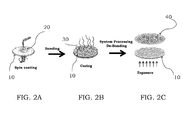
- the figures 2A-2C show the steps of a manufacturing method comprising a step of releasing the carrier based on the laser ablation technique. More in details, as shown in figure 2A , a transparent carrier 10, like quartz, is provided and a liquid plastic precursor 20, such as polyimide, is spun on the carrier 10; the plastic precursor 20 is then cured to form a plastic substrate 30 bonded to the carrier 10. The carrier 10 with the plastic substrate 30 fixed to it is showed in figure 2B . At the end, an electronic device 40 is realized over the plastic substrate 30 and then released from the carrier 10 exposing it to a laser light at ultraviolet wavelengths to cause the lift-off.
- a transparent carrier 10 like quartz
- a liquid plastic precursor 20 such as polyimide
- the transparent carrier substrates such as quartz, are very expensive.
- the technical problem of the present invention is that of providing a carrier for an electronic device to be realized on a plastic substrate and a method of manufacturing an electronic device having plastic substrate having structural and functional characteristics allowing to overcome the limits which still affect the carriers and the methods previously disclosed with reference to the prior art.
- the solution idea underlying the present invention is that of method of manufacturing an electronic device providing a special carrier for supporting a plastic substrate whereon realizing an electronic device, such a carrier being provided with a metallic layer in contact with the plastic substrate, the metallic layer being able to guarantee a temporarily bonding of the plastic substrate on the carrier, being released immerging the electronic device bonded to the carrier in a solution of hydrogen peroxide (H 2 O 2 ) which breaks the bonds between the plastic substrate and the metallic layer.
- H 2 O 2 hydrogen peroxide
- the metallic layer may be a double layer in the case of carriers that need an adhesion layer between the carrier itself and the metallic layer on which the plastic substrate is supported.
- the invention comprises the following supplemental and optional features, taken alone or in combination when needed.
- the solution hydrogen peroxide (H 2 O 2 ) may be at room temperature.
- the solution of hydrogen peroxide may be in percentage comprised in the range of 10-50%, and preferably at 30%.
- the step of providing the carrier may comprise the steps of:
- the step of releasing the carrier may comprise forming a protective tape on the electronic device.
- the step of providing a substrate may comprise a step of providing a wafer or a die.
- the step of providing a substrate may comprise providing a layer made by silicon or glass.
- step of providing the metallic layer may comprise a step of providing a layer made of Platinum (Pt) or Palladium (Pd).
- step of providing the metallic layer may comprise a step of providing a double layer comprising an adhesion promoter including: Ti, TiN.
- the thickness of the metallic layer may be in the range of 50-150nm.
- a carrier 100 acting as a rigid support for an electronic device having a plastic substrate.
- the carrier 100 comprises a rigid substrate 101, and a metallic layer 102.
- the substrate 101 may be a silicon wafer or any other alternative wafer structure normally used in the microelectronic field.
- the metallic layer 102 may be a double layer comprising a further metallic layer acting as an adhesion promoter between the carrier and the metallic layer itself, when needed.
- the substrate 101 may be a die.
- the substrate 101 may be either a silicon substrate or a glass substrate or another material having features, such as shape, weight and dimensions, similar to silicon or glass.
- the metallic layer 102 is deposited on the substrate 101 to guarantee a temporarily bonding of the substrate, in particular a plastic substrate, on the carrier 100.
- the metallic layer 102 is a Platinum (Pt) layer.
- the metallic layer 102 is a Palladium (Pd) layer.
- every kind of material having properties of good adhesion to the substrate 101 can be used as a further layer of the double metallic layer 102, in particular comprising an adhesion promoter including: Ti, TiN.
- every kind of material having the same properties of temporarily bonding a plastic substrate on the carrier 100 can be used as metallic layer 102.
- the thickness of the metallic layer 102 is in the range of 50-200nm in order to allow saving the cost of the carrier and to re-use it for future processes, as will be cleared in the following with reference to the manufacturing method according to the invention.
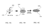
- Figure 4A shows a rigid carrier 100 covered by a liquid plastic precursor 200, such as polyimide, and subjected to a spread out diffusion by means of a spin coating phase.
- a liquid plastic precursor 200 such as polyimide
- the polyimide is cured to form a plastic substrate 300 which is bonded to the rigid carrier 100, as shown in figure 4B .
- the plastic substrate 300 is then subjected to standard process steps driving to the manufacture of electronic devices 400, as shown in figure 4C , having the plastic substrate 300 fixed to the rigid carrier 100.
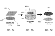
- FIG 5A it is shown an electronic device 400 covered by a protective thermal releasable tape 404, simultaneously protecting the device from damages and from rolling up.
- the electronic device 400 covered with the protective tape 404 is then released by the rigid substrate 100 thanks to a removal phase breaking the bonds between the plastic substrate 300 and the metallic layer 102.
- the whole electronic device 400 may be immerged in a hydrogen peroxide (H 2 O 2 ) 30% solution at room temperature, as shown in figure 5B , to allow the breaking of said bonds and thus the de-bonding of the electronic device 400 from the rigid carrier 100.
- H 2 O 2 hydrogen peroxide
- Figure 5C shows a schematic view of the electronic device 400 separated both from the carrier 100 and also from the protective tape 404.
- the present application also relates to a method for manufacturing an electronic device 400 having a plastic substrate 300, the method comprising the steps of:
- One of the most important aspects of the present invention is the possibility offered by the presence of the metal layer 102 on the carrier 100 to act as a temporary bonding of the plastic substrate 300. For instance the spin coating phase may be missing if a plastic substrate should be already available for a bonding of the metal layer 102.
- the oxygenated water solution is a hydrogen peroxide (H 2 O 2 ) 30% solution at room temperature.
- the oxygenated water solution is a solution of hydrogen peroxide (H 2 O 2 ) in percentage comprised in the range of 10-50%, and preferably at 30%.
- the electronic device 400 immerged in the described solution is subject, due to the catalyst activity of the metallic layer 102, to the H 2 O 2 dismutation reaction: 2H 2 O 2 ⁇ 2H 2 O+O 2g
- the gaseous oxygen (O 2g ) obtained from the reaction is able to break the bonds between the polyimide of the plastic substrate 200 and the platinum of the metallic layer 102.
- Another advantage relates to the simply and economic manufacturing process being implemented and to the possibility of re-using the carrier, thus reducing the fabrication costs.
- the process is not invasive for the electronic devices having a flexible substrate so obtained.
Landscapes
- Engineering & Computer Science (AREA)
- Manufacturing & Machinery (AREA)
- Microelectronics & Electronic Packaging (AREA)
- Thin Film Transistor (AREA)
- Encapsulation Of And Coatings For Semiconductor Or Solid State Devices (AREA)
Abstract
Description
- The present invention relates to a method of manufacturing an electronic device realized on plastic substrates, such as active matrix display devices or photovoltaic panels or sensors network.
- The invention refers, in particular, but not exclusively, to a method of manufacturing an electronic device comprising a plastic substrate fixed to a rigid carrier, and the following description is made with reference to this field of application just for explanation convenience.
- Recently, interest in plastic devices for displays, photovoltaic panels and sensor networks has increased even further, due to the low cost, the light weight, the flexibility and the resistance to broken. Despite this interest, there is still a need for a plausible manufacturing route for mass production of this kind of devices.
- A number of different ways have been reported for the manufacturing of electronic devices on plastic substrates; however, all these manufacturing ways have some drawbacks mainly due to:
- the difficulty of setting-up processes compatible with plastics which require low temperatures and non aggressive chemicals;
- managing of flexible, light and sometimes transparent devices using conventional equipments generally suitable for processing rigid substrates.
- It is well known that a possibility for manufacturing flexible devices using conventional equipments is to process a plastic substrate fixed over a rigid carrier substrate. The rigid carrier substrate is then released from the plastic substrate after having formed the circuit layouts over the plastic substrate. This enables to employ substantially conventional substrate handling and cell making processes. This known technique is called "temporary bonding" because it consists in fixing the plastic substrate on the rigid substrate, also called the carrier, for a limited time period and in removing the plastic substrate from the carrier at the end of the manufacturing process.
- As an example,
figures 1A-1C show the steps of a manufacturing process of an electronic device having a plastic substrate, according to the prior art. In particular,figure 1A shows arigid carrier 1 and aplastic foil 2 that can be cut, modelled and bonded on thecarrier 1, thus covering it as aplastic substrate 3 as shown infigure 1B. Figure 1C shows anelectronic device 4 manufactured on theplastic substrate 3 then released from thecarrier 1. - Several methods are used to release the carrier from the plastic substrate at the end of the manufacturing process, depending on the plastic materials being used. In particular, a first type of plastic materials, such as PEN, PET, Arilite, Kapton, etc., can be laminated on the carrier. A second type of plastic materials can be obtained from liquid precursors, such as polyimide, silicon pastes, etc., which are deposited on the carrier, as they are or covered by either a metal or oxide or nitride layer, and then cured at high temperatures.
- For the first type of plastic materials, a first known manufacturing process involves the steps of:
- laminating a double-sided tape on the carrier; laminating the plastic materials on the double-sided tape;
- realizing the electronic device on the plastic material;
- releasing the carrier from the plastic substrate, putting it over a hot plate increasing its temperature.
- Even if the double-sided tapes are very resistant to chemical agents being used in manufacturing processes and even if they do not release any impurity both on the plastic substrate and on the carrier, allowing the re-use of the carrier, they are however low resistant to temperatures greater than 150°C, whereat an anticipated de-bonding of the carrier occurs.
- A second known manufacturing process involves the steps of:
- depositing a liquid glue on the carrier;
- laminating the plastic materials on the carrier;
- realizing the electronic device on the plastic material;
- releasing the carrier by means of a mechanical peeling on the plastic substrate or of a chemical remover of the glue.
- Although the glue is more resistant to high temperatures, up to 200°C, it could be easily damaged by the chemical substances used in device manufacturing processes. Moreover, the de-bonding may cause damaging of the electronic device already formed, either in case of a mechanical de-bonding or a chemical attack.
- A third known manufacturing process involves the steps of:
- providing an electrostatic carrier comprising a pair of electrodes on which a dielectric material is deposited;
- providing a plastic substrate adhering to the carrier due to the electrostatic field formed on it by an external power supply;
- realizing the electronic device on the plastic material;
- moving away the device from the carrier.
- The advantage of this technique is to avoid the surface contamination determined by glue or by adhesive tapes, so that the carrier can be re-used for producing standard devices in semiconductor industries. Nevertheless, the electrostatic field exponentially decreases with time and is very sensitive to thermal processes, causing the anticipated de-bonding of the carrier.
- For the second type of plastic materials, a first known manufacturing process involves the steps of:
- providing a carrier with a superficial sacrificial layer;
- spinning a liquid precursor on the carrier, in such a way to adhere to the sacrificial layer;
- curing the precursor to form a thin film;
- realizing the electronic device on the thin film;
- removing the carrier by means of a wet etch or of an anodic dissolution.
- The biggest problem of this type of de-bonding is that the carrier cannot be re-used. Moreover, in case of wet etch, the diffusion velocity of the removing solution is very limited, so that, for devices having an area of cm2, the duration period of the wet etch could cause damaging of the devices. This is way the wet etch is more applicable for small devices and for carriers having a big area exposed to the removing solution. Similarly, the de-bonding by anodic dissolution involves a more rapid corrosion of the metals of the carrier exposed to the anodic solution as much as greater is the area of the exposed metals. In addition, this type of de-bonding cannot be used if the plastic substrate covers completely the sacrificial layer and it requests the use of a dedicated equipment to control the parameters of the dissolution process.
- There is another known manufacturing process, specifically used for liquid photosensitive precursors, such as polyimide, and for transparent carriers involving the steps of:
- spinning a liquid precursor on the carrier;
- curing the precursor to form a thin film;
- realizing the electronic device on the thin film;
- de-bonding the carrier by exposing the thin film to a laser having a specific wavelength, such as 308 nm (Xe-Cl) or 193 nm (ArF excimer laser), in such a way to ablate a sub-micrometric layer of the thin film which remains bonded to the carrier and to have the device on the plastic substrate de-bonded.
- For example, this last technique is described in the International patent application published under No.
WO 05/050754 on June 2, 2005 - The
figures 2A-2C show the steps of a manufacturing method comprising a step of releasing the carrier based on the laser ablation technique. More in details, as shown infigure 2A , atransparent carrier 10, like quartz, is provided and a liquidplastic precursor 20, such as polyimide, is spun on thecarrier 10; theplastic precursor 20 is then cured to form aplastic substrate 30 bonded to thecarrier 10. Thecarrier 10 with theplastic substrate 30 fixed to it is showed infigure 2B . At the end, anelectronic device 40 is realized over theplastic substrate 30 and then released from thecarrier 10 exposing it to a laser light at ultraviolet wavelengths to cause the lift-off. - There are some problems in using a heating effect to lift-off a plastic substrate from the glass. Sufficient energy is needed to enable lift off to occur, but without damaging either the plastic substrate or the components formed, damages occurring for the thermal expansion effects. When using a laser lift-off process, higher wavelengths within the UV spectrum are preferable because lower wavelengths are more absorbed by the glass substrate, making the laser release less effective. For example commercially available lasers which operate at 308nm or 351 nm are preferred. At these high wavelengths, the energy absorbed in the plastic layer is statistically distributed without complete thermalisation in the plastic polymer molecules. This gives rise to localized heating effects, which can in turn result in damages to the plastic substrate or the components mounted on it. This can also results in partial or poor lift-off from the carrier.
- Moreover, the transparent carrier substrates, such as quartz, are very expensive.
- The technical problem of the present invention is that of providing a carrier for an electronic device to be realized on a plastic substrate and a method of manufacturing an electronic device having plastic substrate having structural and functional characteristics allowing to overcome the limits which still affect the carriers and the methods previously disclosed with reference to the prior art.
- The solution idea underlying the present invention is that of method of manufacturing an electronic device providing a special carrier for supporting a plastic substrate whereon realizing an electronic device, such a carrier being provided with a metallic layer in contact with the plastic substrate, the metallic layer being able to guarantee a temporarily bonding of the plastic substrate on the carrier, being released immerging the electronic device bonded to the carrier in a solution of hydrogen peroxide (H2O2) which breaks the bonds between the plastic substrate and the metallic layer.
- More in particular, the metallic layer may be a double layer in the case of carriers that need an adhesion layer between the carrier itself and the metallic layer on which the plastic substrate is supported.
- On the basis of such solution idea the technical problem is solved by a method of manufacturing an electronic device having a plastic substrate, the method comprising the steps of:
- providing a carrier as a rigid support for the electronic device;
- providing at least a metallic layer on the carrier to guarantee a temporarily bonding of the plastic substrate on the carrier;
- providing a plastic substrate on the metallic layer;
- forming an electronic device over the plastic substrate;
- releasing the carrier from the plastic substrate;
- More in particular, the invention comprises the following supplemental and optional features, taken alone or in combination when needed.
- According to an aspect of the invention, the solution hydrogen peroxide (H2O2)may be at room temperature.
- Alternatively, the solution of hydrogen peroxide (H2O2) may be in percentage comprised in the range of 10-50%, and preferably at 30%.
- According to another aspect of the invention, the step of providing the carrier may comprise the steps of:
- providing a substrate;
- depositing the at least a metallic layer on the substrate. Moreover, the step of forming a plastic substrate on the metallic layer may comprise the steps of:
- spin coating a liquid plastic precursor on the metallic layer;
- curing the plastic precursor forming the plastic substrate.
- According to yet another aspect of the invention, the step of releasing the carrier may comprise forming a protective tape on the electronic device.
- According to an aspect of the invention, the step of providing a substrate may comprise a step of providing a wafer or a die. Moreover, the step of providing a substrate may comprise providing a layer made by silicon or glass.
- According to another aspect of the invention, step of providing the metallic layer may comprise a step of providing a layer made of Platinum (Pt) or Palladium (Pd).
- Moreover, step of providing the metallic layer may comprise a step of providing a double layer comprising an adhesion promoter including: Ti, TiN. The thickness of the metallic layer may be in the range of 50-150nm.
- The characteristics and advantages of the manufacturing method according to the present invention will be apparent from the following description of an embodiment thereof given by way of indicative and non limiting example with reference to the annexed drawings.
- In such drawings:
-
Figures 1A-1C schematically show the steps of a manufacturing process of an electronic device having a plastic substrate, according to the prior art; -
Figures 2A-2C schematically show the steps of a manufacturing process of an electronic device having a plastic substrate comprising a step of releasing the carrier based on laser ablation, according to the prior art; -
Figure 3 schematically shows a cross section of a carrier, being realised by a manufacturing method according to the invention; -
Figures 4A-4C schematically show the steps of a manufacturing process of an electronic device having a plastic substrate on a carrier, being realised according to the invention; and -
Figures 5A-5C schematically show the steps of the manufacturing process of an electronic device having a plastic substrate comprising a de-bonding of the carrier, being realised according to the invention. - With reference to such figures, and in particular to
Figure 3 , acarrier 100 is shown acting as a rigid support for an electronic device having a plastic substrate. - In particular, the
carrier 100 comprises arigid substrate 101, and ametallic layer 102. - According to an aspect of the invention, the
substrate 101 may be a silicon wafer or any other alternative wafer structure normally used in the microelectronic field. Themetallic layer 102 may be a double layer comprising a further metallic layer acting as an adhesion promoter between the carrier and the metallic layer itself, when needed. - According to another aspect of the invention, the
substrate 101 may be a die. - Moreover, the
substrate 101 may be either a silicon substrate or a glass substrate or another material having features, such as shape, weight and dimensions, similar to silicon or glass. - The
metallic layer 102 is deposited on thesubstrate 101 to guarantee a temporarily bonding of the substrate, in particular a plastic substrate, on thecarrier 100. - According to an aspect of the invention, the
metallic layer 102 is a Platinum (Pt) layer. - According to another aspect of the invention, the
metallic layer 102 is a Palladium (Pd) layer. - According to an aspect of the invention, when a double metallic layer is used, every kind of material having properties of good adhesion to the
substrate 101 can be used as a further layer of the doublemetallic layer 102, in particular comprising an adhesion promoter including: Ti, TiN. - According to another aspect of the invention, every kind of material having the same properties of temporarily bonding a plastic substrate on the
carrier 100 can be used asmetallic layer 102. - The thickness of the
metallic layer 102 is in the range of 50-200nm in order to allow saving the cost of the carrier and to re-use it for future processes, as will be cleared in the following with reference to the manufacturing method according to the invention. -
Figure 4A shows arigid carrier 100 covered by a liquidplastic precursor 200, such as polyimide, and subjected to a spread out diffusion by means of a spin coating phase. - After that, the polyimide is cured to form a
plastic substrate 300 which is bonded to therigid carrier 100, as shown infigure 4B . Theplastic substrate 300 is then subjected to standard process steps driving to the manufacture ofelectronic devices 400, as shown infigure 4C , having theplastic substrate 300 fixed to therigid carrier 100. - According to an aspect of the invention, in
figure 5A it is shown anelectronic device 400 covered by a protective thermalreleasable tape 404, simultaneously protecting the device from damages and from rolling up. Theelectronic device 400 covered with theprotective tape 404 is then released by therigid substrate 100 thanks to a removal phase breaking the bonds between theplastic substrate 300 and themetallic layer 102. For instance, the wholeelectronic device 400 may be immerged in a hydrogen peroxide (H2O2) 30% solution at room temperature, as shown infigure 5B , to allow the breaking of said bonds and thus the de-bonding of theelectronic device 400 from therigid carrier 100. -
Figure 5C shows a schematic view of theelectronic device 400 separated both from thecarrier 100 and also from theprotective tape 404. - As already explained, the present application also relates to a method for manufacturing an
electronic device 400 having aplastic substrate 300, the method comprising the steps of: - providing a
carrier 100 able to act as a rigid support for theelectronic device 400; - spin coating the
carrier 100 with a liquidplastic precursor 200; - curing the
plastic precursor 200, obtaining aplastic substrate 300; - cleaning the surface of the
plastic substrate 300; - fabricating the desired electronic device;
- depositing a
protective tape 404 over theelectronic device 400; and - releasing the
plastic substrate 300 from thecarrier 100 by immerging theelectronic device 400 covered with theprotective tape 404 in a solution able to produce the separation of thecarrier 100; for instance an oxygenated water solution. - As a skilled person in the art may appreciate, not all the above phases are strictly necessary for obtaining the final result of the
electronic device 400 free from thecarrier 100. - One of the most important aspects of the present invention is the possibility offered by the presence of the
metal layer 102 on thecarrier 100 to act as a temporary bonding of theplastic substrate 300. For instance the spin coating phase may be missing if a plastic substrate should be already available for a bonding of themetal layer 102. - The manufacturing method further advantageously comprises the steps of:
- providing the
carrier 100 comprising arigid substrate 101 and ametallic layer 102; and - realising the
protective tape 404 for theelectronic device 400 by means of a thermal process. - Advantageously, according to an aspect of the invention, the oxygenated water solution is a hydrogen peroxide (H2O2) 30% solution at room temperature.
- Advantageously, according to another aspect of the invention, the oxygenated water solution is a solution of hydrogen peroxide (H2O2) in percentage comprised in the range of 10-50%, and preferably at 30%.
- More in details, the
electronic device 400 immerged in the described solution, is subject, due to the catalyst activity of themetallic layer 102, to the H2O2 dismutation reaction:
2H2O2 → 2H2O+O2g
- The gaseous oxygen (O2g) obtained from the reaction is able to break the bonds between the polyimide of the
plastic substrate 200 and the platinum of themetallic layer 102. - The separation is very fast, in the order of few minutes (1-5min) for a wafer of 15.24cm (6") immerged in 100 ml of solution.
- The advantages that described carrier for an electronic device having a plastic substrate and of the corresponding manufacturing method of the electronic device having plastic substrate emerge clearly from the foregoing discussion.
- In particular, advantageously according to the present invention, no need is felt of having specific equipments, such as laser sources, to realize the releasing of the carrier from the electronic device having a plastic substrate.
- In addition, advantageously according to the invention, it is possible to simultaneously and quickly process multiple wafers acting as rigid supports of electronic devices having a plastic substrate.
- Another advantage relates to the simply and economic manufacturing process being implemented and to the possibility of re-using the carrier, thus reducing the fabrication costs.
- Moreover, the process is not invasive for the electronic devices having a flexible substrate so obtained.
- Obviously, a technician of the field, aiming at meeting incidental and specific needs, will bring several modifications to the above described method, all within the scope of protection of the invention as defined by the following claims.
Claims (11)
- A method of manufacturing an electronic device (400) having a plastic substrate (200), the method comprising the steps of:- providing a carrier (100) as a rigid support for said electronic device (400);- providing at least a metallic layer (102) on the carrier (100) to guarantee a temporarily bonding of said plastic substrate (200) on said carrier (100);- providing a plastic substrate (300) on said metallic layer (102);- forming an electronic device (400) over said plastic substrate (300);- releasing said carrier (100) from said plastic substrate (300);characterized in that said step of releasing said carrier (100) comprising immerging said electronic device (400) bonded to said carrier (100) in a solution of hydrogen peroxide (H2O2) breaking the bonds between said plastic substrate (300) and said metallic layer (102).
- A method according to claim 1, wherein said solution of hydrogen peroxide (H2O2) is at room temperature.
- A method according to claim 1, wherein said solution of hydrogen peroxide (H2O2) is in percentage comprised in the range of 10-50%, and preferably at 30%.
- A method according to claim 1, wherein said step of providing said carrier (100) comprises the steps of:- providing a substrate (101);- depositing said at least a metallic layer (102) on said substrate (101).
- A method according to claim 1, wherein said step of forming a plastic substrate (300) on said metallic layer (102) comprises the steps of:- spin coating a liquid plastic precursor (200) on said metallic layer (102);- curing said plastic precursor (200) forming said plastic substrate (300).
- A method according to claim 1, wherein said step of releasing said carrier (100) comprises forming a protective tape (404) on said electronic device (400).
- A method according to claim 2, wherein said step of providing a substrate (101)comprises a step of providing a wafer or a die.
- A method according to claim 2, wherein said step of providing a substrate (101) comprises a step of providing a layer made by:- silicon; or- glass.
- A method according to claim 1, wherein said step of providing said metallic layer (102) comprises a step of providing a layer made of:- Platinum (Pt); or- Palladium (Pd).
- A method according to claim 1, wherein said step of providing said metallic layer (102) comprises a step of providing a double layer comprising an adhesion promoter including: Ti, TiN.
- A method according to claim 1, wherein said step of providing said metallic layer (102) comprises a step of providing a layer having a thickness in the range of 50-150nm.
Applications Claiming Priority (1)
| Application Number | Priority Date | Filing Date | Title |
|---|---|---|---|
| ITMI20111405 | 2011-07-27 |
Publications (2)
| Publication Number | Publication Date |
|---|---|
| EP2551895A1 true EP2551895A1 (en) | 2013-01-30 |
| EP2551895B1 EP2551895B1 (en) | 2013-11-27 |
Family
ID=44675684
Family Applications (1)
| Application Number | Title | Priority Date | Filing Date |
|---|---|---|---|
| EP12169044.0A Not-in-force EP2551895B1 (en) | 2011-07-27 | 2012-05-23 | Method of manufacturing an electronic device having a plastic substrate |
Country Status (2)
| Country | Link |
|---|---|
| US (1) | US8575005B2 (en) |
| EP (1) | EP2551895B1 (en) |
Families Citing this family (4)
| Publication number | Priority date | Publication date | Assignee | Title |
|---|---|---|---|---|
| CN103682177B (en) * | 2013-12-16 | 2015-03-25 | 深圳市华星光电技术有限公司 | Manufacturing method of flexible OLED panel |
| KR102327141B1 (en) | 2014-11-19 | 2021-11-16 | 삼성전자주식회사 | Pre-package and manufacturing method of semiconductor package using the same |
| US10570011B1 (en) * | 2018-08-30 | 2020-02-25 | United States Of America As Represented By Secretary Of The Navy | Method and system for fabricating a microelectromechanical system device with a movable portion using anodic etching of a sacrificial layer |
| WO2025085890A2 (en) * | 2023-10-19 | 2025-04-24 | Brewer Science, Inc. | Versatile dual-layer temporary wafer bonding for harsh processing conditions |
Citations (6)
| Publication number | Priority date | Publication date | Assignee | Title |
|---|---|---|---|---|
| US5151388A (en) * | 1991-05-07 | 1992-09-29 | Hughes Aircraft Company | Flip interconnect |
| WO2005050754A1 (en) | 2003-11-21 | 2005-06-02 | Koninklijke Philips Electronics N.V. | Active matrix displays and other electronic devices having plastic substrates |
| WO2008018026A2 (en) * | 2006-08-10 | 2008-02-14 | Koninklijke Philips Electronics N.V. | Active matrix displays and other electronic devices having plastic substrates |
| EP2022626A2 (en) * | 2007-07-19 | 2009-02-11 | Samsung SDI Co., Ltd. | Method of joining and method of fabricating an organic light emitting diode display device using the same |
| US20090305467A1 (en) * | 2008-06-06 | 2009-12-10 | Semiconductor Energy Laboratory Co., Ltd. | Method for manufacturing semiconductor device |
| US20090314527A1 (en) * | 2008-06-20 | 2009-12-24 | Semiconductor Energy Laboratory Co., Ltd. | Semiconductor device and manufacturing method thereof |
Family Cites Families (6)
| Publication number | Priority date | Publication date | Assignee | Title |
|---|---|---|---|---|
| EP1351308B1 (en) | 1996-08-27 | 2009-04-22 | Seiko Epson Corporation | Exfoliating method and transferring method of thin film device |
| US5972152A (en) | 1997-05-16 | 1999-10-26 | Micron Communications, Inc. | Methods of fixturing flexible circuit substrates and a processing carrier, processing a flexible circuit and processing a flexible circuit substrate relative to a processing carrier |
| US7226812B2 (en) | 2004-03-31 | 2007-06-05 | Intel Corporation | Wafer support and release in wafer processing |
| US8137417B2 (en) | 2006-09-29 | 2012-03-20 | Semiconductor Energy Laboratory Co., Ltd. | Peeling apparatus and manufacturing apparatus of semiconductor device |
| US7989022B2 (en) | 2007-07-20 | 2011-08-02 | Micron Technology, Inc. | Methods of processing substrates, electrostatic carriers for retaining substrates for processing, and assemblies comprising electrostatic carriers having substrates electrostatically bonded thereto |
| JP5620921B2 (en) | 2008-12-05 | 2014-11-05 | コーニンクレッカ フィリップス エヌ ヴェ | Electronic device having plastic substrate and manufacturing method thereof |
-
2012
- 2012-05-23 EP EP12169044.0A patent/EP2551895B1/en not_active Not-in-force
- 2012-07-26 US US13/559,433 patent/US8575005B2/en not_active Expired - Fee Related
Patent Citations (6)
| Publication number | Priority date | Publication date | Assignee | Title |
|---|---|---|---|---|
| US5151388A (en) * | 1991-05-07 | 1992-09-29 | Hughes Aircraft Company | Flip interconnect |
| WO2005050754A1 (en) | 2003-11-21 | 2005-06-02 | Koninklijke Philips Electronics N.V. | Active matrix displays and other electronic devices having plastic substrates |
| WO2008018026A2 (en) * | 2006-08-10 | 2008-02-14 | Koninklijke Philips Electronics N.V. | Active matrix displays and other electronic devices having plastic substrates |
| EP2022626A2 (en) * | 2007-07-19 | 2009-02-11 | Samsung SDI Co., Ltd. | Method of joining and method of fabricating an organic light emitting diode display device using the same |
| US20090305467A1 (en) * | 2008-06-06 | 2009-12-10 | Semiconductor Energy Laboratory Co., Ltd. | Method for manufacturing semiconductor device |
| US20090314527A1 (en) * | 2008-06-20 | 2009-12-24 | Semiconductor Energy Laboratory Co., Ltd. | Semiconductor device and manufacturing method thereof |
Also Published As
| Publication number | Publication date |
|---|---|
| EP2551895B1 (en) | 2013-11-27 |
| US20130029486A1 (en) | 2013-01-31 |
| US8575005B2 (en) | 2013-11-05 |
Similar Documents
| Publication | Publication Date | Title |
|---|---|---|
| US12398066B2 (en) | Method for producing a display having a carrier substrate, a carrier substrate produced according to said method, and a cover glass intended for a flexible display | |
| US10490315B2 (en) | Method for obtaining multilayer graphene | |
| TWI862574B (en) | Systems and methods for manufacturing flexible electronics | |
| US8871609B2 (en) | Thin wafer handling structure and method | |
| TWI446420B (en) | Carrier separation method for semiconductor process | |
| CN103682176B (en) | The manufacture method of rigid substrate substrate and flexible display device, rigid substrate substrate | |
| KR20100027526A (en) | Fabrication method of thin film device | |
| CN102653663A (en) | Tackiness adhesive sheet for thin-film substrate fixing | |
| JP2006237011A (en) | Method and material for manufacturing flexible circuit structure | |
| TW201033000A (en) | Glass laminate and manufacturing method therefor | |
| EP2551895B1 (en) | Method of manufacturing an electronic device having a plastic substrate | |
| CN106663640A (en) | Method for providing electronic device and electronic device thereof | |
| JP5898949B2 (en) | Method for manufacturing flexible device | |
| CN105789116A (en) | Manufacturing method of flexible substrate | |
| JP5931067B2 (en) | Board sheet | |
| TWI895518B (en) | Techniques for fabricating and separating flexible microelectronics devices from rigid substrates | |
| JP2015532004A (en) | Flexible glass substrate processing | |
| JP2013009016A (en) | Manufacturing method of integrated thin film element | |
| JP2010062526A (en) | Method of manufacturing thin film element | |
| TW201139153A (en) | Method for eliminating resin film and method for producing laminate | |
| US10305147B2 (en) | Method for reversible bonding between two elements | |
| JP2005078064A (en) | Manufacturing method of flexible panel | |
| JP2009231533A (en) | Peeling method, peeling apparatus and method of manufacturing semiconductor device | |
| US8747598B2 (en) | Method of forming a permanently supported lamina | |
| KR101920144B1 (en) | Flexible substrate for flexible electronic device, method of fabricating flexible electronic device using the same, and flexible electronic device fabriacated by the method |
Legal Events
| Date | Code | Title | Description |
|---|---|---|---|
| PUAI | Public reference made under article 153(3) epc to a published international application that has entered the european phase |
Free format text: ORIGINAL CODE: 0009012 |
|
| AK | Designated contracting states |
Kind code of ref document: A1 Designated state(s): AL AT BE BG CH CY CZ DE DK EE ES FI FR GB GR HR HU IE IS IT LI LT LU LV MC MK MT NL NO PL PT RO RS SE SI SK SM TR |
|
| AX | Request for extension of the european patent |
Extension state: BA ME |
|
| 17P | Request for examination filed |
Effective date: 20130528 |
|
| RBV | Designated contracting states (corrected) |
Designated state(s): AL AT BE BG CH CY CZ DE DK EE ES FI FR GB GR HR HU IE IS IT LI LT LU LV MC MK MT NL NO PL PT RO RS SE SI SK SM TR |
|
| RIC1 | Information provided on ipc code assigned before grant |
Ipc: H01L 51/00 20060101ALN20130619BHEP Ipc: H01L 21/683 20060101AFI20130619BHEP Ipc: H01L 27/12 20060101ALN20130619BHEP |
|
| GRAP | Despatch of communication of intention to grant a patent |
Free format text: ORIGINAL CODE: EPIDOSNIGR1 |
|
| RIC1 | Information provided on ipc code assigned before grant |
Ipc: H01L 21/683 20060101AFI20130722BHEP Ipc: H01L 27/12 20060101ALN20130722BHEP Ipc: H01L 51/00 20060101ALN20130722BHEP |
|
| INTG | Intention to grant announced |
Effective date: 20130823 |
|
| GRAS | Grant fee paid |
Free format text: ORIGINAL CODE: EPIDOSNIGR3 |
|
| GRAA | (expected) grant |
Free format text: ORIGINAL CODE: 0009210 |
|
| AK | Designated contracting states |
Kind code of ref document: B1 Designated state(s): AL AT BE BG CH CY CZ DE DK EE ES FI FR GB GR HR HU IE IS IT LI LT LU LV MC MK MT NL NO PL PT RO RS SE SI SK SM TR |
|
| REG | Reference to a national code |
Ref country code: GB Ref legal event code: FG4D |
|
| REG | Reference to a national code |
Ref country code: CH Ref legal event code: EP |
|
| REG | Reference to a national code |
Ref country code: AT Ref legal event code: REF Ref document number: 643012 Country of ref document: AT Kind code of ref document: T Effective date: 20131215 |
|
| REG | Reference to a national code |
Ref country code: IE Ref legal event code: FG4D |
|
| REG | Reference to a national code |
Ref country code: DE Ref legal event code: R096 Ref document number: 602012000582 Country of ref document: DE Effective date: 20140123 |
|
| REG | Reference to a national code |
Ref country code: NL Ref legal event code: VDEP Effective date: 20131127 |
|
| REG | Reference to a national code |
Ref country code: AT Ref legal event code: MK05 Ref document number: 643012 Country of ref document: AT Kind code of ref document: T Effective date: 20131127 |
|
| REG | Reference to a national code |
Ref country code: LT Ref legal event code: MG4D |
|
| PG25 | Lapsed in a contracting state [announced via postgrant information from national office to epo] |
Ref country code: LT Free format text: LAPSE BECAUSE OF FAILURE TO SUBMIT A TRANSLATION OF THE DESCRIPTION OR TO PAY THE FEE WITHIN THE PRESCRIBED TIME-LIMIT Effective date: 20131127 Ref country code: HR Free format text: LAPSE BECAUSE OF FAILURE TO SUBMIT A TRANSLATION OF THE DESCRIPTION OR TO PAY THE FEE WITHIN THE PRESCRIBED TIME-LIMIT Effective date: 20131127 Ref country code: FI Free format text: LAPSE BECAUSE OF FAILURE TO SUBMIT A TRANSLATION OF THE DESCRIPTION OR TO PAY THE FEE WITHIN THE PRESCRIBED TIME-LIMIT Effective date: 20131127 Ref country code: NL Free format text: LAPSE BECAUSE OF FAILURE TO SUBMIT A TRANSLATION OF THE DESCRIPTION OR TO PAY THE FEE WITHIN THE PRESCRIBED TIME-LIMIT Effective date: 20131127 Ref country code: NO Free format text: LAPSE BECAUSE OF FAILURE TO SUBMIT A TRANSLATION OF THE DESCRIPTION OR TO PAY THE FEE WITHIN THE PRESCRIBED TIME-LIMIT Effective date: 20140227 Ref country code: SE Free format text: LAPSE BECAUSE OF FAILURE TO SUBMIT A TRANSLATION OF THE DESCRIPTION OR TO PAY THE FEE WITHIN THE PRESCRIBED TIME-LIMIT Effective date: 20131127 Ref country code: IS Free format text: LAPSE BECAUSE OF FAILURE TO SUBMIT A TRANSLATION OF THE DESCRIPTION OR TO PAY THE FEE WITHIN THE PRESCRIBED TIME-LIMIT Effective date: 20140327 |
|
| PG25 | Lapsed in a contracting state [announced via postgrant information from national office to epo] |
Ref country code: RS Free format text: LAPSE BECAUSE OF FAILURE TO SUBMIT A TRANSLATION OF THE DESCRIPTION OR TO PAY THE FEE WITHIN THE PRESCRIBED TIME-LIMIT Effective date: 20131127 Ref country code: LV Free format text: LAPSE BECAUSE OF FAILURE TO SUBMIT A TRANSLATION OF THE DESCRIPTION OR TO PAY THE FEE WITHIN THE PRESCRIBED TIME-LIMIT Effective date: 20131127 Ref country code: AT Free format text: LAPSE BECAUSE OF FAILURE TO SUBMIT A TRANSLATION OF THE DESCRIPTION OR TO PAY THE FEE WITHIN THE PRESCRIBED TIME-LIMIT Effective date: 20131127 Ref country code: ES Free format text: LAPSE BECAUSE OF FAILURE TO SUBMIT A TRANSLATION OF THE DESCRIPTION OR TO PAY THE FEE WITHIN THE PRESCRIBED TIME-LIMIT Effective date: 20131127 Ref country code: CY Free format text: LAPSE BECAUSE OF FAILURE TO SUBMIT A TRANSLATION OF THE DESCRIPTION OR TO PAY THE FEE WITHIN THE PRESCRIBED TIME-LIMIT Effective date: 20131127 Ref country code: BE Free format text: LAPSE BECAUSE OF FAILURE TO SUBMIT A TRANSLATION OF THE DESCRIPTION OR TO PAY THE FEE WITHIN THE PRESCRIBED TIME-LIMIT Effective date: 20131127 |
|
| PG25 | Lapsed in a contracting state [announced via postgrant information from national office to epo] |
Ref country code: PT Free format text: LAPSE BECAUSE OF FAILURE TO SUBMIT A TRANSLATION OF THE DESCRIPTION OR TO PAY THE FEE WITHIN THE PRESCRIBED TIME-LIMIT Effective date: 20140327 |
|
| PG25 | Lapsed in a contracting state [announced via postgrant information from national office to epo] |
Ref country code: EE Free format text: LAPSE BECAUSE OF FAILURE TO SUBMIT A TRANSLATION OF THE DESCRIPTION OR TO PAY THE FEE WITHIN THE PRESCRIBED TIME-LIMIT Effective date: 20131127 |
|
| REG | Reference to a national code |
Ref country code: DE Ref legal event code: R097 Ref document number: 602012000582 Country of ref document: DE |
|
| PG25 | Lapsed in a contracting state [announced via postgrant information from national office to epo] |
Ref country code: PL Free format text: LAPSE BECAUSE OF FAILURE TO SUBMIT A TRANSLATION OF THE DESCRIPTION OR TO PAY THE FEE WITHIN THE PRESCRIBED TIME-LIMIT Effective date: 20131127 Ref country code: RO Free format text: LAPSE BECAUSE OF FAILURE TO SUBMIT A TRANSLATION OF THE DESCRIPTION OR TO PAY THE FEE WITHIN THE PRESCRIBED TIME-LIMIT Effective date: 20131127 Ref country code: CZ Free format text: LAPSE BECAUSE OF FAILURE TO SUBMIT A TRANSLATION OF THE DESCRIPTION OR TO PAY THE FEE WITHIN THE PRESCRIBED TIME-LIMIT Effective date: 20131127 Ref country code: SK Free format text: LAPSE BECAUSE OF FAILURE TO SUBMIT A TRANSLATION OF THE DESCRIPTION OR TO PAY THE FEE WITHIN THE PRESCRIBED TIME-LIMIT Effective date: 20131127 |
|
| PG25 | Lapsed in a contracting state [announced via postgrant information from national office to epo] |
Ref country code: DK Free format text: LAPSE BECAUSE OF FAILURE TO SUBMIT A TRANSLATION OF THE DESCRIPTION OR TO PAY THE FEE WITHIN THE PRESCRIBED TIME-LIMIT Effective date: 20131127 |
|
| PLBE | No opposition filed within time limit |
Free format text: ORIGINAL CODE: 0009261 |
|
| STAA | Information on the status of an ep patent application or granted ep patent |
Free format text: STATUS: NO OPPOSITION FILED WITHIN TIME LIMIT |
|
| 26N | No opposition filed |
Effective date: 20140828 |
|
| REG | Reference to a national code |
Ref country code: DE Ref legal event code: R119 Ref document number: 602012000582 Country of ref document: DE |
|
| REG | Reference to a national code |
Ref country code: DE Ref legal event code: R097 Ref document number: 602012000582 Country of ref document: DE Effective date: 20140828 |
|
| PG25 | Lapsed in a contracting state [announced via postgrant information from national office to epo] |
Ref country code: LU Free format text: LAPSE BECAUSE OF FAILURE TO SUBMIT A TRANSLATION OF THE DESCRIPTION OR TO PAY THE FEE WITHIN THE PRESCRIBED TIME-LIMIT Effective date: 20140523 |
|
| PG25 | Lapsed in a contracting state [announced via postgrant information from national office to epo] |
Ref country code: MC Free format text: LAPSE BECAUSE OF FAILURE TO SUBMIT A TRANSLATION OF THE DESCRIPTION OR TO PAY THE FEE WITHIN THE PRESCRIBED TIME-LIMIT Effective date: 20131127 |
|
| REG | Reference to a national code |
Ref country code: IE Ref legal event code: MM4A |
|
| PG25 | Lapsed in a contracting state [announced via postgrant information from national office to epo] |
Ref country code: SI Free format text: LAPSE BECAUSE OF FAILURE TO SUBMIT A TRANSLATION OF THE DESCRIPTION OR TO PAY THE FEE WITHIN THE PRESCRIBED TIME-LIMIT Effective date: 20131127 |
|
| REG | Reference to a national code |
Ref country code: FR Ref legal event code: ST Effective date: 20150130 |
|
| REG | Reference to a national code |
Ref country code: DE Ref legal event code: R119 Ref document number: 602012000582 Country of ref document: DE Effective date: 20141202 |
|
| PG25 | Lapsed in a contracting state [announced via postgrant information from national office to epo] |
Ref country code: DE Free format text: LAPSE BECAUSE OF NON-PAYMENT OF DUE FEES Effective date: 20141202 Ref country code: IE Free format text: LAPSE BECAUSE OF NON-PAYMENT OF DUE FEES Effective date: 20140523 Ref country code: IT Free format text: LAPSE BECAUSE OF FAILURE TO SUBMIT A TRANSLATION OF THE DESCRIPTION OR TO PAY THE FEE WITHIN THE PRESCRIBED TIME-LIMIT Effective date: 20131127 |
|
| PG25 | Lapsed in a contracting state [announced via postgrant information from national office to epo] |
Ref country code: FR Free format text: LAPSE BECAUSE OF NON-PAYMENT OF DUE FEES Effective date: 20140602 |
|
| REG | Reference to a national code |
Ref country code: CH Ref legal event code: PL |
|
| PG25 | Lapsed in a contracting state [announced via postgrant information from national office to epo] |
Ref country code: CH Free format text: LAPSE BECAUSE OF NON-PAYMENT OF DUE FEES Effective date: 20150531 Ref country code: LI Free format text: LAPSE BECAUSE OF NON-PAYMENT OF DUE FEES Effective date: 20150531 |
|
| PG25 | Lapsed in a contracting state [announced via postgrant information from national office to epo] |
Ref country code: MT Free format text: LAPSE BECAUSE OF FAILURE TO SUBMIT A TRANSLATION OF THE DESCRIPTION OR TO PAY THE FEE WITHIN THE PRESCRIBED TIME-LIMIT Effective date: 20131127 |
|
| PG25 | Lapsed in a contracting state [announced via postgrant information from national office to epo] |
Ref country code: SM Free format text: LAPSE BECAUSE OF FAILURE TO SUBMIT A TRANSLATION OF THE DESCRIPTION OR TO PAY THE FEE WITHIN THE PRESCRIBED TIME-LIMIT Effective date: 20131127 |
|
| PG25 | Lapsed in a contracting state [announced via postgrant information from national office to epo] |
Ref country code: BG Free format text: LAPSE BECAUSE OF FAILURE TO SUBMIT A TRANSLATION OF THE DESCRIPTION OR TO PAY THE FEE WITHIN THE PRESCRIBED TIME-LIMIT Effective date: 20131127 Ref country code: GR Free format text: LAPSE BECAUSE OF FAILURE TO SUBMIT A TRANSLATION OF THE DESCRIPTION OR TO PAY THE FEE WITHIN THE PRESCRIBED TIME-LIMIT Effective date: 20140228 |
|
| PG25 | Lapsed in a contracting state [announced via postgrant information from national office to epo] |
Ref country code: HU Free format text: LAPSE BECAUSE OF FAILURE TO SUBMIT A TRANSLATION OF THE DESCRIPTION OR TO PAY THE FEE WITHIN THE PRESCRIBED TIME-LIMIT; INVALID AB INITIO Effective date: 20120523 Ref country code: TR Free format text: LAPSE BECAUSE OF FAILURE TO SUBMIT A TRANSLATION OF THE DESCRIPTION OR TO PAY THE FEE WITHIN THE PRESCRIBED TIME-LIMIT Effective date: 20131127 |
|
| GBPC | Gb: european patent ceased through non-payment of renewal fee |
Effective date: 20160523 |
|
| PG25 | Lapsed in a contracting state [announced via postgrant information from national office to epo] |
Ref country code: GB Free format text: LAPSE BECAUSE OF NON-PAYMENT OF DUE FEES Effective date: 20160523 |
|
| PG25 | Lapsed in a contracting state [announced via postgrant information from national office to epo] |
Ref country code: MK Free format text: LAPSE BECAUSE OF FAILURE TO SUBMIT A TRANSLATION OF THE DESCRIPTION OR TO PAY THE FEE WITHIN THE PRESCRIBED TIME-LIMIT Effective date: 20131127 |
|
| PG25 | Lapsed in a contracting state [announced via postgrant information from national office to epo] |
Ref country code: AL Free format text: LAPSE BECAUSE OF FAILURE TO SUBMIT A TRANSLATION OF THE DESCRIPTION OR TO PAY THE FEE WITHIN THE PRESCRIBED TIME-LIMIT Effective date: 20131127 |