EP2549468A1 - Display device with high frame rate capability - Google Patents
Display device with high frame rate capability Download PDFInfo
- Publication number
- EP2549468A1 EP2549468A1 EP11174606A EP11174606A EP2549468A1 EP 2549468 A1 EP2549468 A1 EP 2549468A1 EP 11174606 A EP11174606 A EP 11174606A EP 11174606 A EP11174606 A EP 11174606A EP 2549468 A1 EP2549468 A1 EP 2549468A1
- Authority
- EP
- European Patent Office
- Prior art keywords
- pixels
- horizontal lines
- display device
- scanning
- lines
- Prior art date
- Legal status (The legal status is an assumption and is not a legal conclusion. Google has not performed a legal analysis and makes no representation as to the accuracy of the status listed.)
- Withdrawn
Links
- 239000011159 matrix material Substances 0.000 claims abstract description 9
- 238000000034 method Methods 0.000 claims description 9
- 239000004973 liquid crystal related substance Substances 0.000 claims description 3
- 239000010409 thin film Substances 0.000 claims description 2
- 238000010586 diagram Methods 0.000 description 6
- 230000000694 effects Effects 0.000 description 6
- 238000010420 art technique Methods 0.000 description 2
- 238000005516 engineering process Methods 0.000 description 2
- 230000009286 beneficial effect Effects 0.000 description 1
- 239000003086 colorant Substances 0.000 description 1
- 238000004590 computer program Methods 0.000 description 1
- 230000001419 dependent effect Effects 0.000 description 1
- 238000003780 insertion Methods 0.000 description 1
- 230000037431 insertion Effects 0.000 description 1
- 230000003287 optical effect Effects 0.000 description 1
- 210000001525 retina Anatomy 0.000 description 1
Images


Classifications
-
- G—PHYSICS
- G09—EDUCATION; CRYPTOGRAPHY; DISPLAY; ADVERTISING; SEALS
- G09G—ARRANGEMENTS OR CIRCUITS FOR CONTROL OF INDICATING DEVICES USING STATIC MEANS TO PRESENT VARIABLE INFORMATION
- G09G3/00—Control arrangements or circuits, of interest only in connection with visual indicators other than cathode-ray tubes
- G09G3/20—Control arrangements or circuits, of interest only in connection with visual indicators other than cathode-ray tubes for presentation of an assembly of a number of characters, e.g. a page, by composing the assembly by combination of individual elements arranged in a matrix no fixed position being assigned to or needed to be assigned to the individual characters or partial characters
- G09G3/34—Control arrangements or circuits, of interest only in connection with visual indicators other than cathode-ray tubes for presentation of an assembly of a number of characters, e.g. a page, by composing the assembly by combination of individual elements arranged in a matrix no fixed position being assigned to or needed to be assigned to the individual characters or partial characters by control of light from an independent source
- G09G3/36—Control arrangements or circuits, of interest only in connection with visual indicators other than cathode-ray tubes for presentation of an assembly of a number of characters, e.g. a page, by composing the assembly by combination of individual elements arranged in a matrix no fixed position being assigned to or needed to be assigned to the individual characters or partial characters by control of light from an independent source using liquid crystals
- G09G3/3611—Control of matrices with row and column drivers
- G09G3/3648—Control of matrices with row and column drivers using an active matrix
-
- G—PHYSICS
- G09—EDUCATION; CRYPTOGRAPHY; DISPLAY; ADVERTISING; SEALS
- G09G—ARRANGEMENTS OR CIRCUITS FOR CONTROL OF INDICATING DEVICES USING STATIC MEANS TO PRESENT VARIABLE INFORMATION
- G09G2300/00—Aspects of the constitution of display devices
- G09G2300/04—Structural and physical details of display devices
- G09G2300/0421—Structural details of the set of electrodes
- G09G2300/0426—Layout of electrodes and connections
-
- G—PHYSICS
- G09—EDUCATION; CRYPTOGRAPHY; DISPLAY; ADVERTISING; SEALS
- G09G—ARRANGEMENTS OR CIRCUITS FOR CONTROL OF INDICATING DEVICES USING STATIC MEANS TO PRESENT VARIABLE INFORMATION
- G09G2310/00—Command of the display device
- G09G2310/02—Addressing, scanning or driving the display screen or processing steps related thereto
- G09G2310/0202—Addressing of scan or signal lines
- G09G2310/0205—Simultaneous scanning of several lines in flat panels
-
- G—PHYSICS
- G09—EDUCATION; CRYPTOGRAPHY; DISPLAY; ADVERTISING; SEALS
- G09G—ARRANGEMENTS OR CIRCUITS FOR CONTROL OF INDICATING DEVICES USING STATIC MEANS TO PRESENT VARIABLE INFORMATION
- G09G2310/00—Command of the display device
- G09G2310/02—Addressing, scanning or driving the display screen or processing steps related thereto
- G09G2310/0202—Addressing of scan or signal lines
- G09G2310/0218—Addressing of scan or signal lines with collection of electrodes in groups for n-dimensional addressing
-
- G—PHYSICS
- G09—EDUCATION; CRYPTOGRAPHY; DISPLAY; ADVERTISING; SEALS
- G09G—ARRANGEMENTS OR CIRCUITS FOR CONTROL OF INDICATING DEVICES USING STATIC MEANS TO PRESENT VARIABLE INFORMATION
- G09G2310/00—Command of the display device
- G09G2310/02—Addressing, scanning or driving the display screen or processing steps related thereto
- G09G2310/0224—Details of interlacing
-
- G—PHYSICS
- G09—EDUCATION; CRYPTOGRAPHY; DISPLAY; ADVERTISING; SEALS
- G09G—ARRANGEMENTS OR CIRCUITS FOR CONTROL OF INDICATING DEVICES USING STATIC MEANS TO PRESENT VARIABLE INFORMATION
- G09G2310/00—Command of the display device
- G09G2310/02—Addressing, scanning or driving the display screen or processing steps related thereto
- G09G2310/0235—Field-sequential colour display
-
- G—PHYSICS
- G09—EDUCATION; CRYPTOGRAPHY; DISPLAY; ADVERTISING; SEALS
- G09G—ARRANGEMENTS OR CIRCUITS FOR CONTROL OF INDICATING DEVICES USING STATIC MEANS TO PRESENT VARIABLE INFORMATION
- G09G2310/00—Command of the display device
- G09G2310/02—Addressing, scanning or driving the display screen or processing steps related thereto
- G09G2310/0264—Details of driving circuits
- G09G2310/0281—Arrangement of scan or data electrode driver circuits at the periphery of a panel not inherent to a split matrix structure
-
- G—PHYSICS
- G09—EDUCATION; CRYPTOGRAPHY; DISPLAY; ADVERTISING; SEALS
- G09G—ARRANGEMENTS OR CIRCUITS FOR CONTROL OF INDICATING DEVICES USING STATIC MEANS TO PRESENT VARIABLE INFORMATION
- G09G2310/00—Command of the display device
- G09G2310/06—Details of flat display driving waveforms
-
- G—PHYSICS
- G09—EDUCATION; CRYPTOGRAPHY; DISPLAY; ADVERTISING; SEALS
- G09G—ARRANGEMENTS OR CIRCUITS FOR CONTROL OF INDICATING DEVICES USING STATIC MEANS TO PRESENT VARIABLE INFORMATION
- G09G2320/00—Control of display operating conditions
- G09G2320/02—Improving the quality of display appearance
- G09G2320/0242—Compensation of deficiencies in the appearance of colours
-
- G—PHYSICS
- G09—EDUCATION; CRYPTOGRAPHY; DISPLAY; ADVERTISING; SEALS
- G09G—ARRANGEMENTS OR CIRCUITS FOR CONTROL OF INDICATING DEVICES USING STATIC MEANS TO PRESENT VARIABLE INFORMATION
- G09G2320/00—Control of display operating conditions
- G09G2320/02—Improving the quality of display appearance
- G09G2320/0247—Flicker reduction other than flicker reduction circuits used for single beam cathode-ray tubes
-
- G—PHYSICS
- G09—EDUCATION; CRYPTOGRAPHY; DISPLAY; ADVERTISING; SEALS
- G09G—ARRANGEMENTS OR CIRCUITS FOR CONTROL OF INDICATING DEVICES USING STATIC MEANS TO PRESENT VARIABLE INFORMATION
- G09G3/00—Control arrangements or circuits, of interest only in connection with visual indicators other than cathode-ray tubes
- G09G3/001—Control arrangements or circuits, of interest only in connection with visual indicators other than cathode-ray tubes using specific devices not provided for in groups G09G3/02 - G09G3/36, e.g. using an intermediate record carrier such as a film slide; Projection systems; Display of non-alphanumerical information, solely or in combination with alphanumerical information, e.g. digital display on projected diapositive as background
- G09G3/003—Control arrangements or circuits, of interest only in connection with visual indicators other than cathode-ray tubes using specific devices not provided for in groups G09G3/02 - G09G3/36, e.g. using an intermediate record carrier such as a film slide; Projection systems; Display of non-alphanumerical information, solely or in combination with alphanumerical information, e.g. digital display on projected diapositive as background to produce spatial visual effects
Definitions
- the present invention relates to the field of display devices, more specifically, the invention relates to a Liquid Crystal Display (LCD) display and a method for driving an LCD display which allows a capability of handling high frame rates.
- LCD Liquid Crystal Display
- a display device operating according to Field Sequential Color (FSC) technology only needs one pixel, "RGB” sub-pixels do not exist in FSC. This means that the number of source data lines in the FSC approach is reduced by 1/3 as compared to a conventional "RGB” TFT panel.
- FSC Field Sequential Color
- an image quality problem is associated with the sequential display of the primary colors, often red, green, and blue. The problem is called "color breakup”. This artefact, also referred to as the rainbow effect or color flash effect, is induced by the fact that in a sequential-color system the different color components of an image do not necessarily fall on the same location on the retina.
- Color breakup can be largely alleviated by increasing the refresh rate from 60 Hz to about 540 Hz or even more.
- TFT Thin Film Transistor
- the invention provides a display device arranged to receive input data and to display an image accordingly, the display device comprising
- the input data may be in any known form of image data, either conventional two dimensional (2D) image data or three dimensional (3D) image data.
- 2D two dimensional
- 3D three dimensional
- control circuit is arranged to control the first and second data lines simultaneously so as to simultaneously refresh the first and second sets of pixels.
- simultaneous refreshing of both groups of pixels which is possible with the display device of the invention, the maximum increase in refresh speed is obtained.
- a small delay between the refreshing of the first and second sets of pixels may be used, if desired.
- the separate first and second data lines of the display panel may be connected to respective even horizontal lines of pixels and odd horizontal lines of pixels.
- two groups of pixels are formed: even horizontal lines (i.e. line numbers 2, 4, 6...) in one group, and odd horizontal lines (i.e. line numbers 1, 3, 5...) in another group.
- the display panel may comprise separate first and second gate line groups for the respective even horizontal lines of pixels and odd horizontal lines of pixels.
- Simultaneous scanning includes the use of different write timings / speeds for odd and even lines.
- a timing difference between odd and even line scanning may be used for black or grey line insertion which may be faster in nature than average video content scanning.
- the scanning scheme may be so that even lines are refreshed at a different speed (timing) than the odd lines.
- the control circuit may be arranged to control scanning of horizontal lines of pixels according to one of the scanning schemes:
- control circuit may be arranged to control scanning of horizontal lines of pixels according to one of the scanning schemes:
- the display panel comprises separate first and second gate line groups for the respective pairs of even horizontal lines of pixels and pairs of odd horizontal lines of pixels.
- the control circuit may be arranged to simultaneously scan pairs of even horizontal lines of pixels and pairs of odd horizontal lines of pixels from top to bottom or from bottom to top. Such scanning scheme with simultaneous refreshing of two neighbor horizontal lines may be preferred, in case correct motion portrayal is considered important.
- equivalent embodiments can be formed with scanning schemes where "horizontal lines of pixels" is simply replaced by "vertical lines of pixels”.
- the display device may be arranged to receive input data comprising 3D image information and to display an image with 3D image attributes accordingly.
- said 3D image attributes are provided by the display being arranged to display temporally separate images intended for viewing by respective left eye and right eye of a viewer.
- the high frame rate capability of the display device allows sequential 3D image presentation with reduces cross-talk and thus improved 3D effect.
- the display panel may comprise an LCD panel, and especially, the LCD panel may be implemented as a TFT panel.
- the control circuit may be arranged to refresh horizontal lines of pixels at a refresh rate of at least 400 Hz.
- lower rates can be used, if desired, e.g. 100 Hz or lower, and alternatively, higher refresh rates may also be used, e.g. in the range 400-600 Hz, 600-1000 Hz or even higher, depending on the selected display panel technology.
- the display device may be a TV set, a computer monitor, or any handheld device, e.g. a mobile device with a display functionality, such as a tablet computer or a mobile phone.
- the invention can be used for display devices capable of presenting 2D as well as for 3D images with a high image quality. In embodiments where the invention is combined with blink and back light scanning, 3D cross-talk may be further reduced.
- the display device can be implemented in several ways.
- the display device may have the display panel and the control circuit placed within one common housing, however the control circuit may alternatively be placed in a separate unit and functionally connected to the display panel.
- the display panel may have different sizes and number of pixels.
- small display devices for mobile equipment may be 1" to 12", while monitors or TV sets may be such as 24" to 85", or even larger.
- the display panel may have a matrix of 1080 by 1920 pixels or an even higher resolution, thus enabling reproduction of full HD images.
- the invention is also applicable for display of RGBW, RGBY, or multi primary color pixels.
- the invention provides a method for refreshing pixels of a matrix of pixels arranged for displaying an image according to a color sequential scheme, the method comprising
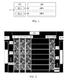
- FIG. 1 illustrates in block diagram form a simple display device embodiment taking an image input signal I and displays an image accordingly.
- the display device has a display panel DP with a matrix of pixels arranged for operation according to a FSC principle.
- a control circuit CC with separate data lines DL1, DL2 are connected to respective groups of pixels GP1, GP2.
- the control circuit CC is arranged to separately refresh the two groups of pixels GP1, GP2, and especially the control circuit CC may operate according to a scanning scheme where at least one pixels in both of the two groups of pixels GP1, GP2 are refreshed simultaneously.
- the total refresh time is reduced if is assumed that the charging time for each pixel is maintained, and thus frame rate capacity of the display device is double compared to prior art technique.
- the pixels may be divided.
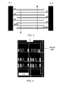
- FIG. 2 illustrates one concept for data line DL and gate line G_L, G_R configuration of a display device embodiment, e.g. a TFT based LCD display device arranged to operate according to an FSC principle.
- a display device embodiment e.g. a TFT based LCD display device arranged to operate according to an FSC principle.
- One gate line G_L is connected to odd horizontal lines of pixels L1, L3, L1079, while the other gate line G_R is connected to even horizontal lines of pixels L2, L4, L1080.
- Charging of even line pixels L2, L4, L1080 and odd line pixels L1, L3, L1079 is done simultaneously by the respective even and odd gates line drivers G_R, G_L. In this way full addressing of a display panel can be done in half of the normal time.
- the number of gate lines will remain the same, i.e. 1080 lines in case of a FHD display, however, split up in two groups for even and odd lines (2* 540 lines).
- each data path for each data line DL is in this case per definition 50% of conventional (each data line drives 540 pixels), the electrical resistance, given the same data line design, is equal, therefore the timing in the display for charging the TFT cell is halved. Thus, from an electrical point of view doubling the timing would also be possible.
- FIG. 3 illustrates one possible scanning scheme for the embodiment of FIG. 2 , namely scanning of odd lines pixels L1, L3, L1079 from top to bottom and simultaneously scanning of even lines pixels L2, L4, L1080 from bottom to top.
- Such scanning scheme is beneficial for reducing image flicker which could be visible in FSC systems, especially at lower refresh rates.
- FIG. 4 illustrates a timing diagram showing timing for the scanning scheme of FIG. 3 as well as the scanning timing for a conventional display device, indicated as "PRIOR ART".
- conventional scanning of all 1080 lines takes time T
- simultaneous scanning of two lines i.e. one even number horizontal line and one odd number horizontal line
- the total scanning of the 1080 lines is completed in half the time T, i.e. T/2.
- the charging time for each line is the same in both cases.
- FIG. 5 illustrates another possible scanning scheme for the embodiment of FIG. 2 , namely simultaneous scanning of a pair of neighbor horizontal lines, i.e. one pair being L1 and L2, the next pair being L3 and L4, and scanning is performed from top to bottom.
- This scanning scheme may be preferred since it preserves a more correct motion portrayal.
- FIG. 6 illustrates a timing diagram showing timing for the scanning scheme of FIG. 5 , again compared to scanning in a conventional display device, indicated as "PRIOR ART".
- scanning takes time T for all 1080 lines according to a conventional scanning scheme
- the same charging time will result in a total of half the scanning time T/2 since simultaneous scanning of two lines is performed.
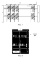
- FIG. 7 illustrates another concept for data line and gate line configuration, namely with separate data lines DL and one gate line G for an even and odd pair L1, L2 and L3, L4 horizontal screen line.
- a double number of datalines D1, D2 is used per vertical pixel line P1, thus making a total of 3840 data lines DL for a full HD display panel.
- FIG. 8 illustrates a timing diagram showing timing for the configuration of FIG. 7 compared to a conventional display device. Again, scanning of two lines simultaneously, here pairs of one even and one odd horizontal line allows completion of a scanning in time T/2 compared to time T for a conventional scanning scheme.
- FIG. 9 illustrates steps of a method embodiment, i.e. a method for refreshing pixels of a matrix of pixels arranged for displaying an image according to a color sequential scheme.
- a first data line connected to a first set of pixels is provided
- an in another step P_DL2 a second data line connected to a second set of pixels is provided.
- two steps R_SG1, R_SG2 are simultaneously performed: controlling the first data line to refresh a first group of pixels R_SG1, and controlling the second data line to refresh a second group of pixels R_SG2.
- the invention provides a display device arranged to display an image according to input data I according to a color sequential scheme.
- a display panel DP e.g. a TFT LCD panel, with a matrix of pixels GP1, GP2 controlled by a control circuit CC.
- the control circuit CC comprises separate first and second data lines DL1, DL2 connected to respective first and second sets of pixels GP1, GP2. Separate gate lines G_L, G_R may be provided to the two sets of pixels GP1, GP2.
- the control circuit CC controls the first and second data lines DL1, DL2 so as to separately refresh the two sets of pixels GP1, GP2.
- the two sets of pixels GP1, GP2 may be simultaneously refreshed, e.g. simultaneous refreshing of pairs of even number horizontal pixel lines L2, L4, L1080 and odd number horizontal pixel lines L1, L3, L1079. This can save 50% of scanning time, and thus increase frame rate capacity of the display device and further reduce color breakup and image flicker.
- a computer program may be stored/distributed on a suitable medium, such as an optical storage medium or a solid-state medium supplied together with or as part of other hardware, but may also be distributed in other forms, such as via the Internet or other wired or wireless telecommunication systems. Any reference signs in the claims should not be construed as limiting the scope.
Landscapes
- Engineering & Computer Science (AREA)
- Chemical & Material Sciences (AREA)
- Crystallography & Structural Chemistry (AREA)
- Physics & Mathematics (AREA)
- Computer Hardware Design (AREA)
- General Physics & Mathematics (AREA)
- Theoretical Computer Science (AREA)
- Liquid Crystal Display Device Control (AREA)
- Control Of Indicators Other Than Cathode Ray Tubes (AREA)
Abstract
A display device arranged to display an image according to input data (I) according to a color sequential scheme. A display panel (DP), e.g. a TFT LCD panel, with a matrix of pixels (GP1, GP2) controlled by a control circuit (CC). The control circuit (CC) comprises separate first and second data lines (DL1, DL2) connected to respective first and second sets of pixels (GP1, GP2). Separate gate lines (G_L, G_R) may be provided to the two sets of pixels (GP1, GP2). The control circuit (CC) controls the first and second data lines (DL1, DL2) so as to separately refresh the two sets of pixels (GP1, GP2). Especially, the two sets of pixels (GP1, GP2) may be simultaneously refreshed, e.g. simultaneous refreshing of pairs of even number horizontal pixel lines (L2, L4, L1080) and odd number horizontal pixel lines (L1, L3, L1079). This can save 50% of scanning time, and thus increase frame rate capacity of the display device and further reduce color breakup and image flicker.
Description
- The present invention relates to the field of display devices, more specifically, the invention relates to a Liquid Crystal Display (LCD) display and a method for driving an LCD display which allows a capability of handling high frame rates.
- A display device operating according to Field Sequential Color (FSC) technology only needs one pixel, "RGB" sub-pixels do not exist in FSC. This means that the number of source data lines in the FSC approach is reduced by 1/3 as compared to a conventional "RGB" TFT panel. However, with display devices operating according to FSC principle, an image quality problem is associated with the sequential display of the primary colors, often red, green, and blue. The problem is called "color breakup". This artefact, also referred to as the rainbow effect or color flash effect, is induced by the fact that in a sequential-color system the different color components of an image do not necessarily fall on the same location on the retina.
- Color breakup can be largely alleviated by increasing the refresh rate from 60 Hz to about 540 Hz or even more. However, with conventional Thin Film Transistor (TFT) LCD panels, required frame rates of at least 540 Hz are not yet feasible.
- This problem by FSC display devices is even more pronounced, in case the display device is arranged for displaying 3D images, where typically a double frame rate is required compared to normal 2D images, namely temporally adjacent frames intended for respective left eye and right eye of the viewer. To avoid serious left-right cross-talk, and thus a poor 3D effect, the refresh speed requirement of the display is thus even higher for 3D image reproduction.
- In line with the above description, a high frame rate capability is generally desirable for FSC display devices in order to produce high quality images. Thus, it would be advantageous to provide a FSC display device capable of providing a refresh rate higher than possible with known techniques.
- In a first aspect, the invention provides a display device arranged to receive input data and to display an image accordingly, the display device comprising
- a display panel comprising a matrix of pixels arranged for being driven according to a color sequential scheme, and
- a control circuit arranged to control the pixels according to the input data, wherein the control circuit comprises separate first and second data lines connected to respective first and second sets of pixels, and wherein the control circuit is arranged to control the first and second data lines so as to separately refresh the first and second sets of pixels.
- By providing a cell structure of the display device with separate data lines to two groups of pixels, it is possible to apply a scanning scheme which ensures a simultaneous scanning of the two pixel groups. Effectively, this means that the charging time is reduced by 50%, and thus a doubling of the refresh rate of the pixels can be obtained compared to prior art techniques. This enables an increased frame rate capability of the FSC display device, e.g. TFT based LCD devices, and allows improved image quality with reduced color breakup and image flicker effects.
- It is to be understood that the input data may be in any known form of image data, either conventional two dimensional (2D) image data or three dimensional (3D) image data. In case of 3D images based on presentation of sequential left-right images, the increased frame rate capability of the display device will result in presentation of 3D images with reduced left-right cross-talk, and thus improve the 3D image effect.
- In preferred embodiments, the control circuit is arranged to control the first and second data lines simultaneously so as to simultaneously refresh the first and second sets of pixels. With simultaneous refreshing of both groups of pixels, which is possible with the display device of the invention, the maximum increase in refresh speed is obtained. However, it is to be understood that a small delay between the refreshing of the first and second sets of pixels may be used, if desired.
- The separate first and second data lines of the display panel may be connected to respective even horizontal lines of pixels and odd horizontal lines of pixels. Thus, in this embodiment, two groups of pixels are formed: even horizontal lines (
i.e. line numbers 2, 4, 6...) in one group, and odd horizontal lines (i.e. line numbers 1, 3, 5...) in another group. This allows different possibilities of scanning schemes where these two groups of pixels are refreshed simultaneously. Especially, the display panel may comprise separate first and second gate line groups for the respective even horizontal lines of pixels and odd horizontal lines of pixels. Simultaneous scanning includes the use of different write timings / speeds for odd and even lines. A timing difference between odd and even line scanning may be used for black or grey line insertion which may be faster in nature than average video content scanning. Thus, although the general frame rate of the display will not change, the scanning scheme may be so that even lines are refreshed at a different speed (timing) than the odd lines. - The control circuit may be arranged to control scanning of horizontal lines of pixels according to one of the scanning schemes:
- 1) scanning odd horizontal lines of pixels from top to bottom and simultaneously scanning even horizontal lines of pixels from bottom to top, or
- 2) scanning even horizontal lines of pixels from top to bottom and simultaneously scanning odd horizontal lines of pixels from bottom to top.
- Alternatively, the control circuit may be arranged to control scanning of horizontal lines of pixels according to one of the scanning schemes:
- 1) scanning even horizontal lines of pixels and simultaneously scanning odd horizontal lines of pixels being adjacent to said even horizontal lines of pixels from top to bottom, or
- 2) scanning even horizontal lines of pixels and simultaneously scanning odd horizontal lines of pixels being adjacent to said even horizontal lines of pixels from bottom to top.
- According to another embodiment, the display panel comprises separate first and second gate line groups for the respective pairs of even horizontal lines of pixels and pairs of odd horizontal lines of pixels. Especially, the control circuit may be arranged to simultaneously scan pairs of even horizontal lines of pixels and pairs of odd horizontal lines of pixels from top to bottom or from bottom to top. Such scanning scheme with simultaneous refreshing of two neighbor horizontal lines may be preferred, in case correct motion portrayal is considered important. In the above embodiments, it is to be understood of course that equivalent embodiments can be formed with scanning schemes where "horizontal lines of pixels" is simply replaced by "vertical lines of pixels".
- The display device may be arranged to receive input data comprising 3D image information and to display an image with 3D image attributes accordingly. Especially, said 3D image attributes are provided by the display being arranged to display temporally separate images intended for viewing by respective left eye and right eye of a viewer. As mentioned, the high frame rate capability of the display device allows sequential 3D image presentation with reduces cross-talk and thus improved 3D effect.
- The display panel may comprise an LCD panel, and especially, the LCD panel may be implemented as a TFT panel.
- The control circuit may be arranged to refresh horizontal lines of pixels at a refresh rate of at least 400 Hz. However, it is to be understood that lower rates can be used, if desired, e.g. 100 Hz or lower, and alternatively, higher refresh rates may also be used, e.g. in the range 400-600 Hz, 600-1000 Hz or even higher, depending on the selected display panel technology.
- The display device may be a TV set, a computer monitor, or any handheld device, e.g. a mobile device with a display functionality, such as a tablet computer or a mobile phone. As mentioned, the invention can be used for display devices capable of presenting 2D as well as for 3D images with a high image quality. In embodiments where the invention is combined with blink and back light scanning, 3D cross-talk may be further reduced.
- It is to be understood, that the display device can be implemented in several ways. The display device may have the display panel and the control circuit placed within one common housing, however the control circuit may alternatively be placed in a separate unit and functionally connected to the display panel. The display panel may have different sizes and number of pixels. E.g. small display devices for mobile equipment may be 1" to 12", while monitors or TV sets may be such as 24" to 85", or even larger. Especially, the display panel may have a matrix of 1080 by 1920 pixels or an even higher resolution, thus enabling reproduction of full HD images. The invention is also applicable for display of RGBW, RGBY, or multi primary color pixels.
- In a second aspect, the invention provides a method for refreshing pixels of a matrix of pixels arranged for displaying an image according to a color sequential scheme, the method comprising
- providing separate first and second data lines connected to respective first and second sets of pixels, and
- controlling the first and second data lines so as to separately refresh the first and second sets of pixels.
- It is appreciated that the same advantages and embodiments of the first aspect apply as well for the second aspect. In general the first and second aspects may be combined and coupled in any way possible within the scope of the invention. These and other aspects, features and/or advantages of the invention will be apparent from and elucidated with reference to the embodiments described hereinafter.
- Embodiments of the invention will be described, by way of example only, with reference to the drawings, in which
-
Figure 1 shows a block diagram of a display device embodiment, -
Figure 2 illustrates data line and gate line configuration of a full HD embodiment, -
Figure 3 illustrates one possible scanning scheme for the embodiment ofFigure 2 , -
Figure 4 illustrates horizontal scanning timing for the scanning scheme ofFigure 3 compared to prior art, -
Figure 5 illustrates another scanning scheme for the embodiment ofFigure 2 , -
Figure 6 illustrates horizontal scanning timing for the scanning scheme ofFigure 5 compared to prior art, -
Figure 7 illustrates data line and gate line configuration of another full HD embodiment, -
Figure 8 , illustrates horizontal scanning timing for the scanning scheme ofFigure 7 compared to prior art, and -
Figure 9 illustrates a block diagram of a method embodiment. -
FIG. 1 illustrates in block diagram form a simple display device embodiment taking an image input signal I and displays an image accordingly. The display device has a display panel DP with a matrix of pixels arranged for operation according to a FSC principle. A control circuit CC with separate data lines DL1, DL2 are connected to respective groups of pixels GP1, GP2. For a full HD display panel e.g. two data lines can be provided for each vertical line of pixels. The control circuit CC is arranged to separately refresh the two groups of pixels GP1, GP2, and especially the control circuit CC may operate according to a scanning scheme where at least one pixels in both of the two groups of pixels GP1, GP2 are refreshed simultaneously. Hereby, the total refresh time is reduced if is assumed that the charging time for each pixel is maintained, and thus frame rate capacity of the display device is double compared to prior art technique. In principle, the pixels may be divided. -
FIG. 2 illustrates one concept for data line DL and gate line G_L, G_R configuration of a display device embodiment, e.g. a TFT based LCD display device arranged to operate according to an FSC principle. As seen, there are two separate data lines D1, D2 for each vertical line of pixels P1, and two gate lines G_L, G_R each connected to half of the horizontal lines of pixels. One gate line G_L is connected to odd horizontal lines of pixels L1, L3, L1079, while the other gate line G_R is connected to even horizontal lines of pixels L2, L4, L1080. Charging of even line pixels L2, L4, L1080 and odd line pixels L1, L3, L1079 is done simultaneously by the respective even and odd gates line drivers G_R, G_L. In this way full addressing of a display panel can be done in half of the normal time. - In case of a Full HD panel, the total number of data lines DL is 1920 x 2 = 3840 lines, a reduction of 33% as compared to the number of data lines in conventional "RGB" TFT panels. The number of gate lines will remain the same, i.e. 1080 lines in case of a FHD display, however, split up in two groups for even and odd lines (2* 540 lines). Writing an even L2, L4, L1080 and corresponding odd line L1, L3, L1079 simultaneously means that the display addressing is done in half the time enabling the double refresh rate of 480 Hz compared to a conventional 240 Hz case.
- The electrical capacity of each data path for each data line DL is in this case per definition 50% of conventional (each data line drives 540 pixels), the electrical resistance, given the same data line design, is equal, therefore the timing in the display for charging the TFT cell is halved. Thus, from an electrical point of view doubling the timing would also be possible.
- With the introduction of two separate gate drive groups, each for 540 lines, there is the possibility to deviate from conventional top-down scanning, and the configuration concept of
FIG. 2 allows several scanning schemes, since the two groups of pixels can be separately addressed. -
FIG. 3 illustrates one possible scanning scheme for the embodiment ofFIG. 2 , namely scanning of odd lines pixels L1, L3, L1079 from top to bottom and simultaneously scanning of even lines pixels L2, L4, L1080 from bottom to top. Such scanning scheme is beneficial for reducing image flicker which could be visible in FSC systems, especially at lower refresh rates. -
FIG. 4 illustrates a timing diagram showing timing for the scanning scheme ofFIG. 3 as well as the scanning timing for a conventional display device, indicated as "PRIOR ART". Where conventional scanning of all 1080 lines takes time T, simultaneous scanning of two lines, i.e. one even number horizontal line and one odd number horizontal line, the total scanning of the 1080 lines is completed in half the time T, i.e. T/2. The charging time for each line is the same in both cases. -
FIG. 5 illustrates another possible scanning scheme for the embodiment ofFIG. 2 , namely simultaneous scanning of a pair of neighbor horizontal lines, i.e. one pair being L1 and L2, the next pair being L3 and L4, and scanning is performed from top to bottom. This scanning scheme may be preferred since it preserves a more correct motion portrayal. -
FIG. 6 illustrates a timing diagram showing timing for the scanning scheme ofFIG. 5 , again compared to scanning in a conventional display device, indicated as "PRIOR ART". As before, where scanning takes time T for all 1080 lines according to a conventional scanning scheme, the same charging time will result in a total of half the scanning time T/2 since simultaneous scanning of two lines is performed. -
FIG. 7 illustrates another concept for data line and gate line configuration, namely with separate data lines DL and one gate line G for an even and odd pair L1, L2 and L3, L4 horizontal screen line. As inFIG. 2 , a double number of datalines D1, D2 is used per vertical pixel line P1, thus making a total of 3840 data lines DL for a full HD display panel. -
FIG. 8 illustrates a timing diagram showing timing for the configuration ofFIG. 7 compared to a conventional display device. Again, scanning of two lines simultaneously, here pairs of one even and one odd horizontal line allows completion of a scanning in time T/2 compared to time T for a conventional scanning scheme. -
FIG. 9 illustrates steps of a method embodiment, i.e. a method for refreshing pixels of a matrix of pixels arranged for displaying an image according to a color sequential scheme. In one step P_DL1, a first data line connected to a first set of pixels is provided, an in another step P_DL2, a second data line connected to a second set of pixels is provided. Then, two steps R_SG1, R_SG2 are simultaneously performed: controlling the first data line to refresh a first group of pixels R_SG1, and controlling the second data line to refresh a second group of pixels R_SG2. - To sum up, the invention provides a display device arranged to display an image according to input data I according to a color sequential scheme. A display panel DP, e.g. a TFT LCD panel, with a matrix of pixels GP1, GP2 controlled by a control circuit CC. The control circuit CC comprises separate first and second data lines DL1, DL2 connected to respective first and second sets of pixels GP1, GP2. Separate gate lines G_L, G_R may be provided to the two sets of pixels GP1, GP2. The control circuit CC controls the first and second data lines DL1, DL2 so as to separately refresh the two sets of pixels GP1, GP2. Especially, the two sets of pixels GP1, GP2 may be simultaneously refreshed, e.g. simultaneous refreshing of pairs of even number horizontal pixel lines L2, L4, L1080 and odd number horizontal pixel lines L1, L3, L1079. This can save 50% of scanning time, and thus increase frame rate capacity of the display device and further reduce color breakup and image flicker.
- While the invention has been illustrated and described in detail in the drawings and foregoing description, such illustration and description are to be considered illustrative or exemplary and not restrictive; the invention is not limited to the disclosed embodiments. Other variations to the disclosed embodiments can be understood and effected by those skilled in the art in practicing the claimed invention, from a study of the drawings, the disclosure, and the appended claims. In the claims, the word "comprising" does not exclude other elements or steps, and the indefinite article "a" or "an" does not exclude a plurality. A single processor or other unit may fulfill the functions of several items recited in the claims. The mere fact that certain measures are recited in mutually different dependent claims does not indicate that a combination of these measured cannot be used to advantage. A computer program may be stored/distributed on a suitable medium, such as an optical storage medium or a solid-state medium supplied together with or as part of other hardware, but may also be distributed in other forms, such as via the Internet or other wired or wireless telecommunication systems. Any reference signs in the claims should not be construed as limiting the scope.
Claims (15)
- A display device arranged to receive input (I) data and to display an image accordingly, the display device comprising- a display panel (DP) comprising a matrix of pixels (GP1, GP2) arranged for being driven according to a color sequential scheme, and- a control circuit (CC) arranged to control the pixels (GP1, GP2) according to the input data (I), wherein the control circuit (CC) comprises separate first and second data lines (DL1, DL2) connected to respective first and second sets of pixels (GP1, GP2), and wherein the control circuit (CC) is arranged to control the first and second data lines (DL1, DL2) so as to separately refresh the first and second sets of pixels (GP1, GP2).
- Display device according to claim 1, wherein the control circuit (CC) is arranged to control the first and second data lines (DL1, DL2) simultaneously so as to simultaneously refresh the first and second sets of pixels (GP1, GP2).
- Display device according to claim 1, wherein the separate first and second data lines (DL1, DL2) of the display panel are connected to respective even horizontal lines (L1, L4, L1080) of pixels and odd horizontal lines of pixels (L1, L3, L1079).
- Display device according to claim 3, wherein the display panel comprises separate first and second gate line groups (G_L, G_R) for the respective even horizontal lines of pixels (L2, L4, L1080) and odd horizontal lines of pixels (L1, L3, L1079).
- Display device according to claim 4, wherein the control circuit (CC) is arranged to control scanning of horizontal lines of pixels according to a scanning scheme being one of:- scanning odd horizontal lines of pixels (L1, L3, L1079) from top to bottom and simultaneously scanning even horizontal lines of pixels (L2, L4, L1080) from bottom to top, or- scanning even horizontal lines of pixels (L2, L4, L1080) from top to bottom and simultaneously scanning odd horizontal lines of pixels (L1, L3, L1079) from bottom to top.
- Display device according to claim 4, wherein the control circuit is arranged to control scanning of horizontal lines of pixels according to a scanning scheme being one of:- scanning even horizontal lines of pixels (L2, L4, L1080) and simultaneously scanning odd horizontal lines of pixels (L1, L3, L1079) being adjacent to said even horizontal lines of pixels (L2, L4, L1080) from top to bottom, or- scanning even horizontal lines of pixels (L2, L4, L1080) and simultaneously scanning odd horizontal lines of pixels (L1, L3, L1079) being adjacent to said even horizontal lines of pixels from bottom to top.
- Display device according to claim 3, wherein the display panel comprises separate first and second gate line groups (G_L, G_R) for the respective pairs of even horizontal lines of pixels (L2, L4, L1080) and pairs of odd horizontal lines of pixels (L1, L3, L1079).
- Display device according to claim 7, wherein the control circuit is arranged to simultaneously scan pairs of even horizontal lines of pixels (L2, L4, L1080) and pairs of odd horizontal lines of pixels (L1, L3, L1079) from top to bottom or from bottom to top.
- Display device according to claim 1, being arranged to receive input data (I) comprising three dimensional image information and to display an image with three dimensional image attributes accordingly.
- Display device according to claim 9, wherein said three dimensional image attributes are provided by the display being arranged to display temporally separate images intended for viewing by respective left eye and right eye of a viewer.
- Display device according to claim 1, wherein the display panel (DP) comprises a Liquid Crystal Display panel.
- Display device according to claim 3, wherein the Liquid Crystal Display panel is implemented as a Thin Film Transistor panel.
- Display device according to claim 1, wherein the control circuit is arranged to refresh horizontal lines of pixels at a refresh rate of at least 400 Hz.
- Display device according to claim 1, being one of: a TV set, a computer monitor, and a hand-held device.
- Method for refreshing pixels of a matrix of pixels arranged for displaying an image according to a color sequential scheme, the method comprising- providing separate first and second data lines connected to respective first and second sets of pixels, and- controlling the first and second data lines so as to separately refresh the first and second sets of pixels.
Priority Applications (1)
| Application Number | Priority Date | Filing Date | Title |
|---|---|---|---|
| EP11174606A EP2549468A1 (en) | 2011-07-20 | 2011-07-20 | Display device with high frame rate capability |
Applications Claiming Priority (1)
| Application Number | Priority Date | Filing Date | Title |
|---|---|---|---|
| EP11174606A EP2549468A1 (en) | 2011-07-20 | 2011-07-20 | Display device with high frame rate capability |
Publications (1)
| Publication Number | Publication Date |
|---|---|
| EP2549468A1 true EP2549468A1 (en) | 2013-01-23 |
Family
ID=44936628
Family Applications (1)
| Application Number | Title | Priority Date | Filing Date |
|---|---|---|---|
| EP11174606A Withdrawn EP2549468A1 (en) | 2011-07-20 | 2011-07-20 | Display device with high frame rate capability |
Country Status (1)
| Country | Link |
|---|---|
| EP (1) | EP2549468A1 (en) |
Cited By (1)
| Publication number | Priority date | Publication date | Assignee | Title |
|---|---|---|---|---|
| CN104282286A (en) * | 2014-10-30 | 2015-01-14 | 广东欧珀移动通信有限公司 | Method and system for adjusting display refresh rate of smart mobile terminal according to application scene |
Citations (5)
| Publication number | Priority date | Publication date | Assignee | Title |
|---|---|---|---|---|
| EP1780702A1 (en) * | 2005-10-26 | 2007-05-02 | Samsung Electronics Co., Ltd. | Liquid crystal display and method of driving the same |
| US20070120810A1 (en) * | 2005-11-28 | 2007-05-31 | Lg.Philips Lcd Co., Ltd. | Display device and method for driving the same |
| US20070279370A1 (en) * | 2006-06-02 | 2007-12-06 | Au Optronics Corporation | Field-sequential liquid crystal display and method for driving the same |
| US20080088566A1 (en) * | 2006-10-14 | 2008-04-17 | Au Optronics Corp. | Driving system and method for color sequential liquid crystal display (lcd) |
| US20100134523A1 (en) * | 2005-08-12 | 2010-06-03 | Thales | Sequential colour matrix display and addressing method |
-
2011
- 2011-07-20 EP EP11174606A patent/EP2549468A1/en not_active Withdrawn
Patent Citations (5)
| Publication number | Priority date | Publication date | Assignee | Title |
|---|---|---|---|---|
| US20100134523A1 (en) * | 2005-08-12 | 2010-06-03 | Thales | Sequential colour matrix display and addressing method |
| EP1780702A1 (en) * | 2005-10-26 | 2007-05-02 | Samsung Electronics Co., Ltd. | Liquid crystal display and method of driving the same |
| US20070120810A1 (en) * | 2005-11-28 | 2007-05-31 | Lg.Philips Lcd Co., Ltd. | Display device and method for driving the same |
| US20070279370A1 (en) * | 2006-06-02 | 2007-12-06 | Au Optronics Corporation | Field-sequential liquid crystal display and method for driving the same |
| US20080088566A1 (en) * | 2006-10-14 | 2008-04-17 | Au Optronics Corp. | Driving system and method for color sequential liquid crystal display (lcd) |
Cited By (1)
| Publication number | Priority date | Publication date | Assignee | Title |
|---|---|---|---|---|
| CN104282286A (en) * | 2014-10-30 | 2015-01-14 | 广东欧珀移动通信有限公司 | Method and system for adjusting display refresh rate of smart mobile terminal according to application scene |
Similar Documents
| Publication | Publication Date | Title |
|---|---|---|
| US10417954B2 (en) | Display panel and display device | |
| US8723194B2 (en) | Array substrate and pixel unit of display panel | |
| US8063876B2 (en) | Liquid crystal display device | |
| US11056057B2 (en) | Array substrate, display apparatus, and method of driving array substrate | |
| US10923052B2 (en) | Liquid crystal display device | |
| US8179356B2 (en) | Method for driving liquid crystal display with inserting gray image | |
| US20130135451A1 (en) | Stereoscopic Image Displaying Apparatus and Corresponding Stereoscopic Image Displaying Method | |
| US12512081B2 (en) | Display apparatus and control method thereof | |
| US12494184B2 (en) | Display driving method, display driving device, and display device | |
| US20130021385A1 (en) | Lcd device and black frame insertion method thereof | |
| TWI446327B (en) | Image processing method and related apparatus for a display device | |
| JP5728895B2 (en) | Electro-optical device and electronic apparatus | |
| US9470900B2 (en) | Display unit, display driving circuit, and display driving method | |
| KR20150076442A (en) | Liquid crystal display | |
| CN113707065B (en) | Display panel, display panel driving method and electronic device | |
| US8803763B2 (en) | Electro-optical device and electronic apparatus | |
| US20180174541A1 (en) | Display device and image control method for display device | |
| CN117423322B (en) | Driving method of display panel and display device | |
| CN220569384U (en) | Spliced display screen, display control equipment and display screen system | |
| KR102423615B1 (en) | Timing controller and display apparatus having the same | |
| CN117423323A (en) | Driving method and display device of display panel | |
| US20120176351A1 (en) | Dot inversion tft array and lcd panel | |
| US20120113319A1 (en) | Display device and display method | |
| CN104361867B (en) | Splice screen display device and its display drive method | |
| US10690980B2 (en) | Array substrate and driving method thereof and liquid crystal panel |
Legal Events
| Date | Code | Title | Description |
|---|---|---|---|
| PUAI | Public reference made under article 153(3) epc to a published international application that has entered the european phase |
Free format text: ORIGINAL CODE: 0009012 |
|
| AK | Designated contracting states |
Kind code of ref document: A1 Designated state(s): AL AT BE BG CH CY CZ DE DK EE ES FI FR GB GR HR HU IE IS IT LI LT LU LV MC MK MT NL NO PL PT RO RS SE SI SK SM TR |
|
| AX | Request for extension of the european patent |
Extension state: BA ME |
|
| RAP1 | Party data changed (applicant data changed or rights of an application transferred) |
Owner name: KONINKLIJKE PHILIPS N.V. |
|
| STAA | Information on the status of an ep patent application or granted ep patent |
Free format text: STATUS: THE APPLICATION IS DEEMED TO BE WITHDRAWN |
|
| 18D | Application deemed to be withdrawn |
Effective date: 20130724 |