EP2549281A1 - Microcontroller, control device and determination method - Google Patents
Microcontroller, control device and determination method Download PDFInfo
- Publication number
- EP2549281A1 EP2549281A1 EP12174189A EP12174189A EP2549281A1 EP 2549281 A1 EP2549281 A1 EP 2549281A1 EP 12174189 A EP12174189 A EP 12174189A EP 12174189 A EP12174189 A EP 12174189A EP 2549281 A1 EP2549281 A1 EP 2549281A1
- Authority
- EP
- European Patent Office
- Prior art keywords
- pwm signal
- unit
- pwm
- pulse width
- pulse
- Prior art date
- Legal status (The legal status is an assumption and is not a legal conclusion. Google has not performed a legal analysis and makes no representation as to the accuracy of the status listed.)
- Granted
Links
Images






Classifications
-
- G—PHYSICS
- G06—COMPUTING OR CALCULATING; COUNTING
- G06F—ELECTRIC DIGITAL DATA PROCESSING
- G06F11/00—Error detection; Error correction; Monitoring
- G06F11/07—Responding to the occurrence of a fault, e.g. fault tolerance
- G06F11/0703—Error or fault processing not based on redundancy, i.e. by taking additional measures to deal with the error or fault not making use of redundancy in operation, in hardware, or in data representation
- G06F11/0751—Error or fault detection not based on redundancy
- G06F11/0754—Error or fault detection not based on redundancy by exceeding limits
-
- G—PHYSICS
- G06—COMPUTING OR CALCULATING; COUNTING
- G06F—ELECTRIC DIGITAL DATA PROCESSING
- G06F11/00—Error detection; Error correction; Monitoring
- G06F11/07—Responding to the occurrence of a fault, e.g. fault tolerance
- G06F11/0703—Error or fault processing not based on redundancy, i.e. by taking additional measures to deal with the error or fault not making use of redundancy in operation, in hardware, or in data representation
- G06F11/0706—Error or fault processing not based on redundancy, i.e. by taking additional measures to deal with the error or fault not making use of redundancy in operation, in hardware, or in data representation the processing taking place on a specific hardware platform or in a specific software environment
- G06F11/0736—Error or fault processing not based on redundancy, i.e. by taking additional measures to deal with the error or fault not making use of redundancy in operation, in hardware, or in data representation the processing taking place on a specific hardware platform or in a specific software environment in functional embedded systems, i.e. in a data processing system designed as a combination of hardware and software dedicated to performing a certain function
- G06F11/0739—Error or fault processing not based on redundancy, i.e. by taking additional measures to deal with the error or fault not making use of redundancy in operation, in hardware, or in data representation the processing taking place on a specific hardware platform or in a specific software environment in functional embedded systems, i.e. in a data processing system designed as a combination of hardware and software dedicated to performing a certain function in a data processing system embedded in automotive or aircraft systems
-
- G—PHYSICS
- G06—COMPUTING OR CALCULATING; COUNTING
- G06F—ELECTRIC DIGITAL DATA PROCESSING
- G06F13/00—Interconnection of, or transfer of information or other signals between, memories, input/output devices or central processing units
-
- Y—GENERAL TAGGING OF NEW TECHNOLOGICAL DEVELOPMENTS; GENERAL TAGGING OF CROSS-SECTIONAL TECHNOLOGIES SPANNING OVER SEVERAL SECTIONS OF THE IPC; TECHNICAL SUBJECTS COVERED BY FORMER USPC CROSS-REFERENCE ART COLLECTIONS [XRACs] AND DIGESTS
- Y02—TECHNOLOGIES OR APPLICATIONS FOR MITIGATION OR ADAPTATION AGAINST CLIMATE CHANGE
- Y02D—CLIMATE CHANGE MITIGATION TECHNOLOGIES IN INFORMATION AND COMMUNICATION TECHNOLOGIES [ICT], I.E. INFORMATION AND COMMUNICATION TECHNOLOGIES AIMING AT THE REDUCTION OF THEIR OWN ENERGY USE
- Y02D10/00—Energy efficient computing, e.g. low power processors, power management or thermal management
Definitions
- the present invention relates to a microcontroller having a diagnostic function of a pulse width modulation (PWM) timer, a control device having the microcontroller built therein, and a determination method for determining whether the diagnostic function in the microcontroller is normal, and particularly to a technology effective if applied to a microcontroller having a PWM timer built therein, which needs to have higher reliability.
- PWM pulse width modulation
- a microcontroller has been incorporated into each of devices such as a household electric appliance, an AV device, a cellular phone, an automobile and an industrial machine or the like.
- the microcontroller is of a semiconductor integrated circuit which performs processing in accordance with a program stored in a memory to thereby perform control on the respective devices.
- Parts including the microcontrollers incorporated into these devices need reliability according to their use.
- the parts including the microcontrollers to have high reliability because there is a possibility that the breakdown of a control device can lead to accidents.
- an automobile microcontroller needs to have the function of bringing a safety device into action to detect the occurrence of a breakdown when it has occurred and prevent the automobile from being brought to a dangerous condition. Therefore, the microcontroller needs to not only detect failures in, for example, a sensor, an actuator and the like target for control by performing diagnosis on those but also detect a failure in the microcontroller itself.
- Patent Document 1 has disclosed a technology in which in a timer circuit, a process for a logical addition of a count value of a counter circuit in the timer circuit and an inverted value of an immediately preceding count value is performed, and a count operation is determined to be abnormal when its added value is "0 (zero)", after which the result of its determination is notified to the outside.
- the Patent Document 2 has disclosed a technology in which an automobile electronic control unit equipped with a microcontroller and an output driver circuit diagnoses earthing/powering and breaking of the output driver circuit, overcurrent of a power transistor and overtemperature of the power transistor.
- the Patent Document 3 has disclosed a technology in which a microcontroller provided with a plurality of processing systems each comprised of a CPU and a memory compares data processed by the CPUs of the respective processing systems to detect abnormalities of the processing systems.
- a PWM system is known as one of motor's drive control systems.
- the microcontroller gives a pulse signal having a period enough shorter than the number of revolutions of the motor and its pulse width is changed to thereby control supply energy.
- a central processing unit (CPU) installed in a microcontroller calculates a pulse period and a pulse width of a PWM pulse signal corresponding to the target value and sets the calculated pulse period and pulse width to a register lying within a PWM timer installed in the microcontroller.
- the PWM timer outputs a PWM pulse signal corresponding to the set values.
- the technology of the Patent Document 1 is applied to the automobile microcontroller with respect to this need, it is possible to detect an abnormality of a counter circuit in the PWM timer.
- the technology of the Patent Document 1 is however not capable of conducting inspections as to whether the pulse period and pulse width of the output PWM pulse signal being as set and the like and is insufficient as for failure inspection.
- the inventors of the present application have therefore studied about a method for diagnosing a failure in the PWM timer prior to the invention of the present application.
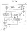
- FIG. 19 is a block diagram showing one example of a microcontroller having a diagnostic function of a PWM timer studied by the inventors of the present application prior to the invention.
- the PWM timer 81 has a signal generation unit 82 which generates a PWM signal corresponding to a pulse period and a pulse width set by a CPU 11, and a pulse detection unit 83 which detects the rising and falling edges of the generated PWM signal.
- the signal generation unit 82 counts a clock signal CLK input from a clock generator (CPG) 16 by a counter (CNTR) 823.
- a pulse generator (PG) 820 of the signal generator 82 generates and outputs a PWM signal 210, based on the count value of the counter 823 and the pulse period and pulse width set to each of the registers 821 and 822.
- the pulse detection unit 83 holds a count value at the time that the rising edge of the PWM signal 210 outputted from the signal generator 82 is detected, and a count value at the time that its falling edge is detected, in their corresponding registers 811 and 812.
- the pulse detection unit 83 When the pulse detection unit 83 detects the rising edge, it causes an interrupt generator (INT_CNT) 813 to generate an interrupt signal and notifies it to the CPU 11.
- INT_CNT interrupt generator
- the CPU 11 accesses the registers 811 and 812 in the pulse detection unit 83 and thereby acquires a count value related to the rising edge and a count value related to the falling edge. Then, the CPU 11 calculates a pulse period and a pulse width, based on the acquired count values and determines whether the results of calculation coincide with the pulse period and pulse width set to the signal generation unit 82.
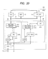
- FIG. 20 is a block diagram showing another example of a microcontroller having a diagnostic function of a PWM timer examined by the inventors of the present application prior to the invention.
- the microcontroller 201 shown in the same drawing is different from the above microcontroller 200 of FIG. 19 .
- a PWM timer 84 which generates a PWM signal, and a pulse detection unit 85 which detects the rising and falling edges of the generated PWM signal are configured as discrete circuit modules.
- the PWM timer 84 generates and outputs a PWM signal 211 by a method similar to the above signal generation unit 82.
- the pulse detection unit 85 holds a count value at the time that the rising edge of the PWM signal 211 is detected, and a count value at the time that the its falling edge is detected, in a register (REG_REDG) 811 and a register (REG_FEDG) 812 respectively.
- the pulse detection unit 85 When the rising edge is detected, the pulse detection unit 85 generates an interrupt signal and notifies it to a CPU 11. Then, the CPU 11 calculates a pulse period and a pulse width, based on the acquired count values and determines whether the results of calculation coincide with the pulse period and pulse width set to the signal generation unit 84.
- the microcontroller 200 shown in FIG. 19 and the microcontroller 201 shown in FIG. 20 as described above, it is possible to diagnose whether the pulse period and the pulse width of the PWM pulse signal generated by the PWM timer are as set.
- the CPUs respectively perform the process for determining whether the pulse widths and the pulse periods of the generated PWM pulse signals 210 and 211 coincide with the set values of the signal generation units 82 and 84 respectively, thereby increasing the processing loads of the CPUs.
- a preferred aim of the present invention is to provide a technology that enables a more detailed failure diagnosis on a PWM timer while suppressing an increase in processing load of a CPU provided in a microcontroller having the PWM timer built therein.
- a microcontroller (1 through 10) has a central processing unit (11), and a PWM signal generation unit (200, 21) which generates a PWM signal according to a generation condition set by the central processing unit. Further, the microcontroller has a diagnostic unit which detects a pulse period and a pulse width of the PWM signal, based on the PWM signal generated by the PWM signal generation unit and compares the detected pulse period and pulse width with the pulse period and pulse width of the PWM signal based on the generation condition to thereby perform a diagnosis of the PWM signal generation unit.
- the diagnostic unit may be configured as, for example, a diagnostic unit (201, 20, 30, 40) which inputs a PWM signal generated by the PWM signal generation unit therein and detects a pulse period and a pulse width, based on the input signal and which compares the detected pulse period and pulse width with a pulse period and a pulse width corresponding to the generation condition to thereby perform a diagnosis of the PWM signal generation unit.
- a diagnostic unit 201, 20, 30, 40
- the diagnostic unit rather than the central processing unit performs the process for the diagnosis, a failure decision of the PWM signal generation unit can be performed without increasing a processing load of the central processing unit. Comparing the detected pulse period and pulse width with the pulse period and pulse width corresponding to the generation condition enables a more detailed failure decision of the PWM signal generation unit.
- the diagnostic unit (40) corrects the input PWM signal to be a high level only for a first period (e.g., period corresponding to one clock cycle of a clock signal CLK) shorter than the pulse period for the set generation condition and detects a pulse period and a pulse width of the corrected PWM signal (190) to thereby perform the comparison.
- a first period e.g., period corresponding to one clock cycle of a clock signal CLK
- the PWM signal when the duty ratio 0% is set as the generation condition, the PWM signal is so corrected that the rising edge of the signal can be detected. Since it is thus possible to detect a pulse even in the case of the duty ratio 0%, a failure decision of the PWM signal generation unit can be performed even when the duty ratio 0% is set as the generation condition.
- the diagnostic unit (40) corrects the input PWM signal to be a low level only for a second period (e.g., period corresponding to one clock cycle of the clock signal CLK) shorter than the pulse period for the set generation condition and detects a pulse period and a pulse width of the corrected PWM signal (190) to thereby perform the comparison.
- a second period e.g., period corresponding to one clock cycle of the clock signal CLK
- the PWM signal when the duty ratio 100% is set as the generation condition, the PWM signal is so corrected that the falling edge of the signal can be detected. Since it is thus possible to detect a pulse even in the case of the duty ratio 100%, a failure decision of the PWM signal generation unit can be performed even when the duty ratio 100% is set as the generation condition.
- the diagnostic unit has a pulse correction unit (191) which corrects and outputs the input PWM signal according to the generation condition set to the PWM signal generation unit, a detection unit (171) which detects rising and falling edges of the signal outputted from the pulse correction unit, and a comparison unit (192) which calculates a pulse period and a pulse width of the signal outputted from the pulse correction unit, based on the detected edges and compares the calculated pulse period and pulse width with the pulse period and pulse width corresponding to the generation condition.
- a pulse correction unit (191) which corrects and outputs the input PWM signal according to the generation condition set to the PWM signal generation unit
- a detection unit (171) which detects rising and falling edges of the signal outputted from the pulse correction unit
- a comparison unit (192) which calculates a pulse period and a pulse width of the signal outputted from the pulse correction unit, based on the detected edges and compares the calculated pulse period and pulse width with the pulse period and pulse width corresponding to the generation condition.
- the pulse correction unit When the generation condition under which the pulse width of the PWM signal becomes zero is set to the PWM signal generation unit, the pulse correction unit generates a first signal (virtual rising edge signal) which is brought to a high level only for the first period with a timing (e.g., a timing of a clock cycle 11 of FIG. 10 ) at which a time corresponding to a pulse period has elapsed from a rising edge of the immediately preceding PWM signal and takes a logical ORing of the first signal and the input PWM signal to thereby generate the post-correction PWM signal.
- a timing e.g., a timing of a clock cycle 11 of FIG. 10
- the comparison unit determines that a PWM signal corresponding to the generation condition has been generated if the calculated pulse period and the pulse period corresponding to the generation condition coincide with each other, and the calculated pulse width and the pulse width corresponding to the first period coincide with each other, and determines that the PWM signal corresponding to the generation condition has not been generated if the calculated pulse period and the pulse period corresponding to the generation condition do not coincide with each other or the calculated pulse width and the pulse width corresponding to the first period do not coincide with each other.
- the PWM signal can easily be corrected, and a failure decision of the PWM signal generation unit is facilitated.
- the pulse correction unit when the generation condition under which the pulse width and the pulse period of the PWM signal coincide with each other, is set to the PWM signal generation unit, the pulse correction unit generates a second signal (virtual falling edge signal) brought to a high level only for the second period with a timing (e.g., a timing of a clock cycle 14 of FIG. 11 ) at which a predetermine period has elapsed from the time when the input PWM signal has risen, and takes a logical ANDing of an inverted signal of the second signal and the input PWM signal to thereby generate the post-correction PWM signal.
- a timing e.g., a timing of a clock cycle 14 of FIG. 11
- the comparison unit determines that a PWM signal corresponding to the generation condition has been generated if the calculated pulse period and the pulse period corresponding to the generation condition coincide with each other and the calculated pulse width and a pulse width obtained by making the pulse width corresponding to the generation condition short by the second period coincide with each other, and the comparison unit determines that the PWM signal corresponding to the generation condition has not been generated if the calculated pulse period and the pulse period corresponding to the generation condition do not coincide with each other or the calculated pulse width and the pulse width shortened by the second period do not coincide with each other.
- the PWM signal can easily be corrected, and a failure decision of the PWM signal generation unit is facilitated.
- the PWM signal generation unit has a first register (152, 153) for storing therein the generation condition including the pulse period and pulse width.
- the diagnostic unit further includes a second register (183, 184) for storing therein information including the generation condition stored in the first register. Further, the diagnostic unit (30, 40) performs the determination, based on the generation condition stored in the second register.
- the microcontroller according to the paragraph 6 is provided with the registers for storing the generation condition in the PWM signal generation unit and the diagnostic unit respectively, thereby making it possible to more improve the reliability of the diagnostic unit.
- the diagnostic unit (30, 40, 170) monitors writing of the generation condition into the first register by the central processing unit, acquires the generation condition to be written by the central processing unit and stores the same in the second register.
- the central processing unit (11), the PWM signal generation unit (21) and the diagnostic unit (30, 40, 170) are coupled to one another via an internal bus (13).
- the central processing unit outputs an address value indicative of the first register and data related to the generation condition onto the internal bus when the generation condition is written into the first register.
- the diagnostic unit monitors an address value outputted onto the internal bus, and when the outputted address value is found to be the address value indicative of the first register, the diagnostic unit acquires the data related to the generation condition outputted onto the internal bus and holds the same in the second register.
- the diagnostic unit writes the generation condition into the second register.
- the microcontroller further includes a first terminal (POUT) for outputting the PWM signal generated by the PWM signal generation unit to the outside, and a second terminal (PIN) for inputting a signal from outside.
- the diagnostic unit may be capable of selecting the PWM signal outputted to the first terminal and the PWM signal inputted via the second terminal as PWM signals target for the determination.
- the first terminal and the second terminal are electrically coupled to each other outside the microcontroller, so that abnormalities in the function of outputting the PWM signal from the first terminal and the function of inputting each signal from the second terminal can also be diagnosed.
- the PWM signal generation unit (200) and the diagnostic unit (201) are configured within a common circuit module (15).
- the PWM signal generation unit (21) and the diagnostic unit (20, 30, 40) are configured as circuit modules separated from each other.
- the PWM signal generation unit and the diagnostic unit are comprised of discrete semiconductor chips, so that independence between a target for diagnosis and a diagnostic subject can be secured. They can therefore be applied to a safety standard that requires higher reliability. Arranging circuit blocks for the PWM signal generation unit and the diagnostic unit in isolation even where the PWM signal generation unit and the diagnostic unit are configured within the same semiconductor chip makes it possible to more improve reliability.
- the microcontroller (5 through 9) further includes a first bus (13) operated in a first bus clock (high speed clock) and to which the central processing unit is coupled, a second bus (52) operated in a second bus clock (low speed clock) different from the first bus clock and to which the PWM signal generation unit and the diagnostic unit are coupled, and a bus control unit (51) for controlling communications between the first bus and the second bus.
- the second bus clock is lower than the first bus clock in frequency.
- the PWM signal generation unit or the like that no requires high-speed processing is operated in an operation clock lower in speed than an operation clock for the central processing unit, thereby making it possible to suppress power consumption.
- a microcontroller (7) is of a microcontroller in which in the paragraph 1, the PWM signal generation unit is comprised of a plurality of lower PWM signal generation parts configured so as to generate a plurality of PWM signals different from one another, and a first selection unit is further provided which inputs the PWM signals outputted from the PWM signal generation unit and selects and outputs any of the input PWM signals, and in which the diagnostic unit inputs the PWM signal outputted from the first selection unit therein, detects a pulse period and a pulse width of the input PWM signal, based on the PWM signal and compares the detected pulse period and pulse width with the pulse period and pulse width of the PWM signal based on the generation condition.
- the microcontroller (7) has, for example, a central processing unit (11), a plurality of lower PWM signal generation units (21_1 through 21_M) which generate PWM signals according to generation conditions for the PWM signals set by the central processing unit, and a first selection unit (55) which inputs the PWM signals outputted from the lower PWM signal generation units therein and selects and outputs any of the input PWM signals. Also the microcontroller has a diagnostic unit (20) which inputs the PWM signal outputted from the first selection unit therein and detects a pulse period and a pulse width, based on the input signal and which determines whether the detected pulse period and pulse width respectively coincide with the pulse period and pulse width corresponding to the generation condition.
- a diagnostic unit (20) which inputs the PWM signal outputted from the first selection unit therein and detects a pulse period and a pulse width, based on the input signal and which determines whether the detected pulse period and pulse width respectively coincide with the pulse period and pulse width corresponding to the generation condition.
- a more detailed failure decision of the PWM signal generation unit can be conducted without increasing the processing load of the central processing unit. According to this, even when a plurality of PWM signals are generated, diagnosis can selectively be conducted by one diagnostic unit so that there is no need to provide diagnostic units according to the number of the generated PWM signals, thus contributing to a reduction in the area of the microcontroller.
- the microcontroller further includes a plurality of first terminals (POUT_1 through POUT_M) for outputting a plurality of PWM signals generated by the PWM signal generation unit to the outside, and a second terminal (PIN_1 through PIN_N) for receiving each PWM signal input by the first selection unit from outside.
- the first selection unit selects any one of the PWM signals outputted to the first terminals and outputs the same as a first PWM signal, and selects any one of the PWM signals input via the second terminal and outputs the same as a second PWM signal.
- the diagnostic unit may be capable of selecting the first PWM signal and the second PWM signal as PWM signals target for the determination.
- the first and second terminals are electrically coupled to each other outside the microcontroller, so that abnormalities in the function of outputting the PWM signal from each first terminal and the function of inputting the signal from the second terminal can also be diagnosed.
- Another microcontroller (8) is of a microcontroller which in the paragraph 1, has a function which inputs each PWM signal outputted from the PWM signal generation unit therein and detects a pulse period and a pulse width of the input PWM signal, based on the PWM signal, and compares the detected pulse period and pulse width with the pulse period and pulse width of the PWM signal based on the generation condition, and which further includes other diagnostic units different from the diagnostic unit.
- the microcontroller (8) has a central processing unit (11) and a PWM signal generation unit (21) which generates each PWM signal according to a generation condition for each PWM signal set by the central processing unit.
- the microcontroller has a plurality of diagnostic units (20_1 through 20_N) each of which inputs the PWM signal outputted from the PWM signal generation unit therein and detects a pulse period and a pulse width based on the input signal, and determines whether the detected pulse period and pulse width respectively coincide with the pulse period and pulse width corresponding to the generation condition.
- a more detailed failure decision of the PWM signal generation unit can be conducted without increasing the processing load of the central processing unit. According to this as well, since one PWM signal can be diagnosed by a plurality of diagnostic units, the reliability of a diagnosis result is improved.
- the microcontroller has a first terminal (POUT) for outputting each PWM signal generated by the PWM signal generation unit to the outside, and a plurality of second terminals (PIN_1 through PIN_N) for inputting signals from outside.
- the microcontroller further includes a first selection unit (62) having in association with the diagnostic units, a plurality of selection circuits (622_1 through 622_N) which respectively input the PWM signals input from the second terminals therein, select any one of the input PWM signals and output the same to the one diagnostic unit.
- Each of the diagnostic units may be capable of selecting the PWM signal outputted to the first terminal and the signal selected by the corresponding selection circuit as PWM signals target for the determination.
- the first and second terminals are electrically coupled to each other outside the microcontroller, so that abnormalities in the function of outputting the PWM signal from the first terminal and the function of inputting the signal from each second terminal can also be diagnosed.
- a further microcontroller (9) is of a microcontroller in which in the paragraph 1, the PWM signal generation unit includes m lower PWM signal generation units configured so as to generate m (where m: integer greater than or equal to 2) PWM signals different from one another, and a first section unit is further provided which inputs the PWM signals outputted from the PWM signal generation unit and selects and outputs any of the input PWM signals, and in which the diagnostic unit includes n (where n: integer greater than or equal to 1) lower diagnostic units each of which inputs the PWM signal outputted from the first selection unit therein and detects a pulse period and a pulse width of the input PWM signal, based on the PWM signal and each of which compares the detected pulse period and pulse width with the pulse period and pulse width of the PWM signal based on the generation condition.
- the microcontroller (9) has a central processing unit (11), m (where m: integer more than or equal to 1) lower PWM signal generation units (21_1 through 21_M) which generate PWM signals according to generation conditions for the PWM signals set by the central processing unit, and a first selection unit (65) which inputs a plurality of PWM signals (164_1 through 164_M and 165_1 through 165_N) outputted from the lower PWM signal generation units and selects and outputs any of the input PWM signals.
- m where m: integer more than or equal to 1
- lower PWM signal generation units 21_1 through 21_M
- a first selection unit (65) which inputs a plurality of PWM signals (164_1 through 164_M and 165_1 through 165_N) outputted from the lower PWM signal generation units and selects and outputs any of the input PWM signals.
- the microcontroller also has n (where n: integer greater than or equal to 1) lower diagnostic units (20_1 through 20_N) which respectively input the PWM signal outputted from the first selection unit therein and detect a pulse period and a pulse width, based on the input signal, and which respectively determine whether the detected pulse period and pulse width coincide with the pulse period and pulse width corresponding to the generation condition.
- the microcontroller further includes m first terminals (POUT_1 through POUT_M) for respectively outputting the generated m PWM signals to the outside, and a plurality of second terminals (PIN_1 through PIN_N) for respectively receiving the PWM signals input to the first selection unit from outside.
- the first selection unit has, in association with the diagnostic units, n selection circuits (651_1 through 651_N and 652_1 through 652_N) each of which selects any one of the m PWM signals outputted to the first terminals and outputs the same to the one diagnostic unit as a first PWM signal, and selects any one of the PWM signals input via the second terminals and outputs the same thereto as a second PWM signal.
- Each of the diagnostic units may be capable of selecting the PWM signal outputted to the first terminal and the signal selected by the corresponding selection circuit as PWM signals target for the determination.
- the first and second terminals are electrically coupled to each other outside the microcontroller, so that abnormalities in the function of outputting the PWM signal from each first terminal and the function of inputting the signal from each second terminal can also be diagnosed.
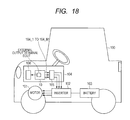
- a control device (104) is of a control device for controlling a motor.
- the control device includes a microcontroller (10) which generates each PWM signal for driving the motor and outputs an error signal from an external terminal (OUT) where the generated PWM signal is abnormal, a driver (105) for driving the motor (101), based on the generated PWM signal, and a safety device (106) which performs a process for preventing an abnormal operation of the motor in response to the error signal.
- the microcontroller has a central processing unit (11), a PWM signal generation unit (200, 21) which generates each PWM signal according to a generation condition set by the central processing unit, and a diagnostic unit (201, 20, 30, 40) which inputs the generated PWM signal therein and detects a pulse period and a pulse width thereof, based on the input PWM signal and which determines whether the detected pulse period and pulse width coincide with a pulse period and a pulse width corresponding to the generation condition. Further, the microcontroller outputs the error signal to the external terminal according to the result of determination.
- a failure decision of the PWM signal generation unit can be conducted without increasing the processing load of the central processing unit in the microcontroller. Comparing the detected pulse period and pulse width with the pulse period and pulse width corresponding to generation condition respectively enables a more detailed failure decision, thereby making it possible to more improve the safety of motor control.
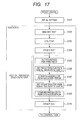
- a determination method is a determination method for determining whether a diagnostic unit of a microcomputer (1 through 9) having a PWM signal generation unit (200, 21) which generates each PWM signal according to a set generation condition, and the diagnostic unit (201, 20, 30, 40) which determines whether the PWM signal generated by the PWM signal generation unit is of a signal having a pulse period and a pulse width corresponding to a condition set thereto, is normal.
- the determination method includes a first step (S105 through S107) for setting a condition (first generation condition) equivalent to the generation condition (first generation condition) set to the PWM signal generation unit to the diagnostic unit, determining that the diagnostic unit is normal when the diagnostic unit determines that the generated PWM signal coincides with a PWM signal corresponding to the equivalent condition, and determining that the diagnostic unit is abnormal when the two are determined not to coincide with each other.
- the determination method has a second step (S108, S109) for setting a condition (second generation condition) different from the generation condition (first generation condition) set to the PWM signal generation unit to the diagnostic unit, determining that the diagnostic unit is abnormal when the generated PWM signal coincides with a PWM signal corresponding to the different condition, and determining that the diagnostic unit is normal when the two are determined not to coincide with each other.
- the diagnosis is conducted by the two of the first step for setting the condition equivalent to the generation condition set to the PWM signal generation unit and the second step for setting the condition different from the generation condition set to the PWM signal generation unit, the accuracy of diagnosis with respect to the diagnostic unit can be enhanced. It is thus possible to improve not only the reliability of the PWM signal generation unit but also the reliability of the diagnostic unit.
- FIG. 1 is a block diagram showing one example of a microcontroller equipped with a PWM timer function and its diagnostic function.
- the microcontroller (MCU) 1 shown in the same drawing is comprised of, for example. a CPU 11, a memory (MRY) 12, an internal bus 13, an interrupt controller (INT_CNT) 14, a PWM timer 15 and a clock generator (CPG) 16, and other unillustrated peripheral circuit modules.
- the CPU 11 is a processor which executes a command related to a program stored in the memory 12 or the like and performs processing such as an arithmetic operation, a data transfer, etc.
- the memory 12 includes a storage area for storing a program executed by the CPU 11 and data calculated by the corresponding program processing.
- the interrupt controller 14 receives interrupt requests from the peripheral circuit modules such as the PWM timer 15, etc.
- the clock generator 16 inputs an external clock signal EX_CLK generated by a crystal oscillator therein through an external terminal for example, generates a clock signal CLK high in precision, based on the input external clock signal EX_CLK, and supplies it to each circuit module in the microcontroller 1.
- the PWM timer 15 is equipped with a signal generating function unit 200 which generates a PWM signal, and a diagnostic function unit 201 which performs a diagnosis of the PWM signal.
- a signal generating function will first be explained.
- the PWM timer 15 has, as the signal generating function unit 200, e.g., a control register (REG_CNT) 151, a pulse period register (REG_PRD) 152, a pulse width register (REG_PW) 153, a pulse width buffer 154, a pulse generator (PG) 156 and a counter (CNTR) 157.
- the pulse generator 156 When the CPU 11 sets a condition for generating the PWM signal to each of the registers 151 through 153 via the internal bus 13, for example, the pulse generator 156 generates a PWM signal 164 based on a count value C_VAL of a clock signal CLK counted by the counter 157.
- the control register 151 is set with, by the CPU 11, e.g., information (hereinafter also referred to as pulse output control information) indicative of whether the pulse generator 156 performs the output of a PWM signal, selection information (hereinafter also called pulse selection information) for designating or specifying a PWM signal target for diagnosis to be described later, information (hereinafter also called interrupt generation control information) indicative of whether an interrupt is generated where the result of diagnosis to be described later is an error, and information (hereinafter also called comparison process control information) indicative of whether a comparison process should be performed by a comparator 161 to be described later.
- pulse output control information information indicative of whether the pulse generator 156 performs the output of a PWM signal
- selection information hereinafter also called pulse selection information
- interrupt generation control information information indicative of whether an interrupt is generated where the result of diagnosis to be described later is an error
- comparison process control information indicative of whether a comparison process should be performed by a comparator 161 to be described later.
- Th pulse period register 152 is set with, by the CPU 11, e.g., information indicative of a pulse period of a PWM signal to be generated.
- the pulse width register 153 is set with, by the CPU 11, e.g., information indicative of a pulse width of a PWM signal to be generated.
- the values set to the pulse period register 152 and the pulse width register 153 are values to be compared with the count value counted by the counter 157.
- the value set to the pulse period register 152 is assumed to specify the pulse period of a PWM signal being outputted at that time.
- the value set to the pulse width register 153 is assumed to be written into the pulse width buffer 154 at a timing provided to output a PWM signal to be next output.
- the value written into the pulse width buffer 154 is assumed to specify the pulse width of a PWM signal being in output at that time.
- the pulse width buffer 154 is a buffer for adjusting the timing provided to output the PWM signal having the pulse width set to the pulse width register 153.
- the value of the pulse width register 153 is set thereto. The details of the pulse width buffer 154 will be described later.
- the values of the control register 151, the pulse period register 152 and the pulse width register 153 are respectively outputted to the pulse generator 156, the comparator 161 and the interrupt generator 163.
- the counter 157 counts a clock CLK.
- the counter value C_VAL thereof is used to determine the pulse period and pulse width of the PWM signal.
- the pulse generator 156 monitors the count value C_VAL of the counter 157.
- the pulse generator 156 changes the level of the PWM signal 164 to a High level with the rise timing of the next clock signal CLK and outputs a write signal to the pulse width buffer 154 to cause the pulse width buffer 154 to write the value of the pulse width register 153.
- the pulse generator 156 further outputs a reset signal to the counter 157 to set the count value C_VAL to an initial value "1".
- the pulse generator 156 changes the level of the PWM signal 164 to a Low level with the next rise timing of the clock signal CLK.
- the value settable as the pulse width ranges from zero to the value of the pulse period.
- the PWM signal 164 becomes a signal (duty ratio 0%) of a low level during the whole one period.
- the PWM signal becomes a signal (duty ratio 100%) of a high level during the whole one period.
- FIG. 2 is a timing chart showing one example illustrative of operation timings of the PWM timer 15.
- the same drawing shows where the pulse periods of two PWM signals different in pulse width are assumed to be values extremely short in pulse period, but not limited to these.
- the frequency of the clock signal CLK is 20MHz during an actual operation
- the PWM signal 164 is a pulse period of 20kHz or so and becomes 1000 cycles.
- the clock signal CLK is assigned numbers indicative of clock cycles in the same drawing.
- signals outputted to the internal bus 13 include a ready signal RDY, a command signal CMD, an address signal A and write data WD.
- the ready signal RDY indicates whether a bus command CMD is valid or invalid. When it is valid, the ready signal RDY becomes "1 (High)”. When it is invalid, the ready signal RDY becomes "0 (Low)".
- the bus command CMD indicates the type of access of the CPU 11. "W” indicates a write command, and "N” indicates a command (NOP: Non Operation) indicating that nothing is done.
- An address A includes addresses for registers and a memory targeted for access by the CPU 11.
- the write data WD is data to be written into a register or the like specified by the address A.
- the CPU 11 In a clock cycle 1 as shown in the same drawing, the CPU 11 outputs a write command W and an address A1 to the internal bus 13.
- the address A1 is an address for the pulse period register 152.
- the CPU 11 In the next clock cycle 2, the CPU 11 outputs write data D1. Then, when the write data D1 is written into the pulse period register 152 in a clock cycle 3, the counter 157 starts counting. In the clock cycle 3, the CPU 11 outputs a write command W and an address A2 to the internal bus 13.
- the address A2 is an address for the pulse width register 153.
- the CPU 11 In the next clock cycle 4, the CPU 11 outputs write data D2.
- the pulse generator 156 determines the pulse width based on not the pulse width buffer 154, but instead the pulse width register 153, the value of the pulse width register 153 is reflected as the pulse width of a PWM signal being output where the PWM signal is written into the pulse width register 153 with a timing prior to its fall timing.
- the value of the pulse width register 153 can not be reflected as the pulse width of the PWM signal being output at that time. That is, when the timing provided to perform writing into the pulse width register 153 by the CPU 11 and the fall timing of the pulse occur one after another, the value set to the pulse width register 153 may not be reflected on the PWM signal.
- the value of the pulse width register 153 is written into the pulse width buffer 154 in the timing (e.g., the clock cycles 7 and 11 in FIG. 2 ) at which the next pulse period is started, and the pulse width of the PWM signal is determined based on the value set to the pulse width buffer 154.
- the PWM timer 15 By repeatedly performing the above processing, the PWM timer 15 generates a PWM signal in accordance with the generation condition of the PWM signal set by the CPU 11.
- the diagnostic function of the PWM timer 15 has, as diagnostic function unit 201, e.g., a flip-flop circuit (FF) 158, a pulse selector (SLCTR) 159, an edge detector (DTCT_EDG) 160, a comparator (CMP) 161, a status register (REG_ST) 162, and an interrupt generator (INT) 163.
- diagnostic function unit 201 e.g., a flip-flop circuit (FF) 158, a pulse selector (SLCTR) 159, an edge detector (DTCT_EDG) 160, a comparator (CMP) 161, a status register (REG_ST) 162, and an interrupt generator (INT) 163.
- FF flip-flop circuit
- SLCTR pulse selector
- DTCT_EDG edge detector
- CMP comparator
- REG_ST status register
- INT interrupt generator
- the pulse selector 159 selects a PWM signal target for diagnosis from input PWM signals and outputs it to the edge detector 160. For example, the pulse selector 159 inputs therein a PWM signal 164 outputted from the pulse generator 156 and an external PWM signal 165 inputted from an external input terminal PIN and selects and outputs either one of the PWM signals. Whether either of the PWM signals should be selected is determined according to the pulse selection information set to the control register 151.
- the edge detector 160 detects the rising and falling edges of the PWM signal 166 selected by the pulse selector 159 and outputs an edge detection signal.
- the flip-flop circuit 158 outputs a count value (hereinafter also called a count delay value) CD_VAL obtained by delaying the count value C_VAL by one cycle of the clock signal CLK.
- the comparator 161 takes in a count delay value CD_VAL of the flip-flop circuit 158 at the time that the rising edge has been detected, and a count delay value CD_VAL of the flip-flop circuit 158 at the time that the falling edge has been detected. Then, the comparator 161 compares the value of the flip-flop circuit 158 at the detection of the rising edge and the value of the pulse period register 152 with each other and determines whether they coincide with each other. Further, the comparator 162 compares the value of the flip-flop circuit 158 at the detection of the falling edge, and the value set to the pulse width register 153 with each other and determines whether they coincide with each other. The results of determination are outputted to the status register 162.
- the status register 162 has a failure detection bit indicative of whether the comparator 161 has detected an incoincidence. For example, when the comparator 161 has detected an incoincidence in pulse period or pulse width, it holds a value indicative of an error and continues to hold that value even subsequently.
- the interrupt generator 163 monitors the status register 162. When information indicative of an error is set to the status register 162, the interrupt generator 163 issues an interrupt request to the interrupt controller 14. Whether an interrupt should be generated where the comparator 161 has detected the incoincidence in pulse period or pulse width, is determined according to the interrupt generation control information set to the control register 151.
- the comparator 161 performs a comparison process C2 for comparing the count delay value CD_VAL and the value of the pulse period register 152. That is, as mentioned above, the rise timing of the pulse and the timing provided to start counting by the counter 157 are matched with each other and a count delay value CD_VAL obtained by delaying the count value C_VAL is generated, so that the value of the count delay value CD_VAL at the timing of the rising edge can be read as the value of the pulse period of the PWM signal 164. Accordingly, the count delay value CD_VAL read at the corresponding timing and the value of the pulse period register 152 are compared with each other to thereby make it possible to determine whether the PWM signal having the pulse period as set has been generated.
- a process (C3) for comparison of a pulse width is performed in a clock cycle 14, and a process (C4) for comparison of a pulse period is carried out in a clock cycle 15.
- the pulse width and the pulse period of the PWM signal are detected to thereby enable a diagnosis as to whether the PWM signal is generated as defined in the generation condition set by the CPU 11. It is thus possible to make a detailed failure diagnosis of the PWM timer 15. Since the process for the above diagnosis is realized not by the CPU 11 but the edge detector 160, the comparator 161 and the like, it is possible to determine the failure of the PWM timer 15 without increasing the processing load of the CPU 11.
- an external output terminal POUT and an external input terminal PIN are electrically coupled to each other outside the microcontroller 1 to input the PWM signal 164 generated by the pulse generator 156 via the external input terminal PIN, so that it is also possible to diagnose the input PWM signal. According to it, it is also possible to diagnose whether the function of outputting the PWM signal 164 from the external output terminal POUT and the function of inputting the PWM signal from the external input terminal PIN are normal.
- the microcontroller 1 whether an interrupt should be generated when an error in the PWM signal is detected, can be determined depending on the interrupt generation control information of the control register 151, thus increasing the degree of freedom of system design. Setting an interrupt request so as not to be generated, for example, enables such a system that when the error in the PWM signal is detected, the CPU 11 performs a process corresponding to the error detection after the completion of a process being in execution without interrupting the process being in execution. In this case, for example, the CPU 11 may be designed so as to access the status register 162 on a regular basis and monitor its value.
- the microcontroller 1 can share in common the circuit between the functional unit for generating the PWM signal and the functional unit for diagnosing the PWM signal. Since the functional unit for diagnosing the PWM signal can be utilized as a reference for diagnosing the values of the pulse period register 152, the pulse width register 153 and the pulse width buffer 154, for example, it is not necessary to separately provide a register or the like for setting the generation condition.
- the count delay value CD_VAL is generated using the count value C_VAL of the counter 157, which is used as a reference for generating the PWM signal, there is no need to provide a counter separately for the purpose of a diagnostic function.
- the microcontroller 1 it is possible to suppress an increase in chip area with the addition of the diagnostic function to the existing PWM timer 15. Particularly when a PWM timer 15 is newly designed, this can be said to be an effective means.
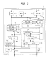
- FIG. 3 is a block diagram showing one example of a microcontroller equipped with a PWM timer function and its diagnostic function, according to a second embodiment.
- the PWM timer 15 is configured so as include the functional unit for generating the PWM signal and the functional unit for diagnosing the PWM signal.
- a functional unit for diagnosing a PWM signal is configured as another circuit module independent of a PWM timer.
- the microcontroller 2 has a PWM signal diagnostic unit 20 in addition to the PWM timer 21.
- the same reference numerals are respectively attached to the same components as those in the microcontroller 1 of FIG. 1 in the same drawing, and their detailed description will be omitted.
- the PWM signal diagnostic unit 20 includes a pulse selector (SLCTR) 159, a counter (CNTR) 172, an edge detector (DTCT_EDG) 171, a rising edge register (REG_REDG) 173, a comparator (CMP) 176, a status register (REG_ST) 162, a control register (REG_CNT) 174 and an interrupt generator (INT) 163.
- SLCTR pulse selector
- CNTR counter
- DTCT_EDG edge detector
- REG_REDG rising edge register
- CMP comparator
- REG_ST control register
- INT interrupt generator
- the pulse selection information, the interrupt generation control information and the comparison process control information are set to the control register 174 by a CPU 11 through an internal bus 13.
- the pulse output control information is set to its corresponding control register 151 provided within the PWM timer 21.
- the counter 172 counts a clock signal CLK independently of a counter 157 provided in the PWM timer 21.
- the counter 172 may be a counter that performs initialization every period of a PWM signal 164 as with the counter 157.
- the counter 172 is however illustrated by way of example as a free running counter that does not perform initialization.
- the pulse selector 159 selects a PWM signal corresponding to the pulse selection information set to the control register 174 and supplies the same to the edge detector 171.
- the edge detector 171 detects the rising and falling edges of the PWM signal 166 selected by the pulse selector 159. When the edge detector 171 detects the falling edge of the selected PWM signal, it instructs the rising edge register 173 to write a count value CF_VAL of the counter 172 and instructs the comparator 176 to execute a comparison process. Likewise, even in the case where the rising edge of the selected PWM signal is detected, the edge detector 171 instructs the comparator 176 to execute a comparison process.
- the rising edge register 173 holds therein a count value CF_VAL at that time.
- the comparator 176 When the comparator 176 receives therein the instruction for execution of the comparison process outputted when the edge detector 171 has detected the rising edge, the comparator 176 obtains a count value CF_VAL of the counter 172 at that time and the value of the rising edge register 173 and calculates the pulse period of the PWM signal 166, based on the thus-obtained value. Further, the comparator 176 compares the value of the calculated pulse period and the value of the pulse period register 152 in the PWM timer 21 and outputs the result of comparison to the status register 162. The pulse period is calculated by, for example, subtracting the value of the rising edge register 173 from the count value CF_VAL acquired on the rising edge.
- the comparator 176 When the comparator 176 receives therein the instruction for execution of the comparison process at the detection of the falling edge by the edge detector 171, the comparator 176 acquires a count value CF_VAL of the counter 172 at that time, and the value of the rising edge register 173 and calculates the pulse width of a PWM signal 166, based on the thus-acquired value. Further, the comparator 176 compares the value of the calculated pulse width and the value of a pulse width buffer 154 in the PWM timer 21 and outputs the result of comparison to the status register 162. The pulse width is calculated by, for example, subtracting the value of the rising edge register 173 from the count value CF_VAL acquired on the falling edge. Incidentally, whether the comparator 176 performs the comparison process is determined in accordance with the comparison process control information set to the control register 174.
- the status register 162 holds a value indicative of an error and continues to hold that value even after that.
- the interrupt generator 163 monitors the status register 162 and information indicative of an error is set to the status register 162, the interrupt generator 163 issues an interrupt request 17 to an interrupt controller 14. Whether or not an interrupt is generated where the inconsistency in pulse period or width is detected, is determined according to the interrupt generation control information set to the control register 174.
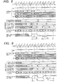
- FIG. 4 is a timing chart showing one example illustrative of operating timings of the PWM timer 21 and the PWM signal diagnostic unit 20.
- the setting of carrying out a pulse output is made to the control register 151, and the pulse selector 159 selects and outputs a PWM signal 164.
- the clock signal CLK is assigned numbers indicative of clock cycles in the same drawing.
- each timing provided to generate the PWM signal 164 is similar to FIG. 2 .
- the edge detector 171 detects the rising edge of the PWM signal 164 in a clock cycle 7
- the comparator 176 calculates a pulse width thereof and performs a comparison process C1 for comparing the result of calculation and the value of the pulse width buffer 154.
- the comparator 176 calculates a pulse period thereof and performs a comparison process C2 for comparing the result of comparison and the value of the pulse period register 152.
- a process for comparison with respect to a pulse width is performed in a cock cycle 14, and a process for comparison with respect to a pulse period is carried out in a clock cycle 15.
- the microcontroller 2 According to the microcontroller 2 according to the second embodiment as described above, a more detailed failure decision of the PWM timer 21 can be carried out without increasing the processing load of the CPU 11.
- the microcontroller 2 has an advantage that since it is equipped with the PWM signal diagnostic unit 20 as the circuit module independent of the PWM timer 21, the PWM timer part needs less modifications even where the PWM timer 21 is designed using the existing design resources.
- Arranging circuit blocks for the PWM timer 21 and the PWM signal diagnostic unit 20 in isolation where the PWM timer 21 and the PWM signal diagnostic unit 20 are configured within the same semiconductor chip enables a further improvement in reliability. If the PWM timer 21 and the PWM signal diagnostic unit 20 are comprised of discrete semiconductor chips, independence between a target for diagnosis and a diagnostic subject can be secured. They can therefore be applied to a safety standard that requires higher reliability.
- FIG. 5 is a block diagram showing one example of a microcontroller equipped with a PWM timer function and its diagnostic function, according to a third embodiment.
- the same reference numerals are respectively attached to the same components as those in the microcontrollers 1 and 2, and their detailed description will be omitted.
- the microcontroller 3 shown in the same drawing is provided inside a PWM signal diagnostic unit 30, with registers each of which stores information about the condition of generation of a PWM signal used in the diagnosis of the PWM signal.
- the PWM signal diagnostic unit 30 has a pulse selector (SLCTR) 159, a counter (CNTR) 172, an edge detector (DTCT_EDG) 171, a rising edge register (REG_REDG) 173, a comparator (CMP) 186, a register control circuit 170, a status register (REG_ST) 162, a control register (REG_CNT) 174, a snoop register (REG_SNP_A) 181, a snoop register (REG_SNP_B) 182, a pulse period register (REG_PRD) 183, a pulse width register (REG_PW) 184, a pulse width buffer 185 and an interrupt generator (INT) 163.
- SLCTR pulse selector
- CNTR counter
- DTCT_EDG edge detector
- REG_REDG rising edge register
- CMP comparator
- snoop control information indicative of whether a snoop function based on the register control circuit 170 to be described later should be made valid is set to the control register 174 in addition to the pulse selection information, the interrupt generation control information and the comparison process control information.
- the pulse period register 183 is set with information indicative of a pulse period of a PWM signal set to a pulse period register 152 of a PWM timer 21.
- the pulse width register 184 is set with information indicative of a pulse width of the PWM signal set to a pulse width register 153 of the PWM timer 21.
- the settings of the pulse period register 183 and the pulse width register 184 are achieved by the snoop function of the register control circuit 170, for example.
- the register control circuit 170 monitors each address value outputted onto an internal bus 13 and writes write data outputted onto the internal bus 13 into the register in the PWM signal diagnostic unit 30, corresponding to the outputted address value. When, for example, an address value of the control register 174 is outputted onto the internal bus 13, the register control circuit 170 acquires the write data outputted onto the internal bus 13 and writes the same into the control register 174.
- the register control circuit 170 is provided with the snoop function. Described concretely, when address values corresponding to values stored in the snoop registers 181 and 182 are outputted onto the internal bus 13, the register control circuit 170 acquires write data outputted to the internal bus 13 and writes the acquired write data into predetermined registers associated with the snoop registers 181 and 182. Address values for registers or the like target for snooping are set to the snoop registers 181 and 182.
- the register control circuit 170 acquires write data corresponding to the address value of the pulse period register 152 when the address value is outputted onto the internal bus 13, and writes the acquired write data into the pulse period register 183.
- the register control circuit 170 acquires write data corresponding to the address value of the pulse width register 153 when the address value is outputted onto the internal bus 13, and writes the acquired write data into the pulse period register 184. According to this, since the CPU 11 needs not to set the generation condition to the pulse period register 183 and the pulse width register 184 for the purpose of diagnosis of the PWM signal, it is possible to suppress an increase in the processing load of the CPU 11 related to the diagnosis of the PWM signal.
- each of the pulse period register 183 and the pulse width register 184 is assigned a unique address, and the CPU 11 can also specify the address and obtain access thereto.
- the comparator 186 When the comparator 186 receives an instruction for execution of a comparison process outputted when the edge detector 171 has detected a rising edge, the comparator 186 acquires a count value CF_VAL of the counter 172 at that time and the value of the rising edge register 173 and calculates the pulse period of the PWM signal 166, based on the acquired values. Further, the comparator 186 compares the value of the calculated pulse period and the value of the pulse period register 183 and outputs the result of comparison to the status register 162. The calculation of the pulse period is carried out by, for example, subtracting the value of the rising edge register 173 from the count value CF_VAL obtained on the rising edge.
- the comparator 186 When the comparator 186 receives an instruction for execution of a comparison process outputted when the edge detector 171 has detected a falling edge, the comparator 186 acquires a count value CF_VAL of the counter 172 at that time and the value of the rising edge register 173 and calculates the pulse width of the PWM signal 166, based on the acquired values. Further, the comparator 186 compares the value of the calculated pulse width and the value of the pulse width buffer 185 and outputs the result of comparison to the status register 162. The calculation of the pulse width is carried out by, for example, subtracting the value of the rising edge register 173 from the count value CF_VAL obtained on the falling edge.
- FIG. 6 is a timing chart showing one example illustrative of operation timings of the PWM timer 21 and the PWM signal diagnostic unit 30.
- the setting of pulse outputting has been made to the control register 151 and the pulse selector 159 selects and outputs a PWM signal 164 in the same drawing as with FIGS. 2 and 4 .
- an address (A1) of the pulse period register 152 in the PWM timer 21 is written into the snoop register 181 of the PWM signal diagnostic unit 30, and an address (A2) of the pulse width register 153 in the PWM timer 21 is written into the snoop register 182.
- a clock signal CLK is assigned numbers indicative of clock cycles in the same drawing.
- each timing provided to generate the PWM signal 164 is similar to FIGS. 2 and 4 .
- the same condition as the generation condition set to the PWM timer 21 is set to the PWM signal diagnostic unit 30.
- the edge detector 171 detects the rising edge of the PWM signal 164 in a clock cycle 7
- the value of the pulse width register 183 is written into the pulse width buffer 185 in the next clock cycle 8.
- the comparator 186 calculates a pulse width and performs a comparison process C1 for comparing the result of comparison and the value of the pulse width buffer 185.
- the comparator 186 calculates a pulse period thereof and performs a comparison process C2 for comparing the result of comparison and the value of the pulse period register 183.
- the microcontroller 3 can have each expected value of the PWM signal independent of the pulse period register 152, pulse width register 153 and pulse width buffer 154 provided in the PWM timer 21 due to the provision of the pulse period register 183, pulse width register 184 and pulse width buffer 185 within the PWM signal diagnostic unit 30. It is possible to improve reliability more than the PWM signal diagnostic unit 20 according to the second embodiment.
- the PWM signal diagnostic unit 30 is provided with the snoop function according to the microcontroller 3. There is therefore no need to perform the process for writing to the registers 183 through 185 by the CPU 11, and an increase in the processing load of the CPU 11 can be suppressed.
- FIG. 7 is a block diagram showing one example of a microcontroller equipped with a PWM timer function and its diagnostic function, according to a fourth embodiment.
- the same reference numerals are respectively attached to the same components as those in the microcontrollers 1 through 3, and their detailed description will be omitted.
- the microcontroller 4 shown in the same drawing is capable of diagnosing a PWM signal even when duty ratios 0% and 100% are set as conditions for the generation of a PWM signal.
- FIG. 8 illustrates by way of example where the PWM signal of the duty ratio 0% is generated.
- FIG. 9 illustrates by way of example where the PWM signal of the duty ratio 100% is generated.
- the PWM signal diagnostic unit 40 is equipped with a pulse correction circuit (P_REV) 191 in addition to the components of the PWM signal diagnostic unit 30 according to the third embodiment.
- P_REV pulse correction circuit
- the PWM signal diagnostic unit 40 corrects the PWM signal by means of the pulse correction circuit 191 and performs a diagnostic process based on the post-correction PWM signal 190.
- the pulse correction circuit 191 monitors a pulse period register 183, a pulse width register 184 and a pulse width buffer 185.
- the pulse correction circuit 191 corrects a PWM signal 166 outputted from a pulse selector 159 according to conditions for the generation of a PWM signal set to each of these and thereby outputs the same to an edge detector 171. For example, when the pulse width set to the pulse width register 184 is zero, and the pulse width set to the pulse width buffer 185 and the pulse period set to the pulse period register 183 coincide with each other, the pulse correction circuit 191 outputs the corrected signal of the input PWM signal 166 as a PWM signal 190. When a condition other than the two generation conditions is set, the pulse correction circuit 191 outputs the input PWM signal 166 as the PWM signal 190 without its correction.
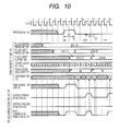
- FIG. 10 is a timing chart showing one example illustrative of operation timings of the PWM signal diagnostic unit 40 where a PWM signal having a duty ratio 0% is diagnosed.
- the setting of pulse outputting has been made to the control register 151 and the pulse selector 159 selects and outputs a PWM signal 164 in the same drawing as with FIG. 6 .
- an address (A1) of the pulse period register 152 in the PWM timer 21 is written into its corresponding snoop register 181 of the PWM signal diagnostic unit 40
- an address (A2) of the pulse width register 153 in the PWM timer 21 is written into its corresponding snoop register 182.
- the pulse correction circuit 191 does not correct the input PWM signal 164. That is, the pulse correction circuit 191 outputs the PWM signal 164 as a PWM signal 190 during a period from a clock cycle 7 to a clock cycle 10.
- the pulse correction circuit 191 generates a virtual rising edge signal in a timing (clock cycle 11) at which one period has elapsed from the rising edge (clock cycle 7) of a PWM signal having an immediately preceding period. Described specifically, when a value obtained by adding the value of the rising edge register 173 and the value of the pulse period register 183 coincides with a count value CF_VAL, the pulse correction circuit 191 generates a virtual falling edge signal.
- the same drawing shows an example in which the pulse width of the virtual rising edge signal is assumed to be a pulse width corresponding to one clock cycle of the clock signal CLK.
- the pulse width of the virtual rising edge signal is set to the pulse width corresponding to one clock cycle of the clock signal CLK although, if the virtual rising edge signal is of a signal that rises with the above timing, its pulse width is not limited in particular, it becomes easy to generate the virtual rising edge signal, thereby making it possible to simplify the configuration of the pulse correction circuit 191.
- the pulse correction circuit 191 outputs a signal of logical ORing of the virtual rising edge signal generated by the above method and the input PWM signal 164 as a PWM signal 190. That is, a PWM signal 190 is generated which is brought to a high level by one clock cycle with the timing of the clock cycle 11 during one period from the clock cycles 11 to 14. A similar correction is performed even at the timing of a subsequent clock cycle 15. Thus, even when the PWM signal 164 of the duty ratio 0% is generated, edge detection can be carried out using the post-correction PWM signal 190.
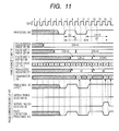
- FIG. 11 is a timing chart showing one example illustrative of operation timings of the PWM signal diagnostic unit 40 where a PWM signal having a duty ratio 100% is diagnosed.
- the setting of pulse outputting is assumed to be made to the control register 151, and the pulse selector 159 is assumed to select and output a PWM signal 164.
- the address (A1) of the pulse period register 152 in the PWM timer 21 is written into its corresponding snoop register 181 of the PWM signal diagnostic unit 40
- the address (A2) of the pulse width register 153 in the PWM timer 21 is written into its corresponding snoop register 182.
- the operation timings up to the clock cycle 8 are similar to FIG. 10 as shown in the same drawing.
- the pulse correction circuit 191 generates a virtual falling edge signal in a timing (clock cycle 10) at which a period shorter than a pulse period has elapsed from the timing (clock cycle 11) of the rising edge of the next PWM signal 164.
- a value obtained by subtracting only "1 (corresponding to one clock cycle)" from a value obtained by adding the value of the rising edge register 173 and the value of the pulse period register 183, and a count value CF_VAL coincide with each other, the pulse correction circuit 191 generates the virtual falling edge signal.
- the value "1 (corresponding to one clock cycle) to be subtracted is a value that defines the pulse width of the virtual falling edge signal. If the virtual falling edge signal is generated before one period of the PWM signal 164 of the duty ratio 100% elapses although the value to be subtracted is defined as "1 (corresponding to one clock cycle) in the above-described example, the value thereof is not limited.
- the pulse width is set as the pulse width corresponding to one clock cycle of the clock signal CLK although the pulse width of the virtual falling edge signal is not limited in particular, it becomes easy to generate a virtual falling edge signal, thereby making it possible to simplify the configuration of the pulse correction circuit 191.
- the pulse correction circuit 191 generates an inverted signal of the virtual falling edge signal generated by the above method and outputs as a PWM signal 190, a signal obtained by ANDing the inverted signal and the input PWM signal 164. That is, a PWM signal 190 brought to a low level by one clock cycle is generated with the timing of the clock cycle 14. Thus, even when the PWM signal 164 of the duty ratio 100% is generated, edge detection can be performed using the post-correction PWM signal 190.
- the edge detector 171 When the edge detector 171 detects the rising edge of the PWM signal 190 output from the pulse correction circuit 191 as with the third embodiment, the edge detector 171 instructs the rising edge register 173 to write the count value CF_VAL of the counter 172 and instructs the comparator 186 to execute a comparison process. Likewise, even where the rising edge of the PWM signal 190 is detected, the edge detector 171 instructs the comparator 186 to execute a comparison process.
- the comparator 192 monitors the pulse period register 183, the pulse width register 184 and the pulse width buffer 1985. When conditions other than the two generation conditions (duty ratio 0% and duty ratio 100%) are set, the comparator 192 executes a comparison process by a method similar to the third embodiment and outputs the result of comparison to the status register 162.
- the content of processing of the comparator 192 is as follows where the generation condition (the value of the pulse width register 184 is zero) for the duty ratio 0% is set.
- the comparator 192 calculates a pulse period and performs a comparison process for comparing the result of calculation and the value of the pulse period register 152.
- the edge detector 171 detects the falling edge of the PWM signal 190
- the comparator 192 calculates a pulse width and performs a comparison process for comparing the result of calculation and the value of the pulse period register 152. In a clock cycle 12 in the case of FIG.
- the content of processing of the comparator 192 where the generation condition (the value of the pulse width register 183 is zero) for the duty ratio 100% is set is as follows:
- the comparator 192 calculates a pulse period and performs a comparison process for comparing the result of calculation and the value of the pulse period register 152.
- the comparator 192 calculates a pulse width and performs a comparison process for comparing the result of calculation and the value of the pulse period register 152.
- a comparison process is carried out in consideration of the fact that the PWM signal 164 of the duty ratio 100% is corrected to a PWM signal 190 brought to a pulse width corresponding to three clock cycles by the correction of the PWM signal by the pulse correction circuit 190. It is thus possible to determine whether the PWM signal 164 having the duty ratio 100% is generated according to the generation condition.
- a more detailed failure decision of the PWM timer 21 can be carried out without increasing the processing load of the CPU 11 as with the first through third embodiments.
- An increase in the processing load of the CPU 11 can be suppressed by the snoop function while securing independence of a target for diagnosis of the PWM signal diagnostic unit 40.
- the diagnosis of the output of the PWM timer 21 is enabled even under the condition free of the occurrence of a pulse edge by the provision of the pulse correction circuit 191, thereby making it possible to improve a fault detection rate and achieve a further improvement in reliability.
- FIG. 12 is a block diagram showing one example of a microcontroller equipped with a PWM timer function and its diagnostic function, according to a fifth embodiment.
- the same reference numerals are respectively attached to the same components as those in the microcontrollers 1 through 4, and their detailed description will be omitted.
- the microcontroller 5 shown in the same drawing has two buses of an internal bus 13 and a system bus 52.
- a PWM timer is coupled to the system bus 52.
- the PWM timer is of the PWM timer 15 equipped with the diagnostic function according to the first embodiment.
- the system bus 52 operates in a low speed bus clock (low speed clock).
- An interrupt controller 14, the PWM timer 15 and a bus bridge (BUS_BRG) 51 are coupled to the system bus 52.
- the internal bus 13 operates in a bus clock (high speed clock) faster than the system bus 52.
- a CPU 11, a memory 12 and the bus bridge 51 are coupled to the internal bus 13.
- the bus bridge 51 controls communications between a circuit coupled to the internal bus 13 and a circuit coupled to the system bus 52.
- Such a hierarchical bus configuration is effective particularly where the CPU 11 is operated at high speed. For example, when the CPU 11 accesses the peripheral circuit coupled to the system bus 52, the pipeline of the CPU 11 stops until its access is completed, thus causing wastage of processing. The larger the ratio in clock frequency between the internal bus 13 and the system bus 52 in particular, the more the number of needless cycles increases. Therefore, when the CPU 11 performs the process related to the diagnosis of the PWM timer as in the studied related art example described above, the wastage of processing increases, thus inhibiting the high-speed operation of the CPU 11.
- the processing related to the diagnosis of the PWM timer by the CPU 11 becomes unnecessary because the PWM timer 15 itself is provided with the diagnostic function, thus enabling the high-speed operation of the CPU 11.
- the hierarchical bus configuration allows the CPU 11 and the memory 12 to operate in a high speed clock and allows the peripheral circuits such as the PWM timer 15, the interrupt controller 14 and the like unnecessary to operate at high speed to operate in a slow clock, thereby making it possible to suppress power consumption of the entire microcontroller.
- FIG. 13 is a block diagram showing one example of a microcontroller equipped with a PWM timer function and its diagnostic function, according to a sixth embodiment.
- the same reference numerals are respectively attached to the same components as those in the microcontrollers 1 through 5, and their detailed description will be omitted.
- the microcontroller 6 shown in the same drawing has two buses of an internal bus 13 and a system bus 52 as with the microcontroller 5 according to the fifth embodiment.
- a PWM timer and a PWM signal diagnostic unit are coupled to the system bus 52.
- the PWM timer 21 in the second embodiment can be applied as the PWM timer shown in the same drawing.
- Any of the PWM signal diagnostic units 20, 30 and 40 in the second through fourth embodiments can be applied as the PWM signal diagnostic unit.
- FIG. 13 typically shows as one example where the PWM signal diagnostic unit 20 is applied.
- the fifth embodiment it is possible to cause a CPU 11 to reduce a processing load related to the diagnosis of the PWM timer 21 and to suppress power consumption of the entire microcontroller.
- the setting of expected values for the pulse period and pulse width to the PWM signal diagnostic units 30 and 40 realized by the snoop function prevents the processing load related to the diagnosis of the CPU 11 from increasing.
- FIG. 14 is a block diagram showing one example of a microcontroller equipped with a PWM timer function and its diagnostic function, according to a seventh embodiment.
- the same reference numerals are respectively attached to the same components as those in the microcontrollers 1 through 6, and their detailed description will be omitted.
- the microcontroller 7 shown in the same drawing has two buses of an internal bus 13 and a system bus 52 as with the microcontroller 6 according to the sixth embodiment.
- M (where M: integer greater than or equal to 2)
- PWM timers 21_1 through 21_M each used as a PWM signal generation unit for generating PWM signals, and a single PWM signal diagnostic unit are coupled to the system bus 52.
- the PWM timers 21_1 through 21_M shown in the same drawing the PWM timer 21 in the second embodiment can be applied.
- the PWM signal diagnostic unit any of the PWM signal diagnostic units 20, 30 and 40 used in the second through fourth embodiments can be applied.
- FIG. 14 typically shows as one example where the PWM signal diagnostic unit 20 is applied.
- PWM signals 164_1 through 164_M respectively generated by the M PWM timers 21_1 through 21_M are outputted through M external output terminals POUT_1 through POUT_M.
- the microcontroller 7 has N (where N: integer greater than or equal to 1) external input terminals PIN_1 through PIN_N, which enable the input of PWM signals (external PWM signals) from the outside of the microcontroller.
- the generated PWM signals 164_1 through 164_M and the external PWM signals 165_1 through 165_N are inputted to a selection unit 55.
- the selection unit 55 has, for example, a first selection circuit 551 and a second selection circuit 552.
- the first selection circuit 551 inputs the respective PWM signals 164_1 through 164_M therein, selects any of the input signals, based on a selection signal 56 and outputs the selected signal to the PWM signal diagnostic unit 20 as a PWM signal 164.
- the second selection circuit 552 inputs the respective external PWM signals 165_1 through 165_N therein, selects any of the input signals, based on a selection signal 57 and outputs the selected signal to the PWM signal diagnostic unit 20 as an external PWM signal 165.
- the selection signals 56 and 57 are signals for giving instructions as to which PWM signal should be selected and outputted, and are outputted from a diagnosis pulse selection instruction unit 54.
- the diagnosis pulse selection instruction unit 54 has a control register 541 reprogrammable or writable through the system bus 52.
- a signal generator 542 generates and outputs the selection signals 56 and 57 in accordance with the value set to the control register 541.
- a more detailed fault decision of the PWM timer can be done without increasing the processing load of the central processing unit. Since diagnosis can selectively be conducted by the single PWM signal diagnostic unit even where a plurality of PWM signals are generated, there is no need to provide diagnostic units depending on the number of generated PWM signals, thus contributing to a reduction in the area of the microcontroller.
- the external output terminals POUT_1 through POUT_M and the external input terminals PIN_1 through PIN_N are electrically coupled to one another outside the microcontroller so that the PWM signals 164_1 through 164_M generated by the PWM timers 21_1 through 21_M are respectively inputted via the external input terminals PIN_1 through PIN_N, thus making it possible to select and diagnose each input signal. According to this, it is also possible to diagnose whether the function of outputting the PWM signals from the external output terminals POUT_1 through POUT_M and the function of inputting the PWM signals from the external input terminals PIN_1 through PIN_N are normal.
- FIG. 15 is a block diagram showing one example of a microcontroller equipped with a PWM timer function and its diagnostic function, according to an eighth embodiment.
- the same reference numerals are respectively attached to the same components as those in the microcontrollers 1 through 7, and their detailed description will be omitted.
- the microcontroller 8 shown in the same drawing has two buses of an internal bus 13 and a system bus 52 as with the microcontroller 6.
- a single PWM timer 21 and N (where N: integer greater than or equal to 2) PWM signal diagnostic units are coupled to the system bus 52.
- N integer greater than or equal to 2
- PWM signal diagnostic unit any of the PWM signal diagnostic units 20, 30 and 40 in the second through fourth embodiments can be applied.
- FIG. 15 typically shows as one example where the PWM signal diagnostic unit 20 is applied.
- a PWM signal 164 generated by the PWM timer 21 is inputted to the PWM signal diagnostic units 20_1 through 20_N respectively and outputted to the outside of the microcontroller 8 via an external output terminal POUT.
- the microcontroller 8 has N external input terminals PIN_1 through PIN_N, which enable the input of PWM signals (external PWM signals) from the outside of the microcontroller.
- the external PWM signals 165_1 through 165_N are inputted to a selection unit 62.
- the selection unit 62 has, for example, N third selection circuits 622_1 through 622_N.
- the third selection circuits 622_1 through 622_N are provided in association with one another every 20_1 through 20_N of PWM signal diagnostic units.
- the PWM signal diagnostic units 20_1 through 20_N respectively input the external PWM signals 165_1 through 165_N therein and select any of the input signals, based on corresponding selection signals 61_1 through 61_N. Further, the PWM signal diagnostic units 20_1 through 20_N output the selected signal to their corresponding PWM signal diagnostic units 20_1 through 20_N as the external PWM signal 165.
- the selection signals 61_1 through 61_N are signals for giving instructions as to which external PWM signals 165_1 through 165_N should be selected and outputted, and are outputted from a diagnostic pulse selection circuit 60.
- the diagnostic pulse selection circuit 60 has a control register 601 reprogrammable or writable through the system bus 52.
- a signal generator 602 generates and outputs the selection signals 61_1 through 61_N in accordance with the value set to the control register 601.
- a more detailed fault decision of the PWM timer can be done without increasing the processing load of the central processing unit. Since one PWM signal can be diagnosed by a plurality of diagnostic units, the reliability of the result of diagnosis can be enhanced.
- the external output terminal POUT and the external input terminals PIN_1 through PIN_N are electrically coupled to one another outside the microcontroller so that the PWM signal 164 generated by the PWM timer 21 is inputted via the external input terminals PIN_1 through PIN_N, thus making it possible to select and diagnose the input signal. According to this, it is also possible to diagnose whether the function of outputting the PWM signal from the external output terminal POUT and the function of inputting the PWM signal from the external input terminals PIN_1 through PIN_N are normal.
- FIG. 16 is a block diagram showing one example of a microcontroller equipped with a PWM timer function and its diagnostic function, according to a ninth embodiment.
- the same reference numerals are respectively attached to the same components as those in the microcontrollers 1 through 8, and their detailed description will be omitted.
- the microcontroller 9 shown in the same drawing has two buses of an internal bus 13 and a system bus 52 as with the microcontroller 6.
- M PWM timers 21 used as PWM signal generation units for generating PWM signals, and N PWM signal diagnostic units used as diagnostic units for diagnosing the PWM timer function are respectively coupled to the system bus 52.
- N PWM signal diagnostic units used as diagnostic units for diagnosing the PWM timer function are respectively coupled to the system bus 52.
- any of the PWM signal diagnostic units 20, 30 and 40 used in the second through fourth embodiments is applicable.
- FIG. 16 typically shows as one example where the PWM signal diagnostic unit 20 is applied.
- PWM signals 164_1 through 164_M respectively generated by the M PWM timers 21_1 through 21_M are respectively outputted through M external output terminals POUT_1 through POUT_M.
- the microcontroller 9 has N (where N: integer greater than or equal to 1) external input terminals PIN_1 through PIN_N, which enable the input of PWM signals (external PWM signals) 165_1 through 165_N from the outside of the microcontroller.
- the generated PWM signals 164_1 through 164_M and the external PWM signals 165_1 through 165_N are inputted to a selection unit 65.
- the selection unit 65 has, for example, fourth selection circuits 651_1 through 652_N and fifth selection circuits 652_1 through 652_N.
- the fourth selection circuits 651_1 through 651_N and the fifth selection circuits 652_1 through 652_N are provided in association with one another every 20_1 through 20_N of the PWM signal diagnostic units.
- the fourth selection circuit 651_1 through 651_N respectively input the PWM signals 164_1 through 164_M therein and select any of the input signals, based on their corresponding selection signals 63_1 through 63_N.
- the fourth selection circuits 651_1 through 651_N outputs the selected signal to their corresponding PWM signal diagnostic units 20_1 through 20_N as a PWM signal 164.
- the fifth selection circuits 652_1 through 652_N respectively input the external PWM signals 165_1 through 165_N therein, select any of the input signals, based on their corresponding selection signals 64_1 through 64_N, and output the selected signal to their corresponding PWM signal diagnostic units 20_1 through 20_N as an external PWM signal 165.
- the selection signals 63_1 through 63_N are signals for giving instructions as to which PWM signals 164_1 through 164_N should be selected and outputted.
- the selection signals 64_1 through 64_N are signals for giving instructions as to which PWM signals 165_1 through 165_N should be selected and outputted.
- the selection signals 63_1 through 63_N and the selection signals 64_1 through 64_N are outputted from a diagnostic pulse selection instruction unit 66.
- the diagnostic pulse selection instruction circuit 66 has a control register 661 reprogrammable or writable through the system bus 52.
- a signal generator 662 generates and outputs the selection signals 63_1 through 63_N and the selection signals 64_1 through 64_N in accordance with the value set to the control register 661.
- a more detailed fault decision of the PWM timer can be done without increasing the processing load of the central processing unit. Since the combination of a target for diagnosis and a diagnostic subject can freely be determined according to the respective numbers of the PWM timers 21_1 through 21_M and the PWM signal diagnostic units 20_1 through 210-N, the degrees of freedom of system design and a diagnostic method increase.
- the external output terminals POUT_1 through POUT_M and the external input terminals PIN_1 through PIN_N are electrically coupled to one another outside the microcontroller so that the PWM signals 164_1 through 164_M generated by the PWM timers 21 are respectively inputted via the external input terminals PIN_1 through PIN_N, thus making it possible to select and diagnose each input signal. According to this, it is also possible to diagnose whether the function of outputting the PWM signals from the external output terminals POUT_1 through POUT_M and the function of inputting the PWM signals from the external input terminals PIN_1 through PIN_N are normal.
- FIG. 17 is a flowchart showing one example of a diagnostic method of a diagnostic function for a PWM signal.
- a PWM signal diagnostic unit target for diagnosis by the present diagnostic method corresponds to each of the PWM signal diagnostic units 30 and 40 shown in the second through ninth embodiments.
- a diagnostic process for determining whether the PWM signal diagnostic unit is normal is included in, for example, a test process for confirming the operation of each of the various functional units in the microcontrollers 2 through 9 and is carried out before transition to the normal operation after a power-on reset, for example.
- the test process includes, e.g., a test on a memory 12, a test on a CPU 11 and a test on other functional units in addition to the test on the PWM timer.
- a test on the PWM signal diagnostic unit 30 is started.
- the CPU 11 first sets a generation condition (hereinafter also called a first generation condition) for generating, for example, a PWM signal having a first pulse period and a first pulse width to the registers 151 through 153 of the PWM timer 21 (S105).
- the values of the set first pulse period and pulse width are not limited in particular.
- the CPU 11 accesses the PWM signal diagnostic unit 30 and thereby sets the first generation condition to the pulse period register 183 and the pulse width register 184 (S106).
- the CPU 11 causes the PWM signal diagnostic unit 30 to execute a diagnostic process and confirms the result of its diagnosis (S107).
- the CPU 11 determines that the PWM signal diagnostic unit is abnormal. If not so, then the CPU 11 determines that the PWM signal diagnostic unit is normal.
- the CPU 11 accesses the PWM signal diagnostic unit 30 again and thereby sets a generation condition (hereinafter also called a second generation condition) for generating, for example, a PWM signal having a second pulse period and a second pulse width to the pulse period register 183 and the pulse width register 184 (S108).
- the second generation condition may be a generation condition different from the first generation condition, and the values of the second pulse width and the pulse period are not limited in particular.
- the CPU 11 causes the PWM signal diagnostic unit 30 to execute a diagnostic process and confirms the result of its diagnosis (S109).
- the CPU 11 determines that the PWM signal diagnostic unit is normal. If not so, then the CPU 11 determines that the PWM signal diagnostic unit is abnormal. When it is determined at Step 109 that the PWM signal diagnostic unit is normal, the CPU 11 make a transition to the test process on other functional units. When all the test processes are completed, the microcontroller 3 starts a normal operation.
- the PWM signal diagnostic unit itself operates normally.
- the two of the diagnosis taken where the condition coincident with the generation condition set to the PWM timer is set to the PWM signal diagnostic unit, and the diagnosis taken where the condition different from the generation condition set to the PWM timer is set to the PWM signal diagnostic unit are performed, the accuracy of diagnosis on the PWM signal diagnostic unit can be enhanced. It is thus possible to improve not only the reliability of the PWM timer, but also the reliability of the PWM signal diagnostic unit.
- a buffer circuit for storing the values of the pulse period register 152 and the pulse width register 154 is provided in the comparator 161 lying in the PWM timer 15.
- the buffer circuit is capable of access by the CPU 11.
- the comparator 161 performs a comparison process, the values of the pulse width and the pulse period stored in the buffer circuit are used as references to perform a diagnosis of the PWM signal 164.
- the CPU 11 sets the first generation condition to the pulse period register 152 and the pulse period register 153 at Step 105 of FIG. 17 .
- Step 106 the CPU 11 obtains access to the buffer circuit of the comparator 161 to set the first generation condition and allows the diagnostic process to be carried out. Thereafter, at Step 108, the CPU 11 accesses the buffer circuit again to set the second generation condition and allows the diagnostic process to be performed. Whether the diagnostic function for the PWM signal is normal can be diagnosed by doing so in the PWM timer 15 according to the first embodiment. Even at the PWM signal diagnostic unit 20 according to the second embodiment, whether the diagnostic function for the PWM signal is normal can be diagnosed by a method similar to the above.
- FIG. 18 is a block diagram illustrating one example of an electronic control unit equipped with a microcontroller having a PWM timer function and its diagnostic function.
- the electronic control unit 104 shown in the same drawing is of a control device for controlling a power train system of an automobile, for example.
- the electronic control unit 104 is equipped with, for example, a microcontroller 10, a driver 105 and a safety device 106.
- the microcontroller 10 is of a control unit for controlling a motor 101 which drives the automobile and is further provided with, for example, an external output terminal EOUT for notifying the result of diagnosis of a PWM signal on the basis of the circuit configuration of any of the microcontrollers 1 through 9 in the first through ninth embodiments.
- FIG. 18 typically shows the case where the microcontroller 7 that outputs a plurality of the PWM signals 164_1 through 164_M is applied, as the circuit configuration of the microcontroller 10, the circuit configuration is not limited to this.
- PWM signals 164_1 through 164_M outputted from the microcontroller 10 are inputted the driver 105.
- the driver 105 is a circuit for driving an inverter 102.
- the driver 105 amplifies the input PWM signals 164_1 through 164_M and outputs the same to the inverter 102.
- the inverter 102 drives the motor 101 based on the amplified PWM signals 164_1 through 164_M.
- the microcontroller 10 When an abnormality is detected in any of the PWM signals 164_1 through 164_M by the diagnostic function for each PWM signal in the microcontroller 10, the microcontroller 10 outputs an error signal to the safety device 106 through the external output terminal EOUT.
- the safety device 106 performs a process for preventing an abnormal operation of the motor 101 according to the error signal.
- the content of the corresponding process depends on the system, but is considered to include, for example, a method for notifying a warning indicative of a failure to a car dashboard or stopping microcontroller control for PWM-signal generation.
- a method of providing a plurality of the microcontrollers 10 having the same function within the electronic control unit 104 and performing switching between the microcontrollers according to an error signal Described specifically, a plurality of microcontrollers are caused to carry out the same process, and the driver 105 is caused to input PWM signals by one microcontroller. Then, when the error signal is notified, the safety device 106 causes PWM signals from another microcontroller taken instead of the microcontroller having notified the error signal to be input to the driver 105.
- the microcontroller 10 it is possible to determine whether the PWM signals are generated in accordance with the set pulse period and pulse width. Therefore, a more detailed fault decision is enabled and the safety of motor control can be more enhanced. Since the above diagnosis is achieved by another circuit module different from the CPU, there is no increase in the processing load of the CPU in the microcontroller.
- the present invention is not limited to it.
- the counter 172 for the diagnostic process is provided in isolation and its count value is used in the diagnostic process.
- the counter 172 in this case may be configured by a free running counter or a counter of a type that it is reset every period of a PWM signal.
Landscapes
- Engineering & Computer Science (AREA)
- Theoretical Computer Science (AREA)
- Quality & Reliability (AREA)
- Physics & Mathematics (AREA)
- General Engineering & Computer Science (AREA)
- General Physics & Mathematics (AREA)
- Inverter Devices (AREA)
Abstract
Description
- The disclosure of Japanese Patent Application No.
2011-159805 filed on July 21, 2011 - The present invention relates to a microcontroller having a diagnostic function of a pulse width modulation (PWM) timer, a control device having the microcontroller built therein, and a determination method for determining whether the diagnostic function in the microcontroller is normal, and particularly to a technology effective if applied to a microcontroller having a PWM timer built therein, which needs to have higher reliability.
- A microcontroller has been incorporated into each of devices such as a household electric appliance, an AV device, a cellular phone, an automobile and an industrial machine or the like. The microcontroller is of a semiconductor integrated circuit which performs processing in accordance with a program stored in a memory to thereby perform control on the respective devices. Parts including the microcontrollers incorporated into these devices need reliability according to their use. In the automobile, for example, there is a demand for the parts including the microcontrollers to have high reliability because there is a possibility that the breakdown of a control device can lead to accidents. For example, an automobile microcontroller needs to have the function of bringing a safety device into action to detect the occurrence of a breakdown when it has occurred and prevent the automobile from being brought to a dangerous condition. Therefore, the microcontroller needs to not only detect failures in, for example, a sensor, an actuator and the like target for control by performing diagnosis on those but also detect a failure in the microcontroller itself.
- Related art technologies for detecting failures in electronic equipment have been disclosed in
Patent Documents 1 through 3. ThePatent Document 1 has disclosed a technology in which in a timer circuit, a process for a logical addition of a count value of a counter circuit in the timer circuit and an inverted value of an immediately preceding count value is performed, and a count operation is determined to be abnormal when its added value is "0 (zero)", after which the result of its determination is notified to the outside. ThePatent Document 2 has disclosed a technology in which an automobile electronic control unit equipped with a microcontroller and an output driver circuit diagnoses earthing/powering and breaking of the output driver circuit, overcurrent of a power transistor and overtemperature of the power transistor. Further, thePatent Document 3 has disclosed a technology in which a microcontroller provided with a plurality of processing systems each comprised of a CPU and a memory compares data processed by the CPUs of the respective processing systems to detect abnormalities of the processing systems. -
- [Patent Document 1] Japanese Patent Laid-Open No.
Hei 11 (1999)-239055 - [Patent Document 2] Japanese Patent Laid-Open No.
2004-339977 - [Patent Document 3] Japanese Patent Laid-Open No.
2010-113388 - The technologies of the
Patent Documents 1 through 3 would have fully satisfied conventional reliability required for parts incorporated into the above devices. However, there has recently been a demand for further improvements in reliability and there is a high possibility that in the future also, reliability higher than now will be required. The inventors of the present application have therefore thought that a further technology for detailed fault diagnosis would be required. - Many motors have been used in automobiles, for example, and microcontrollers are used for their control. A PWM system is known as one of motor's drive control systems. In the PWM system, the microcontroller gives a pulse signal having a period enough shorter than the number of revolutions of the motor and its pulse width is changed to thereby control supply energy. For example, when a target value of energy to be supplied to a motor target for control is decided, a central processing unit (CPU) installed in a microcontroller calculates a pulse period and a pulse width of a PWM pulse signal corresponding to the target value and sets the calculated pulse period and pulse width to a register lying within a PWM timer installed in the microcontroller. Then, the PWM timer outputs a PWM pulse signal corresponding to the set values. In the microcontroller for the automobile, there is a need that one desires to examine whether the PWM pulse signal is correctly outputted. If the technology of the
Patent Document 1 is applied to the automobile microcontroller with respect to this need, it is possible to detect an abnormality of a counter circuit in the PWM timer. The technology of thePatent Document 1 is however not capable of conducting inspections as to whether the pulse period and pulse width of the output PWM pulse signal being as set and the like and is insufficient as for failure inspection. The inventors of the present application have therefore studied about a method for diagnosing a failure in the PWM timer prior to the invention of the present application. -
FIG. 19 is a block diagram showing one example of a microcontroller having a diagnostic function of a PWM timer studied by the inventors of the present application prior to the invention. In themicrocontroller 200 shown in the same figure, thePWM timer 81 has asignal generation unit 82 which generates a PWM signal corresponding to a pulse period and a pulse width set by aCPU 11, and apulse detection unit 83 which detects the rising and falling edges of the generated PWM signal. Thesignal generation unit 82 counts a clock signal CLK input from a clock generator (CPG) 16 by a counter (CNTR) 823. As the pulse period and pulse width set to a register (REG_PRD) 821 and a register (REG_PW) 822 of thesignal generator 82, values to be compared with the count value of thecounter 823 are set. A pulse generator (PG) 820 of thesignal generator 82 generates and outputs aPWM signal 210, based on the count value of thecounter 823 and the pulse period and pulse width set to each of theregisters pulse detection unit 83 holds a count value at the time that the rising edge of thePWM signal 210 outputted from thesignal generator 82 is detected, and a count value at the time that its falling edge is detected, in theircorresponding registers pulse detection unit 83 detects the rising edge, it causes an interrupt generator (INT_CNT) 813 to generate an interrupt signal and notifies it to theCPU 11. When theCPU 11 receives its notification, theCPU 11 accesses theregisters pulse detection unit 83 and thereby acquires a count value related to the rising edge and a count value related to the falling edge. Then, theCPU 11 calculates a pulse period and a pulse width, based on the acquired count values and determines whether the results of calculation coincide with the pulse period and pulse width set to thesignal generation unit 82. -
FIG. 20 is a block diagram showing another example of a microcontroller having a diagnostic function of a PWM timer examined by the inventors of the present application prior to the invention. Themicrocontroller 201 shown in the same drawing is different from theabove microcontroller 200 ofFIG. 19 . APWM timer 84 which generates a PWM signal, and apulse detection unit 85 which detects the rising and falling edges of the generated PWM signal are configured as discrete circuit modules. ThePWM timer 84 generates and outputs aPWM signal 211 by a method similar to the abovesignal generation unit 82. By a method similar to the abovepulse detection unit 83, thepulse detection unit 85 holds a count value at the time that the rising edge of thePWM signal 211 is detected, and a count value at the time that the its falling edge is detected, in a register (REG_REDG) 811 and a register (REG_FEDG) 812 respectively. When the rising edge is detected, thepulse detection unit 85 generates an interrupt signal and notifies it to aCPU 11. Then, theCPU 11 calculates a pulse period and a pulse width, based on the acquired count values and determines whether the results of calculation coincide with the pulse period and pulse width set to thesignal generation unit 84. - According to the
microcontroller 200 shown inFIG. 19 and themicrocontroller 201 shown inFIG. 20 as described above, it is possible to diagnose whether the pulse period and the pulse width of the PWM pulse signal generated by the PWM timer are as set. In themicrocontrollers PWM pulse signals signal generation units - A preferred aim of the present invention is to provide a technology that enables a more detailed failure diagnosis on a PWM timer while suppressing an increase in processing load of a CPU provided in a microcontroller having the PWM timer built therein.
- The above and other aims and novel features of the present invention will be apparent from the description of the specification and the accompanying drawings.
- A summary of a typical one of the inventive aspects of the invention disclosed in this application will be briefly described as follows:
- The present microcontroller includes a central processing unit, a PWM signal generation unit which generates a PWM signal according to a generation condition of a PWM signal set by the central processing unit, and a diagnostic unit which inputs the generated PWM signal therein and detects a pulse period and a pulse width, based on the input signal and which determines whether the detected pulse period and pulse width respectively coincide with a pulse period and a pulse width corresponding to the generation condition.
- An advantageous effect obtained by a typical one of the inventive aspects of the invention disclosed in the present application will briefly be explained as follows:
- The present microcontroller enables a more detained failure diagnosis on a PWM timer while suppressing an increase in processing load of a CPU.
- In the drawings:
-
FIG. 1 is a block diagram showing one example of a microcontroller equipped with a PWM timer function and its diagnostic function; -
FIG. 2 is a timing chart showing one example illustrative of operation timings of aPWM timer 15; -
FIG. 3 is a block diagram showing one example of a microcontroller equipped with a PWM timer function and its diagnostic function, according to a second embodiment; -
FIG. 4 is a timing chart showing one example illustrative of operation timings of aPWM timer 21 and a PWM signaldiagnostic unit 20; -
FIG. 5 is a block diagram showing one example of a microcontroller equipped with a PWM timer function and its diagnostic function, according to a third embodiment; -
FIG. 6 is a timing chart depicting one example illustrative of operation timings of aPWM timer 21 and a PWM signaldiagnostic unit 30; -
FIG. 7 is a block diagram illustrating one example of a microcontroller equipped with a PWM timer function and its diagnostic function, according to a fourth embodiment; -
FIG. 8 is a timing chart showing one example illustrative of operation timings where a PWM signal having a duty ratio of 0% is generated; -
FIG. 9 is a timing chart showing one example illustrative of operation timings where a PWM signal having a duty ratio of 100% is generated; -
FIG. 10 is a timing chart showing one example illustrative of operation timings of a PWM signaldiagnostic unit 40 where a diagnosis on a PWM signal having a duty ratio of 0% is carried out; -
FIG. 11 is a timing chart showing one example illustrative of operation timings of the PWM signaldiagnostic unit 40 where a diagnosis on a PWM signal having a duty ratio of 100% is carried out; -
FIG. 12 is a block diagram showing one example of a microcontroller equipped with a PWM timer function and its diagnostic function, according to a fifth embodiment; -
FIG. 13 is a block diagram showing one example of a microcontroller equipped with a PWM timer function and its diagnostic function, according to a sixth embodiment; -
FIG. 14 is a block diagram depicting one example of a microcontroller equipped with a PWM timer function and its diagnostic function, according to a seventh embodiment; -
FIG. 15 is a block diagram showing one example of a microcontroller equipped with a PWM timer function and its diagnostic function, according to an eighth embodiment; -
FIG. 16 is a block diagram illustrating one example of a microcontroller equipped with a PWM timer function and its diagnostic function, according to a ninth embodiment; -
FIG. 17 is a flowchart showing one example of a diagnostic method of a diagnostic function for a PWM signal; -
FIG. 18 is a block diagram illustrating one example of an electronic control unit equipped with a microcontroller having a PWM timer function and its diagnostic function; -
FIG. 19 is a block diagram showing one example of a microcontroller having a diagnostic function of a PWM timer examined by the inventors of the present application prior to the invention; and -
FIG. 20 is a block diagram showing another example of a microcontroller having a diagnostic function of a PWM timer examined by the inventors of the present application prior to the invention. - A summary of typical embodiments of the invention disclosed in the present application will first be explained. Reference numerals of the accompanying drawings referred to with parentheses in the description of the summary of the typical embodiments only illustrate elements included in the concept of components to which the reference numerals are given.
- A microcontroller (1 through 10) according to a typical embodiment of the present invention has a central processing unit (11), and a PWM signal generation unit (200, 21) which generates a PWM signal according to a generation condition set by the central processing unit. Further, the microcontroller has a diagnostic unit which detects a pulse period and a pulse width of the PWM signal, based on the PWM signal generated by the PWM signal generation unit and compares the detected pulse period and pulse width with the pulse period and pulse width of the PWM signal based on the generation condition to thereby perform a diagnosis of the PWM signal generation unit. The diagnostic unit may be configured as, for example, a diagnostic unit (201, 20, 30, 40) which inputs a PWM signal generated by the PWM signal generation unit therein and detects a pulse period and a pulse width, based on the input signal and which compares the detected pulse period and pulse width with a pulse period and a pulse width corresponding to the generation condition to thereby perform a diagnosis of the PWM signal generation unit.
- According to this, since the diagnostic unit rather than the central processing unit performs the process for the diagnosis, a failure decision of the PWM signal generation unit can be performed without increasing a processing load of the central processing unit. Comparing the detected pulse period and pulse width with the pulse period and pulse width corresponding to the generation condition enables a more detailed failure decision of the PWM signal generation unit.
- In the microcontroller according to the paragraph (1), when the generation condition under which the pulse width of the PWM signal becomes zero, is set to the PWM signal generation unit, the diagnostic unit (40) corrects the input PWM signal to be a high level only for a first period (e.g., period corresponding to one clock cycle of a clock signal CLK) shorter than the pulse period for the set generation condition and detects a pulse period and a pulse width of the corrected PWM signal (190) to thereby perform the comparison.
- In the microcontroller according to the paragraph (2), when the
duty ratio 0% is set as the generation condition, the PWM signal is so corrected that the rising edge of the signal can be detected. Since it is thus possible to detect a pulse even in the case of theduty ratio 0%, a failure decision of the PWM signal generation unit can be performed even when theduty ratio 0% is set as the generation condition. - In the microcontroller according to the
paragraph - In the microcontroller according to the
paragraph 3, when theduty ratio 100% is set as the generation condition, the PWM signal is so corrected that the falling edge of the signal can be detected. Since it is thus possible to detect a pulse even in the case of theduty ratio 100%, a failure decision of the PWM signal generation unit can be performed even when theduty ratio 100% is set as the generation condition. - In the microcontroller according to the
paragraph clock cycle 11 ofFIG. 10 ) at which a time corresponding to a pulse period has elapsed from a rising edge of the immediately preceding PWM signal and takes a logical ORing of the first signal and the input PWM signal to thereby generate the post-correction PWM signal. When the generation condition under which the pulse width of the PWM signal becomes zero, is set to the PWM signal generation unit, the comparison unit determines that a PWM signal corresponding to the generation condition has been generated if the calculated pulse period and the pulse period corresponding to the generation condition coincide with each other, and the calculated pulse width and the pulse width corresponding to the first period coincide with each other, and determines that the PWM signal corresponding to the generation condition has not been generated if the calculated pulse period and the pulse period corresponding to the generation condition do not coincide with each other or the calculated pulse width and the pulse width corresponding to the first period do not coincide with each other. - According to this, when the
duty ratio 0% is set as the generation condition, the PWM signal can easily be corrected, and a failure decision of the PWM signal generation unit is facilitated. - In the microcontroller according to the
paragraph 4, when the generation condition under which the pulse width and the pulse period of the PWM signal coincide with each other, is set to the PWM signal generation unit, the pulse correction unit generates a second signal (virtual falling edge signal) brought to a high level only for the second period with a timing (e.g., a timing of aclock cycle 14 ofFIG. 11 ) at which a predetermine period has elapsed from the time when the input PWM signal has risen, and takes a logical ANDing of an inverted signal of the second signal and the input PWM signal to thereby generate the post-correction PWM signal. When the generation condition under which the pulse width and the pulse period of the PWM signal coincide with each other, is set to the PWM signal generation unit, the comparison unit determines that a PWM signal corresponding to the generation condition has been generated if the calculated pulse period and the pulse period corresponding to the generation condition coincide with each other and the calculated pulse width and a pulse width obtained by making the pulse width corresponding to the generation condition short by the second period coincide with each other, and the comparison unit determines that the PWM signal corresponding to the generation condition has not been generated if the calculated pulse period and the pulse period corresponding to the generation condition do not coincide with each other or the calculated pulse width and the pulse width shortened by the second period do not coincide with each other. - According to this, when the
duty ratio 100% is set as the generation condition, the PWM signal can easily be corrected, and a failure decision of the PWM signal generation unit is facilitated. - In the microcontroller (3, 4) according to any of the
paragraphs 1 through 3, the PWM signal generation unit has a first register (152, 153) for storing therein the generation condition including the pulse period and pulse width. The diagnostic unit further includes a second register (183, 184) for storing therein information including the generation condition stored in the first register. Further, the diagnostic unit (30, 40) performs the determination, based on the generation condition stored in the second register. - The microcontroller according to the
paragraph 6 is provided with the registers for storing the generation condition in the PWM signal generation unit and the diagnostic unit respectively, thereby making it possible to more improve the reliability of the diagnostic unit. - In the microcontroller according to the
paragraph 6, the diagnostic unit (30, 40, 170) monitors writing of the generation condition into the first register by the central processing unit, acquires the generation condition to be written by the central processing unit and stores the same in the second register. - According to this, since the diagnostic unit itself rather than the central processing unit writes the generation condition into the second register, an increase in the processing load of the central processing unit does not occur.
- In the microcontroller according to the
paragraph 7, the central processing unit (11), the PWM signal generation unit (21) and the diagnostic unit (30, 40, 170) are coupled to one another via an internal bus (13). The central processing unit outputs an address value indicative of the first register and data related to the generation condition onto the internal bus when the generation condition is written into the first register. The diagnostic unit monitors an address value outputted onto the internal bus, and when the outputted address value is found to be the address value indicative of the first register, the diagnostic unit acquires the data related to the generation condition outputted onto the internal bus and holds the same in the second register. - According to this, it is possible to easily realize that the diagnostic unit writes the generation condition into the second register.
- The microcontroller according to any of the
paragraphs 1 through 3 or 6 through 8 further includes a first terminal (POUT) for outputting the PWM signal generated by the PWM signal generation unit to the outside, and a second terminal (PIN) for inputting a signal from outside. The diagnostic unit may be capable of selecting the PWM signal outputted to the first terminal and the PWM signal inputted via the second terminal as PWM signals target for the determination. - According to this, for example, the first terminal and the second terminal are electrically coupled to each other outside the microcontroller, so that abnormalities in the function of outputting the PWM signal from the first terminal and the function of inputting each signal from the second terminal can also be diagnosed.
- In the microcontroller (1) according to any of the
paragraphs 1 through 9, the PWM signal generation unit (200) and the diagnostic unit (201) are configured within a common circuit module (15). - According to this, for example, there is a high possibility that component circuits that configure the PWM signal generation unit, and component circuits that configure the diagnostic unit can be shared in common. This therefore contributes to a reduction in the area of the circuit module including the PWM signal generation unit and the diagnostic unit and their cost saving.
- In the microcontroller (2 through 9) according to any of the
paragraphs 1 through 9, the PWM signal generation unit (21) and the diagnostic unit (20, 30, 40) are configured as circuit modules separated from each other. - For example, the PWM signal generation unit and the diagnostic unit are comprised of discrete semiconductor chips, so that independence between a target for diagnosis and a diagnostic subject can be secured. They can therefore be applied to a safety standard that requires higher reliability. Arranging circuit blocks for the PWM signal generation unit and the diagnostic unit in isolation even where the PWM signal generation unit and the diagnostic unit are configured within the same semiconductor chip makes it possible to more improve reliability.
- The microcontroller (5 through 9) according to any of the
paragraphs 1 through 11 further includes a first bus (13) operated in a first bus clock (high speed clock) and to which the central processing unit is coupled, a second bus (52) operated in a second bus clock (low speed clock) different from the first bus clock and to which the PWM signal generation unit and the diagnostic unit are coupled, and a bus control unit (51) for controlling communications between the first bus and the second bus. The second bus clock is lower than the first bus clock in frequency. - According to this, the PWM signal generation unit or the like that no requires high-speed processing is operated in an operation clock lower in speed than an operation clock for the central processing unit, thereby making it possible to suppress power consumption.
- A microcontroller (7) according to a typical embodiment of the present invention is of a microcontroller in which in the
paragraph 1, the PWM signal generation unit is comprised of a plurality of lower PWM signal generation parts configured so as to generate a plurality of PWM signals different from one another, and a first selection unit is further provided which inputs the PWM signals outputted from the PWM signal generation unit and selects and outputs any of the input PWM signals, and in which the diagnostic unit inputs the PWM signal outputted from the first selection unit therein, detects a pulse period and a pulse width of the input PWM signal, based on the PWM signal and compares the detected pulse period and pulse width with the pulse period and pulse width of the PWM signal based on the generation condition. Described more specifically, the microcontroller (7) has, for example, a central processing unit (11), a plurality of lower PWM signal generation units (21_1 through 21_M) which generate PWM signals according to generation conditions for the PWM signals set by the central processing unit, and a first selection unit (55) which inputs the PWM signals outputted from the lower PWM signal generation units therein and selects and outputs any of the input PWM signals. Also the microcontroller has a diagnostic unit (20) which inputs the PWM signal outputted from the first selection unit therein and detects a pulse period and a pulse width, based on the input signal and which determines whether the detected pulse period and pulse width respectively coincide with the pulse period and pulse width corresponding to the generation condition. - According to this, as with the
paragraph 1, a more detailed failure decision of the PWM signal generation unit can be conducted without increasing the processing load of the central processing unit. According to this, even when a plurality of PWM signals are generated, diagnosis can selectively be conducted by one diagnostic unit so that there is no need to provide diagnostic units according to the number of the generated PWM signals, thus contributing to a reduction in the area of the microcontroller. - The microcontroller according to the
paragraph 13 further includes a plurality of first terminals (POUT_1 through POUT_M) for outputting a plurality of PWM signals generated by the PWM signal generation unit to the outside, and a second terminal (PIN_1 through PIN_N) for receiving each PWM signal input by the first selection unit from outside. The first selection unit selects any one of the PWM signals outputted to the first terminals and outputs the same as a first PWM signal, and selects any one of the PWM signals input via the second terminal and outputs the same as a second PWM signal. The diagnostic unit may be capable of selecting the first PWM signal and the second PWM signal as PWM signals target for the determination. - According to this, for example, the first and second terminals are electrically coupled to each other outside the microcontroller, so that abnormalities in the function of outputting the PWM signal from each first terminal and the function of inputting the signal from the second terminal can also be diagnosed.
- Another microcontroller (8) according to a typical embodiment of the present invention is of a microcontroller which in the
paragraph 1, has a function which inputs each PWM signal outputted from the PWM signal generation unit therein and detects a pulse period and a pulse width of the input PWM signal, based on the PWM signal, and compares the detected pulse period and pulse width with the pulse period and pulse width of the PWM signal based on the generation condition, and which further includes other diagnostic units different from the diagnostic unit. Described more specifically, the microcontroller (8) has a central processing unit (11) and a PWM signal generation unit (21) which generates each PWM signal according to a generation condition for each PWM signal set by the central processing unit. The microcontroller has a plurality of diagnostic units (20_1 through 20_N) each of which inputs the PWM signal outputted from the PWM signal generation unit therein and detects a pulse period and a pulse width based on the input signal, and determines whether the detected pulse period and pulse width respectively coincide with the pulse period and pulse width corresponding to the generation condition. - According to this, as with the
paragraph 1, a more detailed failure decision of the PWM signal generation unit can be conducted without increasing the processing load of the central processing unit. According to this as well, since one PWM signal can be diagnosed by a plurality of diagnostic units, the reliability of a diagnosis result is improved. - The microcontroller according to the
paragraph 15 has a first terminal (POUT) for outputting each PWM signal generated by the PWM signal generation unit to the outside, and a plurality of second terminals (PIN_1 through PIN_N) for inputting signals from outside. The microcontroller further includes a first selection unit (62) having in association with the diagnostic units, a plurality of selection circuits (622_1 through 622_N) which respectively input the PWM signals input from the second terminals therein, select any one of the input PWM signals and output the same to the one diagnostic unit. Each of the diagnostic units may be capable of selecting the PWM signal outputted to the first terminal and the signal selected by the corresponding selection circuit as PWM signals target for the determination. - According to this, for example, the first and second terminals are electrically coupled to each other outside the microcontroller, so that abnormalities in the function of outputting the PWM signal from the first terminal and the function of inputting the signal from each second terminal can also be diagnosed.
- A further microcontroller (9) according to a typical embodiment of the present invention is of a microcontroller in which in the
paragraph 1, the PWM signal generation unit includes m lower PWM signal generation units configured so as to generate m (where m: integer greater than or equal to 2) PWM signals different from one another, and a first section unit is further provided which inputs the PWM signals outputted from the PWM signal generation unit and selects and outputs any of the input PWM signals, and in which the diagnostic unit includes n (where n: integer greater than or equal to 1) lower diagnostic units each of which inputs the PWM signal outputted from the first selection unit therein and detects a pulse period and a pulse width of the input PWM signal, based on the PWM signal and each of which compares the detected pulse period and pulse width with the pulse period and pulse width of the PWM signal based on the generation condition. Described more specifically, the microcontroller (9) has a central processing unit (11), m (where m: integer more than or equal to 1) lower PWM signal generation units (21_1 through 21_M) which generate PWM signals according to generation conditions for the PWM signals set by the central processing unit, and a first selection unit (65) which inputs a plurality of PWM signals (164_1 through 164_M and 165_1 through 165_N) outputted from the lower PWM signal generation units and selects and outputs any of the input PWM signals. The microcontroller also has n (where n: integer greater than or equal to 1) lower diagnostic units (20_1 through 20_N) which respectively input the PWM signal outputted from the first selection unit therein and detect a pulse period and a pulse width, based on the input signal, and which respectively determine whether the detected pulse period and pulse width coincide with the pulse period and pulse width corresponding to the generation condition. - According to this, as with the
paragraph 1, a more detailed failure decision of the PWM signal generation unit can be conducted without increasing the processing load of the central processing unit. According to this as well, since the combination of a target for diagnosis and a diagnostic subject can freely be determined according to the respective numbers of the PWM signal diagnostic units and the diagnostic units, the degrees of freedom of design increases. - The microcontroller according to the
paragraph 17 further includes m first terminals (POUT_1 through POUT_M) for respectively outputting the generated m PWM signals to the outside, and a plurality of second terminals (PIN_1 through PIN_N) for respectively receiving the PWM signals input to the first selection unit from outside. The first selection unit has, in association with the diagnostic units, n selection circuits (651_1 through 651_N and 652_1 through 652_N) each of which selects any one of the m PWM signals outputted to the first terminals and outputs the same to the one diagnostic unit as a first PWM signal, and selects any one of the PWM signals input via the second terminals and outputs the same thereto as a second PWM signal. Each of the diagnostic units may be capable of selecting the PWM signal outputted to the first terminal and the signal selected by the corresponding selection circuit as PWM signals target for the determination. - According to this, for example, the first and second terminals are electrically coupled to each other outside the microcontroller, so that abnormalities in the function of outputting the PWM signal from each first terminal and the function of inputting the signal from each second terminal can also be diagnosed.
- A control device (104) according to a typical embodiment of the present invention is of a control device for controlling a motor. The control device includes a microcontroller (10) which generates each PWM signal for driving the motor and outputs an error signal from an external terminal (OUT) where the generated PWM signal is abnormal, a driver (105) for driving the motor (101), based on the generated PWM signal, and a safety device (106) which performs a process for preventing an abnormal operation of the motor in response to the error signal. The microcontroller has a central processing unit (11), a PWM signal generation unit (200, 21) which generates each PWM signal according to a generation condition set by the central processing unit, and a diagnostic unit (201, 20, 30, 40) which inputs the generated PWM signal therein and detects a pulse period and a pulse width thereof, based on the input PWM signal and which determines whether the detected pulse period and pulse width coincide with a pulse period and a pulse width corresponding to the generation condition. Further, the microcontroller outputs the error signal to the external terminal according to the result of determination.
- According to this, as with the
paragraph 1, a failure decision of the PWM signal generation unit can be conducted without increasing the processing load of the central processing unit in the microcontroller. Comparing the detected pulse period and pulse width with the pulse period and pulse width corresponding to generation condition respectively enables a more detailed failure decision, thereby making it possible to more improve the safety of motor control. - A determination method according to a typical embodiment of the present invention is a determination method for determining whether a diagnostic unit of a microcomputer (1 through 9) having a PWM signal generation unit (200, 21) which generates each PWM signal according to a set generation condition, and the diagnostic unit (201, 20, 30, 40) which determines whether the PWM signal generated by the PWM signal generation unit is of a signal having a pulse period and a pulse width corresponding to a condition set thereto, is normal. The determination method includes a first step (S105 through S107) for setting a condition (first generation condition) equivalent to the generation condition (first generation condition) set to the PWM signal generation unit to the diagnostic unit, determining that the diagnostic unit is normal when the diagnostic unit determines that the generated PWM signal coincides with a PWM signal corresponding to the equivalent condition, and determining that the diagnostic unit is abnormal when the two are determined not to coincide with each other. Further, the determination method has a second step (S108, S109) for setting a condition (second generation condition) different from the generation condition (first generation condition) set to the PWM signal generation unit to the diagnostic unit, determining that the diagnostic unit is abnormal when the generated PWM signal coincides with a PWM signal corresponding to the different condition, and determining that the diagnostic unit is normal when the two are determined not to coincide with each other.
- According to this, it is possible to easily diagnose whether the diagnostic unit itself is operated normally. Since the diagnosis is conducted by the two of the first step for setting the condition equivalent to the generation condition set to the PWM signal generation unit and the second step for setting the condition different from the generation condition set to the PWM signal generation unit, the accuracy of diagnosis with respect to the diagnostic unit can be enhanced. It is thus possible to improve not only the reliability of the PWM signal generation unit but also the reliability of the diagnostic unit.
- Embodiments will be explained in further detail.
-
FIG. 1 is a block diagram showing one example of a microcontroller equipped with a PWM timer function and its diagnostic function. - The microcontroller (MCU) 1 shown in the same drawing is comprised of, for example. a
CPU 11, a memory (MRY) 12, aninternal bus 13, an interrupt controller (INT_CNT) 14, aPWM timer 15 and a clock generator (CPG) 16, and other unillustrated peripheral circuit modules. TheCPU 11 is a processor which executes a command related to a program stored in thememory 12 or the like and performs processing such as an arithmetic operation, a data transfer, etc. Thememory 12 includes a storage area for storing a program executed by theCPU 11 and data calculated by the corresponding program processing. The interruptcontroller 14 receives interrupt requests from the peripheral circuit modules such as thePWM timer 15, etc. selects the request highest in priority from within the received interrupt requests and outputs an interrupt signal to theCPU 11 through anexclusive line 18. Theclock generator 16 inputs an external clock signal EX_CLK generated by a crystal oscillator therein through an external terminal for example, generates a clock signal CLK high in precision, based on the input external clock signal EX_CLK, and supplies it to each circuit module in themicrocontroller 1. - The
PWM timer 15 is equipped with a signalgenerating function unit 200 which generates a PWM signal, and adiagnostic function unit 201 which performs a diagnosis of the PWM signal. A signal generating function will first be explained. - The
PWM timer 15 has, as the signal generatingfunction unit 200, e.g., a control register (REG_CNT) 151, a pulse period register (REG_PRD) 152, a pulse width register (REG_PW) 153, apulse width buffer 154, a pulse generator (PG) 156 and a counter (CNTR) 157. When theCPU 11 sets a condition for generating the PWM signal to each of theregisters 151 through 153 via theinternal bus 13, for example, thepulse generator 156 generates aPWM signal 164 based on a count value C_VAL of a clock signal CLK counted by thecounter 157. - The
control register 151 is set with, by theCPU 11, e.g., information (hereinafter also referred to as pulse output control information) indicative of whether thepulse generator 156 performs the output of a PWM signal, selection information (hereinafter also called pulse selection information) for designating or specifying a PWM signal target for diagnosis to be described later, information (hereinafter also called interrupt generation control information) indicative of whether an interrupt is generated where the result of diagnosis to be described later is an error, and information (hereinafter also called comparison process control information) indicative of whether a comparison process should be performed by acomparator 161 to be described later. - Th
pulse period register 152 is set with, by theCPU 11, e.g., information indicative of a pulse period of a PWM signal to be generated. Thepulse width register 153 is set with, by theCPU 11, e.g., information indicative of a pulse width of a PWM signal to be generated. The values set to thepulse period register 152 and thepulse width register 153 are values to be compared with the count value counted by thecounter 157. Here, the value set to thepulse period register 152 is assumed to specify the pulse period of a PWM signal being outputted at that time. The value set to thepulse width register 153 is assumed to be written into thepulse width buffer 154 at a timing provided to output a PWM signal to be next output. The value written into thepulse width buffer 154 is assumed to specify the pulse width of a PWM signal being in output at that time. - The
pulse width buffer 154 is a buffer for adjusting the timing provided to output the PWM signal having the pulse width set to thepulse width register 153. The value of thepulse width register 153 is set thereto. The details of thepulse width buffer 154 will be described later. - The values of the
control register 151, thepulse period register 152 and thepulse width register 153 are respectively outputted to thepulse generator 156, thecomparator 161 and the interruptgenerator 163. - The
counter 157 counts a clock CLK. The counter value C_VAL thereof is used to determine the pulse period and pulse width of the PWM signal. - The
pulse generator 156 monitors the count value C_VAL of thecounter 157. When the value of thepulse width buffer 154 is not zero (duty ratio 0%) and the count value C_VAL coincides with the value set to thepulse period register 152, thepulse generator 156 changes the level of the PWM signal 164 to a High level with the rise timing of the next clock signal CLK and outputs a write signal to thepulse width buffer 154 to cause thepulse width buffer 154 to write the value of thepulse width register 153. At this time, thepulse generator 156 further outputs a reset signal to thecounter 157 to set the count value C_VAL to an initial value "1". Thereafter, when the count value C_VAL coincides with the value of thepulse width buffer 154, thepulse generator 156 changes the level of the PWM signal 164 to a Low level with the next rise timing of the clock signal CLK. Incidentally, the value settable as the pulse width ranges from zero to the value of the pulse period. When the pulse width is zero, thePWM signal 164 becomes a signal (duty ratio 0%) of a low level during the whole one period. When the pulse width is the same value as the pulse period, the PWM signal becomes a signal (duty ratio 100%) of a high level during the whole one period. A concrete method of generating thePWM signal 164 will be explained in detail usingFIG. 2 . -
FIG. 2 is a timing chart showing one example illustrative of operation timings of thePWM timer 15. - Assume that the setting of pulse outputting has been made to the
control register 151 in the same drawing. In order to facilitate understanding, the same drawing shows where the pulse periods of two PWM signals different in pulse width are assumed to be values extremely short in pulse period, but not limited to these. Assuming that, for example, the frequency of the clock signal CLK is 20MHz during an actual operation, thePWM signal 164 is a pulse period of 20kHz or so and becomes 1000 cycles. Incidentally, the clock signal CLK is assigned numbers indicative of clock cycles in the same drawing. - In the same drawing, signals outputted to the
internal bus 13 include a ready signal RDY, a command signal CMD, an address signal A and write data WD. For example, the ready signal RDY indicates whether a bus command CMD is valid or invalid. When it is valid, the ready signal RDY becomes "1 (High)". When it is invalid, the ready signal RDY becomes "0 (Low)". The bus command CMD indicates the type of access of theCPU 11. "W" indicates a write command, and "N" indicates a command (NOP: Non Operation) indicating that nothing is done. An address A includes addresses for registers and a memory targeted for access by theCPU 11. The write data WD is data to be written into a register or the like specified by the address A. - In a
clock cycle 1 as shown in the same drawing, theCPU 11 outputs a write command W and an address A1 to theinternal bus 13. The address A1 is an address for thepulse period register 152. In thenext clock cycle 2, theCPU 11 outputs write data D1. Then, when the write data D1 is written into thepulse period register 152 in aclock cycle 3, thecounter 157 starts counting. In theclock cycle 3, theCPU 11 outputs a write command W and an address A2 to theinternal bus 13. The address A2 is an address for thepulse width register 153. In thenext clock cycle 4, theCPU 11 outputs write data D2. In aclock cycle 5, the write data D2 is written into thepulse width register 153. Even in aclock cycle 7, the write access to thepulse width register 153 by theCPU 11 is performed so that write data D3 (= 3) is written therein. - When the value of the
counter 157 coincides with a value D1 (= 4) of thepulse period register 152 in aclock cycle 6, thepulse generator 156 brings the level of the PWM signal 164 to a High level in thenext clock cycle 7. Further, thepulse generator 156 resets thecounter 157 to the initial value "1" and writes a value D2 (= 2) of thepulse width register 153 into thepulse width register 154. Thereafter, when the value of thecounter 157 coincides with the value "2" of thepulse width buffer 154 in aclock cycle 8, thepulse generator 156 brings the level of the PWM signal 164 to a Low level. Assuming that thepulse generator 156 determines the pulse width based on not thepulse width buffer 154, but instead thepulse width register 153, the value of thepulse width register 153 is reflected as the pulse width of a PWM signal being output where the PWM signal is written into thepulse width register 153 with a timing prior to its fall timing. When the writing thereof is however done after the fall timing of a pulse, the value of thepulse width register 153 can not be reflected as the pulse width of the PWM signal being output at that time. That is, when the timing provided to perform writing into thepulse width register 153 by theCPU 11 and the fall timing of the pulse occur one after another, the value set to thepulse width register 153 may not be reflected on the PWM signal. In thePWM timer 15, in order to prevent such a phenomenon from occurring, the value of thepulse width register 153 is written into thepulse width buffer 154 in the timing (e.g., the clock cycles 7 and 11 inFIG. 2 ) at which the next pulse period is started, and the pulse width of the PWM signal is determined based on the value set to thepulse width buffer 154. - Thereafter, when the value of the
counter 157 coincides with the value "4" of thepulse period register 152 in aclock cycle 10, thepulse generator 156 brings the level of the PWM signal 164 to a High level in thenext clock cycle 11. Further, thepulse generator 156 resets thecounter 157 to the initial value "1" and writes a value D3 (= 3) of thepulse width register 153 into thepulse width register 154. Then, when the value of thecounter 157 coincides with the value "3" of thepulse width buffer 154 in aclock cycle 13, thepulse generator 156 brings the level of the PWM signal 164 to a Low level in thenext clock cycle 14. - By repeatedly performing the above processing, the
PWM timer 15 generates a PWM signal in accordance with the generation condition of the PWM signal set by theCPU 11. - The diagnostic function of the
PWM timer 15 will next be explained. ThePWM timer 15 has, asdiagnostic function unit 201, e.g., a flip-flop circuit (FF) 158, a pulse selector (SLCTR) 159, an edge detector (DTCT_EDG) 160, a comparator (CMP) 161, a status register (REG_ST) 162, and an interrupt generator (INT) 163. - The
pulse selector 159 selects a PWM signal target for diagnosis from input PWM signals and outputs it to the edge detector 160. For example, thepulse selector 159 inputs therein aPWM signal 164 outputted from thepulse generator 156 and anexternal PWM signal 165 inputted from an external input terminal PIN and selects and outputs either one of the PWM signals. Whether either of the PWM signals should be selected is determined according to the pulse selection information set to thecontrol register 151. - The edge detector 160 detects the rising and falling edges of the PWM signal 166 selected by the
pulse selector 159 and outputs an edge detection signal. The flip-flop circuit 158 outputs a count value (hereinafter also called a count delay value) CD_VAL obtained by delaying the count value C_VAL by one cycle of the clock signal CLK. - According to the edge detection signal output from the edge detector 160, the
comparator 161 takes in a count delay value CD_VAL of the flip-flop circuit 158 at the time that the rising edge has been detected, and a count delay value CD_VAL of the flip-flop circuit 158 at the time that the falling edge has been detected. Then, thecomparator 161 compares the value of the flip-flop circuit 158 at the detection of the rising edge and the value of the pulse period register 152 with each other and determines whether they coincide with each other. Further, thecomparator 162 compares the value of the flip-flop circuit 158 at the detection of the falling edge, and the value set to thepulse width register 153 with each other and determines whether they coincide with each other. The results of determination are outputted to thestatus register 162. - The
status register 162 has a failure detection bit indicative of whether thecomparator 161 has detected an incoincidence. For example, when thecomparator 161 has detected an incoincidence in pulse period or pulse width, it holds a value indicative of an error and continues to hold that value even subsequently. - The interrupt
generator 163 monitors thestatus register 162. When information indicative of an error is set to thestatus register 162, the interruptgenerator 163 issues an interrupt request to the interruptcontroller 14. Whether an interrupt should be generated where thecomparator 161 has detected the incoincidence in pulse period or pulse width, is determined according to the interrupt generation control information set to thecontrol register 151. - Operation timings related to the diagnosis of the PWM signal will be explained in detail using
FIG. 2 . Assume that in the same drawing, as one example, thepulse selector 159 selects and outputs a PWM signal. - As shown in
FIG. 2 , when the edge detector 160 detects the falling edge of thePWM signal 164 in aclock cycle 9, thecomparator 161 performs a comparison process C1 for comparing the count delay value CD_VAL (= 2) and the value of thepulse width buffer 153. That is, the rise timing of the pulse and the timing provided to start counting by thecounter 157 are matched with each other and a count delay value CD_VAL obtained by delaying the count value C_VAL is generated, so that the value of the count delay value CD_VAL at the timing of the rising edge can be read as the value of the pulse width of thePWM signal 164. Accordingly, the count delay value CD_VAL read at the corresponding timing and the value of thepulse width buffer 153 are compared with each other to thereby make it possible to determine whether the PWM signal having the pulse width as set has been generated. - Thereafter, when the edge detector 160 detects the rising edge of the
PWM signal 164 in theclock cycle 11, thecomparator 161 performs a comparison process C2 for comparing the count delay value CD_VAL and the value of thepulse period register 152. That is, as mentioned above, the rise timing of the pulse and the timing provided to start counting by thecounter 157 are matched with each other and a count delay value CD_VAL obtained by delaying the count value C_VAL is generated, so that the value of the count delay value CD_VAL at the timing of the rising edge can be read as the value of the pulse period of thePWM signal 164. Accordingly, the count delay value CD_VAL read at the corresponding timing and the value of thepulse period register 152 are compared with each other to thereby make it possible to determine whether the PWM signal having the pulse period as set has been generated. - In accordance with a similar method, a process (C3) for comparison of a pulse width is performed in a
clock cycle 14, and a process (C4) for comparison of a pulse period is carried out in aclock cycle 15. - According to the
microcontroller 1 according to the first embodiment as described above, the pulse width and the pulse period of the PWM signal are detected to thereby enable a diagnosis as to whether the PWM signal is generated as defined in the generation condition set by theCPU 11. It is thus possible to make a detailed failure diagnosis of thePWM timer 15. Since the process for the above diagnosis is realized not by theCPU 11 but the edge detector 160, thecomparator 161 and the like, it is possible to determine the failure of thePWM timer 15 without increasing the processing load of theCPU 11. - According to the
microcontroller 1 as well, for example, an external output terminal POUT and an external input terminal PIN are electrically coupled to each other outside themicrocontroller 1 to input the PWM signal 164 generated by thepulse generator 156 via the external input terminal PIN, so that it is also possible to diagnose the input PWM signal. According to it, it is also possible to diagnose whether the function of outputting the PWM signal 164 from the external output terminal POUT and the function of inputting the PWM signal from the external input terminal PIN are normal. - According to the
microcontroller 1, whether an interrupt should be generated when an error in the PWM signal is detected, can be determined depending on the interrupt generation control information of thecontrol register 151, thus increasing the degree of freedom of system design. Setting an interrupt request so as not to be generated, for example, enables such a system that when the error in the PWM signal is detected, theCPU 11 performs a process corresponding to the error detection after the completion of a process being in execution without interrupting the process being in execution. In this case, for example, theCPU 11 may be designed so as to access thestatus register 162 on a regular basis and monitor its value. - Further, since the functional unit for generating the PWM signal and the functional unit for diagnosing the PWM signal are configured within the
PWM timer 15, themicrocontroller 1 can share in common the circuit between the functional unit for generating the PWM signal and the functional unit for diagnosing the PWM signal. Since the functional unit for diagnosing the PWM signal can be utilized as a reference for diagnosing the values of thepulse period register 152, thepulse width register 153 and thepulse width buffer 154, for example, it is not necessary to separately provide a register or the like for setting the generation condition. Likewise, since the count delay value CD_VAL is generated using the count value C_VAL of thecounter 157, which is used as a reference for generating the PWM signal, there is no need to provide a counter separately for the purpose of a diagnostic function. Thus, according to themicrocontroller 1, it is possible to suppress an increase in chip area with the addition of the diagnostic function to the existingPWM timer 15. Particularly when aPWM timer 15 is newly designed, this can be said to be an effective means. -
FIG. 3 is a block diagram showing one example of a microcontroller equipped with a PWM timer function and its diagnostic function, according to a second embodiment. - In the first embodiment, the
PWM timer 15 is configured so as include the functional unit for generating the PWM signal and the functional unit for diagnosing the PWM signal. In the second embodiment, however, a functional unit for diagnosing a PWM signal is configured as another circuit module independent of a PWM timer. - As shown in
FIG. 3 , themicrocontroller 2 has a PWM signaldiagnostic unit 20 in addition to thePWM timer 21. Incidentally, the same reference numerals are respectively attached to the same components as those in themicrocontroller 1 ofFIG. 1 in the same drawing, and their detailed description will be omitted. - The PWM signal
diagnostic unit 20 includes a pulse selector (SLCTR) 159, a counter (CNTR) 172, an edge detector (DTCT_EDG) 171, a rising edge register (REG_REDG) 173, a comparator (CMP) 176, a status register (REG_ST) 162, a control register (REG_CNT) 174 and an interrupt generator (INT) 163. - The pulse selection information, the interrupt generation control information and the comparison process control information are set to the
control register 174 by aCPU 11 through aninternal bus 13. Incidentally, the pulse output control information is set to its corresponding control register 151 provided within thePWM timer 21. - The
counter 172 counts a clock signal CLK independently of acounter 157 provided in thePWM timer 21. Thecounter 172 may be a counter that performs initialization every period of aPWM signal 164 as with thecounter 157. Here, thecounter 172 is however illustrated by way of example as a free running counter that does not perform initialization. - The
pulse selector 159 selects a PWM signal corresponding to the pulse selection information set to thecontrol register 174 and supplies the same to theedge detector 171. Theedge detector 171 detects the rising and falling edges of the PWM signal 166 selected by thepulse selector 159. When theedge detector 171 detects the falling edge of the selected PWM signal, it instructs the risingedge register 173 to write a count value CF_VAL of thecounter 172 and instructs thecomparator 176 to execute a comparison process. Likewise, even in the case where the rising edge of the selected PWM signal is detected, theedge detector 171 instructs thecomparator 176 to execute a comparison process. - In accordance with the write instruction from the
edge detector 171, the risingedge register 173 holds therein a count value CF_VAL at that time. - When the
comparator 176 receives therein the instruction for execution of the comparison process outputted when theedge detector 171 has detected the rising edge, thecomparator 176 obtains a count value CF_VAL of thecounter 172 at that time and the value of the risingedge register 173 and calculates the pulse period of thePWM signal 166, based on the thus-obtained value. Further, thecomparator 176 compares the value of the calculated pulse period and the value of thepulse period register 152 in thePWM timer 21 and outputs the result of comparison to thestatus register 162. The pulse period is calculated by, for example, subtracting the value of the rising edge register 173 from the count value CF_VAL acquired on the rising edge. When thecomparator 176 receives therein the instruction for execution of the comparison process at the detection of the falling edge by theedge detector 171, thecomparator 176 acquires a count value CF_VAL of thecounter 172 at that time, and the value of the risingedge register 173 and calculates the pulse width of aPWM signal 166, based on the thus-acquired value. Further, thecomparator 176 compares the value of the calculated pulse width and the value of apulse width buffer 154 in thePWM timer 21 and outputs the result of comparison to thestatus register 162. The pulse width is calculated by, for example, subtracting the value of the rising edge register 173 from the count value CF_VAL acquired on the falling edge. Incidentally, whether thecomparator 176 performs the comparison process is determined in accordance with the comparison process control information set to thecontrol register 174. - As with the first embodiment, when the
comparator 176 detects an inconsistency in pulse period or width, thestatus register 162 holds a value indicative of an error and continues to hold that value even after that. When the interruptgenerator 163 monitors thestatus register 162 and information indicative of an error is set to thestatus register 162, the interruptgenerator 163 issues an interruptrequest 17 to an interruptcontroller 14. Whether or not an interrupt is generated where the inconsistency in pulse period or width is detected, is determined according to the interrupt generation control information set to thecontrol register 174. -
FIG. 4 is a timing chart showing one example illustrative of operating timings of thePWM timer 21 and the PWM signaldiagnostic unit 20. Assume that as withFIG. 2 in the same drawing, the setting of carrying out a pulse output is made to thecontrol register 151, and thepulse selector 159 selects and outputs aPWM signal 164. Incidentally, the clock signal CLK is assigned numbers indicative of clock cycles in the same drawing. - In the same drawing, each timing provided to generate the
PWM signal 164 is similar toFIG. 2 . When theedge detector 171 detects the rising edge of thePWM signal 164 in aclock cycle 7, a count value CF_VAL (= 42) of thecounter 172 is written into the risingedge register 173 in thenext clock cycle 8. Thereafter, when theedge detector 171 detects the falling edge of thePWM signal 164 in aclock cycle 9, thecomparator 176 calculates a pulse width thereof and performs a comparison process C1 for comparing the result of calculation and the value of thepulse width buffer 154. In the case of the same figure, a value (= 2) obtained by subtracting the value (= 42) of the rising edge register 173 from a count value CF_VAL (= 44) at the detection of the falling edge becomes the value of the pulse width of thePWM signal 164 and coincides with the value D2 (= 2) of thepulse width buffer 154. - Thereafter, when the
edge detector 171 detects the rising edge of thePWM signal 164 in aclock cycle 11, thecomparator 176 calculates a pulse period thereof and performs a comparison process C2 for comparing the result of comparison and the value of thepulse period register 152. In the case of the same figure, a value (= 4) obtained by subtracting the value (= 42) of the rising edge register 173 from a count value CF_VAL (= 46) at the detection of the rising edge becomes the value of the pulse period of thePWM signal 164 and coincides with the value D1 (= 4) of thepulse period register 152. In thenext clock cycle 12 during which theedge detector 171 detects the rising edge of thePWM signal 164, the count value CF_VAL (= 46) of thecounter 172 is written into the risingedge register 173. A process for comparison with respect to a pulse width is performed in acock cycle 14, and a process for comparison with respect to a pulse period is carried out in aclock cycle 15. - According to the
microcontroller 2 according to the second embodiment as described above, a more detailed failure decision of thePWM timer 21 can be carried out without increasing the processing load of theCPU 11. Themicrocontroller 2 has an advantage that since it is equipped with the PWM signaldiagnostic unit 20 as the circuit module independent of thePWM timer 21, the PWM timer part needs less modifications even where thePWM timer 21 is designed using the existing design resources. Arranging circuit blocks for thePWM timer 21 and the PWM signaldiagnostic unit 20 in isolation where thePWM timer 21 and the PWM signaldiagnostic unit 20 are configured within the same semiconductor chip enables a further improvement in reliability. If thePWM timer 21 and the PWM signaldiagnostic unit 20 are comprised of discrete semiconductor chips, independence between a target for diagnosis and a diagnostic subject can be secured. They can therefore be applied to a safety standard that requires higher reliability. -
FIG. 5 is a block diagram showing one example of a microcontroller equipped with a PWM timer function and its diagnostic function, according to a third embodiment. In the same drawing, the same reference numerals are respectively attached to the same components as those in themicrocontrollers - The
microcontroller 3 shown in the same drawing is provided inside a PWM signaldiagnostic unit 30, with registers each of which stores information about the condition of generation of a PWM signal used in the diagnosis of the PWM signal. - The PWM signal
diagnostic unit 30 has a pulse selector (SLCTR) 159, a counter (CNTR) 172, an edge detector (DTCT_EDG) 171, a rising edge register (REG_REDG) 173, a comparator (CMP) 186, aregister control circuit 170, a status register (REG_ST) 162, a control register (REG_CNT) 174, a snoop register (REG_SNP_A) 181, a snoop register (REG_SNP_B) 182, a pulse period register (REG_PRD) 183, a pulse width register (REG_PW) 184, apulse width buffer 185 and an interrupt generator (INT) 163. - Information (hereinafter also called "snoop control information") indicative of whether a snoop function based on the
register control circuit 170 to be described later should be made valid is set to thecontrol register 174 in addition to the pulse selection information, the interrupt generation control information and the comparison process control information. - The
pulse period register 183 is set with information indicative of a pulse period of a PWM signal set to a pulse period register 152 of aPWM timer 21. Thepulse width register 184 is set with information indicative of a pulse width of the PWM signal set to apulse width register 153 of thePWM timer 21. The settings of thepulse period register 183 and thepulse width register 184 are achieved by the snoop function of theregister control circuit 170, for example. - The
register control circuit 170 monitors each address value outputted onto aninternal bus 13 and writes write data outputted onto theinternal bus 13 into the register in the PWM signaldiagnostic unit 30, corresponding to the outputted address value. When, for example, an address value of thecontrol register 174 is outputted onto theinternal bus 13, theregister control circuit 170 acquires the write data outputted onto theinternal bus 13 and writes the same into thecontrol register 174. - The
register control circuit 170 is provided with the snoop function. Described concretely, when address values corresponding to values stored in the snoop registers 181 and 182 are outputted onto theinternal bus 13, theregister control circuit 170 acquires write data outputted to theinternal bus 13 and writes the acquired write data into predetermined registers associated with the snoop registers 181 and 182. Address values for registers or the like target for snooping are set to the snoopregisters pulse period register 152 in thePWM timer 21 is set to the snoopregister 181, and the snoopregister 181 is associated with thepulse period register 183, theregister control circuit 170 acquires write data corresponding to the address value of thepulse period register 152 when the address value is outputted onto theinternal bus 13, and writes the acquired write data into thepulse period register 183. Further, for example, when the address value of thepulse width register 153 in thePWM timer 21 is set to the snoopregister 182, and the snoopregister 182 is associated with thepulse width register 184, theregister control circuit 170 acquires write data corresponding to the address value of thepulse width register 153 when the address value is outputted onto theinternal bus 13, and writes the acquired write data into thepulse period register 184. According to this, since theCPU 11 needs not to set the generation condition to thepulse period register 183 and thepulse width register 184 for the purpose of diagnosis of the PWM signal, it is possible to suppress an increase in the processing load of theCPU 11 related to the diagnosis of the PWM signal. Incidentally, whether or not the snoop function of theregister control circuit 170 is made valid is determined according to the snoop function control information set to thecontrol register 174. When the snoop function is not made valid, each of thepulse period register 183 and thepulse width register 184 is assigned a unique address, and theCPU 11 can also specify the address and obtain access thereto. - When the
comparator 186 receives an instruction for execution of a comparison process outputted when theedge detector 171 has detected a rising edge, thecomparator 186 acquires a count value CF_VAL of thecounter 172 at that time and the value of the risingedge register 173 and calculates the pulse period of thePWM signal 166, based on the acquired values. Further, thecomparator 186 compares the value of the calculated pulse period and the value of thepulse period register 183 and outputs the result of comparison to thestatus register 162. The calculation of the pulse period is carried out by, for example, subtracting the value of the rising edge register 173 from the count value CF_VAL obtained on the rising edge. When thecomparator 186 receives an instruction for execution of a comparison process outputted when theedge detector 171 has detected a falling edge, thecomparator 186 acquires a count value CF_VAL of thecounter 172 at that time and the value of the risingedge register 173 and calculates the pulse width of thePWM signal 166, based on the acquired values. Further, thecomparator 186 compares the value of the calculated pulse width and the value of thepulse width buffer 185 and outputs the result of comparison to thestatus register 162. The calculation of the pulse width is carried out by, for example, subtracting the value of the rising edge register 173 from the count value CF_VAL obtained on the falling edge. -
FIG. 6 is a timing chart showing one example illustrative of operation timings of thePWM timer 21 and the PWM signaldiagnostic unit 30. Assume that the setting of pulse outputting has been made to thecontrol register 151 and thepulse selector 159 selects and outputs aPWM signal 164 in the same drawing as withFIGS. 2 and4 . Also assume that an address (A1) of thepulse period register 152 in thePWM timer 21 is written into the snoopregister 181 of the PWM signaldiagnostic unit 30, and an address (A2) of thepulse width register 153 in thePWM timer 21 is written into the snoopregister 182. Incidentally, a clock signal CLK is assigned numbers indicative of clock cycles in the same drawing. - In the same drawing, each timing provided to generate the
PWM signal 164 is similar toFIGS. 2 and4 . When a command signal W and an address A1 are outputted onto theinternal bus 13 in aclock cycle 1, theregister control circuit 170 acquires write data D1 (= 4) outputted in thenext clock cycle 2 and writes the write data D1 into thepulse period register 183 in aclock cycle 3. When a command signal W and an address A2 are outputted onto theinternal bus 13 in theclock cycle 3, theregister control circuit 170 acquires write data D2 (= 2) outputted in thenext clock cycle 4 and writes the write data D2 into thepulse width register 184 in aclock cycle 5. Thus, the same condition as the generation condition set to thePWM timer 21 is set to the PWM signaldiagnostic unit 30. - When the
edge detector 171 detects the rising edge of thePWM signal 164 in aclock cycle 7, a count value CF_VAL (= 42) of thecounter 172 is written into the risingedge register 173, and the value of thepulse width register 183 is written into thepulse width buffer 185 in thenext clock cycle 8. Thereafter, when theedge detector 171 detects the falling edge of thePWM signal 164 in aclock cycle 9, thecomparator 186 calculates a pulse width and performs a comparison process C1 for comparing the result of comparison and the value of thepulse width buffer 185. In the case of the same drawing, a value (= 2) obtained by subtracting the value (= 42) of the rising edge register 173 from a count value CF_VAL (= 44) at the detection of the falling edge becomes the value of the pulse width of thePWM signal 164 and coincides with the value D2 (= 2) of thepulse width buffer 185. - Thereafter, when the
edge detector 171 detects the rising edge of thePWM signal 164 in aclock cycle 11, thecomparator 186 calculates a pulse period thereof and performs a comparison process C2 for comparing the result of comparison and the value of thepulse period register 183. In the case of the same drawing, a value (= 4) obtained by subtracting the value (= 42) of the rising edge register 173 from a count value CF_VAL (= 46) at the detection of the rising edge becomes the value of the pulse period of thePWM signal 164 and coincides with the value D1 (= 4) of thepulse period register 183. In thenext clock cycle 12 during which theedge detector 171 detects the rising edge of thePWM signal 164, the count value CF_VAL (= 46) of thecounter 172 is written into the risingedge register 173. By the same method as described above, a process for comparison with respect to a pulse width is performed in acock cycle 14, and a process for comparison with respect to a pulse period is carried out in aclock cycle 15. - According to the
microcontroller 3 according to the third embodiment as described above, a more detailed failure decision of thePWM timer 21 can be carried out without increasing the processing load of theCPU 11. Themicrocontroller 3 can have each expected value of the PWM signal independent of thepulse period register 152,pulse width register 153 andpulse width buffer 154 provided in thePWM timer 21 due to the provision of thepulse period register 183,pulse width register 184 andpulse width buffer 185 within the PWM signaldiagnostic unit 30. It is possible to improve reliability more than the PWM signaldiagnostic unit 20 according to the second embodiment. Although there is a need to perform a process for writing to theregisters 183 through 185 by theCPU 11 due to the provision of theregisters 183 through 185 within the independent PWM signaldiagnostic unit 30, the PWM signaldiagnostic unit 30 is provided with the snoop function according to themicrocontroller 3. There is therefore no need to perform the process for writing to theregisters 183 through 185 by theCPU 11, and an increase in the processing load of theCPU 11 can be suppressed. -
FIG. 7 is a block diagram showing one example of a microcontroller equipped with a PWM timer function and its diagnostic function, according to a fourth embodiment. In the same drawing, the same reference numerals are respectively attached to the same components as those in themicrocontrollers 1 through 3, and their detailed description will be omitted. - The
microcontroller 4 shown in the same drawing is capable of diagnosing a PWM signal even whenduty ratios 0% and 100% are set as conditions for the generation of a PWM signal. - When the pulse width of the PWM signal is 0 (zero) (in the case of the
duty ratio 0%), signal levels lying during one period of the PWM signal are all brought to a low level, so that no rising edge occurs between the present PWM signal and the immediately preceding PWM signal.FIG. 8 illustrates by way of example where the PWM signal of theduty ratio 0% is generated. - The same drawing shows changes in the PWM signal where a pulse period D1 (= 4) is set to the
pulse period register 152 in thePWM timer 21 and a pulse width set to thepulse width register 153 is changed from D2 (= 2) to D3 (= 0). Since, in this case, thePWM signal 164 does not rise in aclock cycle 11 during which the value D3 of thepulse width register 153 is set to thepulse width buffer 154, the pulse width of thePWM signal 164 becomes zero in the clock cycles 11 through 14. - When the pulse width and the pulse period coincide with each other (in the case of the
duty ratio 100%), signal levels lying during one period of the PWM signal are all brought to a high level, so that no falling edge occurs between the present PWM signal and the next-generated PWM signal.FIG. 9 illustrates by way of example where the PWM signal of theduty ratio 100% is generated. - The same drawing shows changes in the PWM signal where a pulse period D1 (= 4) is set to the
pulse period register 152 in thePWM timer 21 and a pulse width set to thepulse width register 153 is changed from D2 (= 2) to D3 (= 4). Since, in this case, the PWM signal 164 rises and thereafter does not fall in aclock cycle 11 during which the value D3 of thepulse width register 153 is set to thepulse width buffer 154, no pulse occurs in aclock cycle 15. - As described above, since no edge occurs in the PWM signal when the duty ratio of the PWM signal is 0% or 100%, it is difficult to diagnose the PWM signal. Thus, the PWM signal
diagnostic unit 40 according to the fourth embodiment is equipped with a pulse correction circuit (P_REV) 191 in addition to the components of the PWM signaldiagnostic unit 30 according to the third embodiment. The PWM signaldiagnostic unit 40 corrects the PWM signal by means of thepulse correction circuit 191 and performs a diagnostic process based on thepost-correction PWM signal 190. - The
pulse correction circuit 191 monitors apulse period register 183, apulse width register 184 and apulse width buffer 185. Thepulse correction circuit 191 corrects aPWM signal 166 outputted from apulse selector 159 according to conditions for the generation of a PWM signal set to each of these and thereby outputs the same to anedge detector 171. For example, when the pulse width set to thepulse width register 184 is zero, and the pulse width set to thepulse width buffer 185 and the pulse period set to thepulse period register 183 coincide with each other, thepulse correction circuit 191 outputs the corrected signal of theinput PWM signal 166 as aPWM signal 190. When a condition other than the two generation conditions is set, thepulse correction circuit 191 outputs theinput PWM signal 166 as the PWM signal 190 without its correction. - A method of correcting the PWM signal by the
pulse correction circuit 191 will concretely be explained usingFIGS. 10 and11 . -
FIG. 10 is a timing chart showing one example illustrative of operation timings of the PWM signaldiagnostic unit 40 where a PWM signal having aduty ratio 0% is diagnosed. Assume that the setting of pulse outputting has been made to thecontrol register 151 and thepulse selector 159 selects and outputs aPWM signal 164 in the same drawing as withFIG. 6 . Also assume that an address (A1) of thepulse period register 152 in thePWM timer 21 is written into its corresponding snoopregister 181 of the PWM signaldiagnostic unit 40, and an address (A2) of thepulse width register 153 in thePWM timer 21 is written into its corresponding snoopregister 182. - As shown in the same drawing, in accordance with the snoop function, a pulse period D1 (= 4) is set to the
pulse period register 183 in aclock cycle 3, and a pulse width D2 (= 2) is set to thepulse width register 184 in aclock cycle 5. In the case of this generation condition, thepulse correction circuit 191 does not correct theinput PWM signal 164. That is, thepulse correction circuit 191 outputs the PWM signal 164 as aPWM signal 190 during a period from aclock cycle 7 to aclock cycle 10. - Thereafter, when a pulse width D3 (= 0) is set to the
pulse width register 184 in theclock cycle 9, thepulse correction circuit 191 generates a virtual rising edge signal in a timing (clock cycle 11) at which one period has elapsed from the rising edge (clock cycle 7) of a PWM signal having an immediately preceding period. Described specifically, when a value obtained by adding the value of the risingedge register 173 and the value of thepulse period register 183 coincides with a count value CF_VAL, thepulse correction circuit 191 generates a virtual falling edge signal. For example, since the value (= 46) obtained by adding the value (= 42) of the risingedge register 173 and the value (= 4) of thepulse period register 183, and the count value CF_VAL (= 46) coincide with each other in theclock cycle 11, thepulse correction circuit 191 generates the virtual rising edge signal at this timing. The same drawing shows an example in which the pulse width of the virtual rising edge signal is assumed to be a pulse width corresponding to one clock cycle of the clock signal CLK. There is an advantage that since the pulse width of the virtual rising edge signal is set to the pulse width corresponding to one clock cycle of the clock signal CLK although, if the virtual rising edge signal is of a signal that rises with the above timing, its pulse width is not limited in particular, it becomes easy to generate the virtual rising edge signal, thereby making it possible to simplify the configuration of thepulse correction circuit 191. - The
pulse correction circuit 191 outputs a signal of logical ORing of the virtual rising edge signal generated by the above method and theinput PWM signal 164 as aPWM signal 190. That is, aPWM signal 190 is generated which is brought to a high level by one clock cycle with the timing of theclock cycle 11 during one period from the clock cycles 11 to 14. A similar correction is performed even at the timing of asubsequent clock cycle 15. Thus, even when the PWM signal 164 of theduty ratio 0% is generated, edge detection can be carried out using thepost-correction PWM signal 190. -
FIG. 11 is a timing chart showing one example illustrative of operation timings of the PWM signaldiagnostic unit 40 where a PWM signal having aduty ratio 100% is diagnosed. In the same drawing, as withFIG. 10 , the setting of pulse outputting is assumed to be made to thecontrol register 151, and thepulse selector 159 is assumed to select and output aPWM signal 164. Also assume that the address (A1) of thepulse period register 152 in thePWM timer 21 is written into its corresponding snoopregister 181 of the PWM signaldiagnostic unit 40, and the address (A2) of thepulse width register 153 in thePWM timer 21 is written into its corresponding snoopregister 182. - The operation timings up to the
clock cycle 8 are similar toFIG. 10 as shown in the same drawing. When a pulse width D3 (= 4) is set to thepulse width register 184 in theclock cycle 9, thepulse correction circuit 191 generates a virtual falling edge signal in a timing (clock cycle 10) at which a period shorter than a pulse period has elapsed from the timing (clock cycle 11) of the rising edge of thenext PWM signal 164. Described concretely, when a value obtained by subtracting only "1 (corresponding to one clock cycle)" from a value obtained by adding the value of the risingedge register 173 and the value of thepulse period register 183, and a count value CF_VAL coincide with each other, thepulse correction circuit 191 generates the virtual falling edge signal. For example, when a value (= 49) obtained by subtracting only "1" from an added value (= 50) of the value (= 46) of the risingedge register 173 and the value (= 4) of thepulse period register 183 coincides with a count value (= 49) in theclock cycle 14, thepulse correction circuit 191 generates the virtual falling edge signal at this timing. The value "1 (corresponding to one clock cycle) to be subtracted is a value that defines the pulse width of the virtual falling edge signal. If the virtual falling edge signal is generated before one period of the PWM signal 164 of theduty ratio 100% elapses although the value to be subtracted is defined as "1 (corresponding to one clock cycle) in the above-described example, the value thereof is not limited. That is, there is an advantage that since the pulse width is set as the pulse width corresponding to one clock cycle of the clock signal CLK although the pulse width of the virtual falling edge signal is not limited in particular, it becomes easy to generate a virtual falling edge signal, thereby making it possible to simplify the configuration of thepulse correction circuit 191. - The
pulse correction circuit 191 generates an inverted signal of the virtual falling edge signal generated by the above method and outputs as aPWM signal 190, a signal obtained by ANDing the inverted signal and theinput PWM signal 164. That is, aPWM signal 190 brought to a low level by one clock cycle is generated with the timing of theclock cycle 14. Thus, even when the PWM signal 164 of theduty ratio 100% is generated, edge detection can be performed using thepost-correction PWM signal 190. - When the
edge detector 171 detects the rising edge of the PWM signal 190 output from thepulse correction circuit 191 as with the third embodiment, theedge detector 171 instructs the risingedge register 173 to write the count value CF_VAL of thecounter 172 and instructs thecomparator 186 to execute a comparison process. Likewise, even where the rising edge of thePWM signal 190 is detected, theedge detector 171 instructs thecomparator 186 to execute a comparison process. - The
comparator 192 monitors thepulse period register 183, thepulse width register 184 and the pulse width buffer 1985. When conditions other than the two generation conditions (duty ratio 0% andduty ratio 100%) are set, thecomparator 192 executes a comparison process by a method similar to the third embodiment and outputs the result of comparison to thestatus register 162. - On the other hand, the content of processing of the
comparator 192 is as follows where the generation condition (the value of thepulse width register 184 is zero) for theduty ratio 0% is set. When theedge detector 171 detects the rising edge of thePWM signal 190, thecomparator 192 calculates a pulse period and performs a comparison process for comparing the result of calculation and the value of thepulse period register 152. In the case ofFIG. 10 , a value (= 4) obtained by subtracting the value (= 42) of the rising edge register 173 from a count value CF_VAL at the detection of the rising edge is taken as the value of the pulse width of thePWM signal 164 in theclock cycle 11. Thecomparator 192 therefore determines whether the thus-subtracted value (= 4) and the value D1 (= 4) of thepulse period register 183 coincide with each other. When theedge detector 171 detects the falling edge of thePWM signal 190, thecomparator 192 calculates a pulse width and performs a comparison process for comparing the result of calculation and the value of thepulse period register 152. In aclock cycle 12 in the case ofFIG. 10 , for example, thecomparator 192 determines whether a value (= 1) obtained by subtracting the value (= 46) of the rising edge register 173 from a count value CF_VAL (= 47) at the detection of the falling edge coincides with a value obtained by adding "+1" to a value D3 (= 0) of thepulse width buffer 185. That is, a comparison process is carried out in consideration of the fact that the PWM signal 164 of theduty ratio 0% is corrected to the PWM signal 190 brought to the pulse width corresponding to one clock cycle by the correction of the PWM signal by thepulse correction circuit 190. It is thus possible to determine whether the PWM signal 164 having theduty ratio 0% is generated according to the generation condition. - The content of processing of the
comparator 192 where the generation condition (the value of thepulse width register 183 is zero) for theduty ratio 100% is set is as follows: In this case, when theedge detector 171 detects the rising edge of thePWM signal 190, thecomparator 192 calculates a pulse period and performs a comparison process for comparing the result of calculation and the value of thepulse period register 152. In the case ofFIG. 11 , for example, a value (= 4) obtained by subtracting the value (= 42) of the rising edge register 173 from a count value CF_VAL (= 46) at the detection of the rising edge is taken as the pulse period of thePWM signal 164 in aclock cycle 11. Thecomparator 192 therefore determines whether the calculated value (= 4) and the value D1 (= 4) of thepulse period register 183 coincide with each other. When theedge detector 171 detects the falling edge of thePWM signal 190, thecomparator 192 calculates a pulse width and performs a comparison process for comparing the result of calculation and the value of thepulse period register 152. In aclock cycle 14 in the case ofFIG. 11 , for example, thecomparator 192 determines whether a value (= 3) obtained by subtracting the value (= 46) of the rising edge register 173 from a count value CF_VAL (= 49) at the detection of the falling edge coincides with a value obtained by adding "-1" to a value D3 (= 4) of thepulse width buffer 185. That is, a comparison process is carried out in consideration of the fact that the PWM signal 164 of theduty ratio 100% is corrected to aPWM signal 190 brought to a pulse width corresponding to three clock cycles by the correction of the PWM signal by thepulse correction circuit 190. It is thus possible to determine whether the PWM signal 164 having theduty ratio 100% is generated according to the generation condition. - According to the
microcontroller 4 according to the fourth embodiment as described above, a more detailed failure decision of thePWM timer 21 can be carried out without increasing the processing load of theCPU 11 as with the first through third embodiments. An increase in the processing load of theCPU 11 can be suppressed by the snoop function while securing independence of a target for diagnosis of the PWM signaldiagnostic unit 40. Further, according to themicrocontroller 4, the diagnosis of the output of thePWM timer 21 is enabled even under the condition free of the occurrence of a pulse edge by the provision of thepulse correction circuit 191, thereby making it possible to improve a fault detection rate and achieve a further improvement in reliability. -
FIG. 12 is a block diagram showing one example of a microcontroller equipped with a PWM timer function and its diagnostic function, according to a fifth embodiment. In the same drawing, the same reference numerals are respectively attached to the same components as those in themicrocontrollers 1 through 4, and their detailed description will be omitted. - The
microcontroller 5 shown in the same drawing has two buses of aninternal bus 13 and asystem bus 52. A PWM timer is coupled to thesystem bus 52. Here, the PWM timer is of thePWM timer 15 equipped with the diagnostic function according to the first embodiment. Thesystem bus 52 operates in a low speed bus clock (low speed clock). An interruptcontroller 14, thePWM timer 15 and a bus bridge (BUS_BRG) 51 are coupled to thesystem bus 52. On the other hand, theinternal bus 13 operates in a bus clock (high speed clock) faster than thesystem bus 52. ACPU 11, amemory 12 and thebus bridge 51 are coupled to theinternal bus 13. Thebus bridge 51 controls communications between a circuit coupled to theinternal bus 13 and a circuit coupled to thesystem bus 52. Such a hierarchical bus configuration is effective particularly where theCPU 11 is operated at high speed. For example, when theCPU 11 accesses the peripheral circuit coupled to thesystem bus 52, the pipeline of theCPU 11 stops until its access is completed, thus causing wastage of processing. The larger the ratio in clock frequency between theinternal bus 13 and thesystem bus 52 in particular, the more the number of needless cycles increases. Therefore, when theCPU 11 performs the process related to the diagnosis of the PWM timer as in the studied related art example described above, the wastage of processing increases, thus inhibiting the high-speed operation of theCPU 11. On the other hand, according to themicrocontroller 5 according to the present embodiment, the processing related to the diagnosis of the PWM timer by theCPU 11 becomes unnecessary because thePWM timer 15 itself is provided with the diagnostic function, thus enabling the high-speed operation of theCPU 11. The hierarchical bus configuration allows theCPU 11 and thememory 12 to operate in a high speed clock and allows the peripheral circuits such as thePWM timer 15, the interruptcontroller 14 and the like unnecessary to operate at high speed to operate in a slow clock, thereby making it possible to suppress power consumption of the entire microcontroller. -
FIG. 13 is a block diagram showing one example of a microcontroller equipped with a PWM timer function and its diagnostic function, according to a sixth embodiment. In the same drawing, the same reference numerals are respectively attached to the same components as those in themicrocontrollers 1 through 5, and their detailed description will be omitted. - The
microcontroller 6 shown in the same drawing has two buses of aninternal bus 13 and asystem bus 52 as with themicrocontroller 5 according to the fifth embodiment. A PWM timer and a PWM signal diagnostic unit are coupled to thesystem bus 52. ThePWM timer 21 in the second embodiment can be applied as the PWM timer shown in the same drawing. Any of the PWM signaldiagnostic units FIG. 13 typically shows as one example where the PWM signaldiagnostic unit 20 is applied. - According to this, as with the fifth embodiment, it is possible to cause a
CPU 11 to reduce a processing load related to the diagnosis of thePWM timer 21 and to suppress power consumption of the entire microcontroller. In particular, the setting of expected values for the pulse period and pulse width to the PWM signaldiagnostic units CPU 11 from increasing. -
FIG. 14 is a block diagram showing one example of a microcontroller equipped with a PWM timer function and its diagnostic function, according to a seventh embodiment. In the same drawing, the same reference numerals are respectively attached to the same components as those in themicrocontrollers 1 through 6, and their detailed description will be omitted. - The
microcontroller 7 shown in the same drawing has two buses of aninternal bus 13 and asystem bus 52 as with themicrocontroller 6 according to the sixth embodiment. M (where M: integer greater than or equal to 2) PWM timers 21_1 through 21_M each used as a PWM signal generation unit for generating PWM signals, and a single PWM signal diagnostic unit are coupled to thesystem bus 52. As the PWM timers 21_1 through 21_M shown in the same drawing, thePWM timer 21 in the second embodiment can be applied. As the PWM signal diagnostic unit, any of the PWM signaldiagnostic units FIG. 14 typically shows as one example where the PWM signaldiagnostic unit 20 is applied. - PWM signals 164_1 through 164_M respectively generated by the M PWM timers 21_1 through 21_M are outputted through M external output terminals POUT_1 through POUT_M. The
microcontroller 7 has N (where N: integer greater than or equal to 1) external input terminals PIN_1 through PIN_N, which enable the input of PWM signals (external PWM signals) from the outside of the microcontroller. - The generated PWM signals 164_1 through 164_M and the external PWM signals 165_1 through 165_N are inputted to a
selection unit 55. Theselection unit 55 has, for example, afirst selection circuit 551 and asecond selection circuit 552. Thefirst selection circuit 551 inputs the respective PWM signals 164_1 through 164_M therein, selects any of the input signals, based on aselection signal 56 and outputs the selected signal to the PWM signaldiagnostic unit 20 as aPWM signal 164. Thesecond selection circuit 552 inputs the respective external PWM signals 165_1 through 165_N therein, selects any of the input signals, based on aselection signal 57 and outputs the selected signal to the PWM signaldiagnostic unit 20 as anexternal PWM signal 165. The selection signals 56 and 57 are signals for giving instructions as to which PWM signal should be selected and outputted, and are outputted from a diagnosis pulseselection instruction unit 54. The diagnosis pulseselection instruction unit 54 has acontrol register 541 reprogrammable or writable through thesystem bus 52. A signal generator 542 generates and outputs the selection signals 56 and 57 in accordance with the value set to thecontrol register 541. - According to the
present microcontroller 7, as with the second through fourth embodiments, a more detailed fault decision of the PWM timer can be done without increasing the processing load of the central processing unit. Since diagnosis can selectively be conducted by the single PWM signal diagnostic unit even where a plurality of PWM signals are generated, there is no need to provide diagnostic units depending on the number of generated PWM signals, thus contributing to a reduction in the area of the microcontroller. - Further, according to the
microcontroller 7, for example, the external output terminals POUT_1 through POUT_M and the external input terminals PIN_1 through PIN_N are electrically coupled to one another outside the microcontroller so that the PWM signals 164_1 through 164_M generated by the PWM timers 21_1 through 21_M are respectively inputted via the external input terminals PIN_1 through PIN_N, thus making it possible to select and diagnose each input signal. According to this, it is also possible to diagnose whether the function of outputting the PWM signals from the external output terminals POUT_1 through POUT_M and the function of inputting the PWM signals from the external input terminals PIN_1 through PIN_N are normal. -
FIG. 15 is a block diagram showing one example of a microcontroller equipped with a PWM timer function and its diagnostic function, according to an eighth embodiment. In the same drawing, the same reference numerals are respectively attached to the same components as those in themicrocontrollers 1 through 7, and their detailed description will be omitted. - The
microcontroller 8 shown in the same drawing has two buses of aninternal bus 13 and asystem bus 52 as with themicrocontroller 6. Asingle PWM timer 21 and N (where N: integer greater than or equal to 2) PWM signal diagnostic units are coupled to thesystem bus 52. As the PWM signal diagnostic unit shown in the same drawing, any of the PWM signaldiagnostic units FIG. 15 typically shows as one example where the PWM signaldiagnostic unit 20 is applied. - A
PWM signal 164 generated by thePWM timer 21 is inputted to the PWM signal diagnostic units 20_1 through 20_N respectively and outputted to the outside of themicrocontroller 8 via an external output terminal POUT. Themicrocontroller 8 has N external input terminals PIN_1 through PIN_N, which enable the input of PWM signals (external PWM signals) from the outside of the microcontroller. The external PWM signals 165_1 through 165_N are inputted to aselection unit 62. Theselection unit 62 has, for example, N third selection circuits 622_1 through 622_N. The third selection circuits 622_1 through 622_N are provided in association with one another every 20_1 through 20_N of PWM signal diagnostic units. The PWM signal diagnostic units 20_1 through 20_N respectively input the external PWM signals 165_1 through 165_N therein and select any of the input signals, based on corresponding selection signals 61_1 through 61_N. Further, the PWM signal diagnostic units 20_1 through 20_N output the selected signal to their corresponding PWM signal diagnostic units 20_1 through 20_N as theexternal PWM signal 165. The selection signals 61_1 through 61_N are signals for giving instructions as to which external PWM signals 165_1 through 165_N should be selected and outputted, and are outputted from a diagnosticpulse selection circuit 60. The diagnosticpulse selection circuit 60 has acontrol register 601 reprogrammable or writable through thesystem bus 52. Asignal generator 602 generates and outputs the selection signals 61_1 through 61_N in accordance with the value set to thecontrol register 601. - According to the
present microcontroller 7, as with the second through fourth embodiments, a more detailed fault decision of the PWM timer can be done without increasing the processing load of the central processing unit. Since one PWM signal can be diagnosed by a plurality of diagnostic units, the reliability of the result of diagnosis can be enhanced. - Further, according to the
microcontroller 8, for example, the external output terminal POUT and the external input terminals PIN_1 through PIN_N are electrically coupled to one another outside the microcontroller so that the PWM signal 164 generated by thePWM timer 21 is inputted via the external input terminals PIN_1 through PIN_N, thus making it possible to select and diagnose the input signal. According to this, it is also possible to diagnose whether the function of outputting the PWM signal from the external output terminal POUT and the function of inputting the PWM signal from the external input terminals PIN_1 through PIN_N are normal. -
FIG. 16 is a block diagram showing one example of a microcontroller equipped with a PWM timer function and its diagnostic function, according to a ninth embodiment. In the same drawing, the same reference numerals are respectively attached to the same components as those in themicrocontrollers 1 through 8, and their detailed description will be omitted. - The
microcontroller 9 shown in the same drawing has two buses of aninternal bus 13 and asystem bus 52 as with themicrocontroller 6.M PWM timers 21 used as PWM signal generation units for generating PWM signals, and N PWM signal diagnostic units used as diagnostic units for diagnosing the PWM timer function are respectively coupled to thesystem bus 52. As the PWM signal diagnostic unit shown in the same drawing, any of the PWM signaldiagnostic units FIG. 16 typically shows as one example where the PWM signaldiagnostic unit 20 is applied. - PWM signals 164_1 through 164_M respectively generated by the M PWM timers 21_1 through 21_M are respectively outputted through M external output terminals POUT_1 through POUT_M. The
microcontroller 9 has N (where N: integer greater than or equal to 1) external input terminals PIN_1 through PIN_N, which enable the input of PWM signals (external PWM signals) 165_1 through 165_N from the outside of the microcontroller. - The generated PWM signals 164_1 through 164_M and the external PWM signals 165_1 through 165_N are inputted to a
selection unit 65. Theselection unit 65 has, for example, fourth selection circuits 651_1 through 652_N and fifth selection circuits 652_1 through 652_N. The fourth selection circuits 651_1 through 651_N and the fifth selection circuits 652_1 through 652_N are provided in association with one another every 20_1 through 20_N of the PWM signal diagnostic units. For example, the fourth selection circuit 651_1 through 651_N respectively input the PWM signals 164_1 through 164_M therein and select any of the input signals, based on their corresponding selection signals 63_1 through 63_N. Further, the fourth selection circuits 651_1 through 651_N outputs the selected signal to their corresponding PWM signal diagnostic units 20_1 through 20_N as aPWM signal 164. Likewise, the fifth selection circuits 652_1 through 652_N respectively input the external PWM signals 165_1 through 165_N therein, select any of the input signals, based on their corresponding selection signals 64_1 through 64_N, and output the selected signal to their corresponding PWM signal diagnostic units 20_1 through 20_N as anexternal PWM signal 165. - The selection signals 63_1 through 63_N are signals for giving instructions as to which PWM signals 164_1 through 164_N should be selected and outputted. The selection signals 64_1 through 64_N are signals for giving instructions as to which PWM signals 165_1 through 165_N should be selected and outputted. The selection signals 63_1 through 63_N and the selection signals 64_1 through 64_N are outputted from a diagnostic pulse
selection instruction unit 66. The diagnostic pulseselection instruction circuit 66 has acontrol register 661 reprogrammable or writable through thesystem bus 52. Asignal generator 662 generates and outputs the selection signals 63_1 through 63_N and the selection signals 64_1 through 64_N in accordance with the value set to thecontrol register 661. - According to the
present microcontroller 9, as with the second through fourth embodiments, a more detailed fault decision of the PWM timer can be done without increasing the processing load of the central processing unit. Since the combination of a target for diagnosis and a diagnostic subject can freely be determined according to the respective numbers of the PWM timers 21_1 through 21_M and the PWM signal diagnostic units 20_1 through 210-N, the degrees of freedom of system design and a diagnostic method increase. - Further, according to the
microcontroller 9, the external output terminals POUT_1 through POUT_M and the external input terminals PIN_1 through PIN_N are electrically coupled to one another outside the microcontroller so that the PWM signals 164_1 through 164_M generated by thePWM timers 21 are respectively inputted via the external input terminals PIN_1 through PIN_N, thus making it possible to select and diagnose each input signal. According to this, it is also possible to diagnose whether the function of outputting the PWM signals from the external output terminals POUT_1 through POUT_M and the function of inputting the PWM signals from the external input terminals PIN_1 through PIN_N are normal. -
FIG. 17 is a flowchart showing one example of a diagnostic method of a diagnostic function for a PWM signal. For example, a PWM signal diagnostic unit target for diagnosis by the present diagnostic method corresponds to each of the PWM signaldiagnostic units - A diagnostic process for determining whether the PWM signal diagnostic unit is normal is included in, for example, a test process for confirming the operation of each of the various functional units in the
microcontrollers 2 through 9 and is carried out before transition to the normal operation after a power-on reset, for example. The test process includes, e.g., a test on amemory 12, a test on aCPU 11 and a test on other functional units in addition to the test on the PWM timer. - A concrete processing flow where the test process is performed in the
microcontroller 3 according to the third embodiment will typically be explained herein. - As shown in
FIG. 17 , when themicrocontroller 3 is first powered up and the power-on reset is canceled, the initial settings of the respective functional units are performed (S101). Thereafter, a test process on each functional unit is started. The test on thememory 12 is first carried out in the test process (S102). Subsequently, the test on theCPU 11 is executed (S103). Next, the test on other functional units is performed (S104). - Thereafter, a test on the PWM signal
diagnostic unit 30 is started. Upon the test on the PWM signaldiagnostic unit 30, theCPU 11 first sets a generation condition (hereinafter also called a first generation condition) for generating, for example, a PWM signal having a first pulse period and a first pulse width to theregisters 151 through 153 of the PWM timer 21 (S105). The values of the set first pulse period and pulse width are not limited in particular. Next, theCPU 11 accesses the PWM signaldiagnostic unit 30 and thereby sets the first generation condition to thepulse period register 183 and the pulse width register 184 (S106). Then, theCPU 11 causes the PWM signaldiagnostic unit 30 to execute a diagnostic process and confirms the result of its diagnosis (S107). When the result of diagnosis indicative of an error is outputted at Step 107, theCPU 11 determines that the PWM signal diagnostic unit is abnormal. If not so, then theCPU 11 determines that the PWM signal diagnostic unit is normal. - When the
CPU 11 determines at Step 107 that the PWM signal diagnostic unit is normal, theCPU 11 accesses the PWM signaldiagnostic unit 30 again and thereby sets a generation condition (hereinafter also called a second generation condition) for generating, for example, a PWM signal having a second pulse period and a second pulse width to thepulse period register 183 and the pulse width register 184 (S108). The second generation condition may be a generation condition different from the first generation condition, and the values of the second pulse width and the pulse period are not limited in particular. Then, theCPU 11 causes the PWM signaldiagnostic unit 30 to execute a diagnostic process and confirms the result of its diagnosis (S109). When the result of diagnosis indicative of an error is outputted at Step 109, theCPU 11 determines that the PWM signal diagnostic unit is normal. If not so, then theCPU 11 determines that the PWM signal diagnostic unit is abnormal. When it is determined at Step 109 that the PWM signal diagnostic unit is normal, theCPU 11 make a transition to the test process on other functional units. When all the test processes are completed, themicrocontroller 3 starts a normal operation. - According to this, it is possible to easily determine whether the PWM signal diagnostic unit itself operates normally. In particular, since the two of the diagnosis taken where the condition coincident with the generation condition set to the PWM timer is set to the PWM signal diagnostic unit, and the diagnosis taken where the condition different from the generation condition set to the PWM timer is set to the PWM signal diagnostic unit are performed, the accuracy of diagnosis on the PWM signal diagnostic unit can be enhanced. It is thus possible to improve not only the reliability of the PWM timer, but also the reliability of the PWM signal diagnostic unit.
- The above diagnostic method can be applied even to the
PWM timer 15 according to the first embodiment. For example, a buffer circuit for storing the values of thepulse period register 152 and thepulse width register 154 is provided in thecomparator 161 lying in thePWM timer 15. The buffer circuit is capable of access by theCPU 11. When thecomparator 161 performs a comparison process, the values of the pulse width and the pulse period stored in the buffer circuit are used as references to perform a diagnosis of thePWM signal 164. Upon the test of the diagnostic function for the PWM signal, theCPU 11 sets the first generation condition to thepulse period register 152 and thepulse period register 153 atStep 105 ofFIG. 17 . Thereafter, atStep 106, theCPU 11 obtains access to the buffer circuit of thecomparator 161 to set the first generation condition and allows the diagnostic process to be carried out. Thereafter, at Step 108, theCPU 11 accesses the buffer circuit again to set the second generation condition and allows the diagnostic process to be performed. Whether the diagnostic function for the PWM signal is normal can be diagnosed by doing so in thePWM timer 15 according to the first embodiment. Even at the PWM signaldiagnostic unit 20 according to the second embodiment, whether the diagnostic function for the PWM signal is normal can be diagnosed by a method similar to the above. -
FIG. 18 is a block diagram illustrating one example of an electronic control unit equipped with a microcontroller having a PWM timer function and its diagnostic function. Theelectronic control unit 104 shown in the same drawing is of a control device for controlling a power train system of an automobile, for example. Theelectronic control unit 104 is equipped with, for example, amicrocontroller 10, adriver 105 and asafety device 106. Themicrocontroller 10 is of a control unit for controlling amotor 101 which drives the automobile and is further provided with, for example, an external output terminal EOUT for notifying the result of diagnosis of a PWM signal on the basis of the circuit configuration of any of themicrocontrollers 1 through 9 in the first through ninth embodiments. AlthoughFIG. 18 typically shows the case where themicrocontroller 7 that outputs a plurality of the PWM signals 164_1 through 164_M is applied, as the circuit configuration of themicrocontroller 10, the circuit configuration is not limited to this. - PWM signals 164_1 through 164_M outputted from the
microcontroller 10 are inputted thedriver 105. Thedriver 105 is a circuit for driving aninverter 102. Thedriver 105 amplifies the input PWM signals 164_1 through 164_M and outputs the same to theinverter 102. Theinverter 102 drives themotor 101 based on the amplified PWM signals 164_1 through 164_M. - When an abnormality is detected in any of the PWM signals 164_1 through 164_M by the diagnostic function for each PWM signal in the
microcontroller 10, themicrocontroller 10 outputs an error signal to thesafety device 106 through the external output terminal EOUT. Thesafety device 106 performs a process for preventing an abnormal operation of themotor 101 according to the error signal. The content of the corresponding process depends on the system, but is considered to include, for example, a method for notifying a warning indicative of a failure to a car dashboard or stopping microcontroller control for PWM-signal generation. Even in addition to the above method, there may be adopted, for example, a method of providing a plurality of themicrocontrollers 10 having the same function within theelectronic control unit 104 and performing switching between the microcontrollers according to an error signal. Described specifically, a plurality of microcontrollers are caused to carry out the same process, and thedriver 105 is caused to input PWM signals by one microcontroller. Then, when the error signal is notified, thesafety device 106 causes PWM signals from another microcontroller taken instead of the microcontroller having notified the error signal to be input to thedriver 105. - Thus, according to the
microcontroller 10 according to the tenth embodiment, it is possible to determine whether the PWM signals are generated in accordance with the set pulse period and pulse width. Therefore, a more detailed fault decision is enabled and the safety of motor control can be more enhanced. Since the above diagnosis is achieved by another circuit module different from the CPU, there is no increase in the processing load of the CPU in the microcontroller. - Although the invention made above by the present inventors has been described specifically on the basis of the preferred embodiments, the present invention is not limited to the embodiments referred to above. It is needless to say that various changes can be made thereto within the scope not departing from the gist thereof.
- Although the first embodiment has illustrated by way of example the method used to perform the diagnostic process on the count delay value CD_VAL obtained by delaying the value of the
counter 157 by the flip-flop circuit 158, for example, the present invention is not limited to it. There may be adopted, for example, a method in which as in the third or fourth embodiment, thecounter 172 for the diagnostic process is provided in isolation and its count value is used in the diagnostic process. Thecounter 172 in this case may be configured by a free running counter or a counter of a type that it is reset every period of a PWM signal.
Claims (20)
- A microcontroller comprising:a central processing unit;a PWM signal generation unit which generates a PWM signal according to a generation condition set by the central processing unit; anda diagnostic unit which detects a pulse period and a pulse width of the PWM signal, based on the PWM signal generated by the PWM signal generation unit and compares the detected pulse period and pulse width with the pulse period and pulse width of the PWM signal based on the generation condition to thereby perform a diagnosis of the PWM signal generation unit.
- A microcontroller according to claim 1, wherein when the generation condition under which the pulse width of the PWM signal becomes zero, is set to the PWM signal generation unit, the diagnostic unit corrects the input PWM signal to be a high level only for a first period shorter than the pulse period for the set generation condition and detects a pulse period and a pulse width of the corrected PWM signal to thereby perform the comparison.
- A microcontroller according to claim 2, wherein when the generation condition under which the pulse width and the pulse period of the PWM signal coincide with each other, is set to the PWM signal generation unit, the diagnostic unit corrects the input PWM signal to be a low level for only a second period shorter than the pulse period for the set generation condition and detects a pulse period and a pulse width of the corrected PWM signal to thereby perform the comparison.
- A microcontroller according to claim 3,
wherein the diagnostic unit comprises:a pulse correction unit which corrects and outputs the input PWM signal according to the generation condition set to the PWM signal generation unit;a detection unit which detects rising and falling edges of the signal outputted from the pulse correction unit; anda comparison unit which calculates a pulse period and pulse width of the signal outputted from the pulse correction unit, based on the detected edges and compares the calculated pulse period and pulse width with the pulse period and pulse width corresponding to the generation condition,wherein when the generation condition under which the pulse width of the PWM signal becomes zero is set to the PWM signal generation unit, the pulse correction unit generates a first signal brought to a high level only for the first period with a timing at which a time corresponding to a pulse period has elapsed from a rising edge of the immediately preceding PWM signal and takes a logical ORing of the first signal and the input PWM signal to thereby generate the post-correction PWM signal, andwherein when the generation condition under which the pulse width of the PWM signal becomes zero, is set to the PWM signal generation unit, the comparison unit determines that a PWM signal corresponding to the generation condition has been generated if the calculated pulse period and the pulse period corresponding to the generation condition coincide with each other, and the calculated pulse width and the pulse width corresponding to the first period coincide with each other, and determines that the PWM signal corresponding to the generation condition has not been generated if the calculated pulse period and the pulse period corresponding to the generation condition do not coincide with each other or the calculated pulse width and the pulse width corresponding to the first period do not coincide with each other. - A microcontroller according to claim 4,
wherein when the generation condition under which the pulse width and the pulse period of the PWM signal coincide with each other, is set to the PWM signal generation unit, the pulse correction unit generates a second signal brought to a high level only for the second period with a timing at which a predetermine period has elapsed from the time when the input PWM signal has risen, and takes a logical ANDing of an inverted signal of the second signal and the input PWM signal to thereby generate the post-correction PWM signal, and
wherein when the generation condition under which the pulse width and the pulse period of the PWM signal coincide with each other, is set to the PWM signal generation unit, the comparison unit determines that a PWM signal corresponding to the generation condition has been generated if the calculated pulse period and the pulse period corresponding to the generation condition coincide with each other and the calculated pulse width and a pulse width obtained by making the pulse width corresponding to the generation condition short by the second period coincide with each other, and the comparison unit determines that the PWM signal corresponding to the generation condition has not been generated if the calculated pulse period and the pulse period corresponding to the generation condition do not coincide with each other or the calculated pulse width and the pulse width shortened by the second period do not coincide with each other. - A microcontroller according to claim 3,
wherein the PWM signal generation unit comprises a first register for storing therein the generation condition including the pulse period and pulse width,
wherein the diagnostic unit further comprises a second register for storing therein information including the generation condition stored in the first register, and
wherein the diagnostic unit performs the determination, based on the generation condition stored in the second register. - A microcontroller according to claim 3, wherein the diagnostic unit monitors writing of the generation condition into the first register by the central processing unit, acquires the generation condition to be written by the central processing unit and stores the same in the second register.
- A microcontroller according to claim 7,
wherein the central processing unit, the PWM signal generation unit and the diagnostic unit are coupled to one another via an internal bus,
wherein the central processing unit outputs an address value indicative of the first register and data related to the generation condition onto the internal bus when the generation condition is written into the first register, and
wherein the diagnostic unit monitors an address value outputted onto the internal bus, and when the outputted address value is found to be the address value indicative of the first register, the diagnostic unit acquires the data related to the generation condition outputted onto the internal bus and holds the same in the second register. - A microcontroller according to claim 3, further comprising:a first terminal for outputting the PWM signal generated by the PWM signal generation unit to the outside, anda second terminal for inputting a signal from outside, andwherein the diagnostic unit is capable of selecting the PWM signal outputted to the first terminal and the PWM signal inputted via the second terminal as PWM signals target for the determination.
- A microcontroller according to claim 3, wherein the PWM signal generation unit and the diagnostic unit are configured within a common circuit module.
- A microcontroller according to claim 3, wherein the PWM signal generation unit and the diagnostic unit are configured as circuit modules separated from each other.
- A microcontroller according to claim 3, further comprising:a first bus operated in a first bus clock and to which the central processing unit is coupled,a second bus operated in a second bus clock different from the first bus clock and to which the PWM signal generation unit and the diagnostic unit are coupled, anda bus control unit for controlling communications between the first bus and the second bus,wherein the second bus clock is lower than the first bus clock in frequency.
- A microcontroller according to claim 1,
wherein the PWM signal generation unit comprises a plurality of lower PWM signal generation units to generate a plurality of PWM signals different from one another,
wherein said microcontroller further comprises a first selection unit which inputs the PWM signals outputted from the PWM signal generation unit and selects and outputs any of the input PWM signals, and
wherein the diagnostic unit inputs the PWM signal outputted from the first selection unit therein, detects a pulse period and a pulse width of the input PWM signal, based on the PWM signal and compares the detected pulse period and pulse width with the pulse period and pulse width of the PWM signal based on the generation condition. - A microcontroller according to claim 13, further comprising:a plurality of first terminals for outputting a plurality of PWM signals generated by the PWM signal generation unit to the outside, anda second terminal for receiving each PWM signal input by the first selection unit from outside,wherein the first selection unit selects any one of the PWM signals outputted to the first terminals and outputs the same as a first PWM signal, and selects any one of the PWM signals input via the second terminal and outputs the same as a second PWM signal, andwherein the diagnostic unit is capable of selecting the first PWM signal and the second PWM signal, as PWM signals target for the determination.
- A microcontroller according to claim 1, comprising:a function which inputs each PWM signal outputted from the PWM signal generation unit therein and detects a pulse period and a pulse width of the input PWM signal, based on the PWM signal and which compares the detected pulse period and pulse width with the pulse period and pulse width of the PWM signal based on the generation condition, andfurther comprising another diagnostic unit different from the diagnostic unit.
- A microcontroller according to claim 15, further comprising:a first terminal for outputting each PWM signal generated by the PWM signal generation unit to the outside,a plurality of second terminals for inputting signals from outside, anda first selection unit having in association with the diagnostic units, a plurality of selection circuits which respectively input the PWM signals input from the second terminals therein, select any one of the input PWM signals and output the same to the one diagnostic unit,wherein each of the diagnostic units is capable of selecting the PWM signal outputted to the first terminal and the signal selected by the corresponding selection circuit, as PWM signals target for the determination.
- A microcontroller according to claim 1,
wherein the PWM signal generation unit comprises m lower PWM signal generation parts to generate m (where m: integer greater than or equal to 2) PWM signals different from one another,
wherein said microcontroller further comprises a first section unit which inputs the PWM signals outputted from the PWM signal generation unit and selects and outputs any of the input PWM signals, and
wherein the diagnostic unit comprises n (where n: integer greater than or equal to 1) lower diagnostic units each of which inputs the PWM signal outputted from the first selection unit therein and detects a pulse period and a pulse width of the input PWM signal, based on the PWM signal and each of which compares the detected pulse period and pulse width with the pulse period and pulse width of the PWM signal based on the generation condition. - A microcontroller according to claim 17, further comprising:m first terminals for respectively outputting the generated m PWM signals to the outside, anda plurality of second terminals for respectively receiving the PWM signals input to the first selection unit from outside,wherein the first selection unit comprises, in association with the diagnostic units, n selection circuits each of which selects any one of the m PWM signals outputted to the first terminals and outputs the same to the one diagnostic unit as a first PWM signal, and selects any one of the PWM signals input via the second terminals and outputs the same thereto as a second PWM signal, andwherein each of the diagnostic units is capable of selecting the PWM signal outputted to the first terminal and the signal selected by the corresponding selection circuit, as PWM signals target for the determination.
- A control device for controlling a motor, comprising:a microcontroller which generates each PWM signal for driving the motor and outputs an error signal from an external terminal where the generated PWM signal is abnormal;a driver for driving the motor, based on the generated PWM signal; anda safety device which performs a process for preventing an abnormal operation of the motor in response to the error signal,wherein the microcontroller comprises:a central processing unit;a PWM signal generation unit which generates each PWM signal according to a generation condition set by the central processing unit; anda diagnostic unit which inputs the generated PWM signal therein and detects a pulse period and a pulse width thereof, based on the input PWM signal and which determines whether the detected pulse period and pulse width coincide with a pulse period and a pulse width corresponding to the generation condition,wherein the error signal is outputted to the external terminal according to the result of determination.
- A determination method for determining whether a diagnostic unit of a microcomputer comprising a PWM signal generation unit which generates each PWM signal according to a set generation condition, and the diagnostic unit which determines whether the PWM signal generated by the PWM signal generation unit is of a signal having a pulse period and a pulse width corresponding to a condition set thereto, is normal, said determination method comprising:a first step for setting a condition equivalent to the generation condition set to the PWM signal generation unit to the diagnostic unit, determining that the diagnostic unit is normal when the diagnostic unit determines that the generated PWM signal coincides with a PWM signal corresponding to the equivalent condition, and determining that the diagnostic unit is abnormal when the two are determined not to coincide with each other; anda second step for setting a condition different from the generation condition set to the PWM signal generation unit to the diagnostic unit, determining that the diagnostic unit is abnormal when the generated PWM signal coincides with a PWM signal corresponding to the different condition, and determining that the diagnostic unit is normal when the two are determined not to coincide with each other.
Applications Claiming Priority (1)
| Application Number | Priority Date | Filing Date | Title |
|---|---|---|---|
| JP2011159805A JP5722150B2 (en) | 2011-07-21 | 2011-07-21 | Microcontroller |
Publications (2)
| Publication Number | Publication Date |
|---|---|
| EP2549281A1 true EP2549281A1 (en) | 2013-01-23 |
| EP2549281B1 EP2549281B1 (en) | 2014-11-19 |
Family
ID=47002502
Family Applications (1)
| Application Number | Title | Priority Date | Filing Date |
|---|---|---|---|
| EP12174189.6A Not-in-force EP2549281B1 (en) | 2011-07-21 | 2012-06-28 | Microcontroller, control device and determination method |
Country Status (3)
| Country | Link |
|---|---|
| US (1) | US9323595B2 (en) |
| EP (1) | EP2549281B1 (en) |
| JP (1) | JP5722150B2 (en) |
Cited By (1)
| Publication number | Priority date | Publication date | Assignee | Title |
|---|---|---|---|---|
| CN112613613A (en) * | 2020-12-01 | 2021-04-06 | 西华大学 | Three-phase induction motor fault analysis method based on pulse neurolemma system |
Families Citing this family (15)
| Publication number | Priority date | Publication date | Assignee | Title |
|---|---|---|---|---|
| JP5948230B2 (en) * | 2012-11-26 | 2016-07-06 | 日立オートモティブシステムズ株式会社 | In-vehicle control device |
| CN103576081B (en) * | 2013-11-20 | 2016-06-15 | 镇江恒驰科技有限公司 | The real-time diagnosis method of a kind of pulse width modulating switch circuit |
| JP6550733B2 (en) * | 2014-12-01 | 2019-07-31 | 富士通株式会社 | Information processing apparatus, diagnostic method, and diagnostic program |
| EP3239354B1 (en) * | 2014-12-26 | 2021-11-17 | Nippon Steel Corporation | Electrical steel sheet |
| JP6587566B2 (en) | 2016-03-23 | 2019-10-09 | ルネサスエレクトロニクス株式会社 | Semiconductor device |
| DE102016210984A1 (en) * | 2016-06-20 | 2017-12-21 | Robert Bosch Gmbh | Method for operating a control device |
| JP6846991B2 (en) * | 2016-07-05 | 2021-03-24 | パナソニック インテレクチュアル プロパティ コーポレーション オブ アメリカPanasonic Intellectual Property Corporation of America | Anomaly detection electronic control unit, in-vehicle network system and anomaly detection method |
| JP7006435B2 (en) | 2018-03-26 | 2022-01-24 | 株式会社デンソーウェーブ | Input / output device |
| KR102398573B1 (en) * | 2019-01-14 | 2022-05-13 | 주식회사 엘지에너지솔루션 | Diagnosis appratus |
| JP7218212B2 (en) * | 2019-03-05 | 2023-02-06 | 株式会社東芝 | semiconductor equipment |
| US10895601B2 (en) * | 2019-05-10 | 2021-01-19 | Infineon Technologies Ag | System and method of monitoring a switching transistor |
| CN111726110B (en) * | 2020-07-06 | 2024-01-30 | 中车青岛四方车辆研究所有限公司 | PWM signal generation method |
| CN112234961B (en) * | 2020-10-09 | 2023-07-14 | 中国船舶重工集团公司第七0七研究所九江分部 | PWM signal transmission safety protection and fault diagnosis circuit |
| JP2024174334A (en) * | 2023-06-05 | 2024-12-17 | 三菱電機株式会社 | PWM control device and PWM control method |
| CN119806029B (en) * | 2025-03-14 | 2025-05-16 | 上海川土微电子有限公司 | Isolation driving chip and PWM driving signal consistency check circuit |
Citations (5)
| Publication number | Priority date | Publication date | Assignee | Title |
|---|---|---|---|---|
| JPH11239055A (en) | 1998-02-24 | 1999-08-31 | Toshiba Corp | Timer circuit with self-diagnosis function |
| EP1477656A2 (en) * | 2003-05-14 | 2004-11-17 | Hitachi, Ltd. | Electronic control unit for automobiles and output driver circuit used in the same |
| US20080238487A1 (en) * | 2007-03-29 | 2008-10-02 | Andigilog, Inc. | Duty cycle comparator |
| JP2010113388A (en) | 2008-11-04 | 2010-05-20 | Renesas Technology Corp | Multi-core microcontroller having comparator for collating processing result |
| US20110115459A1 (en) * | 2009-11-17 | 2011-05-19 | Hon Hai Precision Industry Co., Ltd. | Phase adjusting system and method |
Family Cites Families (13)
| Publication number | Priority date | Publication date | Assignee | Title |
|---|---|---|---|---|
| JP3011965B2 (en) * | 1990-05-22 | 2000-02-21 | 本田技研工業株式会社 | Fault diagnosis device for pulse width modulation circuit |
| JP3284317B2 (en) * | 1992-03-27 | 2002-05-20 | モトローラ株式会社 | Pulse width modulator |
| JPH0898284A (en) * | 1994-07-25 | 1996-04-12 | Nippondenso Co Ltd | Data receiver, data transmitter and data communication equipment |
| JP3559726B2 (en) * | 1999-06-29 | 2004-09-02 | Necエレクトロニクス株式会社 | Pulse width modulation signal generator |
| JP2002014125A (en) * | 2000-06-28 | 2002-01-18 | Sanyo Electric Co Ltd | Detection circuit for detecting duty ratio of digital input signal |
| JP4253110B2 (en) * | 2000-09-04 | 2009-04-08 | 株式会社日立製作所 | Vehicle control system |
| JP2002318265A (en) * | 2001-04-24 | 2002-10-31 | Hitachi Ltd | Semiconductor integrated circuit and method of testing semiconductor integrated circuit |
| US6538484B1 (en) * | 2002-03-18 | 2003-03-25 | Lynx-Photonic Networks Ltd. | High-frequency PWM voltage control |
| JP2006042446A (en) * | 2004-07-23 | 2006-02-09 | Yamaha Motor Co Ltd | Abnormality monitoring device for motor control system |
| DE102006006032A1 (en) * | 2006-02-09 | 2007-08-23 | Siemens Ag | Method and device for operating a synchronous machine |
| US7694163B1 (en) * | 2006-12-14 | 2010-04-06 | Emc Corporation | System for generating and monitoring voltages generated for a variety of different components on a common printed circuit board |
| US7791386B2 (en) * | 2008-01-23 | 2010-09-07 | Microchip Technology Incorporated | Externally synchronizing multiphase pulse width modulation signals |
| US8542046B2 (en) * | 2011-05-04 | 2013-09-24 | Intel Corporation | Apparatus, system, and method for voltage swing and duty cycle adjustment |
-
2011
- 2011-07-21 JP JP2011159805A patent/JP5722150B2/en not_active Expired - Fee Related
-
2012
- 2012-06-28 EP EP12174189.6A patent/EP2549281B1/en not_active Not-in-force
- 2012-07-21 US US13/555,123 patent/US9323595B2/en active Active
Patent Citations (6)
| Publication number | Priority date | Publication date | Assignee | Title |
|---|---|---|---|---|
| JPH11239055A (en) | 1998-02-24 | 1999-08-31 | Toshiba Corp | Timer circuit with self-diagnosis function |
| EP1477656A2 (en) * | 2003-05-14 | 2004-11-17 | Hitachi, Ltd. | Electronic control unit for automobiles and output driver circuit used in the same |
| JP2004339977A (en) | 2003-05-14 | 2004-12-02 | Hitachi Ltd | Automotive electronic control device and output driver circuit used therefor |
| US20080238487A1 (en) * | 2007-03-29 | 2008-10-02 | Andigilog, Inc. | Duty cycle comparator |
| JP2010113388A (en) | 2008-11-04 | 2010-05-20 | Renesas Technology Corp | Multi-core microcontroller having comparator for collating processing result |
| US20110115459A1 (en) * | 2009-11-17 | 2011-05-19 | Hon Hai Precision Industry Co., Ltd. | Phase adjusting system and method |
Non-Patent Citations (1)
| Title |
|---|
| SETHURAMAN S K ET AL: "Microcontroller based PWM strategies for the real-time control and condition monitoring of AC drives", ELECTRICAL MACHINES AND DRIVES, 1993. SIXTH INTERNATIONAL CONFERENCE O N OXFORD, UK, LONDON, UK,IEE, UK, 1 January 1993 (1993-01-01), pages 400 - 405, XP006513576, ISBN: 978-0-85296-596-2 * |
Cited By (2)
| Publication number | Priority date | Publication date | Assignee | Title |
|---|---|---|---|---|
| CN112613613A (en) * | 2020-12-01 | 2021-04-06 | 西华大学 | Three-phase induction motor fault analysis method based on pulse neurolemma system |
| CN112613613B (en) * | 2020-12-01 | 2024-03-05 | 深圳泓越企业管理咨询有限公司 | A fault analysis method of three-phase induction motor based on pulsed neural membrane system |
Also Published As
| Publication number | Publication date |
|---|---|
| JP5722150B2 (en) | 2015-05-20 |
| US20130020978A1 (en) | 2013-01-24 |
| US9323595B2 (en) | 2016-04-26 |
| EP2549281B1 (en) | 2014-11-19 |
| JP2013026827A (en) | 2013-02-04 |
Similar Documents
| Publication | Publication Date | Title |
|---|---|---|
| EP2549281B1 (en) | Microcontroller, control device and determination method | |
| US8996927B2 (en) | Electronic control device with watchdog timer and processing unit to diagnose malfunction of watchdog timer | |
| CN102959520B (en) | Vehicle electronic control unit | |
| CN104169885B (en) | The anomaly monitoring circuit of ECU | |
| EP2824573B1 (en) | Microcomputer test | |
| JP2009282828A (en) | Microcomputer | |
| JP2014032558A (en) | Semiconductor device | |
| US8762792B2 (en) | Event monitor having switch matrix, separate counter, and compare circuitry | |
| US8825446B2 (en) | Independently based diagnostic monitoring | |
| JP5094777B2 (en) | In-vehicle electronic control unit | |
| JP2019061392A (en) | Microcontroller and control method of microcontroller | |
| CN118426991A (en) | Reset signal failure protection method and device, vehicle and storage medium | |
| US20140289553A1 (en) | Integrated circuit | |
| JP2009003663A (en) | Power control device | |
| US8742779B2 (en) | Semiconductor device and abnormality prediction method thereof | |
| JP2016222018A (en) | Cpu monitoring device, vehicle control system, and cpu monitoring method | |
| JP5459370B2 (en) | In-vehicle electronic control unit | |
| JP6588068B2 (en) | Microcomputer | |
| JP2015176349A (en) | Information processor, failure detection method and program | |
| JP5880885B2 (en) | Load drive device | |
| JP4422076B2 (en) | Data processing device, electronic control unit, and automobile | |
| JP7677185B2 (en) | Control device | |
| JP6533489B2 (en) | Vehicle controller | |
| KR20220077826A (en) | Semiconductor device for ensuring stable operation of memory in case of power failure | |
| JP2005352545A (en) | Microcomputer and computer system |
Legal Events
| Date | Code | Title | Description |
|---|---|---|---|
| PUAI | Public reference made under article 153(3) epc to a published international application that has entered the european phase |
Free format text: ORIGINAL CODE: 0009012 |
|
| AK | Designated contracting states |
Kind code of ref document: A1 Designated state(s): AL AT BE BG CH CY CZ DE DK EE ES FI FR GB GR HR HU IE IS IT LI LT LU LV MC MK MT NL NO PL PT RO RS SE SI SK SM TR |
|
| AX | Request for extension of the european patent |
Extension state: BA ME |
|
| 17P | Request for examination filed |
Effective date: 20130628 |
|
| RBV | Designated contracting states (corrected) |
Designated state(s): AL AT BE BG CH CY CZ DE DK EE ES FI FR GB GR HR HU IE IS IT LI LT LU LV MC MK MT NL NO PL PT RO RS SE SI SK SM TR |
|
| REG | Reference to a national code |
Ref country code: DE Ref legal event code: R079 Ref document number: 602012003843 Country of ref document: DE Free format text: PREVIOUS MAIN CLASS: G01R0029020000 Ipc: G06F0011070000 |
|
| GRAP | Despatch of communication of intention to grant a patent |
Free format text: ORIGINAL CODE: EPIDOSNIGR1 |
|
| RIC1 | Information provided on ipc code assigned before grant |
Ipc: G06F 11/07 20060101AFI20140516BHEP |
|
| INTG | Intention to grant announced |
Effective date: 20140604 |
|
| GRAS | Grant fee paid |
Free format text: ORIGINAL CODE: EPIDOSNIGR3 |
|
| GRAA | (expected) grant |
Free format text: ORIGINAL CODE: 0009210 |
|
| AK | Designated contracting states |
Kind code of ref document: B1 Designated state(s): AL AT BE BG CH CY CZ DE DK EE ES FI FR GB GR HR HU IE IS IT LI LT LU LV MC MK MT NL NO PL PT RO RS SE SI SK SM TR |
|
| REG | Reference to a national code |
Ref country code: GB Ref legal event code: FG4D |
|
| REG | Reference to a national code |
Ref country code: CH Ref legal event code: EP |
|
| REG | Reference to a national code |
Ref country code: AT Ref legal event code: REF Ref document number: 697378 Country of ref document: AT Kind code of ref document: T Effective date: 20141215 |
|
| REG | Reference to a national code |
Ref country code: IE Ref legal event code: FG4D |
|
| REG | Reference to a national code |
Ref country code: DE Ref legal event code: R096 Ref document number: 602012003843 Country of ref document: DE Effective date: 20141231 |
|
| REG | Reference to a national code |
Ref country code: NL Ref legal event code: VDEP Effective date: 20141119 |
|
| REG | Reference to a national code |
Ref country code: AT Ref legal event code: MK05 Ref document number: 697378 Country of ref document: AT Kind code of ref document: T Effective date: 20141119 |
|
| REG | Reference to a national code |
Ref country code: LT Ref legal event code: MG4D |
|
| PG25 | Lapsed in a contracting state [announced via postgrant information from national office to epo] |
Ref country code: PT Free format text: LAPSE BECAUSE OF FAILURE TO SUBMIT A TRANSLATION OF THE DESCRIPTION OR TO PAY THE FEE WITHIN THE PRESCRIBED TIME-LIMIT Effective date: 20150319 Ref country code: FI Free format text: LAPSE BECAUSE OF FAILURE TO SUBMIT A TRANSLATION OF THE DESCRIPTION OR TO PAY THE FEE WITHIN THE PRESCRIBED TIME-LIMIT Effective date: 20141119 Ref country code: ES Free format text: LAPSE BECAUSE OF FAILURE TO SUBMIT A TRANSLATION OF THE DESCRIPTION OR TO PAY THE FEE WITHIN THE PRESCRIBED TIME-LIMIT Effective date: 20141119 Ref country code: IS Free format text: LAPSE BECAUSE OF FAILURE TO SUBMIT A TRANSLATION OF THE DESCRIPTION OR TO PAY THE FEE WITHIN THE PRESCRIBED TIME-LIMIT Effective date: 20150319 Ref country code: NL Free format text: LAPSE BECAUSE OF FAILURE TO SUBMIT A TRANSLATION OF THE DESCRIPTION OR TO PAY THE FEE WITHIN THE PRESCRIBED TIME-LIMIT Effective date: 20141119 Ref country code: LT Free format text: LAPSE BECAUSE OF FAILURE TO SUBMIT A TRANSLATION OF THE DESCRIPTION OR TO PAY THE FEE WITHIN THE PRESCRIBED TIME-LIMIT Effective date: 20141119 Ref country code: NO Free format text: LAPSE BECAUSE OF FAILURE TO SUBMIT A TRANSLATION OF THE DESCRIPTION OR TO PAY THE FEE WITHIN THE PRESCRIBED TIME-LIMIT Effective date: 20150219 |
|
| PG25 | Lapsed in a contracting state [announced via postgrant information from national office to epo] |
Ref country code: GR Free format text: LAPSE BECAUSE OF FAILURE TO SUBMIT A TRANSLATION OF THE DESCRIPTION OR TO PAY THE FEE WITHIN THE PRESCRIBED TIME-LIMIT Effective date: 20150220 Ref country code: AT Free format text: LAPSE BECAUSE OF FAILURE TO SUBMIT A TRANSLATION OF THE DESCRIPTION OR TO PAY THE FEE WITHIN THE PRESCRIBED TIME-LIMIT Effective date: 20141119 Ref country code: LV Free format text: LAPSE BECAUSE OF FAILURE TO SUBMIT A TRANSLATION OF THE DESCRIPTION OR TO PAY THE FEE WITHIN THE PRESCRIBED TIME-LIMIT Effective date: 20141119 Ref country code: SE Free format text: LAPSE BECAUSE OF FAILURE TO SUBMIT A TRANSLATION OF THE DESCRIPTION OR TO PAY THE FEE WITHIN THE PRESCRIBED TIME-LIMIT Effective date: 20141119 Ref country code: PL Free format text: LAPSE BECAUSE OF FAILURE TO SUBMIT A TRANSLATION OF THE DESCRIPTION OR TO PAY THE FEE WITHIN THE PRESCRIBED TIME-LIMIT Effective date: 20141119 Ref country code: CY Free format text: LAPSE BECAUSE OF FAILURE TO SUBMIT A TRANSLATION OF THE DESCRIPTION OR TO PAY THE FEE WITHIN THE PRESCRIBED TIME-LIMIT Effective date: 20141119 Ref country code: RS Free format text: LAPSE BECAUSE OF FAILURE TO SUBMIT A TRANSLATION OF THE DESCRIPTION OR TO PAY THE FEE WITHIN THE PRESCRIBED TIME-LIMIT Effective date: 20141119 Ref country code: HR Free format text: LAPSE BECAUSE OF FAILURE TO SUBMIT A TRANSLATION OF THE DESCRIPTION OR TO PAY THE FEE WITHIN THE PRESCRIBED TIME-LIMIT Effective date: 20141119 |
|
| PG25 | Lapsed in a contracting state [announced via postgrant information from national office to epo] |
Ref country code: RO Free format text: LAPSE BECAUSE OF FAILURE TO SUBMIT A TRANSLATION OF THE DESCRIPTION OR TO PAY THE FEE WITHIN THE PRESCRIBED TIME-LIMIT Effective date: 20141119 Ref country code: DK Free format text: LAPSE BECAUSE OF FAILURE TO SUBMIT A TRANSLATION OF THE DESCRIPTION OR TO PAY THE FEE WITHIN THE PRESCRIBED TIME-LIMIT Effective date: 20141119 Ref country code: SK Free format text: LAPSE BECAUSE OF FAILURE TO SUBMIT A TRANSLATION OF THE DESCRIPTION OR TO PAY THE FEE WITHIN THE PRESCRIBED TIME-LIMIT Effective date: 20141119 Ref country code: EE Free format text: LAPSE BECAUSE OF FAILURE TO SUBMIT A TRANSLATION OF THE DESCRIPTION OR TO PAY THE FEE WITHIN THE PRESCRIBED TIME-LIMIT Effective date: 20141119 Ref country code: CZ Free format text: LAPSE BECAUSE OF FAILURE TO SUBMIT A TRANSLATION OF THE DESCRIPTION OR TO PAY THE FEE WITHIN THE PRESCRIBED TIME-LIMIT Effective date: 20141119 |
|
| REG | Reference to a national code |
Ref country code: DE Ref legal event code: R097 Ref document number: 602012003843 Country of ref document: DE |
|
| PLBE | No opposition filed within time limit |
Free format text: ORIGINAL CODE: 0009261 |
|
| STAA | Information on the status of an ep patent application or granted ep patent |
Free format text: STATUS: NO OPPOSITION FILED WITHIN TIME LIMIT |
|
| 26N | No opposition filed |
Effective date: 20150820 |
|
| PG25 | Lapsed in a contracting state [announced via postgrant information from national office to epo] |
Ref country code: IT Free format text: LAPSE BECAUSE OF FAILURE TO SUBMIT A TRANSLATION OF THE DESCRIPTION OR TO PAY THE FEE WITHIN THE PRESCRIBED TIME-LIMIT Effective date: 20141119 |
|
| PG25 | Lapsed in a contracting state [announced via postgrant information from national office to epo] |
Ref country code: MC Free format text: LAPSE BECAUSE OF FAILURE TO SUBMIT A TRANSLATION OF THE DESCRIPTION OR TO PAY THE FEE WITHIN THE PRESCRIBED TIME-LIMIT Effective date: 20141119 |
|
| REG | Reference to a national code |
Ref country code: CH Ref legal event code: PL |
|
| PG25 | Lapsed in a contracting state [announced via postgrant information from national office to epo] |
Ref country code: LU Free format text: LAPSE BECAUSE OF FAILURE TO SUBMIT A TRANSLATION OF THE DESCRIPTION OR TO PAY THE FEE WITHIN THE PRESCRIBED TIME-LIMIT Effective date: 20150628 Ref country code: SI Free format text: LAPSE BECAUSE OF FAILURE TO SUBMIT A TRANSLATION OF THE DESCRIPTION OR TO PAY THE FEE WITHIN THE PRESCRIBED TIME-LIMIT Effective date: 20141119 |
|
| REG | Reference to a national code |
Ref country code: IE Ref legal event code: MM4A |
|
| REG | Reference to a national code |
Ref country code: FR Ref legal event code: ST Effective date: 20160229 |
|
| PG25 | Lapsed in a contracting state [announced via postgrant information from national office to epo] |
Ref country code: CH Free format text: LAPSE BECAUSE OF NON-PAYMENT OF DUE FEES Effective date: 20150630 Ref country code: LI Free format text: LAPSE BECAUSE OF NON-PAYMENT OF DUE FEES Effective date: 20150630 Ref country code: IE Free format text: LAPSE BECAUSE OF NON-PAYMENT OF DUE FEES Effective date: 20150628 |
|
| PG25 | Lapsed in a contracting state [announced via postgrant information from national office to epo] |
Ref country code: FR Free format text: LAPSE BECAUSE OF NON-PAYMENT OF DUE FEES Effective date: 20150630 |
|
| PG25 | Lapsed in a contracting state [announced via postgrant information from national office to epo] |
Ref country code: MT Free format text: LAPSE BECAUSE OF FAILURE TO SUBMIT A TRANSLATION OF THE DESCRIPTION OR TO PAY THE FEE WITHIN THE PRESCRIBED TIME-LIMIT Effective date: 20141119 |
|
| GBPC | Gb: european patent ceased through non-payment of renewal fee |
Effective date: 20160628 |
|
| PG25 | Lapsed in a contracting state [announced via postgrant information from national office to epo] |
Ref country code: GB Free format text: LAPSE BECAUSE OF NON-PAYMENT OF DUE FEES Effective date: 20160628 Ref country code: BG Free format text: LAPSE BECAUSE OF FAILURE TO SUBMIT A TRANSLATION OF THE DESCRIPTION OR TO PAY THE FEE WITHIN THE PRESCRIBED TIME-LIMIT Effective date: 20141119 Ref country code: HU Free format text: LAPSE BECAUSE OF FAILURE TO SUBMIT A TRANSLATION OF THE DESCRIPTION OR TO PAY THE FEE WITHIN THE PRESCRIBED TIME-LIMIT; INVALID AB INITIO Effective date: 20120628 Ref country code: SM Free format text: LAPSE BECAUSE OF FAILURE TO SUBMIT A TRANSLATION OF THE DESCRIPTION OR TO PAY THE FEE WITHIN THE PRESCRIBED TIME-LIMIT Effective date: 20141119 |
|
| PG25 | Lapsed in a contracting state [announced via postgrant information from national office to epo] |
Ref country code: TR Free format text: LAPSE BECAUSE OF FAILURE TO SUBMIT A TRANSLATION OF THE DESCRIPTION OR TO PAY THE FEE WITHIN THE PRESCRIBED TIME-LIMIT Effective date: 20141119 |
|
| PG25 | Lapsed in a contracting state [announced via postgrant information from national office to epo] |
Ref country code: BE Free format text: LAPSE BECAUSE OF FAILURE TO SUBMIT A TRANSLATION OF THE DESCRIPTION OR TO PAY THE FEE WITHIN THE PRESCRIBED TIME-LIMIT Effective date: 20141119 |
|
| REG | Reference to a national code |
Ref country code: DE Ref legal event code: R082 Ref document number: 602012003843 Country of ref document: DE Representative=s name: LEINWEBER & ZIMMERMANN PATENTANWALTS-PARTG MBB, DE Ref country code: DE Ref legal event code: R082 Ref document number: 602012003843 Country of ref document: DE Representative=s name: LEINWEBER & ZIMMERMANN, DE Ref country code: DE Ref legal event code: R081 Ref document number: 602012003843 Country of ref document: DE Owner name: RENESAS ELECTRONICS CORPORATION, JP Free format text: FORMER OWNER: RENESAS ELECTRONICS CORP., KAWASAKI-SHI, KANAGAWA, JP |
|
| PG25 | Lapsed in a contracting state [announced via postgrant information from national office to epo] |
Ref country code: MK Free format text: LAPSE BECAUSE OF FAILURE TO SUBMIT A TRANSLATION OF THE DESCRIPTION OR TO PAY THE FEE WITHIN THE PRESCRIBED TIME-LIMIT Effective date: 20141119 |
|
| PG25 | Lapsed in a contracting state [announced via postgrant information from national office to epo] |
Ref country code: AL Free format text: LAPSE BECAUSE OF FAILURE TO SUBMIT A TRANSLATION OF THE DESCRIPTION OR TO PAY THE FEE WITHIN THE PRESCRIBED TIME-LIMIT Effective date: 20141119 |
|
| PGFP | Annual fee paid to national office [announced via postgrant information from national office to epo] |
Ref country code: DE Payment date: 20240627 Year of fee payment: 13 |
|
| REG | Reference to a national code |
Ref country code: DE Ref legal event code: R119 Ref document number: 602012003843 Country of ref document: DE |
|
| PG25 | Lapsed in a contracting state [announced via postgrant information from national office to epo] |
Ref country code: DE Free format text: LAPSE BECAUSE OF NON-PAYMENT OF DUE FEES Effective date: 20260101 |