EP2547742B1 - Multilayer structure, method for producing the same and touch sensitive display using the same - Google Patents
Multilayer structure, method for producing the same and touch sensitive display using the same Download PDFInfo
- Publication number
- EP2547742B1 EP2547742B1 EP10847732.4A EP10847732A EP2547742B1 EP 2547742 B1 EP2547742 B1 EP 2547742B1 EP 10847732 A EP10847732 A EP 10847732A EP 2547742 B1 EP2547742 B1 EP 2547742B1
- Authority
- EP
- European Patent Office
- Prior art keywords
- pressure sensitive
- bonding layer
- thermal flow
- sensitive bonding
- flow pressure
- Prior art date
- Legal status (The legal status is an assumption and is not a legal conclusion. Google has not performed a legal analysis and makes no representation as to the accuracy of the status listed.)
- Active
Links
Images
Classifications
-
- C—CHEMISTRY; METALLURGY
- C09—DYES; PAINTS; POLISHES; NATURAL RESINS; ADHESIVES; COMPOSITIONS NOT OTHERWISE PROVIDED FOR; APPLICATIONS OF MATERIALS NOT OTHERWISE PROVIDED FOR
- C09J—ADHESIVES; NON-MECHANICAL ASPECTS OF ADHESIVE PROCESSES IN GENERAL; ADHESIVE PROCESSES NOT PROVIDED FOR ELSEWHERE; USE OF MATERIALS AS ADHESIVES
- C09J7/00—Adhesives in the form of films or foils
- C09J7/30—Adhesives in the form of films or foils characterised by the adhesive composition
- C09J7/38—Pressure-sensitive adhesives [PSA]
-
- G—PHYSICS
- G02—OPTICS
- G02F—OPTICAL DEVICES OR ARRANGEMENTS FOR THE CONTROL OF LIGHT BY MODIFICATION OF THE OPTICAL PROPERTIES OF THE MEDIA OF THE ELEMENTS INVOLVED THEREIN; NON-LINEAR OPTICS; FREQUENCY-CHANGING OF LIGHT; OPTICAL LOGIC ELEMENTS; OPTICAL ANALOGUE/DIGITAL CONVERTERS
- G02F1/00—Devices or arrangements for the control of the intensity, colour, phase, polarisation or direction of light arriving from an independent light source, e.g. switching, gating or modulating; Non-linear optics
- G02F1/01—Devices or arrangements for the control of the intensity, colour, phase, polarisation or direction of light arriving from an independent light source, e.g. switching, gating or modulating; Non-linear optics for the control of the intensity, phase, polarisation or colour
- G02F1/13—Devices or arrangements for the control of the intensity, colour, phase, polarisation or direction of light arriving from an independent light source, e.g. switching, gating or modulating; Non-linear optics for the control of the intensity, phase, polarisation or colour based on liquid crystals, e.g. single liquid crystal display cells
- G02F1/133—Constructional arrangements; Operation of liquid crystal cells; Circuit arrangements
- G02F1/1333—Constructional arrangements; Manufacturing methods
- G02F1/13338—Input devices, e.g. touch panels
-
- C—CHEMISTRY; METALLURGY
- C09—DYES; PAINTS; POLISHES; NATURAL RESINS; ADHESIVES; COMPOSITIONS NOT OTHERWISE PROVIDED FOR; APPLICATIONS OF MATERIALS NOT OTHERWISE PROVIDED FOR
- C09J—ADHESIVES; NON-MECHANICAL ASPECTS OF ADHESIVE PROCESSES IN GENERAL; ADHESIVE PROCESSES NOT PROVIDED FOR ELSEWHERE; USE OF MATERIALS AS ADHESIVES
- C09J7/00—Adhesives in the form of films or foils
- C09J7/10—Adhesives in the form of films or foils without carriers
-
- C—CHEMISTRY; METALLURGY
- C09—DYES; PAINTS; POLISHES; NATURAL RESINS; ADHESIVES; COMPOSITIONS NOT OTHERWISE PROVIDED FOR; APPLICATIONS OF MATERIALS NOT OTHERWISE PROVIDED FOR
- C09J—ADHESIVES; NON-MECHANICAL ASPECTS OF ADHESIVE PROCESSES IN GENERAL; ADHESIVE PROCESSES NOT PROVIDED FOR ELSEWHERE; USE OF MATERIALS AS ADHESIVES
- C09J7/00—Adhesives in the form of films or foils
- C09J7/20—Adhesives in the form of films or foils characterised by their carriers
- C09J7/22—Plastics; Metallised plastics
-
- C—CHEMISTRY; METALLURGY
- C09—DYES; PAINTS; POLISHES; NATURAL RESINS; ADHESIVES; COMPOSITIONS NOT OTHERWISE PROVIDED FOR; APPLICATIONS OF MATERIALS NOT OTHERWISE PROVIDED FOR
- C09J—ADHESIVES; NON-MECHANICAL ASPECTS OF ADHESIVE PROCESSES IN GENERAL; ADHESIVE PROCESSES NOT PROVIDED FOR ELSEWHERE; USE OF MATERIALS AS ADHESIVES
- C09J7/00—Adhesives in the form of films or foils
- C09J7/20—Adhesives in the form of films or foils characterised by their carriers
- C09J7/22—Plastics; Metallised plastics
- C09J7/25—Plastics; Metallised plastics based on macromolecular compounds obtained otherwise than by reactions involving only carbon-to-carbon unsaturated bonds
- C09J7/255—Polyesters
-
- C—CHEMISTRY; METALLURGY
- C09—DYES; PAINTS; POLISHES; NATURAL RESINS; ADHESIVES; COMPOSITIONS NOT OTHERWISE PROVIDED FOR; APPLICATIONS OF MATERIALS NOT OTHERWISE PROVIDED FOR
- C09J—ADHESIVES; NON-MECHANICAL ASPECTS OF ADHESIVE PROCESSES IN GENERAL; ADHESIVE PROCESSES NOT PROVIDED FOR ELSEWHERE; USE OF MATERIALS AS ADHESIVES
- C09J7/00—Adhesives in the form of films or foils
- C09J7/30—Adhesives in the form of films or foils characterised by the adhesive composition
- C09J7/35—Heat-activated
-
- G—PHYSICS
- G06—COMPUTING OR CALCULATING; COUNTING
- G06F—ELECTRIC DIGITAL DATA PROCESSING
- G06F3/00—Input arrangements for transferring data to be processed into a form capable of being handled by the computer; Output arrangements for transferring data from processing unit to output unit, e.g. interface arrangements
- G06F3/01—Input arrangements or combined input and output arrangements for interaction between user and computer
- G06F3/03—Arrangements for converting the position or the displacement of a member into a coded form
- G06F3/041—Digitisers, e.g. for touch screens or touch pads, characterised by the transducing means
- G06F3/0412—Digitisers structurally integrated in a display
-
- G—PHYSICS
- G06—COMPUTING OR CALCULATING; COUNTING
- G06F—ELECTRIC DIGITAL DATA PROCESSING
- G06F3/00—Input arrangements for transferring data to be processed into a form capable of being handled by the computer; Output arrangements for transferring data from processing unit to output unit, e.g. interface arrangements
- G06F3/01—Input arrangements or combined input and output arrangements for interaction between user and computer
- G06F3/03—Arrangements for converting the position or the displacement of a member into a coded form
- G06F3/041—Digitisers, e.g. for touch screens or touch pads, characterised by the transducing means
- G06F3/0416—Control or interface arrangements specially adapted for digitisers
-
- C—CHEMISTRY; METALLURGY
- C09—DYES; PAINTS; POLISHES; NATURAL RESINS; ADHESIVES; COMPOSITIONS NOT OTHERWISE PROVIDED FOR; APPLICATIONS OF MATERIALS NOT OTHERWISE PROVIDED FOR
- C09J—ADHESIVES; NON-MECHANICAL ASPECTS OF ADHESIVE PROCESSES IN GENERAL; ADHESIVE PROCESSES NOT PROVIDED FOR ELSEWHERE; USE OF MATERIALS AS ADHESIVES
- C09J2203/00—Applications of adhesives in processes or use of adhesives in the form of films or foils
- C09J2203/318—Applications of adhesives in processes or use of adhesives in the form of films or foils for the production of liquid crystal displays
-
- C—CHEMISTRY; METALLURGY
- C09—DYES; PAINTS; POLISHES; NATURAL RESINS; ADHESIVES; COMPOSITIONS NOT OTHERWISE PROVIDED FOR; APPLICATIONS OF MATERIALS NOT OTHERWISE PROVIDED FOR
- C09J—ADHESIVES; NON-MECHANICAL ASPECTS OF ADHESIVE PROCESSES IN GENERAL; ADHESIVE PROCESSES NOT PROVIDED FOR ELSEWHERE; USE OF MATERIALS AS ADHESIVES
- C09J2301/00—Additional features of adhesives in the form of films or foils
- C09J2301/10—Additional features of adhesives in the form of films or foils characterized by the structural features of the adhesive tape or sheet
- C09J2301/12—Additional features of adhesives in the form of films or foils characterized by the structural features of the adhesive tape or sheet by the arrangement of layers
- C09J2301/124—Additional features of adhesives in the form of films or foils characterized by the structural features of the adhesive tape or sheet by the arrangement of layers the adhesive layer being present on both sides of the carrier, e.g. double-sided adhesive tape
-
- C—CHEMISTRY; METALLURGY
- C09—DYES; PAINTS; POLISHES; NATURAL RESINS; ADHESIVES; COMPOSITIONS NOT OTHERWISE PROVIDED FOR; APPLICATIONS OF MATERIALS NOT OTHERWISE PROVIDED FOR
- C09J—ADHESIVES; NON-MECHANICAL ASPECTS OF ADHESIVE PROCESSES IN GENERAL; ADHESIVE PROCESSES NOT PROVIDED FOR ELSEWHERE; USE OF MATERIALS AS ADHESIVES
- C09J2301/00—Additional features of adhesives in the form of films or foils
- C09J2301/10—Additional features of adhesives in the form of films or foils characterized by the structural features of the adhesive tape or sheet
- C09J2301/12—Additional features of adhesives in the form of films or foils characterized by the structural features of the adhesive tape or sheet by the arrangement of layers
- C09J2301/124—Additional features of adhesives in the form of films or foils characterized by the structural features of the adhesive tape or sheet by the arrangement of layers the adhesive layer being present on both sides of the carrier, e.g. double-sided adhesive tape
- C09J2301/1242—Additional features of adhesives in the form of films or foils characterized by the structural features of the adhesive tape or sheet by the arrangement of layers the adhesive layer being present on both sides of the carrier, e.g. double-sided adhesive tape the opposite adhesive layers being different
-
- C—CHEMISTRY; METALLURGY
- C09—DYES; PAINTS; POLISHES; NATURAL RESINS; ADHESIVES; COMPOSITIONS NOT OTHERWISE PROVIDED FOR; APPLICATIONS OF MATERIALS NOT OTHERWISE PROVIDED FOR
- C09J—ADHESIVES; NON-MECHANICAL ASPECTS OF ADHESIVE PROCESSES IN GENERAL; ADHESIVE PROCESSES NOT PROVIDED FOR ELSEWHERE; USE OF MATERIALS AS ADHESIVES
- C09J2301/00—Additional features of adhesives in the form of films or foils
- C09J2301/20—Additional features of adhesives in the form of films or foils characterized by the structural features of the adhesive itself
- C09J2301/208—Additional features of adhesives in the form of films or foils characterized by the structural features of the adhesive itself the adhesive layer being constituted by at least two or more adjacent or superposed adhesive layers, e.g. multilayer adhesive
-
- C—CHEMISTRY; METALLURGY
- C09—DYES; PAINTS; POLISHES; NATURAL RESINS; ADHESIVES; COMPOSITIONS NOT OTHERWISE PROVIDED FOR; APPLICATIONS OF MATERIALS NOT OTHERWISE PROVIDED FOR
- C09J—ADHESIVES; NON-MECHANICAL ASPECTS OF ADHESIVE PROCESSES IN GENERAL; ADHESIVE PROCESSES NOT PROVIDED FOR ELSEWHERE; USE OF MATERIALS AS ADHESIVES
- C09J2301/00—Additional features of adhesives in the form of films or foils
- C09J2301/30—Additional features of adhesives in the form of films or foils characterized by the chemical, physicochemical or physical properties of the adhesive or the carrier
- C09J2301/302—Additional features of adhesives in the form of films or foils characterized by the chemical, physicochemical or physical properties of the adhesive or the carrier the adhesive being pressure-sensitive, i.e. tacky at temperatures inferior to 30°C
-
- C—CHEMISTRY; METALLURGY
- C09—DYES; PAINTS; POLISHES; NATURAL RESINS; ADHESIVES; COMPOSITIONS NOT OTHERWISE PROVIDED FOR; APPLICATIONS OF MATERIALS NOT OTHERWISE PROVIDED FOR
- C09J—ADHESIVES; NON-MECHANICAL ASPECTS OF ADHESIVE PROCESSES IN GENERAL; ADHESIVE PROCESSES NOT PROVIDED FOR ELSEWHERE; USE OF MATERIALS AS ADHESIVES
- C09J2467/00—Presence of polyester
- C09J2467/006—Presence of polyester in the substrate
-
- G—PHYSICS
- G02—OPTICS
- G02F—OPTICAL DEVICES OR ARRANGEMENTS FOR THE CONTROL OF LIGHT BY MODIFICATION OF THE OPTICAL PROPERTIES OF THE MEDIA OF THE ELEMENTS INVOLVED THEREIN; NON-LINEAR OPTICS; FREQUENCY-CHANGING OF LIGHT; OPTICAL LOGIC ELEMENTS; OPTICAL ANALOGUE/DIGITAL CONVERTERS
- G02F2202/00—Materials and properties
- G02F2202/28—Adhesive materials or arrangements
-
- Y—GENERAL TAGGING OF NEW TECHNOLOGICAL DEVELOPMENTS; GENERAL TAGGING OF CROSS-SECTIONAL TECHNOLOGIES SPANNING OVER SEVERAL SECTIONS OF THE IPC; TECHNICAL SUBJECTS COVERED BY FORMER USPC CROSS-REFERENCE ART COLLECTIONS [XRACs] AND DIGESTS
- Y10—TECHNICAL SUBJECTS COVERED BY FORMER USPC
- Y10T—TECHNICAL SUBJECTS COVERED BY FORMER US CLASSIFICATION
- Y10T156/00—Adhesive bonding and miscellaneous chemical manufacture
- Y10T156/10—Methods of surface bonding and/or assembly therefor
-
- Y—GENERAL TAGGING OF NEW TECHNOLOGICAL DEVELOPMENTS; GENERAL TAGGING OF CROSS-SECTIONAL TECHNOLOGIES SPANNING OVER SEVERAL SECTIONS OF THE IPC; TECHNICAL SUBJECTS COVERED BY FORMER USPC CROSS-REFERENCE ART COLLECTIONS [XRACs] AND DIGESTS
- Y10—TECHNICAL SUBJECTS COVERED BY FORMER USPC
- Y10T—TECHNICAL SUBJECTS COVERED BY FORMER US CLASSIFICATION
- Y10T428/00—Stock material or miscellaneous articles
- Y10T428/26—Web or sheet containing structurally defined element or component, the element or component having a specified physical dimension
- Y10T428/263—Coating layer not in excess of 5 mils thick or equivalent
- Y10T428/264—Up to 3 mils
-
- Y—GENERAL TAGGING OF NEW TECHNOLOGICAL DEVELOPMENTS; GENERAL TAGGING OF CROSS-SECTIONAL TECHNOLOGIES SPANNING OVER SEVERAL SECTIONS OF THE IPC; TECHNICAL SUBJECTS COVERED BY FORMER USPC CROSS-REFERENCE ART COLLECTIONS [XRACs] AND DIGESTS
- Y10—TECHNICAL SUBJECTS COVERED BY FORMER USPC
- Y10T—TECHNICAL SUBJECTS COVERED BY FORMER US CLASSIFICATION
- Y10T428/00—Stock material or miscellaneous articles
- Y10T428/26—Web or sheet containing structurally defined element or component, the element or component having a specified physical dimension
- Y10T428/266—Web or sheet containing structurally defined element or component, the element or component having a specified physical dimension of base or substrate
-
- Y—GENERAL TAGGING OF NEW TECHNOLOGICAL DEVELOPMENTS; GENERAL TAGGING OF CROSS-SECTIONAL TECHNOLOGIES SPANNING OVER SEVERAL SECTIONS OF THE IPC; TECHNICAL SUBJECTS COVERED BY FORMER USPC CROSS-REFERENCE ART COLLECTIONS [XRACs] AND DIGESTS
- Y10—TECHNICAL SUBJECTS COVERED BY FORMER USPC
- Y10T—TECHNICAL SUBJECTS COVERED BY FORMER US CLASSIFICATION
- Y10T428/00—Stock material or miscellaneous articles
- Y10T428/28—Web or sheet containing structurally defined element or component and having an adhesive outermost layer
- Y10T428/2813—Heat or solvent activated or sealable
Definitions
- the present invention generally relates to a method for producing an optical bonding apparatus
- a liquid crystal display is a thin, flat electronic visual display that uses the light modulating properties of liquid crystals (LCs). LCs do not emit light directly.
- an LCD apparatus includes a display substrate, a liquid crystal drive substrate and a liquid crystal apparatus sealed between the display side substrate and the liquid crystal drive side substrate. For the liquid crystal display apparatus, the display is carried out by electrically controlling the liquid crystal drive side substrate to change the amount of transmitted light from the light source.
- the gap between the display side substrate and the liquid crystal drive side substrate is filled with LCs.
- the thickness of the gap is the same as the thickness of the liquid crystal layer.
- T he distance between the display side substrate and the liquid crystal drive side substrate may have inconsisten cies. Such inconsistency will cause the existence of stress in the LCD when the LCs are sealed in the gap. The stress will lead to the variation of the thickness of the liquid crystal layer. As a result, a mura condition develops .
- Mura is the phenomenon described as follows: when an LCD is illuminated , an uneven color line or a color block may be appear on the LCD screen .
- the color line or the color block is yellow when the background is white, and the color line or the color block is white when the background is gray.
- a touch sensitive display device generally includes an LCD and a transparent touch panel placed thereon. The distance between the LCD and the touch panel cannot be guaranteed to be even, which will amplify the stress, and at the same time increase the chance of mura condition .
- an optical bonding apparatus with multiple layer structure In order to reduce or eliminate the development of the mura phenomenon, an optical bonding apparatus with multiple layer structure, a method for producing the same, and a touch sensitive display using the same are provided.
- An optical bonding apparatus with multiple layer structure includes a pressure sensitive bonding layer and a thermal flow pressure sensitive bonding layer.
- the thermal flow pressure sensitive bonding layer is used for bonding to a rough surface of an object and superposing on the pressure sensitive bonding layer.
- An optical bonding apparatus with multiple layer structure includes a pressure sensitive bonding layer, a thermal flow pressure sensitive bonding layer, and an organic substrate.
- the thermal flow pressure sensitive bonding layer is used for bonding to a rough surface of an object and superposing on the pressure sensitive bonding layer.
- the organic substrate is placed between the pressure sensitive bonding layer and the thermal flow pressure sensitive bonding layer. Two surfaces of the organic substrate bond to the pressure sensitive bonding layer and the thermal flow pressure sensitive bonding layer respectively.
- a method for producing an optical bonding apparatus includes the steps as defined in claim 1
- a method for assembling a display device includes the following steps: producing an optical bonding composition with a pressure sensitive bonding layer and a thermal flow pressure sensitive bonding layer bonded together, and placing the optical bonding composition between a touch panel and an LCD.
- a touch sensitive display includes a touch panel, an LCD panel facing the touch panel, and an above mentioned optical bonding apparatus being placed between the touch panel and the LCD panel for bonding the touch panel and the LCD panel.
- the thermal flow pressure sensitive bonding layer is bonded to the rough surface of the LCD panel or of the touch panel.
- US 2004/0191509 A1 discloses a double sided pressure sensitive adhesive sheet that comprises an acrylic pressure sensitive adhesive layer in a touch panel side of the sheet and an acrylic pressure sensitive adhesive layer in a display device side of the sheet, thereby forming a two-layer construction.
- JP 2009 227826 A discloses a pressure sensitive adhesive double coated tape that comprises an adhesive layer stack on a picture display panel that is made of an acrylic material, a rubber material, or a silicon-based material.
- US 2005/233139 A1 describes the use of pressure sensitive adhesives based on acrylate, natural rubber, synthetic rubber or ethyl-vinyl-acetate in a process for preparing a pressure sensitive adhesive using a coolable roll.
- US 2008/1280037 A1 discloses a multilayer assembly that includes a silicon-based multilayer pressure sensitive adhesive article.
- EP 1 835 003 A2 describes a double-faced pressure sensitive adhesive tape or sheet that comprises a pressure sensitive adhesive layer disposed on a base material, wherein the pressure sensitive adhesive layer includes a pressure sensitive adhesive composition that contains an acrylic polymer and a silicon rubber fine particle, and a further pressure sensitive adhesive layer that also includes an acrylic polymer and fiber includes a low molecular weight polymer component.
- a double-sided, self-adhesive reinforced foam tape is known from WO 01/156777 A1 that comprises a first layer of pressure sensitive adhesive applied to an upper released surface.
- the pressure sensitive adhesive layer is a rubber-based hot-melt pressure sensitive adhesive or a silicon-based pressure sensitive adhesive.
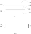
- the optical bonding apparatus 30 includes a pressure sensitive bonding layer 310 and a thermal flow pressure sensitive bonding layer 320 for bonding to a rough surface of an object (not shown).
- the thermal flow pressure sensitive bonding layer 320 is superposed on the pressure sensitive bonding layer 310.
- the pressure sensitive bonding layer 310 has a first surface 312 and a second surface 314.
- the thermal flow pressure sensitive bonding layer 320 has a third surface 322 and a forth surface 324.
- the pressure sensitive bonding layer 310 is superposed on the thermal flow pressure sensitive bonding layer 320 with the first surface 312 and the third surface 322 facing each other and bonding together, making the optical bonding apparatus 30 as a double-layered structure.
- the forth surface 324 is used for bonding to the rough surface of the object (not shown).
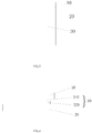
- FIG.3 shows a top view of a touch sensitive display using the optical bonding apparatus 30 of the first embodiment.
- FIG.4 shows a side view of the touch sensitive display using the optical bonding apparatus 30 of the first embodiment.
- the optical bonding apparatus 30 can be applied to the touch sensitive display.
- the touch sensitive display includes a touch panel 10 and an LCD panel 20 facing the touch panel 10.
- the optical bonding apparatus 30 is placed between the touch panel 10 and the LCD panel 20 for bonding the touch panel 10 and the LCD panel 20.
- the LCD panel 20 is the above mentioned object with a rough surface, and the fourth surface 324 of the thermal flow pressure sensitive bonding layer 320 bonds to the rough surface of the LCD panel 20.
- the touch panel 10 is the above mentioned object with a rough surface.
- the optical bonding apparatus 30 is placed between the touch panel 10 and the LCD panel 20 for bonding the touch panel 10 and the LCD panel 20, wherein the fourth surface 324 of the thermal flow pressure sensitive bonding layer 320 bonds to the rough surface of the touch panel 10.
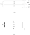
- FIG.5 shows a side view of an optical bonding apparatus with multiple layer structure according to a second embodiment of the present invention.
- the optical bonding apparatus 40 includes a pressure sensitive bonding layer 410, a thermal flow pressure sensitive bonding layer 420 for bonding to a rough surface of an object (not shown), and an organic substrate 430 placed between the pressure sensitive bonding layer 410 and the thermal flow pressure sensitive bonding layer 420. Two surfaces of the organic substrate 430 adhere to the pressure sensitive bonding layer 410 and the thermal flow pressure sensitive bonding layer 420 respectively, making the optical bonding apparatus 40 as a triple-layered structure.
- the pressure sensitive bonding layer 410 has a first surface 412 and a second surface 414
- the thermal flow pressure sensitive bonding layer 420 has a third surface 422 and a forth surface 424.
- the two surfaces of the organic substrate 430 adhere to the first surface 412 and the third surface 422 respectively, making the optical bonding apparatus 40 a triple-layered structure.
- the forth surface 424 of the thermal flow pressure sensitive bonding layer 420 is used for bonding to the rough surface of the object (not shown).
- FIG.6 shows a side view of a touch sensitive display according to the second embodiment of the optical bonding apparatus 40.
- the optical bonding apparatus 40 can be applied to a touch sensitive display which includes a touch panel 10 and an LCD panel 20 facing the touch panel 10.
- the optical bonding apparatus 40 is placed between the touch panel 10 and the LCD panel 20 for bonding the touch panel 10 and the LCD panel 20.
- the LCD panel 20 is the above mentioned object with a rough surface, and the fourth surface 424 bonds to the rough surface of the LCD panel 20.
- the touch panel 10 is the above mentioned object with a rough surface.
- the optical bonding apparatus 40 is placed between the touch panel 10 and the LCD panel 20 for bonding the touch panel 10 and the LCD panel 20.
- the fourth surface 424 bonds to the rough surface of the touch panel 10.
- the second embodiment reduces the thickness of the pressure sensitive bonding layer 410 and improves the die cutting feature (Die cutting is a manufacturing process used to generate large numbers of the same shape from a material such as wood, plastic, metal, or fabric.) of the optical bonding apparatus 40 by placing an organic substrate 430 between the pressure sensitive bonding layer 410 and the thermal flow pressure sensitive bonding layer 420.
- the thickness of the organic substrate 430 is 25 ⁇ m to 100 ⁇ m, and the thickness of the pressure sensitive bonding layer 410 is 25 ⁇ m to 50 ⁇ m.
- the material of the organic substrate 430 is polyethylene terephthalate, or the like.
- the above mentioned pressure sensitive bonding layer and the thermal flow pressure sensitive bonding layer are both transparent in order to keep a better perspectivity while bonding to the touch sensitive display, and both surfaces of the pressure sensitive bonding layer and the thermal flow pressure sensitive bonding layer are adhesive.
- the thermal flow pressure sensitive bonding layer is selected from the group consisting of thermoplastic type, thermal set type and thermal flow type.
- thermoplastic type material has no viscidity or low viscidity while being in solid state at room temperature, and when it turns into liquid state, it has higher viscidity without changing its chemical feature when the temperature goes up to a certain value; it will return to solid state when the temperature comes down, and also it would turn into liquid state again if the temperature goes up again.
- the glass cement is the material of this kind.
- the thermal set type material is in solid state at room temperature, and it turns into liquid state and has higher viscidity as the temperature goes up to a certain value, while its chemical feature also changes. It would return to solid state as the temperature comes down, but it will no longer change into liquid state again even if the temperature goes up again.
- the anisotropic conductive film (ACF) is the material of this kind.
- the thermal flow type material is in solid state at room temperature, and it turns into half-liquid, half-solid state and has higher viscidity as the temperature goes up to a certain value, while its chemical feature also changes. It can return to solid state by adopting additional process such as ultraviolet (UV) solidifying, heating solidifying, vacuum anaerobic solidifying and moisture solidifying.
- UV ultraviolet
- the thermal flow pressure sensitive bonding layer By adopting a heating process, it is easier to bond the thermal flow pressure sensitive bonding layer to the rough surface of the object and to cover the object completely. Because of the feature of the thermal flow pressure sensitive bonding layer, the rough surface can be filled to be flat, which makes the distance between the LCD panel and the touch panel even, as a result reducing or eliminating the development of the mura phenomenon.
- the above mentioned pressure sensitive bonding layers 310, 410 have viscidity while being in solid state at room temperature, and it is very sensitive to pressure. It can bond to the surface of a substrate while being pressed without heating process, and it bonds tighter as the pressure increases.
- a method for producing an optical bonding apparatus is provided as well.
- the method includes the steps as defined in claim 1
- a method for assembling a display device includes the following steps: producing an optical bonding apparatus having a pressure sensitive bonding layer and a thermal flow pressure sensitive bonding layer bonded together, and placing the optical bonding apparatus between a touch panel and an LCD. More detailed processes of above method include: laminating the thermal flow pressure sensitive bonding layer on the rough surface of the touch panel; laminating the pressure sensitive bonding layer on the thermal flow pressure sensitive bonding layer; laminating the LCD panel on the pressure sensitive bonding layer. The three processes of laminating may be processed in any sequence. In another detailed processes of above method include: laminating the thermal flow pressure sensitive bonding layer on the rough surface of the LCD panel; laminating the pressure sensitive bonding layer on the thermal flow pressure sensitive bonding layer; laminating the LCD panel on the pressure sensitive bonding layer.
- the processes of laminating are processed at room temperature, there may be bubbles between layers after each laminating, so a process of auto-claving is added after each process of laminating. In other embodiments, the process of auto-claving is added after the whole three processes of laminating.
- the three processes of laminating are processed at 60°C ⁇ 85°C, which prevents generating bubbles in the process of laminating in a great extent.
- a step of heating the lamination is needed to melt the thermal flow pressure sensitive bonding layer, so that the thermal flow pressure sensitive bonding layer can fill the rough surface of the touch panel or the LCD to be flat.
- the heating time is about 20 minutes to 1 hour depending on the heating temperature.
- a step of solidifying the lamination is added.
- the solidifying process is implemented by exposing the lamination to ultra violet lights, the exposing energy depends on the feature of the bonding layer, and is generally 3000mj.
- the pressure sensitive bonding layer and the thermal flow pressure sensitive bonding layer are bonded together by an organic substrate.
Landscapes
- Physics & Mathematics (AREA)
- Chemical & Material Sciences (AREA)
- Organic Chemistry (AREA)
- Engineering & Computer Science (AREA)
- Nonlinear Science (AREA)
- General Physics & Mathematics (AREA)
- General Engineering & Computer Science (AREA)
- Theoretical Computer Science (AREA)
- Optics & Photonics (AREA)
- Mathematical Physics (AREA)
- Crystallography & Structural Chemistry (AREA)
- Human Computer Interaction (AREA)
- Chemical Kinetics & Catalysis (AREA)
- Position Input By Displaying (AREA)
- Liquid Crystal (AREA)
- Laminated Bodies (AREA)
- Adhesives Or Adhesive Processes (AREA)
- Adhesive Tapes (AREA)
Description
- The present invention generally relates to a method for producing an optical bonding apparatus
- A liquid crystal display (LCD) is a thin, flat electronic visual display that uses the light modulating properties of liquid crystals (LCs). LCs do not emit light directly. Generally, an LCD apparatus includes a display substrate, a liquid crystal drive substrate and a liquid crystal apparatus sealed between the display side substrate and the liquid crystal drive side substrate. For the liquid crystal display apparatus, the display is carried out by electrically controlling the liquid crystal drive side substrate to change the amount of transmitted light from the light source.
- The gap between the display side substrate and the liquid crystal drive side substrate is filled with LCs. As a result, the thickness of the gap is the same as the thickness of the liquid crystal layer.
- T he distance between the display side substrate and the liquid crystal drive side substrate may have inconsisten cies. Such inconsistency will cause the existence of stress in the LCD when the LCs are sealed in the gap. The stress will lead to the variation of the thickness of the liquid crystal layer. As a result, a mura condition develops .
- Mura is the phenomenon described as follows: when an LCD is illuminated , an uneven color line or a color block may be appear on the LCD screen . The color line or the color block is yellow when the background is white, and the color line or the color block is white when the background is gray.
- Generally, the LCD technology is combined with touch sensitive technology to provide easy input to a given system . A touch sensitive display device generally includes an LCD and a transparent touch panel placed thereon. The distance between the LCD and the touch panel cannot be guaranteed to be even, which will amplify the stress, and at the same time increase the chance of mura condition .
- In order to reduce or eliminate the development of the mura phenomenon, an optical bonding apparatus with multiple layer structure, a method for producing the same, and a touch sensitive display using the same are provided.
- An optical bonding apparatus with multiple layer structure includes a pressure sensitive bonding layer and a thermal flow pressure sensitive bonding layer. The thermal flow pressure sensitive bonding layer is used for bonding to a rough surface of an object and superposing on the pressure sensitive bonding layer.
- An optical bonding apparatus with multiple layer structure includes a pressure sensitive bonding layer, a thermal flow pressure sensitive bonding layer, and an organic substrate. The thermal flow pressure sensitive bonding layer is used for bonding to a rough surface of an object and superposing on the pressure sensitive bonding layer. The organic substrate is placed between the pressure sensitive bonding layer and the thermal flow pressure sensitive bonding layer. Two surfaces of the organic substrate bond to the pressure sensitive bonding layer and the thermal flow pressure sensitive bonding layer respectively.
- A method for producing an optical bonding apparatus includes the steps as defined in claim 1
- A method for assembling a display device includes the following steps: producing an optical bonding composition with a pressure sensitive bonding layer and a thermal flow pressure sensitive bonding layer bonded together, and placing the optical bonding composition between a touch panel and an LCD.
- A touch sensitive display includes a touch panel, an LCD panel facing the touch panel, and an above mentioned optical bonding apparatus being placed between the touch panel and the LCD panel for bonding the touch panel and the LCD panel. The thermal flow pressure sensitive bonding layer is bonded to the rough surface of the LCD panel or of the touch panel.
-
US 2004/0191509 A1 discloses a double sided pressure sensitive adhesive sheet that comprises an acrylic pressure sensitive adhesive layer in a touch panel side of the sheet and an acrylic pressure sensitive adhesive layer in a display device side of the sheet, thereby forming a two-layer construction. -
JP 2009 227826 A -
US 2005/233139 A1 describes the use of pressure sensitive adhesives based on acrylate, natural rubber, synthetic rubber or ethyl-vinyl-acetate in a process for preparing a pressure sensitive adhesive using a coolable roll. -
US 2008/1280037 A1 discloses a multilayer assembly that includes a silicon-based multilayer pressure sensitive adhesive article. -
EP 1 835 003 A2 describes a double-faced pressure sensitive adhesive tape or sheet that comprises a pressure sensitive adhesive layer disposed on a base material, wherein the pressure sensitive adhesive layer includes a pressure sensitive adhesive composition that contains an acrylic polymer and a silicon rubber fine particle, and a further pressure sensitive adhesive layer that also includes an acrylic polymer and fiber includes a low molecular weight polymer component. - A double-sided, self-adhesive reinforced foam tape is known from
WO 01/156777 A1 -
-
FIG.1 shows an exploded view of an optical bonding apparatus with multiple layer structure in accordance with a first preferred embodiment of the present invention. -
FIG.2 shows a side view of an optical bonding apparatus with multiple layer structure in accordance with the first preferred embodiment of the present invention. -
FIG.3 shows a top view of the touch sensitive display using the optical bonding apparatus with multiple layer structure in accordance with a preferred embodiment of the present invention. -
FIG.4 shows a side view of a touch sensitive display using the optical bonding apparatus with multiple layer structure in accordance with a first preferred embodiment of the present invention. -
FIG.5 shows a side view of an optical bonding apparatus with multiple layer structure in accordance with a second preferred embodiment of the present invention. -
FIG.6 shows a side view of a touch sensitive display using the optical bonding apparatus with multiple layer structure in accordance with the second preferred embodiment of the present invention. - The detailed description of the present invention will be discussed in the following embodiments, which are not intended to limit the scope of the present invention, but still can be adapted for other applications. While drawings are illustrated in details, it is appreciated that the quantity of the disclosed components could be greater or less than that disclosed, except those components with expressly restricting amount.
- Referring to
FIG.1 and FIG.2 , an exploded view and side view of an optical bonding apparatus with multiple layer structure are shown respectively according to a first embodiment of the present invention. Theoptical bonding apparatus 30 includes a pressuresensitive bonding layer 310 and a thermal flow pressuresensitive bonding layer 320 for bonding to a rough surface of an object (not shown). The thermal flow pressuresensitive bonding layer 320 is superposed on the pressuresensitive bonding layer 310. - The pressure
sensitive bonding layer 310 has afirst surface 312 and asecond surface 314. The thermal flow pressuresensitive bonding layer 320 has athird surface 322 and a forthsurface 324. The pressuresensitive bonding layer 310 is superposed on the thermal flow pressuresensitive bonding layer 320 with thefirst surface 312 and thethird surface 322 facing each other and bonding together, making theoptical bonding apparatus 30 as a double-layered structure. Theforth surface 324 is used for bonding to the rough surface of the object (not shown). -
FIG.3 shows a top view of a touch sensitive display using theoptical bonding apparatus 30 of the first embodiment.FIG.4 shows a side view of the touch sensitive display using theoptical bonding apparatus 30 of the first embodiment. Theoptical bonding apparatus 30 can be applied to the touch sensitive display. The touch sensitive display includes atouch panel 10 and anLCD panel 20 facing thetouch panel 10. Theoptical bonding apparatus 30 is placed between thetouch panel 10 and theLCD panel 20 for bonding thetouch panel 10 and theLCD panel 20. In a preferred embodiment, theLCD panel 20 is the above mentioned object with a rough surface, and thefourth surface 324 of the thermal flow pressuresensitive bonding layer 320 bonds to the rough surface of theLCD panel 20. - In an alternative embodiment, the
touch panel 10 is the above mentioned object with a rough surface. Theoptical bonding apparatus 30 is placed between thetouch panel 10 and theLCD panel 20 for bonding thetouch panel 10 and theLCD panel 20, wherein thefourth surface 324 of the thermal flow pressuresensitive bonding layer 320 bonds to the rough surface of thetouch panel 10. -
FIG.5 shows a side view of an optical bonding apparatus with multiple layer structure according to a second embodiment of the present invention. In this embodiment, theoptical bonding apparatus 40 includes a pressuresensitive bonding layer 410, a thermal flow pressuresensitive bonding layer 420 for bonding to a rough surface of an object (not shown), and anorganic substrate 430 placed between the pressuresensitive bonding layer 410 and the thermal flow pressuresensitive bonding layer 420. Two surfaces of theorganic substrate 430 adhere to the pressuresensitive bonding layer 410 and the thermal flow pressuresensitive bonding layer 420 respectively, making theoptical bonding apparatus 40 as a triple-layered structure. - The pressure
sensitive bonding layer 410 has a first surface 412 and asecond surface 414, the thermal flow pressuresensitive bonding layer 420 has athird surface 422 and aforth surface 424. The two surfaces of theorganic substrate 430 adhere to the first surface 412 and thethird surface 422 respectively, making the optical bonding apparatus 40 a triple-layered structure. Theforth surface 424 of the thermal flow pressuresensitive bonding layer 420 is used for bonding to the rough surface of the object (not shown). -
FIG.6 shows a side view of a touch sensitive display according to the second embodiment of theoptical bonding apparatus 40. Theoptical bonding apparatus 40 can be applied to a touch sensitive display which includes atouch panel 10 and anLCD panel 20 facing thetouch panel 10. Theoptical bonding apparatus 40 is placed between thetouch panel 10 and theLCD panel 20 for bonding thetouch panel 10 and theLCD panel 20. In a preferred embodiment, theLCD panel 20 is the above mentioned object with a rough surface, and thefourth surface 424 bonds to the rough surface of theLCD panel 20. - In an alternative embodiment, the
touch panel 10 is the above mentioned object with a rough surface. Theoptical bonding apparatus 40 is placed between thetouch panel 10 and theLCD panel 20 for bonding thetouch panel 10 and theLCD panel 20. Thefourth surface 424 bonds to the rough surface of thetouch panel 10. - The second embodiment reduces the thickness of the pressure
sensitive bonding layer 410 and improves the die cutting feature (Die cutting is a manufacturing process used to generate large numbers of the same shape from a material such as wood, plastic, metal, or fabric.) of theoptical bonding apparatus 40 by placing anorganic substrate 430 between the pressuresensitive bonding layer 410 and the thermal flow pressuresensitive bonding layer 420. The thickness of theorganic substrate 430 is 25µm to 100µm, and the thickness of the pressuresensitive bonding layer 410 is 25µm to 50µm. In a preferred embodiment, the material of theorganic substrate 430 is polyethylene terephthalate, or the like. - The above mentioned pressure sensitive bonding layer and the thermal flow pressure sensitive bonding layer are both transparent in order to keep a better perspectivity while bonding to the touch sensitive display, and both surfaces of the pressure sensitive bonding layer and the thermal flow pressure sensitive bonding layer are adhesive.
- The thermal flow pressure sensitive bonding layer is selected from the group consisting of thermoplastic type, thermal set type and thermal flow type.
- The thermoplastic type material has no viscidity or low viscidity while being in solid state at room temperature, and when it turns into liquid state, it has higher viscidity without changing its chemical feature when the temperature goes up to a certain value; it will return to solid state when the temperature comes down, and also it would turn into liquid state again if the temperature goes up again. The glass cement is the material of this kind.
- The thermal set type material is in solid state at room temperature, and it turns into liquid state and has higher viscidity as the temperature goes up to a certain value, while its chemical feature also changes. It would return to solid state as the temperature comes down, but it will no longer change into liquid state again even if the temperature goes up again. The anisotropic conductive film (ACF) is the material of this kind.
- The thermal flow type material is in solid state at room temperature, and it turns into half-liquid, half-solid state and has higher viscidity as the temperature goes up to a certain value, while its chemical feature also changes. It can return to solid state by adopting additional process such as ultraviolet (UV) solidifying, heating solidifying, vacuum anaerobic solidifying and moisture solidifying.
- By adopting a heating process, it is easier to bond the thermal flow pressure sensitive bonding layer to the rough surface of the object and to cover the object completely. Because of the feature of the thermal flow pressure sensitive bonding layer, the rough surface can be filled to be flat, which makes the distance between the LCD panel and the touch panel even, as a result reducing or eliminating the development of the mura phenomenon.
- The above mentioned pressure sensitive bonding layers 310, 410 have viscidity while being in solid state at room temperature, and it is very sensitive to pressure. It can bond to the surface of a substrate while being pressed without heating process, and it bonds tighter as the pressure increases.
- A method for producing an optical bonding apparatus is provided as well. The method includes the steps as defined in claim 1
- In addition, a method for assembling a display device is provided. The method includes the following steps: producing an optical bonding apparatus having a pressure sensitive bonding layer and a thermal flow pressure sensitive bonding layer bonded together, and placing the optical bonding apparatus between a touch panel and an LCD. More detailed processes of above method include: laminating the thermal flow pressure sensitive bonding layer on the rough surface of the touch panel; laminating the pressure sensitive bonding layer on the thermal flow pressure sensitive bonding layer; laminating the LCD panel on the pressure sensitive bonding layer. The three processes of laminating may be processed in any sequence. In another detailed processes of above method include: laminating the thermal flow pressure sensitive bonding layer on the rough surface of the LCD panel; laminating the pressure sensitive bonding layer on the thermal flow pressure sensitive bonding layer; laminating the LCD panel on the pressure sensitive bonding layer.
- If the processes of laminating are processed at room temperature, there may be bubbles between layers after each laminating, so a process of auto-claving is added after each process of laminating. In other embodiments, the process of auto-claving is added after the whole three processes of laminating.
- In a preferred embodiment, the three processes of laminating are processed at 60°C~85°C, which prevents generating bubbles in the process of laminating in a great extent.
- After the above processes, a step of heating the lamination is needed to melt the thermal flow pressure sensitive bonding layer, so that the thermal flow pressure sensitive bonding layer can fill the rough surface of the touch panel or the LCD to be flat. The heating time is about 20 minutes to 1 hour depending on the heating temperature. When the rough surface is filled to be flat and the distance between the LCD panel and the touch panel is even, a step of solidifying the lamination is added. The solidifying process is implemented by exposing the lamination to ultra violet lights, the exposing energy depends on the feature of the bonding layer, and is generally 3000mj.
- In other embodiments, the pressure sensitive bonding layer and the thermal flow pressure sensitive bonding layer are bonded together by an organic substrate.
Claims (6)
- A method comprising:producing an optical bonding apparatus (30; 40) with at least a pressure sensitive bonding layer (310; 410) and a thermal flow pressure sensitive bonding layer (320; 420) bonded together; andplacing the optical bonding apparatus (30; 40) between a touch panel (10) and an LCD panel (20), wherein the material of the thermal flow pressure sensitive bonding layer (320; 420) is a thermal flow type;wherein the detailed processes comprise:laminating the thermal flow pressure sensitive bonding layer (320; 420) on the rough surface of the touch panel;laminating the pressure sensitive bonding layer on the thermal flow pressure sensitive bonding layer; andlaminating the LCD panel on the pressure sensitive bonding layer;wherein the method further comprises a process of auto-claving after each process of laminating.
- The method according to claim 1, wherein the three processes of laminating are processed at 60°C~85°C.
- The method according to claim 2, further comprising a step of heating the lamination.
- The method according to claim 3, further comprising a step of solidifying the laminations by exposing the lamination to ultra violet lights.
- The method according to claim 4, wherein the exposing energy is 3000 mJ.
- The method according to claim 1, wherein the pressure sensitive bonding layer and the thermal flow pressure sensitive bonding layer are bonded together by an organic substrate.
Applications Claiming Priority (2)
| Application Number | Priority Date | Filing Date | Title |
|---|---|---|---|
| CN201010130377.0A CN102190972B (en) | 2010-03-14 | 2010-03-14 | Optical adhesive layer with multilayer structure |
| PCT/CN2010/076655 WO2011113263A1 (en) | 2010-03-14 | 2010-09-07 | Multilayer structure, method for producing the same and touch sensitive display using the same |
Publications (3)
| Publication Number | Publication Date |
|---|---|
| EP2547742A1 EP2547742A1 (en) | 2013-01-23 |
| EP2547742A4 EP2547742A4 (en) | 2017-10-18 |
| EP2547742B1 true EP2547742B1 (en) | 2021-06-23 |
Family
ID=44599872
Family Applications (1)
| Application Number | Title | Priority Date | Filing Date |
|---|---|---|---|
| EP10847732.4A Active EP2547742B1 (en) | 2010-03-14 | 2010-09-07 | Multilayer structure, method for producing the same and touch sensitive display using the same |
Country Status (6)
| Country | Link |
|---|---|
| US (1) | US10558071B2 (en) |
| EP (1) | EP2547742B1 (en) |
| JP (1) | JP5750125B2 (en) |
| KR (1) | KR101663857B1 (en) |
| CN (1) | CN102190972B (en) |
| WO (1) | WO2011113263A1 (en) |
Families Citing this family (9)
| Publication number | Priority date | Publication date | Assignee | Title |
|---|---|---|---|---|
| CN102792218B (en) | 2010-03-09 | 2016-02-03 | 3M创新有限公司 | For bonding the thermal activation optically clear adhesive of display panel |
| KR101990537B1 (en) * | 2012-07-27 | 2019-06-19 | 삼성디스플레이 주식회사 | Window structure for protecting a display panel, display panel assembly including the same, method of manufacturing a window structure for protecting a display panel and method of manufacturing a display panel assembly using the same |
| US9128674B2 (en) * | 2012-09-07 | 2015-09-08 | Apple Inc. | Thermal press and ultraviolet curing for display assemblies |
| TWI645009B (en) * | 2013-05-10 | 2018-12-21 | 王子控股股份有限公司 | Laminated adhesive sheets and laminated bodies |
| US10521181B2 (en) | 2013-06-28 | 2019-12-31 | Amazon Technologies, Inc. | Reducing discoloration of a display stack |
| TW201535180A (en) * | 2014-03-13 | 2015-09-16 | Henghao Technology Co Ltd | Touch panel and method of attaching same |
| CN109656321A (en) * | 2018-11-30 | 2019-04-19 | 深圳全息界科技有限公司 | A kind of display heat cure attaching process and display |
| CN110673372A (en) * | 2019-09-30 | 2020-01-10 | 京东方科技集团股份有限公司 | A kind of double-sided adhesive tape and display device |
| CN110669445A (en) * | 2019-09-30 | 2020-01-10 | 东莞晶邦光电科技有限公司 | Optical laminating adhesive, display screen assembly and preparation method thereof |
Citations (1)
| Publication number | Priority date | Publication date | Assignee | Title |
|---|---|---|---|---|
| US5990267A (en) * | 1995-05-03 | 1999-11-23 | Alcatel Cable | Optical fibre and optical fibre tape, and method for making same |
Family Cites Families (19)
| Publication number | Priority date | Publication date | Assignee | Title |
|---|---|---|---|---|
| US5478639A (en) * | 1993-05-12 | 1995-12-26 | Teraoka Seisakusho Co., Ltd. | Adhesive tape for preventing implosion of cathode ray tube |
| JPH11348068A (en) * | 1998-06-08 | 1999-12-21 | Nissha Printing Co Ltd | Insert film with pressure sensitive adhesive and manufacture of molding with pressure sensitive adhesive |
| JP4213792B2 (en) * | 1998-09-24 | 2009-01-21 | 日東電工株式会社 | Thermosetting pressure-sensitive adhesive and its adhesive sheets |
| US6451398B1 (en) * | 1998-11-24 | 2002-09-17 | Michael S. Sylvester | Double-sided self-adhesive reinforced foam tape |
| JP3880418B2 (en) * | 2002-02-21 | 2007-02-14 | 日東電工株式会社 | Method for sticking and fixing double-sided adhesive sheet and touch panel to display device |
| DE10221092A1 (en) * | 2002-05-11 | 2003-12-11 | Tesa Ag | Foamed PSAs |
| CN100367428C (en) * | 2002-09-03 | 2008-02-06 | 日本写真印刷株式会社 | Touch screen with adhesive layer |
| JP4493273B2 (en) * | 2003-01-29 | 2010-06-30 | 日東電工株式会社 | Double-sided adhesive sheet and display device with touch panel |
| DE102005027393A1 (en) * | 2005-06-13 | 2006-12-21 | Tesa Ag | Double-sided pressure-sensitive adhesive tapes for the production of LC displays with light-reflecting and absorbing properties |
| JP5085145B2 (en) * | 2006-03-15 | 2012-11-28 | 日東電工株式会社 | Double-sided adhesive tape or sheet and liquid crystal display device |
| JP2008027329A (en) * | 2006-07-25 | 2008-02-07 | Matsushita Electric Ind Co Ltd | Touch panel |
| JP4614003B2 (en) * | 2006-08-29 | 2011-01-19 | 日立化成工業株式会社 | Anisotropic conductive tape, method for manufacturing the same, connection structure using the same, and method for connecting circuit members |
| US7833577B2 (en) | 2007-05-11 | 2010-11-16 | 3M Innovative Properties Company | Methods of making a pressure-sensitive adhesive assembly |
| US8134540B2 (en) * | 2007-10-16 | 2012-03-13 | Wintek Corporation | Touch panel and liquid crystal display panel |
| US20090110861A1 (en) * | 2007-10-29 | 2009-04-30 | 3M Innovative Properties Company | Pressure sensitive adhesive article |
| JP5428158B2 (en) * | 2007-12-27 | 2014-02-26 | Dic株式会社 | Double-sided adhesive tape |
| JP2009227826A (en) * | 2008-03-24 | 2009-10-08 | Dic Corp | Double coated self-adhesive tape and image display module |
| CN102792218B (en) * | 2010-03-09 | 2016-02-03 | 3M创新有限公司 | For bonding the thermal activation optically clear adhesive of display panel |
| CN201662668U (en) * | 2010-03-14 | 2010-12-01 | 宸鸿科技(厦门)有限公司 | Multilayered structural optical bonding course |
-
2010
- 2010-03-14 CN CN201010130377.0A patent/CN102190972B/en not_active Expired - Fee Related
- 2010-09-07 US US13/634,918 patent/US10558071B2/en active Active
- 2010-09-07 JP JP2012557376A patent/JP5750125B2/en not_active Expired - Fee Related
- 2010-09-07 WO PCT/CN2010/076655 patent/WO2011113263A1/en not_active Ceased
- 2010-09-07 KR KR1020127026800A patent/KR101663857B1/en not_active Expired - Fee Related
- 2010-09-07 EP EP10847732.4A patent/EP2547742B1/en active Active
Patent Citations (1)
| Publication number | Priority date | Publication date | Assignee | Title |
|---|---|---|---|---|
| US5990267A (en) * | 1995-05-03 | 1999-11-23 | Alcatel Cable | Optical fibre and optical fibre tape, and method for making same |
Non-Patent Citations (1)
| Title |
|---|
| DONALD V ROSATO ET AL: "Passage; Concise Encyclopedia of Plastics", 1 January 2000, CONCISE ENCYCLOPEDIA OF PLASTICS, KLUWER ACAD. PUBL, BOSTON, MASS, PAGE(S) 526 - 530, ISBN: 978-0-7923-8496-0, XP009521565 * |
Also Published As
| Publication number | Publication date |
|---|---|
| JP2013522398A (en) | 2013-06-13 |
| US20130033458A1 (en) | 2013-02-07 |
| JP5750125B2 (en) | 2015-07-15 |
| EP2547742A4 (en) | 2017-10-18 |
| CN102190972B (en) | 2014-01-29 |
| EP2547742A1 (en) | 2013-01-23 |
| WO2011113263A1 (en) | 2011-09-22 |
| US10558071B2 (en) | 2020-02-11 |
| KR20120135320A (en) | 2012-12-12 |
| CN102190972A (en) | 2011-09-21 |
| KR101663857B1 (en) | 2016-10-07 |
Similar Documents
| Publication | Publication Date | Title |
|---|---|---|
| US10558071B2 (en) | Multilayer structure, method for producing the same and touch sensitive display using the same | |
| TWI425288B (en) | Electro-optic displays with color filters | |
| US7583427B2 (en) | Components and methods for use in electro-optic displays | |
| CN202372959U (en) | Optical bonding structure and touch display | |
| WO2005072447A3 (en) | Liquid crystal display films | |
| CN107545848A (en) | Flexible cover plate and preparation method thereof, flexible OLED display | |
| WO2005072455A3 (en) | Drapable liquid crystal transfer display films | |
| TW200726993A (en) | Optical film composite having spatially controlled adhesion | |
| KR20160044162A (en) | Manufacturing method of flexible display device | |
| EP2161616A8 (en) | Double-layer liquid crystal lens and method for manufacturing the same | |
| US20120275024A1 (en) | Polarizer assembly with adhesive layers | |
| JPWO2014061607A1 (en) | Transparent surface material with adhesive layer, display device, and manufacturing method thereof | |
| WO2009047933A1 (en) | Light control layer of backlight, backlight, liquid crystal display, and method of manufacturing light control layer of backlight | |
| US10884515B2 (en) | Lamination method of substrates and product prepared thereby | |
| CN104267456A (en) | Polarizer, display panel, display panel forming method and display device | |
| EP2886331B1 (en) | Laminate comprising adhesive layer and method for manufacturing same | |
| CN108511504A (en) | The manufacturing method of display module and display module | |
| EP3605216B1 (en) | Glue sealing method for display screen frame | |
| CN105425449A (en) | Touch liquid crystal display device and electronic equipment | |
| TW200643521A (en) | Double-side adhesive bands for the production or adhesion of LC-display with light-absorbent property | |
| WO2014117333A1 (en) | Display devices and methods of assembly | |
| WO2013016859A1 (en) | Layered display device and fabrication method thereof | |
| TW200738452A (en) | Method for manufacturing surface protection board for liquid crystal display device and method for manufacturing liquid crystal display device | |
| WO2009020043A1 (en) | Adhesive tape for display device assembly, and display module unit using adhesive tape | |
| TW200622357A (en) | Display panel and liquid crystal display device |
Legal Events
| Date | Code | Title | Description |
|---|---|---|---|
| PUAI | Public reference made under article 153(3) epc to a published international application that has entered the european phase |
Free format text: ORIGINAL CODE: 0009012 |
|
| 17P | Request for examination filed |
Effective date: 20121009 |
|
| AK | Designated contracting states |
Kind code of ref document: A1 Designated state(s): AL AT BE BG CH CY CZ DE DK EE ES FI FR GB GR HR HU IE IS IT LI LT LU LV MC MK MT NL NO PL PT RO SE SI SK SM TR |
|
| RIN1 | Information on inventor provided before grant (corrected) |
Inventor name: YUAN, QIONG Inventor name: XU, XIANBIN Inventor name: LIN, FENGMING Inventor name: LEE, YUHWEN |
|
| DAX | Request for extension of the european patent (deleted) | ||
| RIN1 | Information on inventor provided before grant (corrected) |
Inventor name: XU, XIANBIN Inventor name: LIN, FENGMING Inventor name: YUAN, QIONG Inventor name: LEE, YUHWEN |
|
| RIN1 | Information on inventor provided before grant (corrected) |
Inventor name: XU, XIANBIN Inventor name: YUAN, QIONG Inventor name: LEE, YUHWEN Inventor name: LIN, FENGMING |
|
| RIN1 | Information on inventor provided before grant (corrected) |
Inventor name: LEE, YUHWEN Inventor name: XU, XIANBIN Inventor name: LIN, FENGMING Inventor name: YUAN, QIONG |
|
| RIC1 | Information provided on ipc code assigned before grant |
Ipc: C09J 7/02 20060101ALI20170601BHEP Ipc: C09J 7/00 20060101AFI20170601BHEP |
|
| RA4 | Supplementary search report drawn up and despatched (corrected) |
Effective date: 20170919 |
|
| RIC1 | Information provided on ipc code assigned before grant |
Ipc: C09J 7/02 20060101ALI20170913BHEP Ipc: C09J 7/00 20060101AFI20170913BHEP Ipc: G02F 1/1333 20060101ALI20170913BHEP |
|
| STAA | Information on the status of an ep patent application or granted ep patent |
Free format text: STATUS: EXAMINATION IS IN PROGRESS |
|
| 17Q | First examination report despatched |
Effective date: 20180829 |
|
| REG | Reference to a national code |
Ref country code: DE Ref legal event code: R079 Ref document number: 602010067171 Country of ref document: DE Free format text: PREVIOUS MAIN CLASS: C09J0007020000 Ipc: C09J0007100000 |
|
| RIC1 | Information provided on ipc code assigned before grant |
Ipc: C09J 7/22 20180101ALI20201201BHEP Ipc: C09J 7/38 20180101ALI20201201BHEP Ipc: C09J 7/10 20180101AFI20201201BHEP Ipc: G02F 1/1333 20060101ALI20201201BHEP |
|
| GRAP | Despatch of communication of intention to grant a patent |
Free format text: ORIGINAL CODE: EPIDOSNIGR1 |
|
| STAA | Information on the status of an ep patent application or granted ep patent |
Free format text: STATUS: GRANT OF PATENT IS INTENDED |
|
| INTG | Intention to grant announced |
Effective date: 20210203 |
|
| RAP1 | Party data changed (applicant data changed or rights of an application transferred) |
Owner name: TPK TOUCH SOLUTIONS (XIAMEN) INC. |
|
| GRAS | Grant fee paid |
Free format text: ORIGINAL CODE: EPIDOSNIGR3 |
|
| GRAA | (expected) grant |
Free format text: ORIGINAL CODE: 0009210 |
|
| STAA | Information on the status of an ep patent application or granted ep patent |
Free format text: STATUS: THE PATENT HAS BEEN GRANTED |
|
| AK | Designated contracting states |
Kind code of ref document: B1 Designated state(s): AL AT BE BG CH CY CZ DE DK EE ES FI FR GB GR HR HU IE IS IT LI LT LU LV MC MK MT NL NO PL PT RO SE SI SK SM TR |
|
| REG | Reference to a national code |
Ref country code: GB Ref legal event code: FG4D |
|
| REG | Reference to a national code |
Ref country code: CH Ref legal event code: EP |
|
| REG | Reference to a national code |
Ref country code: DE Ref legal event code: R096 Ref document number: 602010067171 Country of ref document: DE Ref country code: AT Ref legal event code: REF Ref document number: 1404304 Country of ref document: AT Kind code of ref document: T Effective date: 20210715 |
|
| REG | Reference to a national code |
Ref country code: IE Ref legal event code: FG4D |
|
| REG | Reference to a national code |
Ref country code: NL Ref legal event code: FP |
|
| REG | Reference to a national code |
Ref country code: LT Ref legal event code: MG9D |
|
| PG25 | Lapsed in a contracting state [announced via postgrant information from national office to epo] |
Ref country code: FI Free format text: LAPSE BECAUSE OF FAILURE TO SUBMIT A TRANSLATION OF THE DESCRIPTION OR TO PAY THE FEE WITHIN THE PRESCRIBED TIME-LIMIT Effective date: 20210623 Ref country code: LT Free format text: LAPSE BECAUSE OF FAILURE TO SUBMIT A TRANSLATION OF THE DESCRIPTION OR TO PAY THE FEE WITHIN THE PRESCRIBED TIME-LIMIT Effective date: 20210623 Ref country code: BG Free format text: LAPSE BECAUSE OF FAILURE TO SUBMIT A TRANSLATION OF THE DESCRIPTION OR TO PAY THE FEE WITHIN THE PRESCRIBED TIME-LIMIT Effective date: 20210923 Ref country code: HR Free format text: LAPSE BECAUSE OF FAILURE TO SUBMIT A TRANSLATION OF THE DESCRIPTION OR TO PAY THE FEE WITHIN THE PRESCRIBED TIME-LIMIT Effective date: 20210623 |
|
| REG | Reference to a national code |
Ref country code: AT Ref legal event code: MK05 Ref document number: 1404304 Country of ref document: AT Kind code of ref document: T Effective date: 20210623 |
|
| PG25 | Lapsed in a contracting state [announced via postgrant information from national office to epo] |
Ref country code: LV Free format text: LAPSE BECAUSE OF FAILURE TO SUBMIT A TRANSLATION OF THE DESCRIPTION OR TO PAY THE FEE WITHIN THE PRESCRIBED TIME-LIMIT Effective date: 20210623 Ref country code: GR Free format text: LAPSE BECAUSE OF FAILURE TO SUBMIT A TRANSLATION OF THE DESCRIPTION OR TO PAY THE FEE WITHIN THE PRESCRIBED TIME-LIMIT Effective date: 20210924 Ref country code: SE Free format text: LAPSE BECAUSE OF FAILURE TO SUBMIT A TRANSLATION OF THE DESCRIPTION OR TO PAY THE FEE WITHIN THE PRESCRIBED TIME-LIMIT Effective date: 20210623 Ref country code: NO Free format text: LAPSE BECAUSE OF FAILURE TO SUBMIT A TRANSLATION OF THE DESCRIPTION OR TO PAY THE FEE WITHIN THE PRESCRIBED TIME-LIMIT Effective date: 20210923 |
|
| PG25 | Lapsed in a contracting state [announced via postgrant information from national office to epo] |
Ref country code: AT Free format text: LAPSE BECAUSE OF FAILURE TO SUBMIT A TRANSLATION OF THE DESCRIPTION OR TO PAY THE FEE WITHIN THE PRESCRIBED TIME-LIMIT Effective date: 20210623 Ref country code: PT Free format text: LAPSE BECAUSE OF FAILURE TO SUBMIT A TRANSLATION OF THE DESCRIPTION OR TO PAY THE FEE WITHIN THE PRESCRIBED TIME-LIMIT Effective date: 20211025 Ref country code: RO Free format text: LAPSE BECAUSE OF FAILURE TO SUBMIT A TRANSLATION OF THE DESCRIPTION OR TO PAY THE FEE WITHIN THE PRESCRIBED TIME-LIMIT Effective date: 20210623 Ref country code: ES Free format text: LAPSE BECAUSE OF FAILURE TO SUBMIT A TRANSLATION OF THE DESCRIPTION OR TO PAY THE FEE WITHIN THE PRESCRIBED TIME-LIMIT Effective date: 20210623 Ref country code: EE Free format text: LAPSE BECAUSE OF FAILURE TO SUBMIT A TRANSLATION OF THE DESCRIPTION OR TO PAY THE FEE WITHIN THE PRESCRIBED TIME-LIMIT Effective date: 20210623 Ref country code: CZ Free format text: LAPSE BECAUSE OF FAILURE TO SUBMIT A TRANSLATION OF THE DESCRIPTION OR TO PAY THE FEE WITHIN THE PRESCRIBED TIME-LIMIT Effective date: 20210623 Ref country code: SK Free format text: LAPSE BECAUSE OF FAILURE TO SUBMIT A TRANSLATION OF THE DESCRIPTION OR TO PAY THE FEE WITHIN THE PRESCRIBED TIME-LIMIT Effective date: 20210623 Ref country code: SM Free format text: LAPSE BECAUSE OF FAILURE TO SUBMIT A TRANSLATION OF THE DESCRIPTION OR TO PAY THE FEE WITHIN THE PRESCRIBED TIME-LIMIT Effective date: 20210623 |
|
| PG25 | Lapsed in a contracting state [announced via postgrant information from national office to epo] |
Ref country code: PL Free format text: LAPSE BECAUSE OF FAILURE TO SUBMIT A TRANSLATION OF THE DESCRIPTION OR TO PAY THE FEE WITHIN THE PRESCRIBED TIME-LIMIT Effective date: 20210623 |
|
| REG | Reference to a national code |
Ref country code: DE Ref legal event code: R097 Ref document number: 602010067171 Country of ref document: DE |
|
| PG25 | Lapsed in a contracting state [announced via postgrant information from national office to epo] |
Ref country code: DK Free format text: LAPSE BECAUSE OF FAILURE TO SUBMIT A TRANSLATION OF THE DESCRIPTION OR TO PAY THE FEE WITHIN THE PRESCRIBED TIME-LIMIT Effective date: 20210623 |
|
| PLBE | No opposition filed within time limit |
Free format text: ORIGINAL CODE: 0009261 |
|
| STAA | Information on the status of an ep patent application or granted ep patent |
Free format text: STATUS: NO OPPOSITION FILED WITHIN TIME LIMIT |
|
| REG | Reference to a national code |
Ref country code: CH Ref legal event code: PL |
|
| REG | Reference to a national code |
Ref country code: BE Ref legal event code: MM Effective date: 20210930 |
|
| 26N | No opposition filed |
Effective date: 20220324 |
|
| PG25 | Lapsed in a contracting state [announced via postgrant information from national office to epo] |
Ref country code: MC Free format text: LAPSE BECAUSE OF FAILURE TO SUBMIT A TRANSLATION OF THE DESCRIPTION OR TO PAY THE FEE WITHIN THE PRESCRIBED TIME-LIMIT Effective date: 20210623 Ref country code: AL Free format text: LAPSE BECAUSE OF FAILURE TO SUBMIT A TRANSLATION OF THE DESCRIPTION OR TO PAY THE FEE WITHIN THE PRESCRIBED TIME-LIMIT Effective date: 20210623 |
|
| PG25 | Lapsed in a contracting state [announced via postgrant information from national office to epo] |
Ref country code: LU Free format text: LAPSE BECAUSE OF NON-PAYMENT OF DUE FEES Effective date: 20210907 Ref country code: IT Free format text: LAPSE BECAUSE OF FAILURE TO SUBMIT A TRANSLATION OF THE DESCRIPTION OR TO PAY THE FEE WITHIN THE PRESCRIBED TIME-LIMIT Effective date: 20210623 Ref country code: IE Free format text: LAPSE BECAUSE OF NON-PAYMENT OF DUE FEES Effective date: 20210907 Ref country code: BE Free format text: LAPSE BECAUSE OF NON-PAYMENT OF DUE FEES Effective date: 20210930 |
|
| PG25 | Lapsed in a contracting state [announced via postgrant information from national office to epo] |
Ref country code: LI Free format text: LAPSE BECAUSE OF NON-PAYMENT OF DUE FEES Effective date: 20210930 Ref country code: CH Free format text: LAPSE BECAUSE OF NON-PAYMENT OF DUE FEES Effective date: 20210930 |
|
| PG25 | Lapsed in a contracting state [announced via postgrant information from national office to epo] |
Ref country code: HU Free format text: LAPSE BECAUSE OF FAILURE TO SUBMIT A TRANSLATION OF THE DESCRIPTION OR TO PAY THE FEE WITHIN THE PRESCRIBED TIME-LIMIT; INVALID AB INITIO Effective date: 20100907 Ref country code: CY Free format text: LAPSE BECAUSE OF FAILURE TO SUBMIT A TRANSLATION OF THE DESCRIPTION OR TO PAY THE FEE WITHIN THE PRESCRIBED TIME-LIMIT Effective date: 20210623 |
|
| PGFP | Annual fee paid to national office [announced via postgrant information from national office to epo] |
Ref country code: NL Payment date: 20230719 Year of fee payment: 14 |
|
| PGFP | Annual fee paid to national office [announced via postgrant information from national office to epo] |
Ref country code: GB Payment date: 20230720 Year of fee payment: 14 |
|
| PGFP | Annual fee paid to national office [announced via postgrant information from national office to epo] |
Ref country code: FR Payment date: 20230703 Year of fee payment: 14 Ref country code: DE Payment date: 20230712 Year of fee payment: 14 |
|
| PG25 | Lapsed in a contracting state [announced via postgrant information from national office to epo] |
Ref country code: MK Free format text: LAPSE BECAUSE OF FAILURE TO SUBMIT A TRANSLATION OF THE DESCRIPTION OR TO PAY THE FEE WITHIN THE PRESCRIBED TIME-LIMIT Effective date: 20210623 |
|
| PG25 | Lapsed in a contracting state [announced via postgrant information from national office to epo] |
Ref country code: MT Free format text: LAPSE BECAUSE OF FAILURE TO SUBMIT A TRANSLATION OF THE DESCRIPTION OR TO PAY THE FEE WITHIN THE PRESCRIBED TIME-LIMIT Effective date: 20210623 |
|
| REG | Reference to a national code |
Ref country code: DE Ref legal event code: R119 Ref document number: 602010067171 Country of ref document: DE |
|
| REG | Reference to a national code |
Ref country code: NL Ref legal event code: MM Effective date: 20241001 |
|
| GBPC | Gb: european patent ceased through non-payment of renewal fee |
Effective date: 20240907 |
|
| PG25 | Lapsed in a contracting state [announced via postgrant information from national office to epo] |
Ref country code: NL Free format text: LAPSE BECAUSE OF NON-PAYMENT OF DUE FEES Effective date: 20241001 |
|
| PG25 | Lapsed in a contracting state [announced via postgrant information from national office to epo] |
Ref country code: DE Free format text: LAPSE BECAUSE OF NON-PAYMENT OF DUE FEES Effective date: 20250401 |
|
| PG25 | Lapsed in a contracting state [announced via postgrant information from national office to epo] |
Ref country code: GB Free format text: LAPSE BECAUSE OF NON-PAYMENT OF DUE FEES Effective date: 20240907 |
|
| PG25 | Lapsed in a contracting state [announced via postgrant information from national office to epo] |
Ref country code: FR Free format text: LAPSE BECAUSE OF NON-PAYMENT OF DUE FEES Effective date: 20240930 |
|
| PG25 | Lapsed in a contracting state [announced via postgrant information from national office to epo] |
Ref country code: TR Free format text: LAPSE BECAUSE OF FAILURE TO SUBMIT A TRANSLATION OF THE DESCRIPTION OR TO PAY THE FEE WITHIN THE PRESCRIBED TIME-LIMIT Effective date: 20210623 |