EP2547181A1 - A protection device for ESD protection - Google Patents
A protection device for ESD protection Download PDFInfo
- Publication number
- EP2547181A1 EP2547181A1 EP11173581A EP11173581A EP2547181A1 EP 2547181 A1 EP2547181 A1 EP 2547181A1 EP 11173581 A EP11173581 A EP 11173581A EP 11173581 A EP11173581 A EP 11173581A EP 2547181 A1 EP2547181 A1 EP 2547181A1
- Authority
- EP
- European Patent Office
- Prior art keywords
- conductive line
- protection device
- circuit
- electrically connected
- substrate
- Prior art date
- Legal status (The legal status is an assumption and is not a legal conclusion. Google has not performed a legal analysis and makes no representation as to the accuracy of the status listed.)
- Granted
Links
Images

Classifications
-
- H—ELECTRICITY
- H05—ELECTRIC TECHNIQUES NOT OTHERWISE PROVIDED FOR
- H05K—PRINTED CIRCUITS; CASINGS OR CONSTRUCTIONAL DETAILS OF ELECTRIC APPARATUS; MANUFACTURE OF ASSEMBLAGES OF ELECTRICAL COMPONENTS
- H05K1/00—Printed circuits
- H05K1/02—Details
- H05K1/0213—Electrical arrangements not otherwise provided for
- H05K1/0216—Reduction of cross-talk, noise or electromagnetic interference
-
- H—ELECTRICITY
- H05—ELECTRIC TECHNIQUES NOT OTHERWISE PROVIDED FOR
- H05K—PRINTED CIRCUITS; CASINGS OR CONSTRUCTIONAL DETAILS OF ELECTRIC APPARATUS; MANUFACTURE OF ASSEMBLAGES OF ELECTRICAL COMPONENTS
- H05K1/00—Printed circuits
- H05K1/02—Details
- H05K1/0213—Electrical arrangements not otherwise provided for
- H05K1/0254—High voltage adaptations; Electrical insulation details; Overvoltage or electrostatic discharge protection ; Arrangements for regulating voltages or for using plural voltages
- H05K1/0257—Overvoltage protection
- H05K1/0259—Electrostatic discharge [ESD] protection
-
- H—ELECTRICITY
- H05—ELECTRIC TECHNIQUES NOT OTHERWISE PROVIDED FOR
- H05K—PRINTED CIRCUITS; CASINGS OR CONSTRUCTIONAL DETAILS OF ELECTRIC APPARATUS; MANUFACTURE OF ASSEMBLAGES OF ELECTRICAL COMPONENTS
- H05K9/00—Screening of apparatus or components against electric or magnetic fields
- H05K9/0067—Devices for protecting against damage from electrostatic discharge
-
- H—ELECTRICITY
- H03—ELECTRONIC CIRCUITRY
- H03K—PULSE TECHNIQUE
- H03K17/00—Electronic switching or gating, i.e. not by contact-making and –breaking
- H03K17/08—Modifications for protecting switching circuit against overcurrent or overvoltage
- H03K17/081—Modifications for protecting switching circuit against overcurrent or overvoltage without feedback from the output circuit to the control circuit
- H03K17/0812—Modifications for protecting switching circuit against overcurrent or overvoltage without feedback from the output circuit to the control circuit by measures taken in the control circuit
-
- H—ELECTRICITY
- H03—ELECTRONIC CIRCUITRY
- H03K—PULSE TECHNIQUE
- H03K17/00—Electronic switching or gating, i.e. not by contact-making and –breaking
- H03K17/08—Modifications for protecting switching circuit against overcurrent or overvoltage
- H03K17/081—Modifications for protecting switching circuit against overcurrent or overvoltage without feedback from the output circuit to the control circuit
- H03K17/0814—Modifications for protecting switching circuit against overcurrent or overvoltage without feedback from the output circuit to the control circuit by measures taken in the output circuit
-
- H—ELECTRICITY
- H05—ELECTRIC TECHNIQUES NOT OTHERWISE PROVIDED FOR
- H05K—PRINTED CIRCUITS; CASINGS OR CONSTRUCTIONAL DETAILS OF ELECTRIC APPARATUS; MANUFACTURE OF ASSEMBLAGES OF ELECTRICAL COMPONENTS
- H05K1/00—Printed circuits
- H05K1/02—Details
- H05K1/0213—Electrical arrangements not otherwise provided for
- H05K1/0237—High frequency adaptations
- H05K1/025—Impedance arrangements, e.g. impedance matching, reduction of parasitic impedance
-
- H—ELECTRICITY
- H05—ELECTRIC TECHNIQUES NOT OTHERWISE PROVIDED FOR
- H05K—PRINTED CIRCUITS; CASINGS OR CONSTRUCTIONAL DETAILS OF ELECTRIC APPARATUS; MANUFACTURE OF ASSEMBLAGES OF ELECTRICAL COMPONENTS
- H05K1/00—Printed circuits
- H05K1/16—Printed circuits incorporating printed electric components, e.g. printed resistors, capacitors or inductors
- H05K1/165—Printed circuits incorporating printed electric components, e.g. printed resistors, capacitors or inductors incorporating printed inductors
-
- H—ELECTRICITY
- H05—ELECTRIC TECHNIQUES NOT OTHERWISE PROVIDED FOR
- H05K—PRINTED CIRCUITS; CASINGS OR CONSTRUCTIONAL DETAILS OF ELECTRIC APPARATUS; MANUFACTURE OF ASSEMBLAGES OF ELECTRICAL COMPONENTS
- H05K2201/00—Indexing scheme relating to printed circuits covered by H05K1/00
- H05K2201/09—Shape and layout
- H05K2201/09209—Shape and layout details of conductors
- H05K2201/09218—Conductive traces
- H05K2201/09263—Meander
Definitions
- the present invention relates to a protection device for protecting semiconductor devices or other electronic components and circuits against electrostatic discharge (ESD).
- ESD electrostatic discharge
- Electronic integrated circuits, components, and other semiconductor devices generally operate at a voltage of 5 volts or less, and are therefore susceptible to damage by ESD.
- types of field effect transistors (FETs) especially those used for RF applications, can be damaged or destroyed by static voltages as low as 100 volts.
- RF components and circuits are susceptible to damage because of thin semiconductor layers, and the input stages of circuits which are capable of amplifying very small signals are especially sensitive to ESD.
- Known solutions to this problem include the integration of additional electronic devices (such as diodes) into a circuit for the sole purpose of protecting against ESD. These devices ground any voltage above a predetermined level in order to protect the circuit.
- a disadvantage of using these devices is their influence (due to capacitor effects) on the operation of the circuit itself.
- Another known solution is the use an LC network connected to the circuit input, and which acts as a filter to remove a portion of the pulse generated by ESD.
- a disadvantage of such LC networks is the negative effect these networks have on frequency response, which for certain circuits is unacceptable.
- the known protection devices can have a negative impact on the noise, frequency response and/or gain of the circuits these devices are meant to be protecting.
- the aim of the present invention is to provide a protection device for connection to an electronic component or circuit to protect such component or circuit against ESD, and which does not exhibit the negative effects of previously known devices.
- a protection device in accordance with the present invention is defined by the features specified in claim 1.
- the present invention also includes an integrated circuit comprising an electronic circuit with a protection device in accordance with the present invention connected thereto.
- the present invention overcomes the problems associated with the prior art in that the sharp corners of the conductive line cause a portion of the hazardous signal (ESD pulse) to be reflected back towards its source (for example, the antenna which may be the point of entrance for the ESD pulse/hazardous signal).
- the conductive line along with the first and second circuit means, act as a filter to mitigate the effects of ESD, without having any substantive effect on the operation of the electronic circuit to which the protection device is connected.
- a protection device 10 for protecting an electronic component or circuit 12 (such as an amplifier circuit connected to an antenna) against electrostatic discharge, comprises a substrate 14 formed from dielectric material; an electrically conductive ground plane 16 formed on one side 18 of the substrate; an electrically conductive line 20 formed on the other side 22 of the substrate, the conductive line having a non-linear profile and including one or more sharp corners 24; a first circuit means 26 electrically connected to one end 28 of the conductive line which is capable of diverting at least a portion of electrostatic discharge to electrical ground 30; and a second circuit means 32 electrically connected to the other end 34 of the conductive line which is capable of diverting at least a portion of electrostatic discharge to electrical ground.
- Figure 1 also includes a capacitor C501 (which protects the input from DC signals), and resistors R202 and R203, which are not part of the protection circuit but are shown for reasons of completeness of an RF input circuitry.
- the meaning of a non-linear profile is that the conductive line 20 is not a straight line.
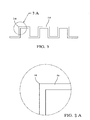
- the meaning of a sharp corner 24 is that the conductive line 20 turns abruptly through a predetermined angle (as shown in Figure 3 ).
- the conductive line 20 preferably has a castellated profile (comprising one or more square waves) as shown in Figures 1-3 .
- the conductive line 20 may have a zigzag profile (comprising one or more V- or W- shaped profiles). Further alternative profiles may be usable, as long as such profiles include at least one sharp corner.
- the conductive line 20 is a conducting metal strip, separated from the conducting ground plane 16, by a dielectric layer (the substrate 14).
- the substrate 14 may be any suitable material such as ceramic, FR4 (glass fibre reinforced epoxy resin, or PTFE, or may be a printed circuit board.
- One of the advantages of such a conductive line 20 is that it is easy to produce, has good reproducibility, and is cost effective.
- the specific profile of the conductive line 20 is important in the present invention.
- the sharp corners 24 serve as inhomogeneity for the electromagnetic waves.
- the ground plane 16 acts as a waveguide and the ground plane is separated from the conductive line 20 by the substrate 14.
- Figure 2 includes dimensions a and b which represent geometric lengths of the straight parts of the conductive line 20 (a is not necessarily equal to b); h is the height of the substrate 14; w is the width of the conductive line 20; and ⁇ r is the permittivity of the substrate 14. These dimensions/values are variables which are determined by simulation software to get an optimized result for a specific frequency range.
- the first and second circuit means 26, 32 each comprise a pair of diodes connected in parallel to one another which act to serve to shorten overvoltage (divert to ground) on the conductive line 20.
- diodes may be a "spark gap" which would be construed as apexes which are very close together (etched in the copper surface of the PCB). Only one spark gap would be necessary since the polarity would play no role. The high electric field strength would cause a spark which would also divert the voltage to ground. Further alternative arrangements include the use of other semiconductor devices.
- any electrostatic discharge creates a pulse which, because of its shortness, can be seen as a travelling wave, propagating from its point of entry (any point on the conductive line 20) to the input of the circuit 12.
- the pulse hits the non-linear conductive line 20, and the line acts as a form of RF (radiofrequency) network.
- the sharp corners 24 of the conductive line 20 cause a portion of the ESD pulse to be reflected back on itself.
- the pulse consists, mathematically, of a plurality of sinusoidal oscillations (such as Fourier). Any frequency component which is outside the bandwidth of the network is blocked. Therefore a portion of the potentially harmful ESD pulse is blocked. Further still, the diodes of the first circuit means 26 become conductive and neutralize another part of the ESD pulse.
- the diodes of the second circuit means 32 shorten another part of the pulse in the same manner.
- the diodes become conductive, there is a mismatch between conductive line 20 and the input to the circuit 12 which causes any remaining part of the ESD pulse is be reflected back.
- the diodes have a recovery time, the ESD pulse effectively sees a short circuit at the diode which reflects the pulse back in the other direction when the travelling time of the pulse is shorter than the recovery time of the diode. Finally, the pulse is damped to zero as reflection is repeated.
- the configuration (shape and size) of the conductive line 20 is determined to match the input impedance of the circuit 12 in any frequency range used by the circuit 12. Unlike prior art arrangements using discrete elements (resistors, capacitors, inductances), the conductive line 20 can be designed to have minimal affect on frequency response. The capacitance of the diodes does not influence the signal as the diodes can also be taken into consideration when determining the required configuration for the conductive line 20. Another advantage of the use of a conductive line 20 is that the line can be specifically designed for a broader frequency range, which is difficult to achieve when using single components. Test results shows that the protection device of the present invention can work effectively to 25 kV without influencing the behaviour of the protected circuit 12.
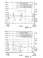
- Figure 5 shows the measurement of a scattering parameter s21 (s-parameters) with a conventional LC network but without a protective device in accordance with the present invention.
- the improvement provided by the present invention can be seen in Figure 4 .
- Both figures have the same sample marks 1-4 (5a, 6a). The higher the frequency, the bigger is the difference in insertion loss.
- Figure 4 shows the advantage of the present invention.
- the protection device of the present invention may be incorporated into an integrated circuit to protect the electronic circuit of the integrated circuit.
- the protection device may be connected to the input terminal of the electronic circuit, or to the output terminal of the electronic circuit, or a protection device may be connected to both the input and the output terminal.
- a single substrate may be used for both the protection device(s) and the electronic circuit.
- the present invention is particularly useful when used in a conjunction with an amplifier circuit connected to an antenna.
Landscapes
- Engineering & Computer Science (AREA)
- Microelectronics & Electronic Packaging (AREA)
- Physics & Mathematics (AREA)
- Electromagnetism (AREA)
- Semiconductor Integrated Circuits (AREA)
Abstract
a substrate (14) formed from dielectric material;
an electrically conductive ground plane (16) formed on one side of the substrate (14);
an electrically conductive line (20) formed on the other side of the substrate (14), the conductive line (20) having a non-linear profile and including one or more sharp corners;
a first circuit means (26) electrically connected to one end (28) of the conductive line (20) which is capable of diverting at least a portion of electrostatic discharge to electrical ground (16); and
a second circuit means (32) electrically connected to the other end (34) of the conductive line (20) which is capable of diverting at least a portion of electrostatic discharge to electrical ground (16).
Description
- The present invention relates to a protection device for protecting semiconductor devices or other electronic components and circuits against electrostatic discharge (ESD).
- Electronic integrated circuits, components, and other semiconductor devices generally operate at a voltage of 5 volts or less, and are therefore susceptible to damage by ESD. In particular, types of field effect transistors (FETs), especially those used for RF applications, can be damaged or destroyed by static voltages as low as 100 volts. RF components and circuits are susceptible to damage because of thin semiconductor layers, and the input stages of circuits which are capable of amplifying very small signals are especially sensitive to ESD. Known solutions to this problem include the integration of additional electronic devices (such as diodes) into a circuit for the sole purpose of protecting against ESD. These devices ground any voltage above a predetermined level in order to protect the circuit. A disadvantage of using these devices is their influence (due to capacitor effects) on the operation of the circuit itself. Another known solution is the use an LC network connected to the circuit input, and which acts as a filter to remove a portion of the pulse generated by ESD. A disadvantage of such LC networks is the negative effect these networks have on frequency response, which for certain circuits is unacceptable. In other words, the known protection devices can have a negative impact on the noise, frequency response and/or gain of the circuits these devices are meant to be protecting.
- The aim of the present invention is to provide a protection device for connection to an electronic component or circuit to protect such component or circuit against ESD, and which does not exhibit the negative effects of previously known devices.
- A protection device in accordance with the present invention is defined by the features specified in
claim 1. - The present invention also includes an integrated circuit comprising an electronic circuit with a protection device in accordance with the present invention connected thereto.
- The present invention overcomes the problems associated with the prior art in that the sharp corners of the conductive line cause a portion of the hazardous signal (ESD pulse) to be reflected back towards its source (for example, the antenna which may be the point of entrance for the ESD pulse/hazardous signal). The conductive line, along with the first and second circuit means, act as a filter to mitigate the effects of ESD, without having any substantive effect on the operation of the electronic circuit to which the protection device is connected.
- The present invention will now be described, by way of example, with reference to the accompanying drawings, in which:-
-
Figure 1 is a circuit diagram of a protection device in accordance with the present invention; -
Figure 2 is a perspective view of the conductive line and substrate of the protection device ofFigure 1 ; -
Figure 3 is an enlarged view of one of the sharp corners of the conductive line ofFigure 1 . -
Figure 4 is a graph illustrating insertion loss versus frequency when the protection circuit ofFigure 1 is used; and -
Figure 5 is a graph similar toFigure 4 illustrating insertion loss versus frequency when the protection circuit ofFigure 1 is not used. - Referring to
Figure 1-3 , aprotection device 10, in accordance with the present invention, for protecting an electronic component or circuit 12 (such as an amplifier circuit connected to an antenna) against electrostatic discharge, comprises asubstrate 14 formed from dielectric material; an electricallyconductive ground plane 16 formed on oneside 18 of the substrate; an electricallyconductive line 20 formed on theother side 22 of the substrate, the conductive line having a non-linear profile and including one or moresharp corners 24; a first circuit means 26 electrically connected to oneend 28 of the conductive line which is capable of diverting at least a portion of electrostatic discharge toelectrical ground 30; and a second circuit means 32 electrically connected to theother end 34 of the conductive line which is capable of diverting at least a portion of electrostatic discharge to electrical ground.Figure 1 also includes a capacitor C501 (which protects the input from DC signals), and resistors R202 and R203, which are not part of the protection circuit but are shown for reasons of completeness of an RF input circuitry. - For the sake of clarity in the present invention, the meaning of a non-linear profile is that the
conductive line 20 is not a straight line. Also, the meaning of asharp corner 24 is that theconductive line 20 turns abruptly through a predetermined angle (as shown inFigure 3 ). In this respect, theconductive line 20 preferably has a castellated profile (comprising one or more square waves) as shown inFigures 1-3 . As an alternative, theconductive line 20 may have a zigzag profile (comprising one or more V- or W- shaped profiles). Further alternative profiles may be usable, as long as such profiles include at least one sharp corner. - The
conductive line 20 is a conducting metal strip, separated from the conductingground plane 16, by a dielectric layer (the substrate 14). Thesubstrate 14 may be any suitable material such as ceramic, FR4 (glass fibre reinforced epoxy resin, or PTFE, or may be a printed circuit board. One of the advantages of such aconductive line 20 is that it is easy to produce, has good reproducibility, and is cost effective. The specific profile of theconductive line 20 is important in the present invention. Thesharp corners 24 serve as inhomogeneity for the electromagnetic waves. Theground plane 16 acts as a waveguide and the ground plane is separated from theconductive line 20 by thesubstrate 14. -
Figure 2 includes dimensions a and b which represent geometric lengths of the straight parts of the conductive line 20 (a is not necessarily equal to b); h is the height of thesubstrate 14; w is the width of theconductive line 20; and εr is the permittivity of thesubstrate 14. These dimensions/values are variables which are determined by simulation software to get an optimized result for a specific frequency range. - In the preferred embodiment shown in
Figures 1-3 , the first and second circuit means 26, 32 each comprise a pair of diodes connected in parallel to one another which act to serve to shorten overvoltage (divert to ground) on theconductive line 20. A possible alternative to diodes may be a "spark gap" which would be construed as apexes which are very close together (etched in the copper surface of the PCB). Only one spark gap would be necessary since the polarity would play no role. The high electric field strength would cause a spark which would also divert the voltage to ground. Further alternative arrangements include the use of other semiconductor devices. - Any electrostatic discharge creates a pulse which, because of its shortness, can be seen as a travelling wave, propagating from its point of entry (any point on the conductive line 20) to the input of the circuit 12. The pulse hits the non-linear
conductive line 20, and the line acts as a form of RF (radiofrequency) network. Thesharp corners 24 of theconductive line 20 cause a portion of the ESD pulse to be reflected back on itself. Additionally, the pulse consists, mathematically, of a plurality of sinusoidal oscillations (such as Fourier). Any frequency component which is outside the bandwidth of the network is blocked. Therefore a portion of the potentially harmful ESD pulse is blocked. Further still, the diodes of the first circuit means 26 become conductive and neutralize another part of the ESD pulse. Further still, the diodes of the second circuit means 32 shorten another part of the pulse in the same manner. When the diodes become conductive, there is a mismatch betweenconductive line 20 and the input to the circuit 12 which causes any remaining part of the ESD pulse is be reflected back. As the diodes have a recovery time, the ESD pulse effectively sees a short circuit at the diode which reflects the pulse back in the other direction when the travelling time of the pulse is shorter than the recovery time of the diode. Finally, the pulse is damped to zero as reflection is repeated. - The configuration (shape and size) of the
conductive line 20 is determined to match the input impedance of the circuit 12 in any frequency range used by the circuit 12. Unlike prior art arrangements using discrete elements (resistors, capacitors, inductances), theconductive line 20 can be designed to have minimal affect on frequency response. The capacitance of the diodes does not influence the signal as the diodes can also be taken into consideration when determining the required configuration for theconductive line 20. Another advantage of the use of aconductive line 20 is that the line can be specifically designed for a broader frequency range, which is difficult to achieve when using single components. Test results shows that the protection device of the present invention can work effectively to 25 kV without influencing the behaviour of the protected circuit 12. -
Figure 5 shows the measurement of a scattering parameter s21 (s-parameters) with a conventional LC network but without a protective device in accordance with the present invention. The improvement provided by the present invention can be seen inFigure 4 . Both figures have the same sample marks 1-4 (5a, 6a). The higher the frequency, the bigger is the difference in insertion loss.Figure 4 shows the advantage of the present invention. - The protection device of the present invention may be incorporated into an integrated circuit to protect the electronic circuit of the integrated circuit. The protection device may be connected to the input terminal of the electronic circuit, or to the output terminal of the electronic circuit, or a protection device may be connected to both the input and the output terminal. In this arrangement, a single substrate may be used for both the protection device(s) and the electronic circuit.
- The present invention is particularly useful when used in a conjunction with an amplifier circuit connected to an antenna.
Claims (8)
- A protection device for protecting an electronic component or circuit against electrostatic discharge, the protection device comprising
a substrate formed from dielectric material;
an electrically conductive ground plane formed on one side of the sub strate;
an electrically conductive line formed on the other side of the substrate, the conductive line having a non-linear profile and including one or more sharp corners;
a first circuit means electrically connected to one end of the conductive line which is capable of diverting at least a portion of electrostatic discharge to electrical ground; and
a second circuit means electrically connected to the other end of the conductive line which is capable of diverting at least a portion of electrostatic discharge to electrical ground. - A protection device as claimed in claim 1, wherein the first and second circuit means are substantially identical.
- A protection device as claimed in claim 1 or claim 2, wherein the first and second circuit means each comprise first and second diodes electrically connected in parallel between the conductive line and electrical ground.
- A protection device as claimed in any one of claims 1 to 3, wherein the conductive line has a castellated profile.
- A protection device as claimed in any one of claims 1 to 3, wherein the conductive line has a zigzag profile.
- A protection device as claimed in any one of claims 1 to 5, wherein the conductive line has been formed by etching or milling an electrically conductive layer formed on the substrate.
- An integrated circuit comprising an electronic circuit having an input terminal and an output terminal; and a protection device as claimed in any one of claims 1 to 6, wherein one of the ends of the conductive line is electrically connected to the input terminal or the output terminal.
- An integrated circuit as claimed in claim 7, wherein a first protection device as claimed in any one of claims 1 to 6 is electrically connected to the input terminal, and a second protection device as claimed in any one of claims 1 to 6 is electrically connected to the output terminal.
Priority Applications (1)
| Application Number | Priority Date | Filing Date | Title |
|---|---|---|---|
| EP11173581.7A EP2547181B1 (en) | 2011-07-12 | 2011-07-12 | A protection device for ESD protection |
Applications Claiming Priority (1)
| Application Number | Priority Date | Filing Date | Title |
|---|---|---|---|
| EP11173581.7A EP2547181B1 (en) | 2011-07-12 | 2011-07-12 | A protection device for ESD protection |
Publications (2)
| Publication Number | Publication Date |
|---|---|
| EP2547181A1 true EP2547181A1 (en) | 2013-01-16 |
| EP2547181B1 EP2547181B1 (en) | 2017-03-29 |
Family
ID=44582198
Family Applications (1)
| Application Number | Title | Priority Date | Filing Date |
|---|---|---|---|
| EP11173581.7A Not-in-force EP2547181B1 (en) | 2011-07-12 | 2011-07-12 | A protection device for ESD protection |
Country Status (1)
| Country | Link |
|---|---|
| EP (1) | EP2547181B1 (en) |
Citations (3)
| Publication number | Priority date | Publication date | Assignee | Title |
|---|---|---|---|---|
| US20060066417A1 (en) * | 2004-09-30 | 2006-03-30 | Murata Manufacturing Co., Ltd. | Wiring pattern structure of differential transmission paths |
| US20090021873A1 (en) * | 2006-02-17 | 2009-01-22 | Nxp B.V. | Electro static discharge protection in integrated circuits |
| US20100277840A1 (en) * | 2009-05-04 | 2010-11-04 | Bo-Jr Huang | V-Band Radio Frequency Electrostatic Discharge Protection Circuit |
-
2011
- 2011-07-12 EP EP11173581.7A patent/EP2547181B1/en not_active Not-in-force
Patent Citations (3)
| Publication number | Priority date | Publication date | Assignee | Title |
|---|---|---|---|---|
| US20060066417A1 (en) * | 2004-09-30 | 2006-03-30 | Murata Manufacturing Co., Ltd. | Wiring pattern structure of differential transmission paths |
| US20090021873A1 (en) * | 2006-02-17 | 2009-01-22 | Nxp B.V. | Electro static discharge protection in integrated circuits |
| US20100277840A1 (en) * | 2009-05-04 | 2010-11-04 | Bo-Jr Huang | V-Band Radio Frequency Electrostatic Discharge Protection Circuit |
Also Published As
| Publication number | Publication date |
|---|---|
| EP2547181B1 (en) | 2017-03-29 |
Similar Documents
| Publication | Publication Date | Title |
|---|---|---|
| US6115227A (en) | Surge suppressor device | |
| US7821759B2 (en) | Surge absorption circuit | |
| US8994471B2 (en) | Stacked diode limiter | |
| KR101012965B1 (en) | Composite device | |
| TWI608651B (en) | One quarter wavelength transmission line based electrostatic discharge (esd) protection for integrated circuits | |
| Mias | Waveguide and free-space demonstration of tunable frequency selective surface | |
| JP4483552B2 (en) | Surge absorption circuit | |
| EP2547181B1 (en) | A protection device for ESD protection | |
| US20060291128A1 (en) | Surge absorption circuit | |
| Chernikova et al. | Comparative analysis of an LC-filter and a reflection symmetric modal filter | |
| JP4449838B2 (en) | Surge absorption circuit | |
| US20200020651A1 (en) | Radio-frequency module | |
| US6999294B2 (en) | Waveguide | |
| CN115299184A (en) | Circuit board and electronic device | |
| RU2748423C1 (en) | Strip structure protecting against extra short pulses in differential and synphase modes | |
| US10083826B2 (en) | Input protection circuit for high-speed analogue signal and time-of-flight mass spectrometer | |
| JP3959091B2 (en) | Surge absorption circuit | |
| US7881065B1 (en) | Circuit with improved electrostatic discharge susceptibility | |
| RU2860295C1 (en) | 8-conductor strip structure protecting against ultra-short pulses in common-mode and differential modes | |
| CN111315115A (en) | Implementation method for preventing secondary electrostatic discharge, circuit board and equipment | |
| Murmansky et al. | Investigating the Effect of Ground Distance on the Characteristics of a Coupled Meander Microstrip Line | |
| Sasaki et al. | A new decoupling circuit for suppressing radiated emissions due to power plane resonance | |
| US20240333245A1 (en) | Filter device | |
| Mousavi et al. | IC-based Antenna Switch Modeling and Robustness Evaluation for SEED Applications | |
| KR200273943Y1 (en) | An attenuator having the means of lightning arrester |
Legal Events
| Date | Code | Title | Description |
|---|---|---|---|
| PUAI | Public reference made under article 153(3) epc to a published international application that has entered the european phase |
Free format text: ORIGINAL CODE: 0009012 |
|
| AK | Designated contracting states |
Kind code of ref document: A1 Designated state(s): AL AT BE BG CH CY CZ DE DK EE ES FI FR GB GR HR HU IE IS IT LI LT LU LV MC MK MT NL NO PL PT RO RS SE SI SK SM TR |
|
| AX | Request for extension of the european patent |
Extension state: BA ME |
|
| 17P | Request for examination filed |
Effective date: 20130716 |
|
| RBV | Designated contracting states (corrected) |
Designated state(s): AL AT BE BG CH CY CZ DE DK EE ES FI FR GB GR HR HU IE IS IT LI LT LU LV MC MK MT NL NO PL PT RO RS SE SI SK SM TR |
|
| 17Q | First examination report despatched |
Effective date: 20130902 |
|
| GRAP | Despatch of communication of intention to grant a patent |
Free format text: ORIGINAL CODE: EPIDOSNIGR1 |
|
| RIC1 | Information provided on ipc code assigned before grant |
Ipc: H05K 1/02 20060101AFI20161024BHEP Ipc: H03K 17/0812 20060101ALN20161024BHEP Ipc: H03K 17/0814 20060101ALN20161024BHEP Ipc: H05K 9/00 20060101ALI20161024BHEP |
|
| INTG | Intention to grant announced |
Effective date: 20161201 |
|
| GRAS | Grant fee paid |
Free format text: ORIGINAL CODE: EPIDOSNIGR3 |
|
| GRAA | (expected) grant |
Free format text: ORIGINAL CODE: 0009210 |
|
| AK | Designated contracting states |
Kind code of ref document: B1 Designated state(s): AL AT BE BG CH CY CZ DE DK EE ES FI FR GB GR HR HU IE IS IT LI LT LU LV MC MK MT NL NO PL PT RO RS SE SI SK SM TR |
|
| REG | Reference to a national code |
Ref country code: GB Ref legal event code: FG4D |
|
| REG | Reference to a national code |
Ref country code: CH Ref legal event code: EP |
|
| REG | Reference to a national code |
Ref country code: AT Ref legal event code: REF Ref document number: 880856 Country of ref document: AT Kind code of ref document: T Effective date: 20170415 |
|
| REG | Reference to a national code |
Ref country code: IE Ref legal event code: FG4D |
|
| REG | Reference to a national code |
Ref country code: DE Ref legal event code: R096 Ref document number: 602011036388 Country of ref document: DE |
|
| REG | Reference to a national code |
Ref country code: FR Ref legal event code: PLFP Year of fee payment: 7 |
|
| PG25 | Lapsed in a contracting state [announced via postgrant information from national office to epo] |
Ref country code: NO Free format text: LAPSE BECAUSE OF FAILURE TO SUBMIT A TRANSLATION OF THE DESCRIPTION OR TO PAY THE FEE WITHIN THE PRESCRIBED TIME-LIMIT Effective date: 20170629 Ref country code: GR Free format text: LAPSE BECAUSE OF FAILURE TO SUBMIT A TRANSLATION OF THE DESCRIPTION OR TO PAY THE FEE WITHIN THE PRESCRIBED TIME-LIMIT Effective date: 20170630 Ref country code: FI Free format text: LAPSE BECAUSE OF FAILURE TO SUBMIT A TRANSLATION OF THE DESCRIPTION OR TO PAY THE FEE WITHIN THE PRESCRIBED TIME-LIMIT Effective date: 20170329 Ref country code: HR Free format text: LAPSE BECAUSE OF FAILURE TO SUBMIT A TRANSLATION OF THE DESCRIPTION OR TO PAY THE FEE WITHIN THE PRESCRIBED TIME-LIMIT Effective date: 20170329 Ref country code: LT Free format text: LAPSE BECAUSE OF FAILURE TO SUBMIT A TRANSLATION OF THE DESCRIPTION OR TO PAY THE FEE WITHIN THE PRESCRIBED TIME-LIMIT Effective date: 20170329 |
|
| REG | Reference to a national code |
Ref country code: NL Ref legal event code: MP Effective date: 20170329 |
|
| REG | Reference to a national code |
Ref country code: AT Ref legal event code: MK05 Ref document number: 880856 Country of ref document: AT Kind code of ref document: T Effective date: 20170329 |
|
| PG25 | Lapsed in a contracting state [announced via postgrant information from national office to epo] |
Ref country code: BG Free format text: LAPSE BECAUSE OF FAILURE TO SUBMIT A TRANSLATION OF THE DESCRIPTION OR TO PAY THE FEE WITHIN THE PRESCRIBED TIME-LIMIT Effective date: 20170629 Ref country code: SE Free format text: LAPSE BECAUSE OF FAILURE TO SUBMIT A TRANSLATION OF THE DESCRIPTION OR TO PAY THE FEE WITHIN THE PRESCRIBED TIME-LIMIT Effective date: 20170329 Ref country code: RS Free format text: LAPSE BECAUSE OF FAILURE TO SUBMIT A TRANSLATION OF THE DESCRIPTION OR TO PAY THE FEE WITHIN THE PRESCRIBED TIME-LIMIT Effective date: 20170329 Ref country code: LV Free format text: LAPSE BECAUSE OF FAILURE TO SUBMIT A TRANSLATION OF THE DESCRIPTION OR TO PAY THE FEE WITHIN THE PRESCRIBED TIME-LIMIT Effective date: 20170329 |
|
| PG25 | Lapsed in a contracting state [announced via postgrant information from national office to epo] |
Ref country code: NL Free format text: LAPSE BECAUSE OF FAILURE TO SUBMIT A TRANSLATION OF THE DESCRIPTION OR TO PAY THE FEE WITHIN THE PRESCRIBED TIME-LIMIT Effective date: 20170329 |
|
| PG25 | Lapsed in a contracting state [announced via postgrant information from national office to epo] |
Ref country code: SK Free format text: LAPSE BECAUSE OF FAILURE TO SUBMIT A TRANSLATION OF THE DESCRIPTION OR TO PAY THE FEE WITHIN THE PRESCRIBED TIME-LIMIT Effective date: 20170329 Ref country code: ES Free format text: LAPSE BECAUSE OF FAILURE TO SUBMIT A TRANSLATION OF THE DESCRIPTION OR TO PAY THE FEE WITHIN THE PRESCRIBED TIME-LIMIT Effective date: 20170329 Ref country code: EE Free format text: LAPSE BECAUSE OF FAILURE TO SUBMIT A TRANSLATION OF THE DESCRIPTION OR TO PAY THE FEE WITHIN THE PRESCRIBED TIME-LIMIT Effective date: 20170329 Ref country code: RO Free format text: LAPSE BECAUSE OF FAILURE TO SUBMIT A TRANSLATION OF THE DESCRIPTION OR TO PAY THE FEE WITHIN THE PRESCRIBED TIME-LIMIT Effective date: 20170329 Ref country code: AT Free format text: LAPSE BECAUSE OF FAILURE TO SUBMIT A TRANSLATION OF THE DESCRIPTION OR TO PAY THE FEE WITHIN THE PRESCRIBED TIME-LIMIT Effective date: 20170329 Ref country code: CZ Free format text: LAPSE BECAUSE OF FAILURE TO SUBMIT A TRANSLATION OF THE DESCRIPTION OR TO PAY THE FEE WITHIN THE PRESCRIBED TIME-LIMIT Effective date: 20170329 |
|
| PGFP | Annual fee paid to national office [announced via postgrant information from national office to epo] |
Ref country code: FR Payment date: 20170724 Year of fee payment: 7 |
|
| PG25 | Lapsed in a contracting state [announced via postgrant information from national office to epo] |
Ref country code: PT Free format text: LAPSE BECAUSE OF FAILURE TO SUBMIT A TRANSLATION OF THE DESCRIPTION OR TO PAY THE FEE WITHIN THE PRESCRIBED TIME-LIMIT Effective date: 20170731 Ref country code: PL Free format text: LAPSE BECAUSE OF FAILURE TO SUBMIT A TRANSLATION OF THE DESCRIPTION OR TO PAY THE FEE WITHIN THE PRESCRIBED TIME-LIMIT Effective date: 20170329 Ref country code: IS Free format text: LAPSE BECAUSE OF FAILURE TO SUBMIT A TRANSLATION OF THE DESCRIPTION OR TO PAY THE FEE WITHIN THE PRESCRIBED TIME-LIMIT Effective date: 20170729 Ref country code: SM Free format text: LAPSE BECAUSE OF FAILURE TO SUBMIT A TRANSLATION OF THE DESCRIPTION OR TO PAY THE FEE WITHIN THE PRESCRIBED TIME-LIMIT Effective date: 20170329 |
|
| REG | Reference to a national code |
Ref country code: DE Ref legal event code: R097 Ref document number: 602011036388 Country of ref document: DE |
|
| PG25 | Lapsed in a contracting state [announced via postgrant information from national office to epo] |
Ref country code: DK Free format text: LAPSE BECAUSE OF FAILURE TO SUBMIT A TRANSLATION OF THE DESCRIPTION OR TO PAY THE FEE WITHIN THE PRESCRIBED TIME-LIMIT Effective date: 20170329 |
|
| REG | Reference to a national code |
Ref country code: DE Ref legal event code: R084 Ref document number: 602011036388 Country of ref document: DE |
|
| PLBE | No opposition filed within time limit |
Free format text: ORIGINAL CODE: 0009261 |
|
| STAA | Information on the status of an ep patent application or granted ep patent |
Free format text: STATUS: NO OPPOSITION FILED WITHIN TIME LIMIT |
|
| REG | Reference to a national code |
Ref country code: GB Ref legal event code: 746 Effective date: 20180202 Ref country code: CH Ref legal event code: PL |
|
| 26N | No opposition filed |
Effective date: 20180103 |
|
| REG | Reference to a national code |
Ref country code: IE Ref legal event code: MM4A |
|
| PG25 | Lapsed in a contracting state [announced via postgrant information from national office to epo] |
Ref country code: LI Free format text: LAPSE BECAUSE OF NON-PAYMENT OF DUE FEES Effective date: 20170731 Ref country code: CH Free format text: LAPSE BECAUSE OF NON-PAYMENT OF DUE FEES Effective date: 20170731 Ref country code: IE Free format text: LAPSE BECAUSE OF NON-PAYMENT OF DUE FEES Effective date: 20170712 |
|
| PG25 | Lapsed in a contracting state [announced via postgrant information from national office to epo] |
Ref country code: SI Free format text: LAPSE BECAUSE OF FAILURE TO SUBMIT A TRANSLATION OF THE DESCRIPTION OR TO PAY THE FEE WITHIN THE PRESCRIBED TIME-LIMIT Effective date: 20170329 |
|
| REG | Reference to a national code |
Ref country code: BE Ref legal event code: MM Effective date: 20170731 |
|
| PG25 | Lapsed in a contracting state [announced via postgrant information from national office to epo] |
Ref country code: LU Free format text: LAPSE BECAUSE OF NON-PAYMENT OF DUE FEES Effective date: 20170712 |
|
| PG25 | Lapsed in a contracting state [announced via postgrant information from national office to epo] |
Ref country code: BE Free format text: LAPSE BECAUSE OF NON-PAYMENT OF DUE FEES Effective date: 20170731 |
|
| PG25 | Lapsed in a contracting state [announced via postgrant information from national office to epo] |
Ref country code: MT Free format text: LAPSE BECAUSE OF NON-PAYMENT OF DUE FEES Effective date: 20170712 |
|
| PGFP | Annual fee paid to national office [announced via postgrant information from national office to epo] |
Ref country code: IT Payment date: 20180724 Year of fee payment: 8 |
|
| PG25 | Lapsed in a contracting state [announced via postgrant information from national office to epo] |
Ref country code: FR Free format text: LAPSE BECAUSE OF NON-PAYMENT OF DUE FEES Effective date: 20180731 |
|
| PG25 | Lapsed in a contracting state [announced via postgrant information from national office to epo] |
Ref country code: HU Free format text: LAPSE BECAUSE OF FAILURE TO SUBMIT A TRANSLATION OF THE DESCRIPTION OR TO PAY THE FEE WITHIN THE PRESCRIBED TIME-LIMIT; INVALID AB INITIO Effective date: 20110712 Ref country code: MC Free format text: LAPSE BECAUSE OF FAILURE TO SUBMIT A TRANSLATION OF THE DESCRIPTION OR TO PAY THE FEE WITHIN THE PRESCRIBED TIME-LIMIT Effective date: 20170329 |
|
| PG25 | Lapsed in a contracting state [announced via postgrant information from national office to epo] |
Ref country code: CY Free format text: LAPSE BECAUSE OF NON-PAYMENT OF DUE FEES Effective date: 20170329 |
|
| PG25 | Lapsed in a contracting state [announced via postgrant information from national office to epo] |
Ref country code: MK Free format text: LAPSE BECAUSE OF FAILURE TO SUBMIT A TRANSLATION OF THE DESCRIPTION OR TO PAY THE FEE WITHIN THE PRESCRIBED TIME-LIMIT Effective date: 20170329 |
|
| PGFP | Annual fee paid to national office [announced via postgrant information from national office to epo] |
Ref country code: DE Payment date: 20190927 Year of fee payment: 9 |
|
| PG25 | Lapsed in a contracting state [announced via postgrant information from national office to epo] |
Ref country code: TR Free format text: LAPSE BECAUSE OF FAILURE TO SUBMIT A TRANSLATION OF THE DESCRIPTION OR TO PAY THE FEE WITHIN THE PRESCRIBED TIME-LIMIT Effective date: 20170329 |
|
| PG25 | Lapsed in a contracting state [announced via postgrant information from national office to epo] |
Ref country code: AL Free format text: LAPSE BECAUSE OF FAILURE TO SUBMIT A TRANSLATION OF THE DESCRIPTION OR TO PAY THE FEE WITHIN THE PRESCRIBED TIME-LIMIT Effective date: 20170329 |
|
| PG25 | Lapsed in a contracting state [announced via postgrant information from national office to epo] |
Ref country code: IT Free format text: LAPSE BECAUSE OF NON-PAYMENT OF DUE FEES Effective date: 20190712 |
|
| PGFP | Annual fee paid to national office [announced via postgrant information from national office to epo] |
Ref country code: GB Payment date: 20200727 Year of fee payment: 10 |
|
| REG | Reference to a national code |
Ref country code: DE Ref legal event code: R119 Ref document number: 602011036388 Country of ref document: DE |
|
| PG25 | Lapsed in a contracting state [announced via postgrant information from national office to epo] |
Ref country code: DE Free format text: LAPSE BECAUSE OF NON-PAYMENT OF DUE FEES Effective date: 20210202 |
|
| GBPC | Gb: european patent ceased through non-payment of renewal fee |
Effective date: 20210712 |
|
| PG25 | Lapsed in a contracting state [announced via postgrant information from national office to epo] |
Ref country code: GB Free format text: LAPSE BECAUSE OF NON-PAYMENT OF DUE FEES Effective date: 20210712 |