EP2546987A2 - Nested Composite Switch - Google Patents
Nested Composite Switch Download PDFInfo
- Publication number
- EP2546987A2 EP2546987A2 EP12175467A EP12175467A EP2546987A2 EP 2546987 A2 EP2546987 A2 EP 2546987A2 EP 12175467 A EP12175467 A EP 12175467A EP 12175467 A EP12175467 A EP 12175467A EP 2546987 A2 EP2546987 A2 EP 2546987A2
- Authority
- EP
- European Patent Office
- Prior art keywords
- transistor
- composite switch
- nested
- composite
- normally
- Prior art date
- Legal status (The legal status is an assumption and is not a legal conclusion. Google has not performed a legal analysis and makes no representation as to the accuracy of the status listed.)
- Withdrawn
Links
- 239000002131 composite material Substances 0.000 title claims abstract description 179
- 230000015556 catabolic process Effects 0.000 claims abstract description 22
- 230000005669 field effect Effects 0.000 claims description 5
- 239000004065 semiconductor Substances 0.000 description 12
- 239000000463 material Substances 0.000 description 10
- XUIMIQQOPSSXEZ-UHFFFAOYSA-N Silicon Chemical compound [Si] XUIMIQQOPSSXEZ-UHFFFAOYSA-N 0.000 description 9
- 229910052710 silicon Inorganic materials 0.000 description 9
- 239000010703 silicon Substances 0.000 description 9
- 229910002601 GaN Inorganic materials 0.000 description 7
- JMASRVWKEDWRBT-UHFFFAOYSA-N Gallium nitride Chemical compound [Ga]#N JMASRVWKEDWRBT-UHFFFAOYSA-N 0.000 description 6
- 150000001875 compounds Chemical class 0.000 description 4
- 238000010586 diagram Methods 0.000 description 4
- 229910045601 alloy Inorganic materials 0.000 description 3
- 239000000956 alloy Substances 0.000 description 3
- AJGDITRVXRPLBY-UHFFFAOYSA-N aluminum indium Chemical compound [Al].[In] AJGDITRVXRPLBY-UHFFFAOYSA-N 0.000 description 3
- 229910052738 indium Inorganic materials 0.000 description 3
- APFVFJFRJDLVQX-UHFFFAOYSA-N indium atom Chemical compound [In] APFVFJFRJDLVQX-UHFFFAOYSA-N 0.000 description 3
- 239000000758 substrate Substances 0.000 description 3
- IJGRMHOSHXDMSA-UHFFFAOYSA-N Atomic nitrogen Chemical compound N#N IJGRMHOSHXDMSA-UHFFFAOYSA-N 0.000 description 2
- 229910000577 Silicon-germanium Inorganic materials 0.000 description 2
- RNQKDQAVIXDKAG-UHFFFAOYSA-N aluminum gallium Chemical compound [Al].[Ga] RNQKDQAVIXDKAG-UHFFFAOYSA-N 0.000 description 2
- 230000008901 benefit Effects 0.000 description 2
- 239000013078 crystal Substances 0.000 description 2
- 229910021480 group 4 element Inorganic materials 0.000 description 2
- 238000000034 method Methods 0.000 description 2
- 150000004767 nitrides Chemical class 0.000 description 2
- 230000003071 parasitic effect Effects 0.000 description 2
- JBRZTFJDHDCESZ-UHFFFAOYSA-N AsGa Chemical compound [As]#[Ga] JBRZTFJDHDCESZ-UHFFFAOYSA-N 0.000 description 1
- ZOXJGFHDIHLPTG-UHFFFAOYSA-N Boron Chemical compound [B] ZOXJGFHDIHLPTG-UHFFFAOYSA-N 0.000 description 1
- OKTJSMMVPCPJKN-UHFFFAOYSA-N Carbon Chemical compound [C] OKTJSMMVPCPJKN-UHFFFAOYSA-N 0.000 description 1
- GYHNNYVSQQEPJS-UHFFFAOYSA-N Gallium Chemical compound [Ga] GYHNNYVSQQEPJS-UHFFFAOYSA-N 0.000 description 1
- 229910001218 Gallium arsenide Inorganic materials 0.000 description 1
- 229910000530 Gallium indium arsenide Inorganic materials 0.000 description 1
- 229910052782 aluminium Inorganic materials 0.000 description 1
- XAGFODPZIPBFFR-UHFFFAOYSA-N aluminium Chemical compound [Al] XAGFODPZIPBFFR-UHFFFAOYSA-N 0.000 description 1
- QVGXLLKOCUKJST-UHFFFAOYSA-N atomic oxygen Chemical compound [O] QVGXLLKOCUKJST-UHFFFAOYSA-N 0.000 description 1
- 229910052796 boron Inorganic materials 0.000 description 1
- 229910052799 carbon Inorganic materials 0.000 description 1
- 230000008878 coupling Effects 0.000 description 1
- 238000010168 coupling process Methods 0.000 description 1
- 238000005859 coupling reaction Methods 0.000 description 1
- 230000000694 effects Effects 0.000 description 1
- 229910052733 gallium Inorganic materials 0.000 description 1
- 229910052732 germanium Inorganic materials 0.000 description 1
- GNPVGFCGXDBREM-UHFFFAOYSA-N germanium atom Chemical compound [Ge] GNPVGFCGXDBREM-UHFFFAOYSA-N 0.000 description 1
- 229910021478 group 5 element Inorganic materials 0.000 description 1
- 238000002513 implantation Methods 0.000 description 1
- 230000010354 integration Effects 0.000 description 1
- 238000004519 manufacturing process Methods 0.000 description 1
- 238000004377 microelectronic Methods 0.000 description 1
- 238000012986 modification Methods 0.000 description 1
- 230000004048 modification Effects 0.000 description 1
- 229910003465 moissanite Inorganic materials 0.000 description 1
- 229910052757 nitrogen Inorganic materials 0.000 description 1
- 239000001301 oxygen Substances 0.000 description 1
- 229910052760 oxygen Inorganic materials 0.000 description 1
- 230000010287 polarization Effects 0.000 description 1
- 230000008569 process Effects 0.000 description 1
- 230000008707 rearrangement Effects 0.000 description 1
- 229910052594 sapphire Inorganic materials 0.000 description 1
- 239000010980 sapphire Substances 0.000 description 1
- 238000000926 separation method Methods 0.000 description 1
- 229910010271 silicon carbide Inorganic materials 0.000 description 1
- 238000006467 substitution reaction Methods 0.000 description 1
- WGPCGCOKHWGKJJ-UHFFFAOYSA-N sulfanylidenezinc Chemical compound [Zn]=S WGPCGCOKHWGKJJ-UHFFFAOYSA-N 0.000 description 1
- 230000005533 two-dimensional electron gas Effects 0.000 description 1
- 229910052984 zinc sulfide Inorganic materials 0.000 description 1
Images

Classifications
-
- H—ELECTRICITY
- H03—ELECTRONIC CIRCUITRY
- H03K—PULSE TECHNIQUE
- H03K17/00—Electronic switching or gating, i.e. not by contact-making and –breaking
- H03K17/51—Electronic switching or gating, i.e. not by contact-making and –breaking characterised by the components used
- H03K17/56—Electronic switching or gating, i.e. not by contact-making and –breaking characterised by the components used by the use, as active elements, of semiconductor devices
- H03K17/567—Circuits characterised by the use of more than one type of semiconductor device, e.g. BIMOS, composite devices such as IGBT
-
- H—ELECTRICITY
- H03—ELECTRONIC CIRCUITRY
- H03K—PULSE TECHNIQUE
- H03K17/00—Electronic switching or gating, i.e. not by contact-making and –breaking
- H03K17/10—Modifications for increasing the maximum permissible switched voltage
- H03K17/107—Modifications for increasing the maximum permissible switched voltage in composite switches
-
- H—ELECTRICITY
- H03—ELECTRONIC CIRCUITRY
- H03K—PULSE TECHNIQUE
- H03K17/00—Electronic switching or gating, i.e. not by contact-making and –breaking
- H03K17/16—Modifications for eliminating interference voltages or currents
- H03K17/168—Modifications for eliminating interference voltages or currents in composite switches
-
- H—ELECTRICITY
- H03—ELECTRONIC CIRCUITRY
- H03K—PULSE TECHNIQUE
- H03K17/00—Electronic switching or gating, i.e. not by contact-making and –breaking
- H03K17/30—Modifications for providing a predetermined threshold before switching
- H03K17/302—Modifications for providing a predetermined threshold before switching in field-effect transistor switches
-
- H—ELECTRICITY
- H10—SEMICONDUCTOR DEVICES; ELECTRIC SOLID-STATE DEVICES NOT OTHERWISE PROVIDED FOR
- H10D—INORGANIC ELECTRIC SEMICONDUCTOR DEVICES
- H10D84/00—Integrated devices formed in or on semiconductor substrates that comprise only semiconducting layers, e.g. on Si wafers or on GaAs-on-Si wafers
- H10D84/01—Manufacture or treatment
- H10D84/02—Manufacture or treatment characterised by using material-based technologies
- H10D84/08—Manufacture or treatment characterised by using material-based technologies using combinations of technologies, e.g. using both Si and SiC technologies or using both Si and Group III-V technologies
-
- H—ELECTRICITY
- H10—SEMICONDUCTOR DEVICES; ELECTRIC SOLID-STATE DEVICES NOT OTHERWISE PROVIDED FOR
- H10D—INORGANIC ELECTRIC SEMICONDUCTOR DEVICES
- H10D84/00—Integrated devices formed in or on semiconductor substrates that comprise only semiconducting layers, e.g. on Si wafers or on GaAs-on-Si wafers
- H10D84/01—Manufacture or treatment
-
- H—ELECTRICITY
- H10—SEMICONDUCTOR DEVICES; ELECTRIC SOLID-STATE DEVICES NOT OTHERWISE PROVIDED FOR
- H10D—INORGANIC ELECTRIC SEMICONDUCTOR DEVICES
- H10D84/00—Integrated devices formed in or on semiconductor substrates that comprise only semiconducting layers, e.g. on Si wafers or on GaAs-on-Si wafers
- H10D84/80—Integrated devices formed in or on semiconductor substrates that comprise only semiconducting layers, e.g. on Si wafers or on GaAs-on-Si wafers characterised by the integration of at least one component covered by groups H10D12/00 or H10D30/00, e.g. integration of IGFETs
- H10D84/811—Combinations of field-effect devices and one or more diodes, capacitors or resistors
Definitions
- group III-V refers to a compound semiconductor that includes a group V element and at least one group III element.
- III-Nitride or III-N refers to a compound semiconductor that includes nitrogen (N) and at least one group III element including aluminum (Al), gallium (Ga), indium (In), and boron (B), and including but not limited to any of its alloys, such as aluminum gallium nitride (Al x Ga (1-x) N), indium gallium nitride (In y Ga (1-y) N), aluminum indium gallium nitride (Al x In y Ga (1-x-y) N), gallium arsenide phosphide nitride (GaAs a P b N (1-a-b) ), and aluminum indium gallium arsenide phosphide nitride (Al x In y Ga (1-x-y) As a P b N (1
- III-Nitride also refers generally to any polarity including but not limited to Ga-polar, N-polar, semi-polar or non-polar crystal orientations.
- a III-Nitride material may also include either the Wurtzitic, Zincblende or mixed polytypes, and may include single-crystal, monocrystalline, polycrystalline, or amorphous structures.
- group IV refers to a semiconductor that includes at least one group four element including silicon (Si), germanium (Ge), and carbon (C), and also includes compound semiconductors such as SiGe and SiC, for example.
- Group IV may also refer to a semiconductor material which consists of layers of group IV elements or doping of group IV elements to produce strained silicon or other strained group IV material.
- group IV based composite substrates may include silicon on insulstor (SOI), separation by implantation of oxygen (SIMOX) process substrates, and silicon on sapphire (SOS), for example.
- SOI silicon on insulstor
- SIMOX separation by implantation of oxygen
- SOS silicon on sapphire
- a group IV device may include devices formed using standard CMOS processing, but may also include NMOS and PMOS device processing.
- the terms “LV device,” “low voltage semiconductor device,” “low voltage transistor, low voltage switch” and the like refer to a low voltage device, with a typical breakdown voltage rating less than an “intermediate device,” as described below.
- the LV device can include any suitable semiconductor material that forms a field-effect transistor (FET) such as an insulated-gate FET (IGFET), for example.
- FET field-effect transistor
- Suitable semiconductor materials include group IV semiconductor materials such as Si, strained silicon, SiGe, SiC, and group III-V materials including III-As, III-P, III-Nitride or any of their alloys.
- intermediate device refers to a device with a typical breakdown voltage greater than the LV device and less than a "primary device”.
- primary device, primary transistor or primary switch refers to a device with a typical breakdown voltage greater than both the intermediate device and the LV device.
- group III-V field-effect transistors FETs
- HEMTs high mobility electron transistors
- III-Nitride FETs and III-Nitride HEMTs are often desirable for their high efficiency and high-voltage operation.
- group III-V transistors with other FETs, such as group IV FETs, to create high performance composite switches.
- a depletion mode (normally ON) III-Nitride or other group III-V transistor can be cascoded with an enhancement mode (normally OFF) low-voltage (LV) group IV transistor, for example a silicon FET, to produce an enhancement mode (normally OFF) composite power switch.
- an enhancement mode normally OFF
- LV group IV transistor for example a silicon FET
- the performance of the composite switch can be limited by the on-state and voltage breakdown characteristics of the LV group IV transistor used.
- the breakdown voltage for a given on-state resistance of the LV group IV transistor may be insufficient to support the required pinch-off voltage required to maintain the group III-V transistor in a satisfactorily OFF condition.
- the present disclosure is directed to a nested composite switch, substantially as shown in and/or described in connection with at least one of the figures, and as set forth more completely in the claims.
- Group III-V semiconductors include III-Nitride materials formed of gallium nitride (GaN) and/or its alloys, such as aluminum gallium nitride (AlGaN), indium gallium nitride (InGaN), and aluminum indium gallium nitride (AlInGaN). These materials are semiconductor compounds that have a relatively wide, direct bandgap and strong piezoelectric polarizations, and can support high breakdown fields, high saturation velocities, and the creation of two-dimensional electron gases (2DEGs). As a result, III-Nitride materials such as GaN are used in many microelectronic applications such as depletion mode (e.g., normally ON) power field-effect transistors (FETs) and high electron mobility transistors (HEMTs).
- depletion mode e.g., normally ON
- FETs field-effect transistors
- HEMTs high electron mobility transistors
- a depletion mode (normally ON) III-Nitride or other group III-V transistor can be cascoded with an enhancement mode (normally OFF) low voltage (LV) transistor, such as a silicon or other LV group IV transistor, to produce an enhancement mode composite power switch.
- LV low voltage
- the performance of the composite switch can be limited by the on-state and voltage breakdown characteristics of the LV group IV transistor used.
- the breakdown voltage for a given on-state resistance of the LV group IV transistor may be insufficient to support the required pinch-off voltage required to maintain the group III-V transistor in a satisfactorily OFF condition.
- an intermediate III-V transistor may be used in a nested cascode configuration.
- the present application is directed to a nested composite switch capable of providing enhanced voltage breakdown resistance while providing advantages such as fast switching speed, high transconductance, low switching charge, low threshold voltage, and low on-state resistance typically associated with an LV transistor.
- the nested composite switch includes a primary transistor coupled to a composite switch.
- the composite switch may include an LV transistor cascoded with an intermediate transistor (for example a depletion mode or normally ON III-N transistor) having a breakdown voltage greater than that that of the LV transistor and less than that of the primary transistor.
- the composite switch including the LV transistor which may be a normally OFF composite switch, can be cascoded with the primary transistor.
- the cascoded combination of the normally OFF composite switch with the primary transistor which may be a normally ON III-Nitride or other group III-V device, for example, can be implemented to produce a normally OFF nested composite switch having an increased speed and breakdown voltage, and a reduced on-state resistance.
- FIG. 1 shows one exemplary implementation of a nested composite switch including a primary transistor and a composite switch.
- nested composite switch 100 includes primary transistor 110 and composite switch 140 coupled to primary transistor 110.
- nested composite switch 100 has nested composite source 102, nested composite drain 104, and nested composite gate 106.
- source 112, drain 114, and gate 116 of primary transistor 110, and composite source 142, composite drain 144, and composite gate 146 of composite switch 140 are also shown in Figure 1 .
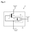
- Figure 2 shows a more detailed exemplary implementation of a composite switch suitable for use in a nested composite switch.
- composite switch 240 includes intermediate transistor 222 and LV transistor 224 cascoded with intermediate transistor 222.
- LV transistor 224 includes body diode 226.
- composite source 242, composite drain 244, and composite gate 246 are also shown in Figure 2 .
- Composite switch 240 having composite source 242, composite drain 244, and composite gate 246 corresponds to composite switch 140 having composite source 142, composite drain 144, and composite gate 146, in Figure 1 .
- LV transistor 224 may be implemented as an LV group IV transistor, such as a silicon transistor having a breakdown voltage of approximately 10V or less, such as 3V, for example. According to one implementation, LV transistor 224 may be a silicon MOSFET, for example, including body diode 226.
- Intermediate transistor 222 may be formed of III-N, and may be implemented as a HEMT or heterostructure FET (HFET), for example. According to one implementation, intermediate transistor 222 has a breakdown voltage greater than that of LV transistor 224 and less than that of primary transistor 110, in Figure 1 . More specifically, the breakdown voltage of intermediate transistor 222 is typically greater than the largest pinch-off voltage required to turn primary transistor 110 OFF.
- HFET heterostructure FET
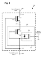
- FIG 3 shows an exemplary implementation of a nested composite switch including a primary transistor, and a composite switch corresponding generally to the implementation shown in Figure 2 .
- Nested composite switch 300 includes primary transistor 310 coupled to composite switch 340.
- composite switch 340 includes LV transistor 324 cascoded with intermediate transistor 322.
- LV transistor 324 includes body diode 326.
- nested composite source 302, nested composite drain 304, and nested composite gate 306 of nested composite switch 300 as well as source 312, drain 314, and gate 316 of primary transistor 310, and composite source 342, composite drain 344, and composite gate 346 of composite switch 340.
- Nested composite switch 300 having nested composite source 302, nested composite drain 304, and nested composite gate 306 corresponds to nested composite switch 100 having nested composite source 102, nested composite drain 104, and nested composite gate 106, and, in Figure 1 , and may share any of the characteristics previously attributed to those corresponding features, above.
- composite switch 340 having composite source 342, composite drain 344, and composite gate 346 corresponds to composite switch 240 having composite source 242, composite drain 244, and composite gate 246, in Figure 2 , and may share any of the characteristics previously attributed to those corresponding features.
- nested composite switch 300 can function in effect as a FET having nested composite source 302 and nested composite gate 306 provided by composite switch 340, and nested composite drain 304 provided by primary transistor 310.
- composite drain 344 of composite switch 340 is coupled to source 312 of primary transistor 310
- composite source 342 of composite switch 340 provides nested composite source 302 for nested composite switch 300
- composite gate 346 of composite switch 340 provides nested composite gate 306 for nested composite switch 300.
- drain 314 of primary transistor 310 provides nested composite drain 304 for nested composite switch 300
- gate 316 of primary transistor 310 is coupled to composite source 342 of composite switch 340.
- the implementation shown in Figure 3 advantageously provides nested composite switch 300 having increased switching speed and reduced on-state resistance when compared to conventional power devices with comparable voltage standoff capability. In some implementations, it may be advantageous to nest another high voltage or primary transistor with the nested composite switch shown in Figure 3 .
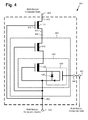
- An exemplary implementation of such a multi-nested composite switch is shown in Figure 4 .
- Multi-nested composite switch 401 includes higher voltage (HV+) primary transistor 411 coupled to nested composite switch 400.
- Nested composite switch 400 includes primary transistor 410 coupled to composite switch 440, and corresponds to nested composite switch 300 including primary transistor 310 coupled to composite switch 340, in Figure 3 .
- HV+ primary transistor refers to a primary transistor having a breakdown voltage equal to or greater than the breakdown voltage of primary transistor 410.
- HV+ primary transistor 411 and nested composite switch 400 are coupled using a cascode configuration to produce multi-nested composite switch 401. That is to say, nested composite drain 404 of nested composite switch 400 is coupled to source 413 of HV+ primary transistor 411, nested composite source 402 of nested composite switch 400 provides multi-nested composite source 403 for multi-nested composite switch 401, and nested composite gate 406 of nested composite switch 400 provides multi-nested composite gate 407 for multi-nested composite switch 401. Moreover, drain 415 of HV+ primary transistor 411 provides multi-nested composite drain 405 for multi-nested composite switch 401, while gate 417 of HV+ primary transistor 411 is coupled to nested composite source 402 of nested composite switch 400.
- the implementation shown in Figure 4 advantageously provides fast switching speed and low switching resistance analogous to the implementation in Figure 3 , while producing a higher breakdown voltage.
- package parasitics such as package inductances of the nested or multi-nested composite switch.
- package parasitics such as package inductances of the nested or multi-nested composite switch.
- one possible solution for reducing package parasitics for nested composite switch 300 is through monolithic integration of primary transistor 310 and/or composite switch 340.
- primary transistor 310, intermediate transistor 322, and LV transistor 324 may be monolithically integrated on a common composite semiconductor substrate designed to support both group IV and group III-V device fabrication.
- the present application discloses a nested composite switch having increased breakdown voltage.
- the implementations disclosed herein provide a nested switch having increased speed and reduced switching resistance when compared to conventional high voltage switches.
- the addition of an intermediate switch allows the use of a low voltage switch that would not otherwise be capable of adequately maintaining the primary switch in an OFF state within a cascode configuration.
Landscapes
- Junction Field-Effect Transistors (AREA)
- Electronic Switches (AREA)
- Semiconductor Integrated Circuits (AREA)
- Metal-Oxide And Bipolar Metal-Oxide Semiconductor Integrated Circuits (AREA)
Abstract
Description
- The present application claims the benefit of and priority to a pending provisional application entitled "Nested Composite Cascoded Device," Serial No.
61/506,529 filed on July 11, 2011 - As used herein, the phrase "group III-V" refers to a compound semiconductor that includes a group V element and at least one group III element. Moreover, the phrase "III-Nitride or III-N" refers to a compound semiconductor that includes nitrogen (N) and at least one group III element including aluminum (Al), gallium (Ga), indium (In), and boron (B), and including but not limited to any of its alloys, such as aluminum gallium nitride (AlxGa(1-x)N), indium gallium nitride (InyGa(1-y)N), aluminum indium gallium nitride (AlxInyGa(1-x-y)N), gallium arsenide phosphide nitride (GaAsaPbN(1-a-b)), and aluminum indium gallium arsenide phosphide nitride (AlxInyGa(1-x-y)AsaPbN(1-a-b)), for example. III-Nitride also refers generally to any polarity including but not limited to Ga-polar, N-polar, semi-polar or non-polar crystal orientations. A III-Nitride material may also include either the Wurtzitic, Zincblende or mixed polytypes, and may include single-crystal, monocrystalline, polycrystalline, or amorphous structures.
- Also as used herein, the phrase "group IV" refers to a semiconductor that includes at least one group four element including silicon (Si), germanium (Ge), and carbon (C), and also includes compound semiconductors such as SiGe and SiC, for example. Group IV may also refer to a semiconductor material which consists of layers of group IV elements or doping of group IV elements to produce strained silicon or other strained group IV material. In addition, group IV based composite substrates may include silicon on insulstor (SOI), separation by implantation of oxygen (SIMOX) process substrates, and silicon on sapphire (SOS), for example. Moreover, a group IV device may include devices formed using standard CMOS processing, but may also include NMOS and PMOS device processing.
- Furthermore, as used herein, the terms "LV device," "low voltage semiconductor device," "low voltage transistor, low voltage switch" and the like, refer to a low voltage device, with a typical breakdown voltage rating less than an "intermediate device," as described below. The LV device can include any suitable semiconductor material that forms a field-effect transistor (FET) such as an insulated-gate FET (IGFET), for example. Suitable semiconductor materials include group IV semiconductor materials such as Si, strained silicon, SiGe, SiC, and group III-V materials including III-As, III-P, III-Nitride or any of their alloys.
- Additionally, the term "intermediate device, intermediate transistor and intermediate switch" refers to a device with a typical breakdown voltage greater than the LV device and less than a "primary device". The "primary device, primary transistor or primary switch" refers to a device with a typical breakdown voltage greater than both the intermediate device and the LV device.
- In high power and high performance switching applications, group III-V field-effect transistors (FETs) and high mobility electron transistors (HEMTs), such as III-Nitride FETs and III-Nitride HEMTs, are often desirable for their high efficiency and high-voltage operation. Moreover, it is often desirable to combine such group III-V transistors with other FETs, such as group IV FETs, to create high performance composite switches.
- In power management applications where normally OFF characteristics of power devices are desirable, a depletion mode (normally ON) III-Nitride or other group III-V transistor can be cascoded with an enhancement mode (normally OFF) low-voltage (LV) group IV transistor, for example a silicon FET, to produce an enhancement mode (normally OFF) composite power switch. However, the performance of the composite switch can be limited by the on-state and voltage breakdown characteristics of the LV group IV transistor used. In particular, the breakdown voltage for a given on-state resistance of the LV group IV transistor may be insufficient to support the required pinch-off voltage required to maintain the group III-V transistor in a satisfactorily OFF condition.
- The present disclosure is directed to a nested composite switch, substantially as shown in and/or described in connection with at least one of the figures, and as set forth more completely in the claims.
-
-
Figure 1 presents a diagram showing one exemplary implementation of a nested composite switch including a primary transistor and a composite switch. -
Figure 2 presents a diagram showing a more detailed exemplary implementation of a composite switch suitable for use in a nested composite switch. -
Figure 3 presents a diagram showing an exemplary implementation of a nested composite switch including a primary transistor, and a composite switch corresponding generally to the implementation shown inFigure 2 . -
Figure 4 presents a diagram showing an exemplary implementation of a multi-nested composite switch. - The following description contains specific information pertaining to implementations in the present disclosure. One skilled in the art will recognize that the present disclosure may be implemented in a manner different from that specifically discussed herein. The drawings in the present application and their accompanying detailed description are directed to merely exemplary implementations. Unless noted otherwise, like or corresponding elements among the figures may be indicated by like or corresponding reference numerals. Moreover, the drawings and illustrations in the present application are generally not to scale, and are not intended to correspond to actual relative dimensions.
- Group III-V semiconductors include III-Nitride materials formed of gallium nitride (GaN) and/or its alloys, such as aluminum gallium nitride (AlGaN), indium gallium nitride (InGaN), and aluminum indium gallium nitride (AlInGaN). These materials are semiconductor compounds that have a relatively wide, direct bandgap and strong piezoelectric polarizations, and can support high breakdown fields, high saturation velocities, and the creation of two-dimensional electron gases (2DEGs). As a result, III-Nitride materials such as GaN are used in many microelectronic applications such as depletion mode (e.g., normally ON) power field-effect transistors (FETs) and high electron mobility transistors (HEMTs).
- As noted above, in power management applications where normally OFF characteristics of power devices are desirable, a depletion mode (normally ON) III-Nitride or other group III-V transistor can be cascoded with an enhancement mode (normally OFF) low voltage (LV) transistor, such as a silicon or other LV group IV transistor, to produce an enhancement mode composite power switch. However, the performance of the composite switch can be limited by the on-state and voltage breakdown characteristics of the LV group IV transistor used. In particular, the breakdown voltage for a given on-state resistance of the LV group IV transistor may be insufficient to support the required pinch-off voltage required to maintain the group III-V transistor in a satisfactorily OFF condition. In such a case, an intermediate III-V transistor may be used in a nested cascode configuration.
- The present application is directed to a nested composite switch capable of providing enhanced voltage breakdown resistance while providing advantages such as fast switching speed, high transconductance, low switching charge, low threshold voltage, and low on-state resistance typically associated with an LV transistor.
- According to one implementation, the nested composite switch includes a primary transistor coupled to a composite switch. The composite switch may include an LV transistor cascoded with an intermediate transistor (for example a depletion mode or normally ON III-N transistor) having a breakdown voltage greater than that that of the LV transistor and less than that of the primary transistor. Moreover, in one implementation, the composite switch including the LV transistor, which may be a normally OFF composite switch, can be cascoded with the primary transistor. The cascoded combination of the normally OFF composite switch with the primary transistor, which may be a normally ON III-Nitride or other group III-V device, for example, can be implemented to produce a normally OFF nested composite switch having an increased speed and breakdown voltage, and a reduced on-state resistance.
-
Figure 1 shows one exemplary implementation of a nested composite switch including a primary transistor and a composite switch. As shown inFigure 1 ,nested composite switch 100 includesprimary transistor 110 andcomposite switch 140 coupled toprimary transistor 110. As further shown inFigure 1 ,nested composite switch 100 hasnested composite source 102,nested composite drain 104, and nestedcomposite gate 106. Also shown inFigure 1 aresource 112,drain 114, andgate 116 ofprimary transistor 110, andcomposite source 142,composite drain 144, andcomposite gate 146 ofcomposite switch 140. - Referring now to
Figure 2, Figure 2 shows a more detailed exemplary implementation of a composite switch suitable for use in a nested composite switch. As shown inFigure 2 ,composite switch 240 includesintermediate transistor 222 andLV transistor 224 cascoded withintermediate transistor 222. As further shown inFigure 2 ,LV transistor 224 includesbody diode 226. Also shown inFigure 2 arecomposite source 242,composite drain 244, andcomposite gate 246.Composite switch 240 havingcomposite source 242,composite drain 244, andcomposite gate 246 corresponds tocomposite switch 140 havingcomposite source 142,composite drain 144, andcomposite gate 146, inFigure 1 . -
LV transistor 224 may be implemented as an LV group IV transistor, such as a silicon transistor having a breakdown voltage of approximately 10V or less, such as 3V, for example. According to one implementation,LV transistor 224 may be a silicon MOSFET, for example, includingbody diode 226. -
Intermediate transistor 222 may be formed of III-N, and may be implemented as a HEMT or heterostructure FET (HFET), for example. According to one implementation,intermediate transistor 222 has a breakdown voltage greater than that ofLV transistor 224 and less than that ofprimary transistor 110, inFigure 1 . More specifically, the breakdown voltage ofintermediate transistor 222 is typically greater than the largest pinch-off voltage required to turnprimary transistor 110 OFF. -
Figure 3 shows an exemplary implementation of a nested composite switch including a primary transistor, and a composite switch corresponding generally to the implementation shown inFigure 2 . Nestedcomposite switch 300 includesprimary transistor 310 coupled tocomposite switch 340. As shown inFigure 3 ,composite switch 340 includesLV transistor 324 cascoded withintermediate transistor 322. As further shown inFigure 3 ,LV transistor 324 includesbody diode 326. Also shown inFigure 3 are nestedcomposite source 302, nestedcomposite drain 304, and nestedcomposite gate 306 of nestedcomposite switch 300, as well assource 312, drain 314, andgate 316 ofprimary transistor 310, andcomposite source 342,composite drain 344, and composite gate 346 ofcomposite switch 340. - Nested
composite switch 300 having nestedcomposite source 302, nestedcomposite drain 304, and nestedcomposite gate 306 corresponds to nestedcomposite switch 100 having nestedcomposite source 102, nestedcomposite drain 104, and nestedcomposite gate 106, and, inFigure 1 , and may share any of the characteristics previously attributed to those corresponding features, above. In addition,composite switch 340 havingcomposite source 342,composite drain 344, and composite gate 346 corresponds tocomposite switch 240 havingcomposite source 242,composite drain 244, andcomposite gate 246, inFigure 2 , and may share any of the characteristics previously attributed to those corresponding features. -
Primary transistor 310 andcomposite switch 340 are coupled using a cascode configuration to produce nestedcomposite switch 300, which according to the implementation shown inFigure 3 results in a composite three terminal device. As a result, nestedcomposite switch 300 can function in effect as a FET having nestedcomposite source 302 and nestedcomposite gate 306 provided bycomposite switch 340, and nestedcomposite drain 304 provided byprimary transistor 310. In other words,composite drain 344 ofcomposite switch 340 is coupled tosource 312 ofprimary transistor 310,composite source 342 ofcomposite switch 340 provides nestedcomposite source 302 for nestedcomposite switch 300, and composite gate 346 ofcomposite switch 340 provides nestedcomposite gate 306 for nestedcomposite switch 300. Moreover, drain 314 ofprimary transistor 310 provides nestedcomposite drain 304 for nestedcomposite switch 300, whilegate 316 ofprimary transistor 310 is coupled tocomposite source 342 ofcomposite switch 340. - The implementation shown in
Figure 3 advantageously provides nestedcomposite switch 300 having increased switching speed and reduced on-state resistance when compared to conventional power devices with comparable voltage standoff capability. In some implementations, it may be advantageous to nest another high voltage or primary transistor with the nested composite switch shown inFigure 3 . An exemplary implementation of such a multi-nested composite switch is shown inFigure 4 . - Multi-nested
composite switch 401 includes higher voltage (HV+)primary transistor 411 coupled to nestedcomposite switch 400. Nestedcomposite switch 400 includesprimary transistor 410 coupled tocomposite switch 440, and corresponds to nestedcomposite switch 300 includingprimary transistor 310 coupled tocomposite switch 340, inFigure 3 . As used herein, "HV+ primary transistor" refers to a primary transistor having a breakdown voltage equal to or greater than the breakdown voltage ofprimary transistor 410. - According to the implementation shown in
Figure 4 , HV+primary transistor 411 and nestedcomposite switch 400 are coupled using a cascode configuration to produce multi-nestedcomposite switch 401. That is to say, nestedcomposite drain 404 of nestedcomposite switch 400 is coupled tosource 413 of HV+primary transistor 411, nestedcomposite source 402 of nestedcomposite switch 400 provides multi-nestedcomposite source 403 for multi-nestedcomposite switch 401, and nestedcomposite gate 406 of nestedcomposite switch 400 provides multi-nestedcomposite gate 407 for multi-nestedcomposite switch 401. Moreover, drain 415 of HV+primary transistor 411 provides multi-nestedcomposite drain 405 for multi-nestedcomposite switch 401, whilegate 417 of HV+primary transistor 411 is coupled to nestedcomposite source 402 of nestedcomposite switch 400. - The implementation shown in
Figure 4 advantageously provides fast switching speed and low switching resistance analogous to the implementation inFigure 3 , while producing a higher breakdown voltage. In yet other implementations, it may be desirable to repeat this nesting of cascoded composite switches including one normally OFF LV group IV transistor and several normally ON group III-V transistors to produce a normally OFF multi-nested composite switch capable of very high voltage operation. - In some implementations, it may further be desirable to reduce package parasitics, such as package inductances of the nested or multi-nested composite switch. Referring back to
Figure 3 , for example, one possible solution for reducing package parasitics for nestedcomposite switch 300 is through monolithic integration ofprimary transistor 310 and/orcomposite switch 340. In other words,primary transistor 310,intermediate transistor 322, andLV transistor 324 may be monolithically integrated on a common composite semiconductor substrate designed to support both group IV and group III-V device fabrication. - Thus, by coupling a primary transistor to a composite switch including an LV transistor cascoded with an intermediate transistor, the present application discloses a nested composite switch having increased breakdown voltage. Moreover, when implemented so as to use the LV transistor to control current through the primary transistor, the implementations disclosed herein provide a nested switch having increased speed and reduced switching resistance when compared to conventional high voltage switches. The addition of an intermediate switch allows the use of a low voltage switch that would not otherwise be capable of adequately maintaining the primary switch in an OFF state within a cascode configuration.
- From the above description it is manifest that various techniques can be used for implementing the concepts described in the present application without departing from the scope of those concepts. Moreover, while the concepts have been described with specific reference to certain implementations, a person of ordinary skill in the art would recognize that changes can be made in form and detail without departing from the scope of those concepts. As such, the described implementations are to be considered in all respects as illustrative and not restrictive. It should also be understood that the present application is not limited to the particular implementations described herein, but many rearrangements, modifications, and substitutions are possible without departing from the scope of the present disclosure.
Claims (15)
- A nested composite switch comprising:a normally ON primary transistor coupled to a composite switch;said composite switch including a low voltage (LV) transistor cascoded with an intermediate transistor having a breakdown voltage greater than said LV transistor and less than said normally ON primary transistor.
- The nested composite switch of claim 1, wherein said normally ON primary transistor is a group III-V transistor.
- The nested composite switch of claim 1, wherein said normally ON primary transistor is one of a III-Nitride heterostructure field-effect transistor (HFET) and a high electron mobility transistor (HEMT).
- The nested composite switch of claim 1, wherein said composite switch is a normally OFF composite switch.
- The nested composite switch of claim 1, wherein said LV transistor is an LV group IV transistor.
- The nested composite switch of claim 1, wherein said nested composite switch is normally OFF.
- The nested composite switch of claim 1, wherein said nested composite switch is monolithically integrated.
- The nested composite switch of claim 1, wherein at least two of said normally ON primary transistor, said intermediate transistor, and said LV transistor are monolithically integrated.
- The nested composite switch of claim 1, wherein a composite drain of said composite switch is coupled to a source of said normally ON primary transistor, a composite source of said composite switch provides a nested composite source for said nested composite switch, and a composite gate of said composite switch provides a nested composite gate for said nested composite switch;
a drain of said normally ON primary transistor provides a nested composite drain for said nested composite switch, and a gate of said normally ON primary transistor is coupled to said composite source of said composite switch. - The nested composite switch of claim 1, wherein said nested composite switch is cascoded with at least one higher voltage (HV+) primary transistor.
- A nested composite switch comprising:a normally ON primary transistor coupled to a normally OFF composite switch;said normally OFF composite switch including a low voltage (LV) transistor cascoded with an intermediate transistor having a breakdown voltage greater than said LV transistor and less than said normally ON primary transistor.
- The nested composite switch of claim 11, wherein said normally ON primary transistor is a normally ON group III-V transistor.
- The nested composite switch of claim 11, wherein said normally ON primary transistor is one of a III-Nitride heterostructure field-effect transistor (HFET) and a high electron mobility transistor (HEMT).
- The nested composite switch of claim 11, wherein said nested composite switch is cascoded with at least one higher voltage (HV+) primary transistor.
- A nested composite switch comprising:a primary group III-V transistor coupled to a composite switch;said composite switch including a low voltage (LV) group IV transistor cascoded with an intermediate group III-V transistor having a breakdown voltage greater than said LV group IV transistor and less than said primary group III-V transistor.
Applications Claiming Priority (2)
| Application Number | Priority Date | Filing Date | Title |
|---|---|---|---|
| US201161506529P | 2011-07-11 | 2011-07-11 | |
| US13/542,194 US8988133B2 (en) | 2011-07-11 | 2012-07-05 | Nested composite switch |
Publications (2)
| Publication Number | Publication Date |
|---|---|
| EP2546987A2 true EP2546987A2 (en) | 2013-01-16 |
| EP2546987A3 EP2546987A3 (en) | 2013-02-20 |
Family
ID=46799997
Family Applications (1)
| Application Number | Title | Priority Date | Filing Date |
|---|---|---|---|
| EP12175467A Withdrawn EP2546987A3 (en) | 2011-07-11 | 2012-07-06 | Nested Composite Switch |
Country Status (3)
| Country | Link |
|---|---|
| US (1) | US8988133B2 (en) |
| EP (1) | EP2546987A3 (en) |
| JP (1) | JP2013038406A (en) |
Cited By (2)
| Publication number | Priority date | Publication date | Assignee | Title |
|---|---|---|---|---|
| EP2824700A1 (en) * | 2013-07-12 | 2015-01-14 | International Rectifier Corporation | Monolithic composite iii-nitride transistor with high voltage group iv enable switch |
| US12408383B2 (en) | 2018-10-18 | 2025-09-02 | Semiconductor Energy Laboratory Co., Ltd. | Semiconductor device, semiconductor wafer, and electronic device |
Families Citing this family (6)
| Publication number | Priority date | Publication date | Assignee | Title |
|---|---|---|---|---|
| US9219058B2 (en) * | 2010-03-01 | 2015-12-22 | Infineon Technologies Americas Corp. | Efficient high voltage switching circuits and monolithic integration of same |
| US8981380B2 (en) * | 2010-03-01 | 2015-03-17 | International Rectifier Corporation | Monolithic integration of silicon and group III-V devices |
| US8816264B2 (en) * | 2012-07-31 | 2014-08-26 | Omnivision Technologies, Inc. | CMOS image sensor switch circuit for reduced charge injection |
| US20150014784A1 (en) * | 2013-07-12 | 2015-01-15 | Delta Electronics, Inc. | Cascode switch device |
| US9406674B2 (en) | 2013-07-12 | 2016-08-02 | Infineon Technologies Americas Corp. | Integrated III-nitride D-mode HFET with cascoded pair half bridge |
| JP7455604B2 (en) | 2020-02-14 | 2024-03-26 | 株式会社東芝 | Normally-on transistor drive circuit and drive method |
Citations (1)
| Publication number | Priority date | Publication date | Assignee | Title |
|---|---|---|---|---|
| DE102004006537A1 (en) * | 2003-02-13 | 2004-08-26 | Denso Corp., Kariya | Semiconductor device formed by a silicon carbide substrate and method of manufacturing the same |
Family Cites Families (14)
| Publication number | Priority date | Publication date | Assignee | Title |
|---|---|---|---|---|
| JPS59223027A (en) * | 1983-06-02 | 1984-12-14 | Oki Electric Ind Co Ltd | Semiconductor logical circuit |
| US6483369B1 (en) * | 2001-10-02 | 2002-11-19 | Technical Witts Inc. | Composite mosfet cascode switches for power converters |
| JP3847620B2 (en) | 2001-12-26 | 2006-11-22 | 日本テキサス・インスツルメンツ株式会社 | Driving circuit |
| US8089097B2 (en) * | 2002-12-27 | 2012-01-03 | Momentive Performance Materials Inc. | Homoepitaxial gallium-nitride-based electronic devices and method for producing same |
| US6865093B2 (en) * | 2003-05-27 | 2005-03-08 | Power Integrations, Inc. | Electronic circuit control element with tap element |
| JP4645313B2 (en) | 2005-06-14 | 2011-03-09 | 富士電機システムズ株式会社 | Semiconductor device |
| JP5358882B2 (en) * | 2007-02-09 | 2013-12-04 | サンケン電気株式会社 | Composite semiconductor device including rectifying element |
| JP2009182107A (en) * | 2008-01-30 | 2009-08-13 | Furukawa Electric Co Ltd:The | Semiconductor device |
| US8957642B2 (en) | 2008-05-06 | 2015-02-17 | International Rectifier Corporation | Enhancement mode III-nitride switch with increased efficiency and operating frequency |
| US9502973B2 (en) | 2009-04-08 | 2016-11-22 | Infineon Technologies Americas Corp. | Buck converter with III-nitride switch for substantially increased input-to-output voltage ratio |
| US8269259B2 (en) | 2009-12-07 | 2012-09-18 | International Rectifier Corporation | Gated AlGaN/GaN heterojunction Schottky device |
| US8455948B2 (en) * | 2011-01-07 | 2013-06-04 | Infineon Technologies Austria Ag | Transistor arrangement with a first transistor and with a plurality of second transistors |
| US20130175542A1 (en) | 2011-04-11 | 2013-07-11 | International Rectifier Corporation | Group III-V and Group IV Composite Diode |
| US20130015501A1 (en) | 2011-07-11 | 2013-01-17 | International Rectifier Corporation | Nested Composite Diode |
-
2012
- 2012-07-05 US US13/542,194 patent/US8988133B2/en not_active Expired - Fee Related
- 2012-07-06 JP JP2012152933A patent/JP2013038406A/en active Pending
- 2012-07-06 EP EP12175467A patent/EP2546987A3/en not_active Withdrawn
Patent Citations (1)
| Publication number | Priority date | Publication date | Assignee | Title |
|---|---|---|---|---|
| DE102004006537A1 (en) * | 2003-02-13 | 2004-08-26 | Denso Corp., Kariya | Semiconductor device formed by a silicon carbide substrate and method of manufacturing the same |
Cited By (3)
| Publication number | Priority date | Publication date | Assignee | Title |
|---|---|---|---|---|
| EP2824700A1 (en) * | 2013-07-12 | 2015-01-14 | International Rectifier Corporation | Monolithic composite iii-nitride transistor with high voltage group iv enable switch |
| US9184243B2 (en) | 2013-07-12 | 2015-11-10 | Infineon Technologies Americas Corp. | Monolithic composite III-nitride transistor with high voltage group IV enable switch |
| US12408383B2 (en) | 2018-10-18 | 2025-09-02 | Semiconductor Energy Laboratory Co., Ltd. | Semiconductor device, semiconductor wafer, and electronic device |
Also Published As
| Publication number | Publication date |
|---|---|
| US20130015905A1 (en) | 2013-01-17 |
| JP2013038406A (en) | 2013-02-21 |
| EP2546987A3 (en) | 2013-02-20 |
| US8988133B2 (en) | 2015-03-24 |
Similar Documents
| Publication | Publication Date | Title |
|---|---|---|
| US9397089B2 (en) | Group III-V HEMT having a selectably floating substrate | |
| US9041067B2 (en) | Integrated half-bridge circuit with low side and high side composite switches | |
| EP2546986A2 (en) | Nested Composite Diode | |
| US9859882B2 (en) | High voltage composite semiconductor device with protection for a low voltage device | |
| US8988133B2 (en) | Nested composite switch | |
| US9406674B2 (en) | Integrated III-nitride D-mode HFET with cascoded pair half bridge | |
| US8766375B2 (en) | Composite semiconductor device with active oscillation prevention | |
| US9310819B2 (en) | Power converter including integrated driver providing overcurrent protection | |
| US9349715B2 (en) | Depletion mode group III-V transistor with high voltage group IV enable switch | |
| US20150162832A1 (en) | Group III-V Voltage Converter with Monolithically Integrated Level Shifter, High Side Driver, and High Side Power Switch | |
| US10083884B2 (en) | Compact high-voltage semiconductor package | |
| US20140070627A1 (en) | Integrated Group III-V Power Stage | |
| US20120241820A1 (en) | III-Nitride Transistor with Passive Oscillation Prevention | |
| US20150162321A1 (en) | Composite Power Device with ESD Protection Clamp | |
| EP2503692B1 (en) | Composite Semiconductor Device with Higher Threshold Voltage | |
| US9438112B2 (en) | Power converter including integrated driver for depletion mode group III-V transistor | |
| US9236376B2 (en) | Power semiconductor device with oscillation prevention | |
| US20140239349A1 (en) | Drain Pad Having a Reduced Termination Electric Field |
Legal Events
| Date | Code | Title | Description |
|---|---|---|---|
| PUAI | Public reference made under article 153(3) epc to a published international application that has entered the european phase |
Free format text: ORIGINAL CODE: 0009012 |
|
| AK | Designated contracting states |
Kind code of ref document: A2 Designated state(s): AL AT BE BG CH CY CZ DE DK EE ES FI FR GB GR HR HU IE IS IT LI LT LU LV MC MK MT NL NO PL PT RO RS SE SI SK SM TR |
|
| AX | Request for extension of the european patent |
Extension state: BA ME |
|
| PUAL | Search report despatched |
Free format text: ORIGINAL CODE: 0009013 |
|
| AK | Designated contracting states |
Kind code of ref document: A3 Designated state(s): AL AT BE BG CH CY CZ DE DK EE ES FI FR GB GR HR HU IE IS IT LI LT LU LV MC MK MT NL NO PL PT RO RS SE SI SK SM TR |
|
| AX | Request for extension of the european patent |
Extension state: BA ME |
|
| RIC1 | Information provided on ipc code assigned before grant |
Ipc: H03K 17/30 20060101AFI20130115BHEP Ipc: H03K 17/16 20060101ALI20130115BHEP Ipc: H03K 17/567 20060101ALI20130115BHEP Ipc: H01L 27/06 20060101ALI20130115BHEP Ipc: H03K 17/10 20060101ALI20130115BHEP Ipc: H01L 29/00 20060101ALI20130115BHEP |
|
| 17P | Request for examination filed |
Effective date: 20130820 |
|
| RBV | Designated contracting states (corrected) |
Designated state(s): AL AT BE BG CH CY CZ DE DK EE ES FI FR GB GR HR HU IE IS IT LI LT LU LV MC MK MT NL NO PL PT RO RS SE SI SK SM TR |
|
| 17Q | First examination report despatched |
Effective date: 20180305 |
|
| RAP1 | Party data changed (applicant data changed or rights of an application transferred) |
Owner name: INFINEON TECHNOLOGIES AMERICAS CORP. |
|
| STAA | Information on the status of an ep patent application or granted ep patent |
Free format text: STATUS: THE APPLICATION IS DEEMED TO BE WITHDRAWN |
|
| 18D | Application deemed to be withdrawn |
Effective date: 20180717 |