EP2545586B1 - Graphene based three-dimensional integrated circuit device - Google Patents
Graphene based three-dimensional integrated circuit device Download PDFInfo
- Publication number
- EP2545586B1 EP2545586B1 EP11753755.5A EP11753755A EP2545586B1 EP 2545586 B1 EP2545586 B1 EP 2545586B1 EP 11753755 A EP11753755 A EP 11753755A EP 2545586 B1 EP2545586 B1 EP 2545586B1
- Authority
- EP
- European Patent Office
- Prior art keywords
- graphene
- layer
- gate
- level
- field effect
- Prior art date
- Legal status (The legal status is an assumption and is not a legal conclusion. Google has not performed a legal analysis and makes no representation as to the accuracy of the status listed.)
- Active
Links
Images



Classifications
-
- H—ELECTRICITY
- H10—SEMICONDUCTOR DEVICES; ELECTRIC SOLID-STATE DEVICES NOT OTHERWISE PROVIDED FOR
- H10D—INORGANIC ELECTRIC SEMICONDUCTOR DEVICES
- H10D88/00—Three-dimensional [3D] integrated devices
-
- H—ELECTRICITY
- H10—SEMICONDUCTOR DEVICES; ELECTRIC SOLID-STATE DEVICES NOT OTHERWISE PROVIDED FOR
- H10D—INORGANIC ELECTRIC SEMICONDUCTOR DEVICES
- H10D84/00—Integrated devices formed in or on semiconductor substrates that comprise only semiconducting layers, e.g. on Si wafers or on GaAs-on-Si wafers
- H10D84/01—Manufacture or treatment
- H10D84/02—Manufacture or treatment characterised by using material-based technologies
-
- H—ELECTRICITY
- H10—SEMICONDUCTOR DEVICES; ELECTRIC SOLID-STATE DEVICES NOT OTHERWISE PROVIDED FOR
- H10D—INORGANIC ELECTRIC SEMICONDUCTOR DEVICES
- H10D84/00—Integrated devices formed in or on semiconductor substrates that comprise only semiconducting layers, e.g. on Si wafers or on GaAs-on-Si wafers
- H10D84/80—Integrated devices formed in or on semiconductor substrates that comprise only semiconducting layers, e.g. on Si wafers or on GaAs-on-Si wafers characterised by the integration of at least one component covered by groups H10D12/00 or H10D30/00, e.g. integration of IGFETs
- H10D84/82—Integrated devices formed in or on semiconductor substrates that comprise only semiconducting layers, e.g. on Si wafers or on GaAs-on-Si wafers characterised by the integration of at least one component covered by groups H10D12/00 or H10D30/00, e.g. integration of IGFETs of only field-effect components
- H10D84/83—Integrated devices formed in or on semiconductor substrates that comprise only semiconducting layers, e.g. on Si wafers or on GaAs-on-Si wafers characterised by the integration of at least one component covered by groups H10D12/00 or H10D30/00, e.g. integration of IGFETs of only field-effect components of only insulated-gate FETs [IGFET]
-
- H—ELECTRICITY
- H10—SEMICONDUCTOR DEVICES; ELECTRIC SOLID-STATE DEVICES NOT OTHERWISE PROVIDED FOR
- H10D—INORGANIC ELECTRIC SEMICONDUCTOR DEVICES
- H10D62/00—Semiconductor bodies, or regions thereof, of devices having potential barriers
- H10D62/80—Semiconductor bodies, or regions thereof, of devices having potential barriers characterised by the materials
- H10D62/881—Semiconductor bodies, or regions thereof, of devices having potential barriers characterised by the materials being a two-dimensional material
- H10D62/882—Graphene
-
- Y—GENERAL TAGGING OF NEW TECHNOLOGICAL DEVELOPMENTS; GENERAL TAGGING OF CROSS-SECTIONAL TECHNOLOGIES SPANNING OVER SEVERAL SECTIONS OF THE IPC; TECHNICAL SUBJECTS COVERED BY FORMER USPC CROSS-REFERENCE ART COLLECTIONS [XRACs] AND DIGESTS
- Y10—TECHNICAL SUBJECTS COVERED BY FORMER USPC
- Y10S—TECHNICAL SUBJECTS COVERED BY FORMER USPC CROSS-REFERENCE ART COLLECTIONS [XRACs] AND DIGESTS
- Y10S977/00—Nanotechnology
- Y10S977/70—Nanostructure
- Y10S977/755—Nanosheet or quantum barrier/well, i.e. layer structure having one dimension or thickness of 100 nm or less
Definitions
- the present invention relates generally to semiconductor device manufacturing and, more particularly, to a graphene based, three-dimensional (3D) integrated circuit device.
- Graphene refers to a two-dimensional planar sheet of carbon atoms arranged in a hexagonal benzene-ring structure.
- a free-standing graphene structure is theoretically stable only in a two-dimensional space, which implies that a truly planar graphene structure does not exist in a three-dimensional space, being unstable with respect to formation of curved structures such as soot, fullerenes, nanotubes or buckled two dimensional structures.
- a two-dimensional graphene structure may be stable when supported on a substrate, for example, on the surface of a silicon carbide (SiC) crystal. Free standing graphene films have also been produced, but they may not have the idealized flat geometry.
- graphene has hybrid orbitals formed by sp 2 hybridization.
- the 2s orbital and two of the three 2p orbitals mix to form three sp 2 orbitals.
- the one remaining p-orbital forms a pi ( ⁇ )-bond between the carbon atoms.
- the structure of graphene has a conjugated ring of the p-orbitals, i.e., the graphene structure is aromatic.
- graphene is only one atomic layer thin.
- Graphene has an unusual band structure in which conical electron and hole pockets meet only at the K-points of the Brillouin zone in momentum space.
- the energy of the charge carriers, i.e., electrons or holes, has a linear dependence on the momentum of the carriers.
- the carriers behave as relativistic Dirac-Fermions with a zero effective mass and are governed by Dirac's equation.
- Graphene sheets may have a large carrier mobility of greater than 200,000 cm 2 /V-sec at 4K. Even at 300K, the carrier mobility can be as high as 15,000 cm 2 /V-sec.
- Graphene layers may be grown by solid-state graphitization, i.e., by sublimating silicon atoms from a surface of a silicon carbide crystal, such as the (0001) surface. At about 1,150°C, a complex pattern of surface reconstruction begins to appear at an initial stage of graphitization. Typically, a higher temperature is needed to form a graphene layer.
- Graphene layers on another material are also known in the art. For example, single or several layers of graphene maybe formed on a metal surface, such as copper and nickel, by chemical deposition of carbon atoms from a carbon-rich precursor.
- Graphene displays many other advantageous electrical properties such as electronic coherence at near room temperature and quantum interference effects. Ballistic transport properties in small scale structures are also expected in graphene layers.
- graphene is ultimately promising for electronic applications.
- graphene transistors have been demonstrated recently, and more advanced graphene circuits arc considered to be promising candidates to perhaps replace silicon in future integrated circuit technology.
- J. Meindl et al. “Nanoelectronics in Retrospect, Prospect and Principle", ISSCC 2010, pages 31-35 , it is reported that graphene demonstrated capability to serve as the source, channel and drain regions of a field effect transistor and as an interconnect.
- a method of forming a three-dimensional (3D) integrated circuit (IC) structure according to claim 2.
- a 3D integrated circuit (1C) generally refers to a chip having two or more layers of active electronic components, integrated both vertically and horizontally into a single circuit.
- 3D ICs potentially offer many significant benefits, such as for example: a smaller footprint (more functionality fitting into a small space), speed (the average wire length becomes much shorter, in turn reducing signal propagation delay and increasing overall performance), power consumption (by keeping a signal on-chip, the resulting shorter wires reduce power consumption and produce less parasitic capacitance), and heterogeneous integration, to name a few.
- different circuit layers may be formed with different processes, or even on different types of wafers.
- components otherwise having completely incompatible manufacturing processes could be combined in a single device.
- 3D ICs may be formed by techniques such as wafer-on-wafer bonding, wherein electronic components are built on two or more semiconductor wafers, which are then aligned, bonded, and diced into 3D ICs. Each wafer may be thinned before or after bonding. Vertical connections are either built into the wafers before bonding or otherwise created in the stack after bonding. These "through-silicon vias" (TSVs) pass through the silicon substrate(s) between active layers and/or between an active layer and an external bond pad.
- TSVs through-silicon vias
- electronic components are built on two semiconductor wafers. One wafer is diced, and the singulated dies are aligned and bonded onto die sites of the second wafer.
- thinning and TSV creation are performed either before or after bonding. Additional dies may be added to the stacks before dicing. Alternatively, in a die-on-die process, electronic components are built on multiple dies, which are then aligned and bonded. Thinning and TSV creation may be done before or after bonding.
- 3D ICs In order to avoid multiple substrates and aligning, thinning, bonding, or TSV techniques, 3D ICs would desirably be formed monolithically. That is, the electronic components and their connections (wiring) are built in layers on a single semiconductor wafer, which is then diced into 3D ICs. Unfortunately, existing applications of this method are currently limited because creating conventional transistors in semiconductor layers (e.g., dopant implantation and activation annealing) requires processing temperatures that are sufficient any existing wiring.
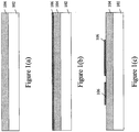
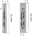
- Figures 1(a) through 1(h) are a series of cross-sectional views illustrating a method of forming a graphene based, three-dimensional (3D) integrated circuit.
- a starting substrate 102 e.g., silicon
- an insulating layer e.g., an oxide such as SiO 2
- a blanket graphene layer 106 is transferred onto the insulating layer 104.
- the transfer of graphene films may be performed in any suitable manner known in the art such as, for example, by a dry thermal release tape process.
- graphene is deposited on such a substrate surface in this manner, it is a particularly suitable material for 3D integration.
- the graphene layer 106 is patterned through appropriate lithography techniques (e.g., hardmask and/or photoresist layer formation, development and etching) to form desired active areas of graphene-based devices. This is followed by a first level of transistor device formation. As shown in Figure 1(d) , the graphene active areas 106 are covered with transistor gate stack materials such as, for example, a gate dielectric layer 108 and a gate electrode layer 110.
- the gate dielectric layer 108 may be a high-k material such as hafnium, hafnium silicate, zirconium oxide, zirconium silicate, nitrided dielectrics, as well as combinations thereof.
- the gate electrode layer 110 may include polysilicon, a metal, or combinations thereof.
- the gate dielectric and gate electrode layers 108, 110 are then patterned so as to define transistor devices (e.g., field effect transistors or FETs) on the patterned graphene active areas 106, including gate electrodes 112 and gate dielectric layers 114.
- transistor devices e.g., field effect transistors or FETs
- FETs field effect transistors
- the patterning operation depicted in the figures is only illustrative in nature, in that more than one patterning and RIE process may be used, for example, in accordance with different gate stack requirements depending on the type and polarity of the transistor device.
- the designation "GN” refers to a transistor gate for an n-type device (e.g., an NFET) while the designation "GP” refers to a transistor gate for a p-type device (e.g., a PFET).
- Source/drain contacts 116 and conductive pad structures 118 is shown in Figure 1(f) .
- the formation of the source and drain contacts includes, for example deposition of source/drain contact material and patterning.
- the source/drain contact material may be a metal material such as, for example, titanium (Ti), palladium (Pd), aluminum (Al), tungsten (W), or alloys thereof.
- the deposition method can be may include, for example, sputtering, and atomic layer deposition (ALD).
- an insulating layer 120 (e.g., an oxide) is formed over the devices as shown in Figure 1(g) .
- Vias 122 are then etched into the insulating layer 120 so as to provide vertical electrical connection to one or more additional levels of graphene based active devices, in accordance with a 3D IC structure.
- the lower level 124 of graphene based active devices is shown connected to an upper layer 126 of graphene based active devices.
- the formation of the upper level 126 is similar to that of the lower level 124, in that a graphene layer (e.g., monolayer) is first deposited/transferred onto the completed lower level 124, followed by pattering of the desired active areas of the graphene, formation and patterning of the gate stack materials, formation and patterning of the source/drain contacts and conductive pads, and formation of an insulating layer over the upper level devices.
- a graphene layer e.g., monolayer
- each level of graphene may have different functions (e.g., logic, analog, memory).
- the 3D IC device shown in the process flow sequence of Figures 1(a) through 1(h) is an example of a top gate orientation, in that the gate electrode and dielectric are disposed above the active graphene source/drain regions.
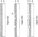
- the active graphene devices are formed using a bottom orientation, as depicted in the process flow sequence of Figures 2(a) through 2(k) .
- a starting substrate 202 e.g., silicon
- an insulating layer e.g., an oxide such as SiO 2
- the insulating layer 204 is instead patterned with vias 206 corresponding to the locations of the gates of the lower level graphene based devices, as shown in Figure 2(b) .
- a gate electrode layer 208 is formed over the device, filling in the vias.
- individual gate electrodes 210 are now defined, as shown in Figure 2(d) .
- a gate dielectric layer 212 is then formed over the insulating layer 204 and gate electrodes 210, as shown in Figure 2(e) .
- the gate dielectric layer 212 may be a high-k gate dielectric layer.
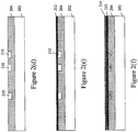
- a graphene layer 214 is formed on the gate dielectric layer 212.
- the transfer of graphene films may be performed in any suitable manner known in the art such as, for example, by a dry thermal release tape method.
- the graphene layer 214 is a monolayer of graphene.
- the gate electrodes have been labeled with "GN” and "GP" designations to indicated exemplary n-type and p-type FET devices.
- the graphene layer is patterned in accordance with the desired active areas, and corresponding to the location of the bottom orientation gate electrodes.
- the blanket gate dielectric layer 212 remains intact at this point.
- source/drain contacts 216 for the graphene based FET devices are formed, followed by gate dielectric layer patterning and formation of conductive pads 218 as illustrated in Figure 2(i) .
- an insulating layer 220 e.g., an oxide
- Vias 222 are then etched into the insulating layer 220 so as to provide vertical electrical connection to one or more additional levels of graphene based active devices, in accordance with a 3D IC structure.
- a second level 224 of graphene based active devices is shown connected to the first level of graphene based active devices.
- the second level 224 comprises FET devices with bottom orientation gates.
- a graphene based 3D IC structure could have both top orientation and bottom orientation gates in the same or different levels of the device.
Landscapes
- Thin Film Transistor (AREA)
- Metal-Oxide And Bipolar Metal-Oxide Semiconductor Integrated Circuits (AREA)
- Carbon And Carbon Compounds (AREA)
Description
- The present invention relates generally to semiconductor device manufacturing and, more particularly, to a graphene based, three-dimensional (3D) integrated circuit device.
- Graphene refers to a two-dimensional planar sheet of carbon atoms arranged in a hexagonal benzene-ring structure. A free-standing graphene structure is theoretically stable only in a two-dimensional space, which implies that a truly planar graphene structure does not exist in a three-dimensional space, being unstable with respect to formation of curved structures such as soot, fullerenes, nanotubes or buckled two dimensional structures. However, a two-dimensional graphene structure may be stable when supported on a substrate, for example, on the surface of a silicon carbide (SiC) crystal. Free standing graphene films have also been produced, but they may not have the idealized flat geometry.
- Structurally, graphene has hybrid orbitals formed by sp2 hybridization. In the sp2 hybridization, the 2s orbital and two of the three 2p orbitals mix to form three sp2 orbitals. The one remaining p-orbital forms a pi (π)-bond between the carbon atoms. Similar to the structure of benzene, the structure of graphene has a conjugated ring of the p-orbitals, i.e., the graphene structure is aromatic. Unlike other allotropes of carbon such as diamond, amorphous carbon, carbon nanofoam, or fullerenes, graphene is only one atomic layer thin.
- Graphene has an unusual band structure in which conical electron and hole pockets meet only at the K-points of the Brillouin zone in momentum space. The energy of the charge carriers, i.e., electrons or holes, has a linear dependence on the momentum of the carriers. As a consequence, the carriers behave as relativistic Dirac-Fermions with a zero effective mass and are governed by Dirac's equation. Graphene sheets may have a large carrier mobility of greater than 200,000 cm2/V-sec at 4K. Even at 300K, the carrier mobility can be as high as 15,000 cm2/V-sec.
- Graphene layers may be grown by solid-state graphitization, i.e., by sublimating silicon atoms from a surface of a silicon carbide crystal, such as the (0001) surface. At about 1,150°C, a complex pattern of surface reconstruction begins to appear at an initial stage of graphitization. Typically, a higher temperature is needed to form a graphene layer. Graphene layers on another material are also known in the art. For example, single or several layers of graphene maybe formed on a metal surface, such as copper and nickel, by chemical deposition of carbon atoms from a carbon-rich precursor.
- Graphene displays many other advantageous electrical properties such as electronic coherence at near room temperature and quantum interference effects. Ballistic transport properties in small scale structures are also expected in graphene layers.
- Despite the fact that the graphene was isolated for the first time only a few years ago (by using ordinary Scotch tape), this field currently being intensively studied. Because of the unique electrical properties such as those described above (e.g., high charge carrier mobility etc.), graphene is ultimately promising for electronic applications. For example, graphene transistors have been demonstrated recently, and more advanced graphene circuits arc considered to be promising candidates to perhaps replace silicon in future integrated circuit technology. In J. Meindl et al.: "Nanoelectronics in Retrospect, Prospect and Principle", ISSCC 2010, pages 31-35, it is reported that graphene demonstrated capability to serve as the source, channel and drain regions of a field effect transistor and as an interconnect. According to this document, using graphene, it would be possible to create a technology with no distinction between device and interconnection layers. Each chip would have multiple layers, where each layer could contain both devices, as well as interconnects, thereby reducing wire lengths and creating more optimal architectures. However, the lack of easy and low cost graphene fabrication processes presently limits the development of graphene applications.
- According to one aspect of the invention, there is provided a three-dimensional integrated circuit structure according to claim 1.
- According to another aspect of the invention, there is provided, a method of forming a three-dimensional (3D) integrated circuit (IC) structure according to claim 2.
- Referring to the exemplary drawings wherein like elements are numbered alike in the several Figures:
-
Figures 1(a) through 1(h) are a series of cross-sectional views illustrating a method of forming a graphene based, three-dimensional (3D) integrated circuit not forming part of the claimed invention; and -
Figures 2(a) through 2(k) are a series of cross-sectional views illustrating an exemplary method of forming a graphene based, 3D integrated circuit, in accordance with the invention. - Disclosed herein are graphene based, three-dimensional (3D) integrated circuit devices, and methods of forming the same. In the semiconductor industry, a 3D integrated circuit (1C) generally refers to a chip having two or more layers of active electronic components, integrated both vertically and horizontally into a single circuit. 3D ICs potentially offer many significant benefits, such as for example: a smaller footprint (more functionality fitting into a small space), speed (the average wire length becomes much shorter, in turn reducing signal propagation delay and increasing overall performance), power consumption (by keeping a signal on-chip, the resulting shorter wires reduce power consumption and produce less parasitic capacitance), and heterogeneous integration, to name a few. In the case of heterogeneous integration, different circuit layers may be formed with different processes, or even on different types of wafers. Moreover, components otherwise having completely incompatible manufacturing processes could be combined in a single device.
- Currently, 3D ICs may be formed by techniques such as wafer-on-wafer bonding, wherein electronic components are built on two or more semiconductor wafers, which are then aligned, bonded, and diced into 3D ICs. Each wafer may be thinned before or after bonding. Vertical connections are either built into the wafers before bonding or otherwise created in the stack after bonding. These "through-silicon vias" (TSVs) pass through the silicon substrate(s) between active layers and/or between an active layer and an external bond pad. In a die-on-wafer process, electronic components are built on two semiconductor wafers. One wafer is diced, and the singulated dies are aligned and bonded onto die sites of the second wafer. As in the wafer-on-wafer method, thinning and TSV creation are performed either before or after bonding. Additional dies may be added to the stacks before dicing. Alternatively, in a die-on-die process, electronic components are built on multiple dies, which are then aligned and bonded. Thinning and TSV creation may be done before or after bonding.
- In order to avoid multiple substrates and aligning, thinning, bonding, or TSV techniques, 3D ICs would desirably be formed monolithically. That is, the electronic components and their connections (wiring) are built in layers on a single semiconductor wafer, which is then diced into 3D ICs. Unfortunately, existing applications of this method are currently limited because creating conventional transistors in semiconductor layers (e.g., dopant implantation and activation annealing) requires processing temperatures that are sufficient any existing wiring.
- Accordingly,
Figures 1(a) through 1(h) are a series of cross-sectional views illustrating a method of forming a graphene based, three-dimensional (3D) integrated circuit. Beginning inFigure 1(a) , a starting substrate 102 (e.g., silicon) has an insulating layer (e.g., an oxide such as SiO2) 104 formed thereon. InFigure 1(b) , ablanket graphene layer 106 is transferred onto theinsulating layer 104. The transfer of graphene films may be performed in any suitable manner known in the art such as, for example, by a dry thermal release tape process. Notably, because graphene is deposited on such a substrate surface in this manner, it is a particularly suitable material for 3D integration. - As shown in
Figure 1(c) , thegraphene layer 106 is patterned through appropriate lithography techniques (e.g., hardmask and/or photoresist layer formation, development and etching) to form desired active areas of graphene-based devices. This is followed by a first level of transistor device formation. As shown inFigure 1(d) , the grapheneactive areas 106 are covered with transistor gate stack materials such as, for example, a gatedielectric layer 108 and agate electrode layer 110. The gatedielectric layer 108 may be a high-k material such as hafnium, hafnium silicate, zirconium oxide, zirconium silicate, nitrided dielectrics, as well as combinations thereof. Thegate electrode layer 110 may include polysilicon, a metal, or combinations thereof. - Referring now to
Figure 1(e) , the gate dielectric and gate electrode layers 108, 110 are then patterned so as to define transistor devices (e.g., field effect transistors or FETs) on the patterned grapheneactive areas 106, includinggate electrodes 112 and gate dielectric layers 114. It should be noted that the patterning operation depicted in the figures is only illustrative in nature, in that more than one patterning and RIE process may be used, for example, in accordance with different gate stack requirements depending on the type and polarity of the transistor device. Thus, in the example shown, the designation "GN" refers to a transistor gate for an n-type device (e.g., an NFET) while the designation "GP" refers to a transistor gate for a p-type device (e.g., a PFET). - Following gate stack patterning, the formation of source/
drain contacts 116 andconductive pad structures 118 is shown inFigure 1(f) . The formation of the source and drain contacts includes, for example deposition of source/drain contact material and patterning. The source/drain contact material may be a metal material such as, for example, titanium (Ti), palladium (Pd), aluminum (Al), tungsten (W), or alloys thereof. The deposition method can be may include, for example, sputtering, and atomic layer deposition (ALD). - Upon completion of a first layer of graphene circuit devices, an insulating layer 120 (e.g., an oxide) is formed over the devices as shown in
Figure 1(g) .Vias 122 are then etched into the insulatinglayer 120 so as to provide vertical electrical connection to one or more additional levels of graphene based active devices, in accordance with a 3D IC structure. InFigure 1(h) , thelower level 124 of graphene based active devices is shown connected to anupper layer 126 of graphene based active devices. The formation of theupper level 126 is similar to that of thelower level 124, in that a graphene layer (e.g., monolayer) is first deposited/transferred onto the completedlower level 124, followed by pattering of the desired active areas of the graphene, formation and patterning of the gate stack materials, formation and patterning of the source/drain contacts and conductive pads, and formation of an insulating layer over the upper level devices. - Although the example depicts a pair of graphene based active device levels, it will be appreciated that the above process may be repeated as desired to form still additional graphene based active device levels. In one contemplated example, each level of graphene may have different functions (e.g., logic, analog, memory).
- The 3D IC device shown in the process flow sequence of
Figures 1(a) through 1(h) is an example of a top gate orientation, in that the gate electrode and dielectric are disposed above the active graphene source/drain regions. However, according to the invention the active graphene devices are formed using a bottom orientation, as depicted in the process flow sequence ofFigures 2(a) through 2(k) . Beginning inFigure 2(a) , a starting substrate 202 (e.g., silicon) has an insulating layer (e.g., an oxide such as SiO2) 204 formed thereon, similar to the top gate orientation process ofFigure 1(a) . - Rather than transferring a graphene layer to the insulating
layer 204 at this point in the process, the insulatinglayer 204 is instead patterned withvias 206 corresponding to the locations of the gates of the lower level graphene based devices, as shown inFigure 2(b) . Then, as shown inFigure 2(c) , agate electrode layer 208 is formed over the device, filling in the vias. Once thegate electrode layer 208 is planarized,individual gate electrodes 210 are now defined, as shown inFigure 2(d) . Agate dielectric layer 212 is then formed over the insulatinglayer 204 andgate electrodes 210, as shown inFigure 2(e) . Thegate dielectric layer 212 may be a high-k gate dielectric layer. - Referring now to
Figure 2(f) , agraphene layer 214 is formed on thegate dielectric layer 212. Again, the transfer of graphene films may be performed in any suitable manner known in the art such as, for example, by a dry thermal release tape method. In one exemplary embodiment, thegraphene layer 214 is a monolayer of graphene. As also shown inFigure 2(f) , the gate electrodes have been labeled with "GN" and "GP" designations to indicated exemplary n-type and p-type FET devices. - In
Figure 2(g) , the graphene layer is patterned in accordance with the desired active areas, and corresponding to the location of the bottom orientation gate electrodes. The blanketgate dielectric layer 212 remains intact at this point. As then shown inFigure 2(h) , source/drain contacts 216 for the graphene based FET devices are formed, followed by gate dielectric layer patterning and formation ofconductive pads 218 as illustrated inFigure 2(i) . Thus configured, a first or lower layer of graphene based active devices is completed, and followed by the formation of an insulating layer 220 (e.g., an oxide) over the devices as shown inFigure 2(j) .Vias 222 are then etched into the insulatinglayer 220 so as to provide vertical electrical connection to one or more additional levels of graphene based active devices, in accordance with a 3D IC structure. Finally, inFigure 2(k) , asecond level 224 of graphene based active devices is shown connected to the first level of graphene based active devices. According to the invention, also thesecond level 224 comprises FET devices with bottom orientation gates. However, it is still further contemplated that a graphene based 3D IC structure could have both top orientation and bottom orientation gates in the same or different levels of the device. - While the invention has been described with reference to a preferred embodiment or embodiments, it will be understood by those skilled in the art that various changes may be made and equivalents may be substituted for elements thereof without departing from the scope of the invention. In addition, many modifications may be made to adapt a particular situation or material to the teachings of the invention without departing from the scope thereof. Therefore, it is intended that the invention not be limited to the particular embodiment disclosed as the best mode contemplated for carrying out this invention, but that the invention will include all embodiments falling within the scope of the appended claims.
Claims (2)
- A three-dimensional integrated circuit structure, comprising:a first insulating layer (204) formed over a substrate (202);first gate electrodes (GN, GP) formed in openings in the first dielectric layer (204);a first gate dielectric layer (212) formed over the first insulating layer (204) and the first gate electrodes (GN, GP);a first layer of graphene (214) formed over the first gate dielectric layer (212);a first level of one or more field effect transistors having gate structures respectively comprising the first gate electrodes (GN, GP) and the first gate dielectric layer (212) in contact with the first layer of graphene (214);a second insulating layer (220) formed over the first level of one or more field effect transistors;second gate electrodes (GN, GP) formed in openings in the second dielectric layer (220);a second gate dielectric layer formed over the second insulating layer (220) and the second gate electrodes (GN, GP);a second layer of graphene (224) formed over the second gate dielectric layer; anda second level of one or more field effect transistors having gate structures respectively comprising the second gate electrodes (GN, GP) and the second gate dielectric layer in contact with the second layer of graphene (224), the second level of one or more field effect transistors electrically interconnected with the first level of one or more field effect transistors, wherein the one or more field effect transistors of the first and second levels have a bottom gate orientation relationship with respect to the associated graphene layer (214, 224);a plurality of source and drain contacts (216) disposed on each of the first and second layers of graphene (214, 224), above the first and second gate electrodes (GN, GP) under the graphene layers (214, 224);one or more first level conductive pad structures (218) formed adjacent the first layer of graphene (214) such that a bottom surface of the one or more first level conductive pad structures (218) is substantially co-planar with a bottom surface of the first gate dielectric layer (212); andone or more second level conductive pad structures (218) formed adjacent the second layer of graphene (224) such that a bottom surface of the one or more second level conductive pad structures (218) is substantially co-planar with a bottom surface of the second gate dielectric layer;wherein the graphene is a two-dimensional planar sheet of carbon atoms arranged in a hexagonal benzene ring structure.
- A method of forming a three-dimensional integrated circuit structure, the method comprising:forming a first insulating layer (204) over a substrate (202) forming a first layer of graphene (214) over the first insulating layer (204);forming a first level of one or more field effect transistors having gate structures in contact with the first layer of graphene (214);forming a second insulating layer (220) over the first level of one or more field effect transistors;forming a second layer of graphene (224) over the second insulating layer (220); andforming a second level of one or more field effect transistors having gate structures in contact with the second layer of graphene (224), the second level of one or more field effect transistors electrically interconnected with the first level of one or more field effect transistors, wherein the one or more field effect transistors of the first and second levels have a bottom gate orientation relationship with respect to the associated graphene layer (214, 224), and wherein the one or more field effect transistors of each of the first and second levels are respectively formed by the following steps in sequence:forming openings in the associated insulating layer (204, 220) in accordance with a desired gate pattern;filling the openings in the associated insulating layer (204, 220) with a gate electrode material and planarizing the gate electrode material to form individual gate electrodes (GN, GP);forming a gate dielectric layer (212) over the individual gate electrodes (GN, GP);forming the associated graphene layer (214, 224) over the gate dielectric layer; andpatterning the associated graphene layer (214, 224) in accordance with a desired active area;forming a plurality of source and drain contacts (216) disposed on the graphene layers (214, 224), above the individual gate electrodes (GN, GP) under the graphene layers; andpatterning the gate dielectric layer, wherein the individual gate electrodes and the gate dielectric layer constitute said gate structures;wherein the method of forming a three-dimensional integrated circuit structure further comprises, after formation of the one or more field effect transistors of the respective level:forming one or more first level conductive pad structures (218) adjacent the first layer of graphene (214) such that a bottom surface of the one or more first level conductive pad structures (218) is substantially co-planar with a bottom surface of the first gate dielectric layer (212); andforming one or more second level conductive pad structures (218) adjacent the second layer of graphene (224) such that a bottom surface of the one or more second level conductive pad structures (218) is substantially co-planar with a bottom surface of the second gate dielectric layer;wherein the graphene is a two-dimensional planar sheet of carbon atoms arranged in a hexagonal benzene ring structure.
Applications Claiming Priority (2)
| Application Number | Priority Date | Filing Date | Title |
|---|---|---|---|
| US12/719,058 US8450779B2 (en) | 2010-03-08 | 2010-03-08 | Graphene based three-dimensional integrated circuit device |
| PCT/US2011/023665 WO2011112300A1 (en) | 2010-03-08 | 2011-02-04 | Graphene based three-dimensional integrated circuit device |
Publications (3)
| Publication Number | Publication Date |
|---|---|
| EP2545586A1 EP2545586A1 (en) | 2013-01-16 |
| EP2545586A4 EP2545586A4 (en) | 2016-03-30 |
| EP2545586B1 true EP2545586B1 (en) | 2020-06-10 |
Family
ID=44530512
Family Applications (1)
| Application Number | Title | Priority Date | Filing Date |
|---|---|---|---|
| EP11753755.5A Active EP2545586B1 (en) | 2010-03-08 | 2011-02-04 | Graphene based three-dimensional integrated circuit device |
Country Status (7)
| Country | Link |
|---|---|
| US (2) | US8450779B2 (en) |
| EP (1) | EP2545586B1 (en) |
| JP (1) | JP5870046B2 (en) |
| CN (1) | CN102782856B (en) |
| CA (1) | CA2787094A1 (en) |
| TW (1) | TWI525775B (en) |
| WO (1) | WO2011112300A1 (en) |
Families Citing this family (45)
| Publication number | Priority date | Publication date | Assignee | Title |
|---|---|---|---|---|
| US8421082B1 (en) * | 2010-01-19 | 2013-04-16 | Mcube, Inc. | Integrated CMOS and MEMS with air dielectric method and system |
| KR20110098441A (en) * | 2010-02-26 | 2011-09-01 | 삼성전자주식회사 | Graphene Electronic Device and Manufacturing Method |
| US9024300B2 (en) * | 2010-05-13 | 2015-05-05 | Nokia Corporation | Manufacture of graphene-based apparatus |
| JP5664119B2 (en) * | 2010-10-25 | 2015-02-04 | ソニー株式会社 | Transparent conductive film, method for manufacturing transparent conductive film, photoelectric conversion device, and electronic device |
| KR20120063164A (en) | 2010-12-07 | 2012-06-15 | 삼성전자주식회사 | Graphene structure and method of fabricating the same |
| US8748871B2 (en) | 2011-01-19 | 2014-06-10 | International Business Machines Corporation | Graphene devices and semiconductor field effect transistors in 3D hybrid integrated circuits |
| US8409957B2 (en) | 2011-01-19 | 2013-04-02 | International Business Machines Corporation | Graphene devices and silicon field effect transistors in 3D hybrid integrated circuits |
| WO2013052679A1 (en) * | 2011-10-04 | 2013-04-11 | Qualcomm Incorporated | Monolithic 3-d integration using graphene |
| FR2985371A1 (en) * | 2011-12-29 | 2013-07-05 | Commissariat Energie Atomique | METHOD FOR MANUFACTURING A MULTILAYER STRUCTURE ON A SUPPORT |
| KR101349817B1 (en) * | 2012-02-08 | 2014-01-10 | 한국화학연구원 | Graphene touch panel using pattern graphene and manufacture method thereof |
| US8680511B2 (en) * | 2012-02-09 | 2014-03-25 | International Business Machines Corporation | Bilayer gate dielectric with low equivalent oxide thickness for graphene devices |
| JP5910294B2 (en) * | 2012-05-10 | 2016-04-27 | 富士通株式会社 | Electronic device and manufacturing method of laminated structure |
| US8519450B1 (en) | 2012-08-17 | 2013-08-27 | International Business Machines Corporation | Graphene-based non-volatile memory |
| US9098666B2 (en) | 2012-11-28 | 2015-08-04 | Qualcomm Incorporated | Clock distribution network for 3D integrated circuit |
| US9064077B2 (en) | 2012-11-28 | 2015-06-23 | Qualcomm Incorporated | 3D floorplanning using 2D and 3D blocks |
| US9536840B2 (en) * | 2013-02-12 | 2017-01-03 | Qualcomm Incorporated | Three-dimensional (3-D) integrated circuits (3DICS) with graphene shield, and related components and methods |
| US9041448B2 (en) | 2013-03-05 | 2015-05-26 | Qualcomm Incorporated | Flip-flops in a monolithic three-dimensional (3D) integrated circuit (IC) (3DIC) and related methods |
| US9177890B2 (en) | 2013-03-07 | 2015-11-03 | Qualcomm Incorporated | Monolithic three dimensional integration of semiconductor integrated circuits |
| US9171608B2 (en) | 2013-03-15 | 2015-10-27 | Qualcomm Incorporated | Three-dimensional (3D) memory cell separation among 3D integrated circuit (IC) tiers, and related 3D integrated circuits (3DICS), 3DIC processor cores, and methods |
| WO2014150584A1 (en) * | 2013-03-15 | 2014-09-25 | Solan, Llc. | Functional inclusion of interlayer devices in multi-level graphene devices and methods for forming same |
| KR102059131B1 (en) * | 2013-04-05 | 2019-12-24 | 삼성전자주식회사 | Graphene device, and method of fabricating the same |
| US9418985B2 (en) | 2013-07-16 | 2016-08-16 | Qualcomm Incorporated | Complete system-on-chip (SOC) using monolithic three dimensional (3D) integrated circuit (IC) (3DIC) technology |
| US9411922B2 (en) | 2013-08-15 | 2016-08-09 | Empire Technology Development Llc | Yield optimization of processor with graphene-based transistors |
| CN105830046A (en) | 2013-08-15 | 2016-08-03 | 英派尔科技开发有限公司 | Heterogeneous multi-core processor with graphene-based transistors |
| US9240478B2 (en) | 2014-04-16 | 2016-01-19 | Taiwan Semiconductor Manufacturing Company, Ltd. | 3D UTB transistor using 2D material channels |
| US9812604B2 (en) * | 2014-05-30 | 2017-11-07 | Klaus Y. J. Hsu | Photosensing device with graphene |
| US10050104B2 (en) * | 2014-08-20 | 2018-08-14 | Taiwan Semiconductor Manufacturing Company, Ltd. | Capacitor having a graphene structure, semiconductor device including the capacitor and method of forming the same |
| JP2016058449A (en) * | 2014-09-05 | 2016-04-21 | 住友電気工業株式会社 | Semiconductor device |
| US10020300B2 (en) | 2014-12-18 | 2018-07-10 | Agilome, Inc. | Graphene FET devices, systems, and methods of using the same for sequencing nucleic acids |
| US9857328B2 (en) | 2014-12-18 | 2018-01-02 | Agilome, Inc. | Chemically-sensitive field effect transistors, systems and methods for manufacturing and using the same |
| US9618474B2 (en) | 2014-12-18 | 2017-04-11 | Edico Genome, Inc. | Graphene FET devices, systems, and methods of using the same for sequencing nucleic acids |
| US10429342B2 (en) | 2014-12-18 | 2019-10-01 | Edico Genome Corporation | Chemically-sensitive field effect transistor |
| US10006910B2 (en) | 2014-12-18 | 2018-06-26 | Agilome, Inc. | Chemically-sensitive field effect transistors, systems, and methods for manufacturing and using the same |
| US9859394B2 (en) | 2014-12-18 | 2018-01-02 | Agilome, Inc. | Graphene FET devices, systems, and methods of using the same for sequencing nucleic acids |
| US9987830B2 (en) * | 2015-08-18 | 2018-06-05 | Infineon Technologies Ag | Method for processing a carrier and method for transferring a graphene layer |
| WO2017044577A1 (en) * | 2015-09-08 | 2017-03-16 | Massachusetts Institute Of Technology | Systems and methods for graphene based layer transfer |
| US9640430B2 (en) * | 2015-09-17 | 2017-05-02 | Nxp Usa, Inc. | Semiconductor device with graphene encapsulated metal and method therefor |
| EP3459115A4 (en) | 2016-05-16 | 2020-04-08 | Agilome, Inc. | GRAPHEN-FET DEVICES, SYSTEMS AND METHODS FOR USE THEREOF FOR SEQUENCING NUCLEIC ACIDS |
| JP6791723B2 (en) * | 2016-11-07 | 2020-11-25 | 住友電気工業株式会社 | Semiconductor device |
| CN109712961B (en) * | 2017-10-25 | 2021-11-02 | 上海新微技术研发中心有限公司 | Three-dimensional integrated circuit and method of manufacturing the same |
| FR3073977B1 (en) | 2017-11-22 | 2021-12-03 | Commissariat Energie Atomique | RETURNED GRID 3D CIRCUIT TRANSISTORS |
| JP2021527618A (en) | 2018-06-22 | 2021-10-14 | マサチューセッツ インスティテュート オブ テクノロジー | Systems and methods for the growth of silicon carbide on layers with graphene and / or hexagonal boron nitride and related articles. |
| CN111430354A (en) * | 2020-03-12 | 2020-07-17 | 复旦大学 | Low-power-consumption semi-floating gate memory and preparation method thereof |
| US11424198B2 (en) * | 2020-09-01 | 2022-08-23 | Nanya Technology Corporation | Semiconductor device with graphene layers and method for fabricating the same |
| US11854933B2 (en) * | 2020-12-30 | 2023-12-26 | Texas Instruments Incorporated | Thermally conductive wafer layer |
Family Cites Families (33)
| Publication number | Priority date | Publication date | Assignee | Title |
|---|---|---|---|---|
| US6271542B1 (en) * | 1997-12-08 | 2001-08-07 | International Business Machines Corporation | Merged logic and memory combining thin film and bulk Si transistors |
| JP2000327317A (en) * | 1999-05-20 | 2000-11-28 | Ise Electronics Corp | Graphite nano-fiber, its production and production apparatus |
| US7297977B2 (en) * | 2004-03-12 | 2007-11-20 | Hewlett-Packard Development Company, L.P. | Semiconductor device |
| JP2005285822A (en) * | 2004-03-26 | 2005-10-13 | Fujitsu Ltd | Semiconductor device and semiconductor sensor |
| US7312487B2 (en) * | 2004-08-16 | 2007-12-25 | International Business Machines Corporation | Three dimensional integrated circuit |
| US7141727B1 (en) * | 2005-05-16 | 2006-11-28 | International Business Machines Corporation | Method and apparatus for fabricating a carbon nanotube transistor having unipolar characteristics |
| KR100704919B1 (en) | 2005-10-14 | 2007-04-09 | 삼성전기주식회사 | Substrate without core layer and its manufacturing method |
| JP2007123377A (en) * | 2005-10-26 | 2007-05-17 | Matsushita Electric Ind Co Ltd | Organic semiconductor element module |
| US7514710B2 (en) * | 2005-12-28 | 2009-04-07 | 3M Innovative Properties Company | Bottom gate thin film transistors |
| US7619257B2 (en) | 2006-02-16 | 2009-11-17 | Alcatel-Lucent Usa Inc. | Devices including graphene layers epitaxially grown on single crystal substrates |
| US7391109B2 (en) | 2006-05-22 | 2008-06-24 | Hewlett-Packard Development Company, L.P. | Integrated circuit interconnect |
| JP5167479B2 (en) | 2006-06-13 | 2013-03-21 | 国立大学法人北海道大学 | Method for manufacturing graphene integrated circuit |
| MY149475A (en) * | 2006-09-06 | 2013-08-30 | Univ Illinois | Controlled buckling structures in semiconductor interconnects and nanomembranes for stretchable electronics |
| US7858918B2 (en) | 2007-02-05 | 2010-12-28 | Ludwig Lester F | Molecular transistor circuits compatible with carbon nanotube sensors and transducers |
| US7838809B2 (en) | 2007-02-17 | 2010-11-23 | Ludwig Lester F | Nanoelectronic differential amplifiers and related circuits having carbon nanotubes, graphene nanoribbons, or other related materials |
| US7732859B2 (en) | 2007-07-16 | 2010-06-08 | International Business Machines Corporation | Graphene-based transistor |
| WO2009015287A2 (en) | 2007-07-25 | 2009-01-29 | California Institute Of Technology | Functional anchors connecting graphene-like carbon to metal |
| US20090174435A1 (en) | 2007-10-01 | 2009-07-09 | University Of Virginia | Monolithically-Integrated Graphene-Nano-Ribbon (GNR) Devices, Interconnects and Circuits |
| US8043978B2 (en) * | 2007-10-11 | 2011-10-25 | Riken | Electronic device and method for producing electronic device |
| US8659009B2 (en) | 2007-11-02 | 2014-02-25 | The Trustees Of Columbia University In The City Of New York | Locally gated graphene nanostructures and methods of making and using |
| JP5109648B2 (en) * | 2007-12-27 | 2012-12-26 | 富士通株式会社 | Method for manufacturing layered carbon structure and method for manufacturing semiconductor device |
| US7772059B2 (en) | 2008-01-16 | 2010-08-10 | Texas Instruments Incorporated | Method for fabricating graphene transistors on a silicon or SOI substrate |
| FI20085113A0 (en) | 2008-02-08 | 2008-02-08 | Valtion Teknillinen | Process for manufacturing graphene structures on substrates |
| US7948042B2 (en) | 2008-03-03 | 2011-05-24 | The Regents Of The University Of California | Suspended structures |
| JP5202046B2 (en) * | 2008-03-13 | 2013-06-05 | 株式会社半導体エネルギー研究所 | Semiconductor device and manufacturing method of semiconductor device |
| US8133793B2 (en) | 2008-05-16 | 2012-03-13 | Sandisk 3D Llc | Carbon nano-film reversible resistance-switchable elements and methods of forming the same |
| KR101490111B1 (en) * | 2008-05-29 | 2015-02-06 | 삼성전자주식회사 | An epitaxial graphene, a method of forming the stacked structure, and an electronic device including the stacked structure |
| US8716805B2 (en) * | 2008-06-10 | 2014-05-06 | Toshiba America Research, Inc. | CMOS integrated circuits with bonded layers containing functional electronic devices |
| US7952088B2 (en) * | 2008-07-11 | 2011-05-31 | International Business Machines Corporation | Semiconducting device having graphene channel |
| US7858990B2 (en) * | 2008-08-29 | 2010-12-28 | Advanced Micro Devices, Inc. | Device and process of forming device with pre-patterned trench and graphene-based device structure formed therein |
| KR101156620B1 (en) * | 2009-04-08 | 2012-06-14 | 한국전자통신연구원 | Field effect transistor having graphene channel layer |
| WO2011031949A1 (en) * | 2009-09-10 | 2011-03-17 | Lockheed Martin Corporation | Graphene nanoelectronic device fabrication |
| US8124463B2 (en) * | 2009-09-21 | 2012-02-28 | International Business Machines Corporation | Local bottom gates for graphene and carbon nanotube devices |
-
2010
- 2010-03-08 US US12/719,058 patent/US8450779B2/en active Active
-
2011
- 2011-02-04 CN CN201180011564.XA patent/CN102782856B/en active Active
- 2011-02-04 CA CA2787094A patent/CA2787094A1/en not_active Abandoned
- 2011-02-04 JP JP2012557052A patent/JP5870046B2/en not_active Expired - Fee Related
- 2011-02-04 WO PCT/US2011/023665 patent/WO2011112300A1/en not_active Ceased
- 2011-02-04 EP EP11753755.5A patent/EP2545586B1/en active Active
- 2011-03-01 TW TW100106730A patent/TWI525775B/en not_active IP Right Cessation
-
2012
- 2012-07-25 US US13/557,501 patent/US8895372B2/en active Active
Non-Patent Citations (1)
| Title |
|---|
| None * |
Also Published As
| Publication number | Publication date |
|---|---|
| JP2013522873A (en) | 2013-06-13 |
| US8895372B2 (en) | 2014-11-25 |
| EP2545586A1 (en) | 2013-01-16 |
| CN102782856B (en) | 2015-11-25 |
| EP2545586A4 (en) | 2016-03-30 |
| US20120295423A1 (en) | 2012-11-22 |
| WO2011112300A1 (en) | 2011-09-15 |
| TWI525775B (en) | 2016-03-11 |
| JP5870046B2 (en) | 2016-02-24 |
| CA2787094A1 (en) | 2011-09-15 |
| CN102782856A (en) | 2012-11-14 |
| US20110215300A1 (en) | 2011-09-08 |
| TW201201340A (en) | 2012-01-01 |
| US8450779B2 (en) | 2013-05-28 |
Similar Documents
| Publication | Publication Date | Title |
|---|---|---|
| US8895372B2 (en) | Graphene based three-dimensional integrated circuit device | |
| TWI854086B (en) | 3d complementary metal oxide semiconductor (cmos) device and method of forming the same | |
| TWI741935B (en) | Semiconductor devices and method of forming the same | |
| TW202143335A (en) | Packaged semiconductor devices and methods of forming the same | |
| US11302695B2 (en) | Method for forming integrated semiconductor device with 2D material layer | |
| TW202127670A (en) | High performance nanosheet fabrication method with enhanced high mobility channel elements | |
| TW202101733A (en) | Self-aligned gate endcap (sage) architecture having gate or contact plugs | |
| KR102787383B1 (en) | Staggered stacked vertical crystalline semiconducting channels | |
| JP7799043B2 (en) | How to ultra-thin wafers | |
| TW202101768A (en) | Self-aligned gate endcap (sage) architecture having gate contacts | |
| US11158807B2 (en) | Field effect transistor and method of manufacturing the same | |
| US20250089317A1 (en) | Nanosheet structures with bottom semiconductor material | |
| TW202418549A (en) | Isolation rail between backside power rails | |
| US20250343089A1 (en) | Heat dissipation in semiconductor devices | |
| US20250072049A1 (en) | Semiconductor device isolation of contact and source/drain structures | |
| US20250142901A1 (en) | Semiconductor devices with embedded backside capacitors | |
| US20250006687A1 (en) | Heat dissipation in semiconductor devices | |
| TW202539449A (en) | Semiconductor devices, semiconductor structures, and methods of manufacturing the same |
Legal Events
| Date | Code | Title | Description |
|---|---|---|---|
| PUAI | Public reference made under article 153(3) epc to a published international application that has entered the european phase |
Free format text: ORIGINAL CODE: 0009012 |
|
| 17P | Request for examination filed |
Effective date: 20121004 |
|
| AK | Designated contracting states |
Kind code of ref document: A1 Designated state(s): AL AT BE BG CH CY CZ DE DK EE ES FI FR GB GR HR HU IE IS IT LI LT LU LV MC MK MT NL NO PL PT RO RS SE SI SK SM TR |
|
| DAX | Request for extension of the european patent (deleted) | ||
| RA4 | Supplementary search report drawn up and despatched (corrected) |
Effective date: 20160301 |
|
| RIC1 | Information provided on ipc code assigned before grant |
Ipc: H01L 27/06 20060101AFI20160224BHEP Ipc: H01L 29/16 20060101ALN20160224BHEP |
|
| RIN1 | Information on inventor provided before grant (corrected) |
Inventor name: LIN, CHUNG-HSUN Inventor name: HEN, SHU-JEN Inventor name: SU, NING Inventor name: GUO, DECHAO |
|
| STAA | Information on the status of an ep patent application or granted ep patent |
Free format text: STATUS: EXAMINATION IS IN PROGRESS |
|
| 17Q | First examination report despatched |
Effective date: 20190418 |
|
| REG | Reference to a national code |
Ref country code: DE Ref legal event code: R079 Ref document number: 602011067249 Country of ref document: DE Free format text: PREVIOUS MAIN CLASS: H01L0029120000 Ipc: H01L0027060000 |
|
| RIC1 | Information provided on ipc code assigned before grant |
Ipc: H01L 27/088 20060101ALI20191205BHEP Ipc: H01L 27/06 20060101AFI20191205BHEP Ipc: H01L 21/8256 20060101ALI20191205BHEP Ipc: H01L 29/16 20060101ALN20191205BHEP |
|
| GRAP | Despatch of communication of intention to grant a patent |
Free format text: ORIGINAL CODE: EPIDOSNIGR1 |
|
| STAA | Information on the status of an ep patent application or granted ep patent |
Free format text: STATUS: GRANT OF PATENT IS INTENDED |
|
| INTG | Intention to grant announced |
Effective date: 20200127 |
|
| RAP1 | Party data changed (applicant data changed or rights of an application transferred) |
Owner name: GLOBALFOUNDRIES INC. |
|
| GRAS | Grant fee paid |
Free format text: ORIGINAL CODE: EPIDOSNIGR3 |
|
| GRAA | (expected) grant |
Free format text: ORIGINAL CODE: 0009210 |
|
| STAA | Information on the status of an ep patent application or granted ep patent |
Free format text: STATUS: THE PATENT HAS BEEN GRANTED |
|
| AK | Designated contracting states |
Kind code of ref document: B1 Designated state(s): AL AT BE BG CH CY CZ DE DK EE ES FI FR GB GR HR HU IE IS IT LI LT LU LV MC MK MT NL NO PL PT RO RS SE SI SK SM TR |
|
| REG | Reference to a national code |
Ref country code: GB Ref legal event code: FG4D |
|
| REG | Reference to a national code |
Ref country code: AT Ref legal event code: REF Ref document number: 1279868 Country of ref document: AT Kind code of ref document: T Effective date: 20200615 Ref country code: CH Ref legal event code: EP |
|
| REG | Reference to a national code |
Ref country code: DE Ref legal event code: R096 Ref document number: 602011067249 Country of ref document: DE |
|
| REG | Reference to a national code |
Ref country code: IE Ref legal event code: FG4D |
|
| REG | Reference to a national code |
Ref country code: LT Ref legal event code: MG4D |
|
| PG25 | Lapsed in a contracting state [announced via postgrant information from national office to epo] |
Ref country code: LT Free format text: LAPSE BECAUSE OF FAILURE TO SUBMIT A TRANSLATION OF THE DESCRIPTION OR TO PAY THE FEE WITHIN THE PRESCRIBED TIME-LIMIT Effective date: 20200610 Ref country code: FI Free format text: LAPSE BECAUSE OF FAILURE TO SUBMIT A TRANSLATION OF THE DESCRIPTION OR TO PAY THE FEE WITHIN THE PRESCRIBED TIME-LIMIT Effective date: 20200610 Ref country code: SE Free format text: LAPSE BECAUSE OF FAILURE TO SUBMIT A TRANSLATION OF THE DESCRIPTION OR TO PAY THE FEE WITHIN THE PRESCRIBED TIME-LIMIT Effective date: 20200610 Ref country code: NO Free format text: LAPSE BECAUSE OF FAILURE TO SUBMIT A TRANSLATION OF THE DESCRIPTION OR TO PAY THE FEE WITHIN THE PRESCRIBED TIME-LIMIT Effective date: 20200910 Ref country code: GR Free format text: LAPSE BECAUSE OF FAILURE TO SUBMIT A TRANSLATION OF THE DESCRIPTION OR TO PAY THE FEE WITHIN THE PRESCRIBED TIME-LIMIT Effective date: 20200911 |
|
| REG | Reference to a national code |
Ref country code: NL Ref legal event code: MP Effective date: 20200610 |
|
| PG25 | Lapsed in a contracting state [announced via postgrant information from national office to epo] |
Ref country code: BG Free format text: LAPSE BECAUSE OF FAILURE TO SUBMIT A TRANSLATION OF THE DESCRIPTION OR TO PAY THE FEE WITHIN THE PRESCRIBED TIME-LIMIT Effective date: 20200910 Ref country code: LV Free format text: LAPSE BECAUSE OF FAILURE TO SUBMIT A TRANSLATION OF THE DESCRIPTION OR TO PAY THE FEE WITHIN THE PRESCRIBED TIME-LIMIT Effective date: 20200610 Ref country code: HR Free format text: LAPSE BECAUSE OF FAILURE TO SUBMIT A TRANSLATION OF THE DESCRIPTION OR TO PAY THE FEE WITHIN THE PRESCRIBED TIME-LIMIT Effective date: 20200610 Ref country code: RS Free format text: LAPSE BECAUSE OF FAILURE TO SUBMIT A TRANSLATION OF THE DESCRIPTION OR TO PAY THE FEE WITHIN THE PRESCRIBED TIME-LIMIT Effective date: 20200610 |
|
| REG | Reference to a national code |
Ref country code: AT Ref legal event code: MK05 Ref document number: 1279868 Country of ref document: AT Kind code of ref document: T Effective date: 20200610 |
|
| PG25 | Lapsed in a contracting state [announced via postgrant information from national office to epo] |
Ref country code: AL Free format text: LAPSE BECAUSE OF FAILURE TO SUBMIT A TRANSLATION OF THE DESCRIPTION OR TO PAY THE FEE WITHIN THE PRESCRIBED TIME-LIMIT Effective date: 20200610 Ref country code: NL Free format text: LAPSE BECAUSE OF FAILURE TO SUBMIT A TRANSLATION OF THE DESCRIPTION OR TO PAY THE FEE WITHIN THE PRESCRIBED TIME-LIMIT Effective date: 20200610 |
|
| REG | Reference to a national code |
Ref country code: DE Ref legal event code: R082 Ref document number: 602011067249 Country of ref document: DE Representative=s name: BOEHMERT & BOEHMERT ANWALTSPARTNERSCHAFT MBB -, DE Ref country code: DE Ref legal event code: R081 Ref document number: 602011067249 Country of ref document: DE Owner name: TAIWAN SEMICONDUCTOR MANUFACTURING COMPANY, LT, TW Free format text: FORMER OWNER: GLOBALFOUNDRIES INC., GRAND CAYMAN, KY |
|
| PG25 | Lapsed in a contracting state [announced via postgrant information from national office to epo] |
Ref country code: ES Free format text: LAPSE BECAUSE OF FAILURE TO SUBMIT A TRANSLATION OF THE DESCRIPTION OR TO PAY THE FEE WITHIN THE PRESCRIBED TIME-LIMIT Effective date: 20200610 Ref country code: RO Free format text: LAPSE BECAUSE OF FAILURE TO SUBMIT A TRANSLATION OF THE DESCRIPTION OR TO PAY THE FEE WITHIN THE PRESCRIBED TIME-LIMIT Effective date: 20200610 Ref country code: EE Free format text: LAPSE BECAUSE OF FAILURE TO SUBMIT A TRANSLATION OF THE DESCRIPTION OR TO PAY THE FEE WITHIN THE PRESCRIBED TIME-LIMIT Effective date: 20200610 Ref country code: SM Free format text: LAPSE BECAUSE OF FAILURE TO SUBMIT A TRANSLATION OF THE DESCRIPTION OR TO PAY THE FEE WITHIN THE PRESCRIBED TIME-LIMIT Effective date: 20200610 Ref country code: AT Free format text: LAPSE BECAUSE OF FAILURE TO SUBMIT A TRANSLATION OF THE DESCRIPTION OR TO PAY THE FEE WITHIN THE PRESCRIBED TIME-LIMIT Effective date: 20200610 Ref country code: IT Free format text: LAPSE BECAUSE OF FAILURE TO SUBMIT A TRANSLATION OF THE DESCRIPTION OR TO PAY THE FEE WITHIN THE PRESCRIBED TIME-LIMIT Effective date: 20200610 Ref country code: CZ Free format text: LAPSE BECAUSE OF FAILURE TO SUBMIT A TRANSLATION OF THE DESCRIPTION OR TO PAY THE FEE WITHIN THE PRESCRIBED TIME-LIMIT Effective date: 20200610 Ref country code: PT Free format text: LAPSE BECAUSE OF FAILURE TO SUBMIT A TRANSLATION OF THE DESCRIPTION OR TO PAY THE FEE WITHIN THE PRESCRIBED TIME-LIMIT Effective date: 20201012 |
|
| PG25 | Lapsed in a contracting state [announced via postgrant information from national office to epo] |
Ref country code: IS Free format text: LAPSE BECAUSE OF FAILURE TO SUBMIT A TRANSLATION OF THE DESCRIPTION OR TO PAY THE FEE WITHIN THE PRESCRIBED TIME-LIMIT Effective date: 20201010 Ref country code: PL Free format text: LAPSE BECAUSE OF FAILURE TO SUBMIT A TRANSLATION OF THE DESCRIPTION OR TO PAY THE FEE WITHIN THE PRESCRIBED TIME-LIMIT Effective date: 20200610 Ref country code: SK Free format text: LAPSE BECAUSE OF FAILURE TO SUBMIT A TRANSLATION OF THE DESCRIPTION OR TO PAY THE FEE WITHIN THE PRESCRIBED TIME-LIMIT Effective date: 20200610 |
|
| REG | Reference to a national code |
Ref country code: DE Ref legal event code: R097 Ref document number: 602011067249 Country of ref document: DE |
|
| PLBE | No opposition filed within time limit |
Free format text: ORIGINAL CODE: 0009261 |
|
| STAA | Information on the status of an ep patent application or granted ep patent |
Free format text: STATUS: NO OPPOSITION FILED WITHIN TIME LIMIT |
|
| PG25 | Lapsed in a contracting state [announced via postgrant information from national office to epo] |
Ref country code: DK Free format text: LAPSE BECAUSE OF FAILURE TO SUBMIT A TRANSLATION OF THE DESCRIPTION OR TO PAY THE FEE WITHIN THE PRESCRIBED TIME-LIMIT Effective date: 20200610 |
|
| 26N | No opposition filed |
Effective date: 20210311 |
|
| PG25 | Lapsed in a contracting state [announced via postgrant information from national office to epo] |
Ref country code: SI Free format text: LAPSE BECAUSE OF FAILURE TO SUBMIT A TRANSLATION OF THE DESCRIPTION OR TO PAY THE FEE WITHIN THE PRESCRIBED TIME-LIMIT Effective date: 20200610 |
|
| PG25 | Lapsed in a contracting state [announced via postgrant information from national office to epo] |
Ref country code: MC Free format text: LAPSE BECAUSE OF FAILURE TO SUBMIT A TRANSLATION OF THE DESCRIPTION OR TO PAY THE FEE WITHIN THE PRESCRIBED TIME-LIMIT Effective date: 20200610 |
|
| GBPC | Gb: european patent ceased through non-payment of renewal fee |
Effective date: 20210204 |
|
| REG | Reference to a national code |
Ref country code: BE Ref legal event code: MM Effective date: 20210228 |
|
| PG25 | Lapsed in a contracting state [announced via postgrant information from national office to epo] |
Ref country code: LI Free format text: LAPSE BECAUSE OF NON-PAYMENT OF DUE FEES Effective date: 20210228 Ref country code: LU Free format text: LAPSE BECAUSE OF NON-PAYMENT OF DUE FEES Effective date: 20210204 Ref country code: CH Free format text: LAPSE BECAUSE OF NON-PAYMENT OF DUE FEES Effective date: 20210228 |
|
| PG25 | Lapsed in a contracting state [announced via postgrant information from national office to epo] |
Ref country code: IE Free format text: LAPSE BECAUSE OF NON-PAYMENT OF DUE FEES Effective date: 20210204 Ref country code: FR Free format text: LAPSE BECAUSE OF NON-PAYMENT OF DUE FEES Effective date: 20210228 Ref country code: GB Free format text: LAPSE BECAUSE OF NON-PAYMENT OF DUE FEES Effective date: 20210204 |
|
| PG25 | Lapsed in a contracting state [announced via postgrant information from national office to epo] |
Ref country code: BE Free format text: LAPSE BECAUSE OF NON-PAYMENT OF DUE FEES Effective date: 20210228 |
|
| PG25 | Lapsed in a contracting state [announced via postgrant information from national office to epo] |
Ref country code: HU Free format text: LAPSE BECAUSE OF FAILURE TO SUBMIT A TRANSLATION OF THE DESCRIPTION OR TO PAY THE FEE WITHIN THE PRESCRIBED TIME-LIMIT; INVALID AB INITIO Effective date: 20110204 Ref country code: CY Free format text: LAPSE BECAUSE OF FAILURE TO SUBMIT A TRANSLATION OF THE DESCRIPTION OR TO PAY THE FEE WITHIN THE PRESCRIBED TIME-LIMIT Effective date: 20200610 |
|
| PG25 | Lapsed in a contracting state [announced via postgrant information from national office to epo] |
Ref country code: MK Free format text: LAPSE BECAUSE OF FAILURE TO SUBMIT A TRANSLATION OF THE DESCRIPTION OR TO PAY THE FEE WITHIN THE PRESCRIBED TIME-LIMIT Effective date: 20200610 |
|
| PG25 | Lapsed in a contracting state [announced via postgrant information from national office to epo] |
Ref country code: TR Free format text: LAPSE BECAUSE OF FAILURE TO SUBMIT A TRANSLATION OF THE DESCRIPTION OR TO PAY THE FEE WITHIN THE PRESCRIBED TIME-LIMIT Effective date: 20200610 |
|
| PG25 | Lapsed in a contracting state [announced via postgrant information from national office to epo] |
Ref country code: MT Free format text: LAPSE BECAUSE OF FAILURE TO SUBMIT A TRANSLATION OF THE DESCRIPTION OR TO PAY THE FEE WITHIN THE PRESCRIBED TIME-LIMIT Effective date: 20200610 |
|
| REG | Reference to a national code |
Ref country code: DE Ref legal event code: R079 Ref document number: 602011067249 Country of ref document: DE Free format text: PREVIOUS MAIN CLASS: H01L0027060000 Ipc: H10D0084000000 |
|
| PGFP | Annual fee paid to national office [announced via postgrant information from national office to epo] |
Ref country code: DE Payment date: 20260227 Year of fee payment: 16 |