EP2544315A1 - Connector assembly - Google Patents
Connector assembly Download PDFInfo
- Publication number
- EP2544315A1 EP2544315A1 EP11750405A EP11750405A EP2544315A1 EP 2544315 A1 EP2544315 A1 EP 2544315A1 EP 11750405 A EP11750405 A EP 11750405A EP 11750405 A EP11750405 A EP 11750405A EP 2544315 A1 EP2544315 A1 EP 2544315A1
- Authority
- EP
- European Patent Office
- Prior art keywords
- insulating material
- connecting portions
- cable
- connector
- shielding layer
- Prior art date
- Legal status (The legal status is an assumption and is not a legal conclusion. Google has not performed a legal analysis and makes no representation as to the accuracy of the status listed.)
- Withdrawn
Links
Images





Classifications
-
- H—ELECTRICITY
- H01—ELECTRIC ELEMENTS
- H01R—ELECTRICALLY-CONDUCTIVE CONNECTIONS; STRUCTURAL ASSOCIATIONS OF A PLURALITY OF MUTUALLY-INSULATED ELECTRICAL CONNECTING ELEMENTS; COUPLING DEVICES; CURRENT COLLECTORS
- H01R12/00—Structural associations of a plurality of mutually-insulated electrical connecting elements, specially adapted for printed circuits, e.g. printed circuit boards [PCB], flat or ribbon cables, or like generally planar structures, e.g. terminal strips, terminal blocks; Coupling devices specially adapted for printed circuits, flat or ribbon cables, or like generally planar structures; Terminals specially adapted for contact with, or insertion into, printed circuits, flat or ribbon cables, or like generally planar structures
- H01R12/50—Fixed connections
- H01R12/51—Fixed connections for rigid printed circuits or like structures
- H01R12/53—Fixed connections for rigid printed circuits or like structures connecting to cables except for flat or ribbon cables
-
- H—ELECTRICITY
- H01—ELECTRIC ELEMENTS
- H01R—ELECTRICALLY-CONDUCTIVE CONNECTIONS; STRUCTURAL ASSOCIATIONS OF A PLURALITY OF MUTUALLY-INSULATED ELECTRICAL CONNECTING ELEMENTS; COUPLING DEVICES; CURRENT COLLECTORS
- H01R13/00—Details of coupling devices of the kinds covered by groups H01R12/70 or H01R24/00 - H01R33/00
- H01R13/648—Protective earth or shield arrangements on coupling devices, e.g. anti-static shielding
- H01R13/658—High frequency shielding arrangements, e.g. against EMI [Electro-Magnetic Interference] or EMP [Electro-Magnetic Pulse]
- H01R13/6591—Specific features or arrangements of connection of shield to conductive members
- H01R13/65912—Specific features or arrangements of connection of shield to conductive members for shielded multiconductor cable
-
- H—ELECTRICITY
- H01—ELECTRIC ELEMENTS
- H01R—ELECTRICALLY-CONDUCTIVE CONNECTIONS; STRUCTURAL ASSOCIATIONS OF A PLURALITY OF MUTUALLY-INSULATED ELECTRICAL CONNECTING ELEMENTS; COUPLING DEVICES; CURRENT COLLECTORS
- H01R4/00—Electrically-conductive connections between two or more conductive members in direct contact, i.e. touching one another; Means for effecting or maintaining such contact; Electrically-conductive connections having two or more spaced connecting locations for conductors and using contact members penetrating insulation
- H01R4/02—Soldered or welded connections
- H01R4/023—Soldered or welded connections between cables or wires and terminals
-
- H—ELECTRICITY
- H01—ELECTRIC ELEMENTS
- H01R—ELECTRICALLY-CONDUCTIVE CONNECTIONS; STRUCTURAL ASSOCIATIONS OF A PLURALITY OF MUTUALLY-INSULATED ELECTRICAL CONNECTING ELEMENTS; COUPLING DEVICES; CURRENT COLLECTORS
- H01R13/00—Details of coupling devices of the kinds covered by groups H01R12/70 or H01R24/00 - H01R33/00
- H01R13/646—Details of coupling devices of the kinds covered by groups H01R12/70 or H01R24/00 - H01R33/00 specially adapted for high-frequency, e.g. structures providing an impedance match or phase match
- H01R13/6473—Impedance matching
- H01R13/6474—Impedance matching by variation of conductive properties, e.g. by dimension variations
-
- H—ELECTRICITY
- H01—ELECTRIC ELEMENTS
- H01R—ELECTRICALLY-CONDUCTIVE CONNECTIONS; STRUCTURAL ASSOCIATIONS OF A PLURALITY OF MUTUALLY-INSULATED ELECTRICAL CONNECTING ELEMENTS; COUPLING DEVICES; CURRENT COLLECTORS
- H01R13/00—Details of coupling devices of the kinds covered by groups H01R12/70 or H01R24/00 - H01R33/00
- H01R13/646—Details of coupling devices of the kinds covered by groups H01R12/70 or H01R24/00 - H01R33/00 specially adapted for high-frequency, e.g. structures providing an impedance match or phase match
- H01R13/6473—Impedance matching
- H01R13/6477—Impedance matching by variation of dielectric properties
-
- H—ELECTRICITY
- H01—ELECTRIC ELEMENTS
- H01R—ELECTRICALLY-CONDUCTIVE CONNECTIONS; STRUCTURAL ASSOCIATIONS OF A PLURALITY OF MUTUALLY-INSULATED ELECTRICAL CONNECTING ELEMENTS; COUPLING DEVICES; CURRENT COLLECTORS
- H01R13/00—Details of coupling devices of the kinds covered by groups H01R12/70 or H01R24/00 - H01R33/00
- H01R13/648—Protective earth or shield arrangements on coupling devices, e.g. anti-static shielding
- H01R13/658—High frequency shielding arrangements, e.g. against EMI [Electro-Magnetic Interference] or EMP [Electro-Magnetic Pulse]
- H01R13/6598—Shield material
- H01R13/6599—Dielectric material made conductive, e.g. plastic material coated with metal
-
- H—ELECTRICITY
- H01—ELECTRIC ELEMENTS
- H01R—ELECTRICALLY-CONDUCTIVE CONNECTIONS; STRUCTURAL ASSOCIATIONS OF A PLURALITY OF MUTUALLY-INSULATED ELECTRICAL CONNECTING ELEMENTS; COUPLING DEVICES; CURRENT COLLECTORS
- H01R43/00—Apparatus or processes specially adapted for manufacturing, assembling, maintaining, or repairing of line connectors or current collectors or for joining electric conductors
- H01R43/20—Apparatus or processes specially adapted for manufacturing, assembling, maintaining, or repairing of line connectors or current collectors or for joining electric conductors for assembling or disassembling contact members with insulating base, case or sleeve
- H01R43/24—Assembling by moulding on contact members
Definitions
- the present invention relates to a connector assembly in which a cable and a connector are electrically connected via a wiring board.
- connection terminals disposed in a connector housing and conductors of a cable are directly connected is known (for example, refer to Patent Literature 1).
- Patent Literature 1 International Patent Laid-Open No. 2004-015822
- connection between the connection terminals and the conductors is realized by soldering or spot welding, it is necessary to secure a sufficient pitch between connection terminals in order to suppress short-circuiting between adjacent connection terminals. As a result, the electrical connector has a large size.
- An object of the present invention is to provide a connector assembly capable of decreasing the size of a connector.
- a connector assembly is a connector assembly comprising: a connector including contact terminals; a cable including conductors; and a wiring board which electrically connects the connector and the cable, the connector assembly characterized in that the wiring board includes: first connecting portions which are arranged at a first pitch and to which the contact terminals are electrically connected; second connecting portions which are arranged at a second pitch and to which the conductors of the cable are electrically connected; and wiring lines which electrically connect the first connecting portions and the second connecting portions, and the first pitch is smaller than the second pitch.
- the cable may include a cable exposed portion in which insulating wires including the conductors are exposed from a cable shielding layer and the conductors are exposed from the insulating wires
- the connector assembly may further comprise: a connector shielding layer which is provided around the wiring board and the cable exposed portion; and an insulating material which is interposed between the connector shielding layer and the wiring board and which is interposed between the connector shielding layer and the cable exposed portion, a dielectric constant of a first portion of the insulating material may be different from a dielectric constant of a second portion of the insulation material, the first portion may surround the first connecting portions in the insulating material, and the second portion may surrounds the second connecting portions in the insulating material.
- the first portion of the insulating material may comprise a hot melt and a foam
- the second portion of the insulating material may comprise the hot melt
- the first portion of the insulating material may comprise a first hot melt
- the second portion of the insulating material may comprise a second hot melt which has a dielectric constant different from that of the first hot melt
- the second portion may include: a third portion which surrounds the second connecting portions; and a fourth portion which is adjacent to the third portion and which surrounds the cable exposed portion, and a dielectric constant of the third portion of the insulating material may be different from a dielectric constant of the fourth portion of the insulating material.
- the insulating material may include a solid insulating material and a gaseous insulating material, the gaseous insulating material may be interposed between the solid insulating material and the connector shielding layer, or the gaseous insulating material may be interposed between the solid insulating material and the wiring board and is interposed between the solid insulating material and the cable exposed portion, and a thickness of the first portion of the solid insulating material may be different from a thickness of the second portion of the solid insulating material.
- the second portion may include: a third portion which surrounds the second connecting portions; and a fourth portion which is adjacent to the third portion and which surrounds the cable exposed portion, and a thickness of the third portion of the solid insulating material may be different from a thickness of the fourth portion of the solid insulating material.
- a connector assembly is a connector assembly comprising: a connector; a cable including a cable exposed portion in which insulating wires including conductors is exposed from a cable shielding layer and the conductors are exposed from the insulating wires; a wiring board which electrically connects the connector and the cable; a connector shielding layer which is provided around the wiring board and the cable exposed portion; and an insulating material which is interposed between the connector shielding layer and the wiring board and which is interposed between the connector shielding layer and the cable exposed portion, characterized in that the wiring board includes: first connecting portions to which the connector is electrically connected; second connecting portions to which the conductors of the cable are electrically connected, and wiring lines which electrically connect the first connecting portions and the second connecting portions, and a distance from the connector shielding layer to the first connecting portions is different from a distance from the connector shielding layer to the second connecting portions and the cable exposed portion.
- a distance from the connector shielding layer to the second connecting portions may be different from a distance from the connector shielding layer to the cable exposed portion.
- the first pitch of the first connecting portions of the wiring board, to which the contact terminals are electrically connected is smaller than the second pitch of the second connecting portions to which the conductors are electrically connected, it is possible to decrease the size of the connector.
- FIG. 1 is a perspective view of a connector assembly in the present embodiment
- FIG. 2 is a cross-sectional view along the line II-II of FIG. 1
- FIG. 3 is a cross-sectional view along the line III-III of FIG. 2
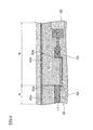
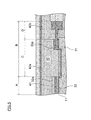
- FIGS. 4 and 5 are cross-sectional views illustrating the modification examples of the connector assembly in the present embodiment.
- the connector assembly 1 of the present embodiment has a configuration in which a transmission cable compliant with the High-Definition Multimedia Interface (HDMI: registered trademark) standards, for example, is connected to a connector.
- HDMI High-Definition Multimedia Interface
- the connector assembly 1 is used when electrically connecting electronic apparatuses such as a television and a PC.
- the connector assembly 1 may be applied to Universal Serial Bus (USB) 3.0 connectors and Display Port connectors.
- USB Universal Serial Bus
- the connector assembly 1 of the present embodiment comprises a connector 10, a cable 20, a wiring board 30, an insulating material 40, a connector shielding layer 50, and an insulating cover layer 60, as illustrated in FIGS. 1 and 2 .
- the connector 10 is fitted to another connector (for example, a HDMI terminal) corresponding to the connector assembly 1 to thereby electrically connect the other connector and the cable 20.
- the connector 10 is provided with a plurality of contact terminals 11 (see FIGS. 2 and 3 ) which serves as electrical contact points with the other connector.
- nineteen contact terminals 11 are provided in the connector 10 of the present embodiment, the number of contact terminals 11 is not particularly limited. The number of contact terminals 11 can be appropriately set in accordance with the number of terminals of the other connector. In FIG. 3 , only five contact terminals 11 of the nineteen contact terminals are illustrated, and the remaining fourteen contact terminals 11 are not illustrated.
- the cable 20 includes a cable unit 21 in which two insulating wires 22 are covered together by a cable shielding layer 23 as illustrated in FIG. 2 .
- the insulating wires 22 are electromagnetically shielded from the outside by the cable shielding layer 23.
- one insulating wire 22 of the two insulating wires 22 is not illustrated.
- the insulating wire 22 has a configuration in which a conductor 221 transmitting electrical signals is covered by a cable insulating layer 222 as illustrated in the drawing.
- a drain line for electrically connecting the cable shielding layer 23 and the ground (GND) is provided in the cable unit 21.
- the cable 20 of the present embodiment includes four such cable units 21 in total. Moreover, the cable 20 includes seven insulating wires in addition to the four cable units 21. Thus, nineteen insulating wires 22 and drain lines in total are provided in the cable 20, and these nineteen insulating wires 22 and drain lines are electrically connected to nineteen contact terminals 11 of the connector 10 via the wiring board 30.
- the insulating wire 22 is covered by the cable shielding layer 23 in a cable body portion 20a of the cable 20.
- the insulating wire 22 is exposed from the cable shielding layer 23, and the conductor 221 is exposed from the insulating wire 22.
- the conductor 221 is connected by soldering to a second connecting portion 33 described later, of the wiring board 30.
- the impedance of the cable exposed portion 20b exposed from the cable shielding layer 23 is likely to be affected by the external environment.
- the wiring board 30 includes an insulating substrate 31, first connecting portions 32, second connecting portions 33, and wiring lines 34.
- the insulating substrate 31 is a substrate composed of a glass epoxy-based resin, for example, and is disposed between the connector 10 and the cable 20.
- the first connecting portions 32 are configured to electrically connect the contact terminals 11 of the connector 10 and the wiring lines 34. As illustrated in FIG. 2 , the first connecting portions 32 are connected by soldering to the contact terminals 11 by solders 32a in a state where the first connecting portions 32 are exposed from the insulating substrate 31. In the present embodiment, since the first connecting portions 32 are exposed from the insulating substrate 31, the impedance of the first connecting portions 32 is likely to be affected by the external environment.
- nineteen first connecting portions 32 are provided on the wiring board 30 so as to correspond to the nineteen contact terminals 11 of the connector 10.
- nine first connecting portions 32 are disposed on one main surface 31 a of the insulating substrate 31 (five of the nine first connecting portions 32 are not illustrated).
- Ten first connecting portions are disposed on the another main surface of the insulating substrate 31.
- the number of first connecting portions 32 is not limited to 19, and the number can be appropriately set in accordance with the number of contact terminals 11.
- first connecting portions 32 are arranged at a relatively small first pitch P 1 in the plan view illustrated in FIG. 3 .
- the second connecting portions 33 are configured to electrically connect the conductors 221 of the cable 20 and the wiring lines 34. As illustrated in FIG. 2 , the second connecting portions 33 are connected by soldering to the conductors 221 by solders 33a in a state where the second connecting portions 33 are exposed from the insulating substrate 31. Since the second connecting portions 33 are exposed from the insulating substrate 31, the impedance of the second connecting portions 33 is likely to be affected by the external environment.
- nineteen second connecting portions 33 are provided on the wiring board 30 so as to correspond to the nineteen insulating wires 22 and drain lines of the cable 20.
- nine second connecting portions 33 are disposed on one main surface 31a of the insulating substrate 31 (five of the nine second connecting portions 33 are not illustrated).
- Ten second connecting portions (not illustrated) are disposed on the another main surface of the insulating substrate 31.
- the number of second connecting portions 33 is not limited to 19, and the number can be appropriately set in accordance with the number of insulating wires 22 or drain lines of the cable 20.
- these second connecting portions 33 are arranged at a second pitch P 2 in the plan view illustrated in FIG. 3 .
- the second pitch P 2 of the second connecting portions 33 is relatively larger than the first pitch P 1 of the first connecting portions 32 (P 1 ⁇ P 2 ).
- P 1 ⁇ P 2 the first pitch P 1 of the first connecting portions 32
- the wiring lines 34 are configured to electrically connect the first connecting portions 32 and the second connecting portions 33.
- nineteen wiring lines 34 are provided so as to correspond to the nineteen first connecting portions 32 and the nineteen second connecting portions 33.
- the number of wiring lines 34 is not limited to 19, and the number can be appropriately set in accordance with the number of first connecting portions 32 and second connecting portions 33.
- the wiring lines 34 are embedded in the insulating substrate 31.
- One end of the wiring line 34 is exposed from the insulating substrate 31 and connected to the lower portion of the first connecting portion 32, and the another end thereof is exposed from the insulating substrate 31 and connected to the lower portion of the second connecting portion 33.
- the impedance of the wiring lines 34 is unlikely to be affected by the external environment.
- the pitch of the wiring lines 34 changes continuously between the first pitch P 1 of the first connecting portions 32 and the second pitch P 2 of the second connecting portions 33 as in the plan view illustrated in FIG. 3 . That is, these wiring lines 34 electrically connect the first connecting portions 32 and the second connecting portions 33 while switching the pitch thereof between the first pitch P 1 of the first connecting portions 32 and the second pitch P 2 of the second connecting portions 33.
- the insulating material 40 surrounds the end portion of the cable 20 and the wiring board 30 to protect the end portion of the cable 20 and the wiring board 30.
- the insulating material 40 includes a first portion A configured to surround the first connecting portions 32 of the wiring board 30 and a second portion B configured to surround the wiring lines 34 and the cable exposed portion 20b.
- the second portion B of the insulating material 40 may be configured to surround at least the second connecting portions 33 of the wiring board 30 and the cable exposed portion 20b.
- the first portion A of the insulating material 40 comprises a foam 41 and a hot melt 42.
- the second portion B of the insulating material 40 comprises only the hot melt 42.
- the foam 41 is stacked on the first connecting portions 32.
- An expanded polypropylene (PP) tape may be used as the foam 41.
- the foam 41 may be one obtained by expanding polyethylene (PE), polytetrafluorotthylene (PTFE), polyethylene terephthalate (PET), acrylic resin, polyvinyl chloride (PVC), or the like.
- the foam 41 contains air therein, the foam has a smaller dielectric constant (a dielectric constant close to that of air) than a hot melt 42 (described later).
- the dielectric constant ( ⁇ eff ) of the foam 41 is preferably smaller than 3 ( ⁇ eff ⁇ 3), or the dielectric tangent tan ⁇ of the foam 41 is preferably smaller than 0.01 (tan ⁇ ⁇ 0.01).
- the foam 41 is stacked on the solders 32a that connect the first connecting portions 32 and the contact terminals 11, the present invention is not particularly limited to this.
- the foam 41 may be stacked on portion of the connector shielding layer 50 facing the first connecting portions 32, and the hot melt 42 may be interposed between the foam 41 and the first connecting portions 32.
- the hot melt 42 is configured to surround the wiring board 30 and the cable exposed portion 20b so as to fix the wiring board 30 and the cable 20. As described above, since the foam 41 is stacked on the first connecting portions 32, the hot melt 42 in the first portion A surrounds the wiring board 30 (the first connecting portions 32) via the foam 41. On the other hand, the hot melt 42 in the second portion B directly surrounds the wiring board 30 and the cable exposed portion 20b.
- the hot melt 42 may be one which has excellent heat resistance and mechanical strength, and the hot melt 42 may be composed of polyamide, polyethylene, polypropylene, or the like, for example. Instead of the hot melt 42, another insulating material may be used so as to surround the wiring board 30 and the cable exposed portion 20b.
- a first dielectric constant E 1 of the first portion A of the insulating material 40 is relatively smaller than a second dielectric constant E 2 of the second portion B of the insulating material 40 (the first dielectric constant is close to the dielectric constant of the air).
- the wiring board 30 and the cable exposed portion 20b are surrounded (disposed) by the following method.
- the tape-shaped foam 41 is disposed in the first connecting portions 32.
- the wiring board 30 and the cable exposed portion 20b are set on a die (not illustrated in particular), and the molten hot melt 42 is flowed therein.
- the hot melt 42 is cooled and solidified, whereby the insulating material 40 is disposed.
- the foam 41 air is contained in the first portion A of the insulating material 40 so that the first dielectric constant E 1 of the first portion A is smaller than the second dielectric constant E 2 of the second portion B
- the present invention is not particularly limited to this.
- the first portion A of the insulating material 40 may comprise a first hot melt 42a
- the second portion B of the insulating material 40 may comprise a second hot melt 42b.
- the dielectric constant of the first hot melt 42a is different from the dielectric constant of the second hot melt 42b.
- the dielectric constant of the first hot melt 42a is made relatively smaller than the dielectric constant of the second hot melt 42b so that the first dielectric constant E 1 of the first portion A is smaller than the second dielectric constant E 2 of the second portion B.
- the connector shielding layer 50 surrounds the insulating material 40, and the wiring board 30 and the cable exposed portion 20b are electromagnetically shielded from the outside via the insulating material 40.
- one end of the connector shielding layer 50 is soldered to the metal shell of the connector 10 and is electrically connected to the ground (GND) via the metal shell.
- Such a connector shielding layer 50 is formed of tape-shaped copper (Cu), for example.
- the material of the connector shielding layer 50 is not particularly limited as long as it has conductive properties.
- the insulating cover layer 60 is configured to surround the connector shielding layer 50 and protect the connector shielding layer 50, the wiring board 30, and the cable exposed portion 20b.
- the insulating cover layer 60 is composed of a polypropylene-based resin or an olefin-based resin, for example.
- the contact terminals 11 and the conductors 221 are connected via the wiring board 30 so that the pitch (first pitch P 1 ) of the contact terminals 11 is made relatively smaller than the pitch (second pitch P 2 ) of the conductors 221.
- the pitch (first pitch P 1 ) of the contact terminals 11 is made relatively smaller than the pitch (second pitch P 2 ) of the conductors 221.
- matching between the impedance of the first connecting portions 32, the impedance of the second connecting portions 33, and the impedance of the cable exposed portion 20b is promoted so that the transmission characteristics of the connector assembly 1 are improved.
- the first portion A of the insulating material 40 comprises the foam 41 and the hot melt 42
- the second portion B of the insulating material 40 comprises the hot melt 42 so that the first dielectric constant E 1 is made relatively smaller than the second dielectric constant E 2 (E 1 ⁇ E 2 ).
- E 1 ⁇ E 2 the second dielectric constant
- the second portion B may be configured to include: a third portion C that surrounds the wiring lines 34 and the second connecting portions 33; and a fourth portion D that is adjacent to the third portion C so as to surround a portion of the cable exposed portion 20b.
- the third portion C of the insulating material 40 and the fourth portion D of the insulating material 40 may be composed of materials having different dielectric constants.
- the third portion C of the insulating material 40 may be a portion which is configured to surround at least the second connecting portions 33 of the wiring board 30.
- "a portion of the cable exposed portion 20b" as mentioned herein is a portion of the cable exposed portion 20b which is not in contact with the second connecting portions 33.
- the first portion A of the insulating material 40 may comprise the foam 41 and the first hot melt 42a.
- the third portion C of the insulating material 40 may comprise only the first hot melt 42a.
- the fourth portion D of the insulating material 40 may comprise the second hot melt 42b having a dielectric constant different from that of the first hot melt 42a.
- the insulating material 40 is configured so that the first dielectric constant E 1 is relatively smaller than the second dielectric constant E 2 , the present invention is not particularly limited to this.
- the insulating material may be configured so that the first dielectric constant E 1 is relatively larger than the second dielectric constant E 2 depending on the structure of the first connecting portions 32, the second connecting portions 33 and the cable exposed portion 20b etc. and the impedance matching in the connector assembly is promoted.
- FIG. 6 is a cross-sectional view of a connector assembly in the present embodiment
- FIG. 7 is a perspective view illustrating a connector shielding layer of the connector assembly in the present embodiment
- FIG. 8 is a cross-sectional view along the line VIII-VIII line of FIG. 6
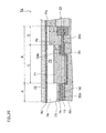
- FIG. 9 and FIG. 10 are cross-sectional views illustrating modification examples of the connector assembly in the present embodiment.
- a connector assembly 1a of the present embodiment is different from that of the first embodiment in terms of the configuration of an insulating material 70 and the configuration of a connector shielding layer 80, and the other configurations are the same as those of the first embodiment.
- the same configurations as those of the first embodiment will be denoted by the same reference numerals, and description thereof will not be provided.
- the connector shielding layer 80 of the present embodiment comprises a metal shell 81.
- the metal shell 81 includes: shell body portions 81a and 81b in which the wiring board 30 and the cable exposed portion 20b are accommodated; a shell fixing portion 81c that is bent inward so as to fix the cable 20; and a shell connecting portion 81 d that connects the shell body portion 81a and the shell fixing portion 81 c.
- the metal shell 81 is formed by bending a plate composed of stainless, for example.
- the connector shielding layer 80 comprises the metal shell 81, it is possible to fix the cable 20 without via the insulating material 70 as described above. Moreover, it is possible to fix the connector 10 and the wiring board 30 by connecting the shell body portions 81a and 81b to the connector 10. In this way, even when a gaseous insulating material 72 described later is contained in the insulating material 70, the wiring board 30 and the cable 20 are fixed inside the connector assembly 1a.
- the insulating material 70 of the present embodiment includes a solid insulating material 71 and a gaseous insulating material 72.
- the solid insulating material 71 is formed of a hot melt made from polyamide, polyethylene, polypropylene, or the like, for example, and forms a solid insulating layer 73.
- the solid insulating layer 73 directly surrounds the wiring board 30 and the cable exposed portion 20b.
- a first thickness H 1 of the solid insulating layer 73 in the first portion A is relatively smaller than a second thickness H 2 of the solid insulating layer 73 in the second portion B (H 1 ⁇ H 2 ).
- the gaseous insulating material 72 is formed of air, for example, and is interposed between the solid insulating material 71 and the connector shielding layer 80 to form a gaseous insulating layer 74. Moreover, the gaseous insulating material 72 is not particularly limited to air as long as it is formed of gas.
- the thickness relation of the gaseous insulating layer 74 is reverse to that of the solid insulating layer 73, and a third thickness H 3 of the first portion A is relatively larger than a fourth thickness H 4 of the second portion B.
- the first portion A of the insulating material 70 contains a larger amount of air (gas) than the second portion B of the insulating material 70, and the first dielectric constant E 1 of the first portion A is relatively smaller than the second dielectric constant E 2 of the second portion B (E 1 ⁇ E 2 ).
- the decrease of the impedance of the first connecting portions 32 is suppressed, and the matching between the impedance of the first connecting portions 32, the impedance of the second connecting portions 33, and the impedance of the cable exposed portion 20b is promoted. In this way, it is possible to improve the transmission characteristics of the connector assembly 1a.
- the gaseous insulating material 72 may be interposed between the solid insulating material 71 and the connector shielding layer 80, the gaseous insulating material 72 may be interposed between the wiring board 30 and the solid insulating material 71 and may be interposed between the cable exposed portion 20b and the solid insulating material 71, as illustrated in FIG. 9 .
- the present invention is not particularly limited to this, and the solid insulating layer 73 may be formed so that the first thickness H 1 is larger than the second thickness H 2 .
- the second portion B of the insulating material 70 may be configured to include: a third portion C that surrounds the wiring lines 34 and the second connecting portions 33; and a fourth portion D that is adjacent to the third portion C so as to surround the cable exposed portion 20b.
- a fifth thickness H 5 of the third portion C of the solid insulating layer 73 may be different from a sixth thickness H 6 of the fourth portion D of the solid insulating layer 73.
- the solid insulating layer 73 may be formed so that the fifth thickness H 5 is smaller than the sixth thickness H 6 (H 5 ⁇ H 6 ).
- the third portion C may be a portion which is configured to surround at least the second connecting portions 33 of the wiring board 30.
- "a portion of the cable exposed portion 20b" as mentioned herein is a portion of the cable exposed portion 20b which is not in contact with the second connecting portions 33.
- the first thickness H 1 of the first portion A, the fifth thickness H 5 of the third portion C, and the sixth thickness H 6 of the fourth portion D may be made different from each other so that the matching between the impedance of three portions of the first connecting portions 32, the second connecting portions 33, and the cable exposed portion 20b is promoted. In this way, it is possible to further improve the transmission characteristics of the connector assembly 1a.
- FIG. 11 is a cross-sectional view of a connector assembly in the present embodiment
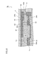
- FIG. 12 is a cross-sectional view illustrating a modification example of the connector assembly in the present embodiment.
- a connector assembly 1b of the present embodiment is different from that of the first embodiment in terms of the configuration of an insulating material 90 and the configuration of a connector shielding layer 80, and the other configurations are the same as those of the first embodiment.
- the same configurations as those of the first embodiment will be denoted by the same reference numerals, and description thereof will not be provided.
- the insulating material 90 of the present embodiment comprises only one kind of hot melt 91.
- the connector shielding layer 80 comprises the metal shell 81 similarly to the second embodiment.
- a shield plate 82 is stacked in a portion (inner surface) corresponding to the second connecting portions 33 of the wiring board 30 and the cable exposed portion 20b.
- the shield plate 82 is formed of tape-shaped copper, for example.
- an eighth thickness H 8 of a portion of the connector shielding layer 80 corresponding to the second connecting portions 33 and the cable exposed portion 20b is relatively larger than a seventh thickness H 7 of a portion of the connector shielding layer 80 corresponding to the first connecting portions 32 (H 7 ⁇ H 8 ).
- the distance L 1 from the connector shielding layer 80 to the first connecting portions 32 is relatively smaller than the distance L 2 from the connector shielding layer 80 to the second connecting portions 33 and the cable exposed portion 20b (L 1 > L 2 ).
- the impedance of the second connecting portions 33 and the impedance of the cable exposed portion 20b are decreased. In this way, it is possible to promote the matching between the impedance of the first connecting portions 32, the impedance of the second connecting portions 33, and the impedance of the cable exposed portion 20b and to improve the transmission characteristics of the connector assembly 1b.
- the shield plate 82 is stacked on the metal shell 81, the present invention is not particularly limited to this.
- the metal shell 81 may be formed integrally so that the eighth thickness H 8 of the portion of the connector shielding layer 80 corresponding to the second connecting portions 33 and the cable exposed portion 20b is relatively larger than the seventh thickness H 7 of the portion of the connector shielding layer 80 corresponding to the first connecting portions 32.
- the metal shell 81 may be formed so that the portion of the connector shielding layer 80 corresponding to the second connecting portions 33 and the cable exposed portion 20b protrude inward in a convex shape more than the portion of the connector shielding layer 80 corresponding to the first connecting portions 32.
- the eighth thickness H 8 is relatively larger than the seventh thickness H 7
- the present invention is not particularly limited to this.
- the eighth thickness H 8 may be made relatively smaller than the seventh thickness H 7
- the distance L 2 from the connector shielding layer 80 to the second connecting portions 33 and the cable exposed portion 20b may be made relatively larger than the distance L 1 from the connector shielding layer 80 to the first connecting portions 32.
- the connector shielding layer 80 may be configured so that a distance L 3 from the connector shielding layer 80 to the second connecting portions 33 is different from a distance L 4 from the connector shielding layer 80 to the cable exposed portion 20b.
- a shield plate 82a may be further stacked on a portion (inner surface) of the shell body portion 81b corresponding to the cable exposed portion 20b, and the distance L 4 from the connector shielding layer 80 to the cable exposed portion 20b may be made relatively smaller than the distance L 3 from the connector shielding layer 80 to the second connecting portions 33 (L 3 > L 4 ).
- the distance L 1 from the connector shielding layer 80 to the first connecting portions 32, the distance L 3 from the connector shielding layer 80 to the second connecting portions 32, and the distance L 4 from the connector shielding layer 80 to the cable exposed portion 20b may be made different from each other so that the matching between the impedance of three portions of the first connecting portions 32, the second connecting portions 33, and the cable exposed portion 20b can be promoted. In this way, it is possible to further improve the transmission characteristics of the connector assembly 1b.
- foam may be stacked on the first connecting portions 32 similarly to the first embodiment. In this way, the impedance matching of the connector assembly 1b can be further improved.
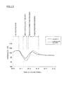
- FIG. 13 is a graph illustrating the impedance of Example and Comparative Example for comparison.
- Example 1 a sample having the same structure as the first embodiment described above was prepared.
- a polypropylene tape expanded to have a dielectric constant of about 2.0 was used as foam
- polyamide having a dielectric constant of 3.3 to 3.6 was used as a hot melt
- a copper tape was used as a connector shielding layer.
- the impedance from the connector to the cable was measured for the sample of Example.
- a sampling oscilloscope TDS8000, product of Japan Tektronix INC.
- the measurement results of Example are illustrated in FIG. 13 .
- the vertical axis of FIG. 13 represents impedance ( ⁇ ).
- the horizontal axis of FIG. 13 represents signal transmission time (nano seconds) which signifies a portion of the connector assembly. 41.0 nano seconds siginifies the connector, about 41.2 nano seconds signifies the first connecting portion, and 41.4 to 41.5 nano seconds signifies a portion between the second connecting portion and the cable exposed portion.
- Comparative Example 1 a sample having the same structure as Example 1 was prepared except that the insulating material comprises only a hot melt. The impedance was measured for the sample of Comparative Example by the same method as Example 1. The measurement results of Comparative Example are illustrated in FIG. 13 .
- Comparative Example 1 As illustrated in FIG. 13 , the impedance is extremely low in the first connecting portion. This is considered to be attributable to the fact that only the hot melt having a larger dielectric constant than air is stacked on the first connecting portion.
- Example 1 As illustrated in FIG. 13 , the decrease of the impedance in the first connecting portion is suppressed as compared to Comparative Example 1. This is considered to be attributable to the fact that since the foam and the hot melt surrounded the first connecting portion in Example 1, the first dielectric constant E 1 in the first portion of the insulating material decreases, and the decrease of the impedance in the first connecting portion is suppressed.
- the first portion of the insulating material comprises the foam and the hot melt
- the second portion of the insulating material comprises the hot melt so that the first dielectric constant E 1 is made relatively smaller than the second dielectric constant E 2 , the matching between the impedance of the first connecting portion, and the second connecting portion and the cable exposed portion is promoted.
Landscapes
- Details Of Connecting Devices For Male And Female Coupling (AREA)
- Coupling Device And Connection With Printed Circuit (AREA)
- Multi-Conductor Connections (AREA)
Abstract
Description
- The present invention relates to a connector assembly in which a cable and a connector are electrically connected via a wiring board.
- It is to be noted that, for those designated countries which permit the incorporation by reference, the contents described and/or illustrated in the documents relevant to Japanese Patent Application No.
2010-043835, filed on March 1, 2010 - An electrical connector in which connection terminals disposed in a connector housing and conductors of a cable are directly connected is known (for example, refer to Patent Literature 1).
- Patent Literature 1: International Patent Laid-Open No. 2004-015822
- In the electrical connector described above, since the connection between the connection terminals and the conductors is realized by soldering or spot welding, it is necessary to secure a sufficient pitch between connection terminals in order to suppress short-circuiting between adjacent connection terminals. As a result, the electrical connector has a large size.
- An object of the present invention is to provide a connector assembly capable of decreasing the size of a connector.
- A connector assembly according to the present invention is a connector assembly comprising: a connector including contact terminals; a cable including conductors; and a wiring board which electrically connects the connector and the cable, the connector assembly characterized in that the wiring board includes: first connecting portions which are arranged at a first pitch and to which the contact terminals are electrically connected; second connecting portions which are arranged at a second pitch and to which the conductors of the cable are electrically connected; and wiring lines which electrically connect the first connecting portions and the second connecting portions, and the first pitch is smaller than the second pitch.
- In the above-mentioned invention, the cable may include a cable exposed portion in which insulating wires including the conductors are exposed from a cable shielding layer and the conductors are exposed from the insulating wires, the connector assembly may further comprise: a connector shielding layer which is provided around the wiring board and the cable exposed portion; and an insulating material which is interposed between the connector shielding layer and the wiring board and which is interposed between the connector shielding layer and the cable exposed portion, a dielectric constant of a first portion of the insulating material may be different from a dielectric constant of a second portion of the insulation material, the first portion may surround the first connecting portions in the insulating material, and the second portion may surrounds the second connecting portions in the insulating material.
- In the above-mentioned invention, the first portion of the insulating material may comprise a hot melt and a foam, and the second portion of the insulating material may comprise the hot melt.
- In the above-mentioned invention, the first portion of the insulating material may comprise a first hot melt, and the second portion of the insulating material may comprise a second hot melt which has a dielectric constant different from that of the first hot melt.
- In the above-mentioned invention, the second portion may include: a third portion which surrounds the second connecting portions; and a fourth portion which is adjacent to the third portion and which surrounds the cable exposed portion, and a dielectric constant of the third portion of the insulating material may be different from a dielectric constant of the fourth portion of the insulating material.
- In the above-mentioned invention, the insulating material may include a solid insulating material and a gaseous insulating material, the gaseous insulating material may be interposed between the solid insulating material and the connector shielding layer, or the gaseous insulating material may be interposed between the solid insulating material and the wiring board and is interposed between the solid insulating material and the cable exposed portion, and a thickness of the first portion of the solid insulating material may be different from a thickness of the second portion of the solid insulating material.
- In the above-mentioned invention, the second portion may include: a third portion which surrounds the second connecting portions; and a fourth portion which is adjacent to the third portion and which surrounds the cable exposed portion, and a thickness of the third portion of the solid insulating material may be different from a thickness of the fourth portion of the solid insulating material.
- A connector assembly according to the present invention is a connector assembly comprising: a connector; a cable including a cable exposed portion in which insulating wires including conductors is exposed from a cable shielding layer and the conductors are exposed from the insulating wires; a wiring board which electrically connects the connector and the cable; a connector shielding layer which is provided around the wiring board and the cable exposed portion; and an insulating material which is interposed between the connector shielding layer and the wiring board and which is interposed between the connector shielding layer and the cable exposed portion, characterized in that the wiring board includes: first connecting portions to which the connector is electrically connected; second connecting portions to which the conductors of the cable are electrically connected, and wiring lines which electrically connect the first connecting portions and the second connecting portions, and a distance from the connector shielding layer to the first connecting portions is different from a distance from the connector shielding layer to the second connecting portions and the cable exposed portion.
- In the above-mentioned invention, a distance from the connector shielding layer to the second connecting portions may be different from a distance from the connector shielding layer to the cable exposed portion.
- According to the present invention, since the first pitch of the first connecting portions of the wiring board, to which the contact terminals are electrically connected, is smaller than the second pitch of the second connecting portions to which the conductors are electrically connected, it is possible to decrease the size of the connector.
-
-
FIG. 1 is a perspective view of a connector assembly in a first embodiment of the present invention. -
FIG. 2 is a cross-sectional view along the line II-II ofFIG. 1 . -
FIG. 3 is a cross-sectional view along the line III-III ofFIG. 2 . -
FIG. 4 is a cross-sectional view illustrating a first modification example of the connector assembly in the first embodiment of the present invention. -
FIG. 5 is a cross-sectional view illustrating a second modification example of the connector assembly in the first embodiment of the present invention. -
FIG. 6 is a cross-sectional view of a connector assembly in a second embodiment of the present invention. -
FIG. 7 is a perspective view illustrating a connector shielding layer of the connector assembly in the second embodiment of the present invention. -
FIG. 8 is a cross-sectional view along the line VIII-VIII ofFIG. 6 . -
FIG. 9 is a cross-sectional view illustrating a first modification example of the connector assembly in the second embodiment of the present invention. -
FIG. 10 is a cross-sectional view illustrating a second modification example of the connector assembly in the second embodiment of the present invention. -
FIG. 11 is a cross-sectional view of a connector assembly in a third embodiment of the present invention. -
FIG. 12 is a cross-sectional view illustrating a modification example of the connector assembly in the third embodiment of the present invention. -
FIG. 13 is a graph illustrating the impedance of Example and Comparative Example for comparison. - Hereinafter, embodiments of the present invention will be described based on the drawings.
-
FIG. 1 is a perspective view of a connector assembly in the present embodiment,FIG. 2 is a cross-sectional view along the line II-II ofFIG. 1 ,FIG. 3 is a cross-sectional view along the line III-III ofFIG. 2 , andFIGS. 4 and 5 are cross-sectional views illustrating the modification examples of the connector assembly in the present embodiment. - The
connector assembly 1 of the present embodiment has a configuration in which a transmission cable compliant with the High-Definition Multimedia Interface (HDMI: registered trademark) standards, for example, is connected to a connector. Theconnector assembly 1 is used when electrically connecting electronic apparatuses such as a television and a PC. Theconnector assembly 1 may be applied to Universal Serial Bus (USB) 3.0 connectors and Display Port connectors. - The
connector assembly 1 of the present embodiment comprises aconnector 10, acable 20, awiring board 30, aninsulating material 40, aconnector shielding layer 50, and aninsulating cover layer 60, as illustrated inFIGS. 1 and2 . - The
connector 10 is fitted to another connector (for example, a HDMI terminal) corresponding to theconnector assembly 1 to thereby electrically connect the other connector and thecable 20. Theconnector 10 is provided with a plurality of contact terminals 11 (seeFIGS. 2 and3 ) which serves as electrical contact points with the other connector. Although nineteencontact terminals 11 are provided in theconnector 10 of the present embodiment, the number ofcontact terminals 11 is not particularly limited. The number ofcontact terminals 11 can be appropriately set in accordance with the number of terminals of the other connector. InFIG. 3 , only fivecontact terminals 11 of the nineteen contact terminals are illustrated, and the remaining fourteencontact terminals 11 are not illustrated. - The
cable 20 includes acable unit 21 in which twoinsulating wires 22 are covered together by acable shielding layer 23 as illustrated inFIG. 2 . Within thecable unit 21, theinsulating wires 22 are electromagnetically shielded from the outside by thecable shielding layer 23. In the drawing, oneinsulating wire 22 of the twoinsulating wires 22 is not illustrated. The insulatingwire 22 has a configuration in which aconductor 221 transmitting electrical signals is covered by acable insulating layer 222 as illustrated in the drawing. - Although not particularly illustrated, a drain line for electrically connecting the
cable shielding layer 23 and the ground (GND) is provided in thecable unit 21. - The
cable 20 of the present embodiment includes foursuch cable units 21 in total. Moreover, thecable 20 includes seven insulating wires in addition to the fourcable units 21. Thus, nineteeninsulating wires 22 and drain lines in total are provided in thecable 20, and these nineteeninsulating wires 22 and drain lines are electrically connected to nineteencontact terminals 11 of theconnector 10 via thewiring board 30. - Here, as illustrated in
FIG. 2 , theinsulating wire 22 is covered by thecable shielding layer 23 in acable body portion 20a of thecable 20. In a cable exposedportion 20b positioned at the end portion of thecable body portion 20a, theinsulating wire 22 is exposed from thecable shielding layer 23, and theconductor 221 is exposed from theinsulating wire 22. Moreover, in the cable exposedportion 20b, theconductor 221 is connected by soldering to a second connectingportion 33 described later, of thewiring board 30. As above, the impedance of the cable exposedportion 20b exposed from thecable shielding layer 23 is likely to be affected by the external environment. - As illustrated in
FIGS. 2 and3 , thewiring board 30 includes aninsulating substrate 31, first connectingportions 32, second connectingportions 33, andwiring lines 34. - As illustrated in
FIGS. 2 and3 , theinsulating substrate 31 is a substrate composed of a glass epoxy-based resin, for example, and is disposed between theconnector 10 and thecable 20. - The first connecting
portions 32 are configured to electrically connect thecontact terminals 11 of theconnector 10 and thewiring lines 34. As illustrated inFIG. 2 , the first connectingportions 32 are connected by soldering to thecontact terminals 11 bysolders 32a in a state where the first connectingportions 32 are exposed from the insulatingsubstrate 31. In the present embodiment, since the first connectingportions 32 are exposed from the insulatingsubstrate 31, the impedance of the first connectingportions 32 is likely to be affected by the external environment. - Here, nineteen first connecting
portions 32 are provided on thewiring board 30 so as to correspond to the nineteencontact terminals 11 of theconnector 10. In the present embodiment, as illustrated inFIG. 3 , nine first connectingportions 32 are disposed on onemain surface 31 a of the insulating substrate 31 (five of the nine first connectingportions 32 are not illustrated). Ten first connecting portions (not illustrated) are disposed on the another main surface of the insulatingsubstrate 31. The number of first connectingportions 32 is not limited to 19, and the number can be appropriately set in accordance with the number ofcontact terminals 11. - Moreover, these first connecting
portions 32 are arranged at a relatively small first pitch P1 in the plan view illustrated inFIG. 3 . - The second connecting
portions 33 are configured to electrically connect theconductors 221 of thecable 20 and the wiring lines 34. As illustrated inFIG. 2 , the second connectingportions 33 are connected by soldering to theconductors 221 bysolders 33a in a state where the second connectingportions 33 are exposed from the insulatingsubstrate 31. Since the second connectingportions 33 are exposed from the insulatingsubstrate 31, the impedance of the second connectingportions 33 is likely to be affected by the external environment. - Here, nineteen second connecting
portions 33 are provided on thewiring board 30 so as to correspond to the nineteen insulatingwires 22 and drain lines of thecable 20. In the present embodiment, as illustrated inFIG. 3 , nine second connectingportions 33 are disposed on onemain surface 31a of the insulating substrate 31 (five of the nine second connectingportions 33 are not illustrated). Ten second connecting portions (not illustrated) are disposed on the another main surface of the insulatingsubstrate 31. The number of second connectingportions 33 is not limited to 19, and the number can be appropriately set in accordance with the number of insulatingwires 22 or drain lines of thecable 20. - Moreover, these second connecting
portions 33 are arranged at a second pitch P2 in the plan view illustrated inFIG. 3 . As illustrated in the drawing, the second pitch P2 of the second connectingportions 33 is relatively larger than the first pitch P1 of the first connecting portions 32 (P1 < P2). As above, by arranging the second connectingportions 33 at the relatively large second pitch P2, it is possible to suppress the short-circuiting of theconductors 221 when connecting theconductors 221 and the second connectingportions 33. - As illustrated in
FIGS. 2 and3 , thewiring lines 34 are configured to electrically connect the first connectingportions 32 and the second connectingportions 33. In thewiring board 30 of the present embodiment, nineteenwiring lines 34 are provided so as to correspond to the nineteen first connectingportions 32 and the nineteen second connectingportions 33. The number ofwiring lines 34 is not limited to 19, and the number can be appropriately set in accordance with the number of first connectingportions 32 and second connectingportions 33. - As illustrated in
FIG. 2 , thewiring lines 34 are embedded in the insulatingsubstrate 31. One end of thewiring line 34 is exposed from the insulatingsubstrate 31 and connected to the lower portion of the first connectingportion 32, and the another end thereof is exposed from the insulatingsubstrate 31 and connected to the lower portion of the second connectingportion 33. - As above, in the present embodiment, since the
wiring lines 34 are embedded in the insulatingsubstrate 31, the impedance of the wiring lines 34 is unlikely to be affected by the external environment. - Moreover, in the present embodiment, the pitch of the
wiring lines 34 changes continuously between the first pitch P1 of the first connectingportions 32 and the second pitch P2 of the second connectingportions 33 as in the plan view illustrated inFIG. 3 . That is, thesewiring lines 34 electrically connect the first connectingportions 32 and the second connectingportions 33 while switching the pitch thereof between the first pitch P1 of the first connectingportions 32 and the second pitch P2 of the second connectingportions 33. - As illustrated in
FIG. 2 , the insulatingmaterial 40 surrounds the end portion of thecable 20 and thewiring board 30 to protect the end portion of thecable 20 and thewiring board 30. - The insulating
material 40 includes a first portion A configured to surround the first connectingportions 32 of thewiring board 30 and a second portion B configured to surround thewiring lines 34 and the cable exposedportion 20b. The second portion B of the insulatingmaterial 40 may be configured to surround at least the second connectingportions 33 of thewiring board 30 and the cable exposedportion 20b. - As illustrated in
FIG. 2 , the first portion A of the insulatingmaterial 40 comprises afoam 41 and ahot melt 42. On the other hand, as illustrated in the drawing, the second portion B of the insulatingmaterial 40 comprises only thehot melt 42. - As illustrated in the drawing, the
foam 41 is stacked on the first connectingportions 32. An expanded polypropylene (PP) tape may be used as thefoam 41. Thefoam 41 may be one obtained by expanding polyethylene (PE), polytetrafluorotthylene (PTFE), polyethylene terephthalate (PET), acrylic resin, polyvinyl chloride (PVC), or the like. - Since the
foam 41 contains air therein, the foam has a smaller dielectric constant (a dielectric constant close to that of air) than a hot melt 42 (described later). Specifically, the dielectric constant (εeff) of thefoam 41 is preferably smaller than 3 (εeff < 3), or the dielectric tangent tanδ of thefoam 41 is preferably smaller than 0.01 (tanδ < 0.01). - In the present embodiment, although the
foam 41 is stacked on thesolders 32a that connect the first connectingportions 32 and thecontact terminals 11, the present invention is not particularly limited to this. For example, thefoam 41 may be stacked on portion of theconnector shielding layer 50 facing the first connectingportions 32, and thehot melt 42 may be interposed between thefoam 41 and the first connectingportions 32. - The
hot melt 42 is configured to surround thewiring board 30 and the cable exposedportion 20b so as to fix thewiring board 30 and thecable 20. As described above, since thefoam 41 is stacked on the first connectingportions 32, thehot melt 42 in the first portion A surrounds the wiring board 30 (the first connecting portions 32) via thefoam 41. On the other hand, thehot melt 42 in the second portion B directly surrounds thewiring board 30 and the cable exposedportion 20b. Thehot melt 42 may be one which has excellent heat resistance and mechanical strength, and thehot melt 42 may be composed of polyamide, polyethylene, polypropylene, or the like, for example. Instead of thehot melt 42, another insulating material may be used so as to surround thewiring board 30 and the cable exposedportion 20b. - As described above, in the present embodiment, since the foam 41 (air) is contained in only the first portion A of the insulating
material 40, a first dielectric constant E1 of the first portion A of the insulatingmaterial 40 is relatively smaller than a second dielectric constant E2 of the second portion B of the insulating material 40 (the first dielectric constant is close to the dielectric constant of the air). - In such an insulating
material 40, thewiring board 30 and the cable exposedportion 20b are surrounded (disposed) by the following method. First, the tape-shapedfoam 41 is disposed in the first connectingportions 32. Subsequently, thewiring board 30 and the cable exposedportion 20b are set on a die (not illustrated in particular), and the moltenhot melt 42 is flowed therein. Subsequently, thehot melt 42 is cooled and solidified, whereby the insulatingmaterial 40 is disposed. - In the present embodiment, although the foam 41 (air) is contained in the first portion A of the insulating
material 40 so that the first dielectric constant E1 of the first portion A is smaller than the second dielectric constant E2 of the second portion B, the present invention is not particularly limited to this. For example, as illustrated inFIG. 4 , the first portion A of the insulatingmaterial 40 may comprise a firsthot melt 42a, and the second portion B of the insulatingmaterial 40 may comprise a secondhot melt 42b. In this case, the dielectric constant of the firsthot melt 42a is different from the dielectric constant of the secondhot melt 42b. For example, the dielectric constant of the firsthot melt 42a is made relatively smaller than the dielectric constant of the secondhot melt 42b so that the first dielectric constant E1 of the first portion A is smaller than the second dielectric constant E2 of the second portion B. - Returning to
FIG. 2 , theconnector shielding layer 50 surrounds the insulatingmaterial 40, and thewiring board 30 and the cable exposedportion 20b are electromagnetically shielded from the outside via the insulatingmaterial 40. Although not illustrated in particular, one end of theconnector shielding layer 50 is soldered to the metal shell of theconnector 10 and is electrically connected to the ground (GND) via the metal shell. - Such a
connector shielding layer 50 is formed of tape-shaped copper (Cu), for example. The material of theconnector shielding layer 50 is not particularly limited as long as it has conductive properties. - As illustrated in
FIG. 2 , the insulatingcover layer 60 is configured to surround theconnector shielding layer 50 and protect theconnector shielding layer 50, thewiring board 30, and the cable exposedportion 20b. The insulatingcover layer 60 is composed of a polypropylene-based resin or an olefin-based resin, for example. - Next, the effect of the present embodiment will be described.
- In the present embodiment, the
contact terminals 11 and theconductors 221 are connected via thewiring board 30 so that the pitch (first pitch P1) of thecontact terminals 11 is made relatively smaller than the pitch (second pitch P2) of theconductors 221. Thus, it is possible to decrease the size of theconnector 10. - Moreover, in the present embodiment, matching between the impedance of the first connecting
portions 32, the impedance of the second connectingportions 33, and the impedance of the cable exposedportion 20b is promoted so that the transmission characteristics of theconnector assembly 1 are improved. - Specifically, as illustrated in
FIG. 2 , the first portion A of the insulatingmaterial 40 comprises thefoam 41 and thehot melt 42, and the second portion B of the insulatingmaterial 40 comprises thehot melt 42 so that the first dielectric constant E1 is made relatively smaller than the second dielectric constant E2 (E1 < E2). In this way, the decrease of the impedance of the first connectingportions 32 is suppressed, and the matching between the impedance of the first connectingportions 32, the impedance of the second connectingportions 33, and the impedance of the cable exposedportion 20b is promoted. - Furthermore, the second portion B may be configured to include: a third portion C that surrounds the
wiring lines 34 and the second connectingportions 33; and a fourth portion D that is adjacent to the third portion C so as to surround a portion of the cable exposedportion 20b. The third portion C of the insulatingmaterial 40 and the fourth portion D of the insulatingmaterial 40 may be composed of materials having different dielectric constants. The third portion C of the insulatingmaterial 40 may be a portion which is configured to surround at least the second connectingportions 33 of thewiring board 30. Moreover, "a portion of the cable exposedportion 20b" as mentioned herein is a portion of the cable exposedportion 20b which is not in contact with the second connectingportions 33. - For example, as illustrated in
FIG. 5 , the first portion A of the insulatingmaterial 40 may comprise thefoam 41 and the firsthot melt 42a. The third portion C of the insulatingmaterial 40 may comprise only the firsthot melt 42a. The fourth portion D of the insulatingmaterial 40 may comprise the secondhot melt 42b having a dielectric constant different from that of the firsthot melt 42a. In this way, since the matching between the impedance of three portions of the first connectingportions 32, the second connectingportions 33, and the cable exposedportion 20b can be promoted, it is possible to further improve the transmission characteristics of theconnector assembly 1. - In the present embodiment, although the insulating
material 40 is configured so that the first dielectric constant E1 is relatively smaller than the second dielectric constant E2, the present invention is not particularly limited to this. For example, if the pitch P1 of the first connectingportions 32 decreases, since the impedance relation may be reversed, the insulating material may be configured so that the first dielectric constant E1 is relatively larger than the second dielectric constant E2 depending on the structure of the first connectingportions 32, the second connectingportions 33 and the cable exposedportion 20b etc. and the impedance matching in the connector assembly is promoted. - Next, a second embodiment will be described.
-
FIG. 6 is a cross-sectional view of a connector assembly in the present embodiment,FIG. 7 is a perspective view illustrating a connector shielding layer of the connector assembly in the present embodiment,FIG. 8 is a cross-sectional view along the line VIII-VIII line ofFIG. 6 , andFIG. 9 andFIG. 10 are cross-sectional views illustrating modification examples of the connector assembly in the present embodiment. - A
connector assembly 1a of the present embodiment is different from that of the first embodiment in terms of the configuration of an insulatingmaterial 70 and the configuration of aconnector shielding layer 80, and the other configurations are the same as those of the first embodiment. In the following description, only the differences from the first embodiment will be described, and the same configurations as those of the first embodiment will be denoted by the same reference numerals, and description thereof will not be provided. - As illustrated in
FIG. 7 , theconnector shielding layer 80 of the present embodiment comprises ametal shell 81. - The
metal shell 81 includes:shell body portions wiring board 30 and the cable exposedportion 20b are accommodated; ashell fixing portion 81c that is bent inward so as to fix thecable 20; and ashell connecting portion 81 d that connects theshell body portion 81a and theshell fixing portion 81 c. Themetal shell 81 is formed by bending a plate composed of stainless, for example. - In the present embodiment, since the
connector shielding layer 80 comprises themetal shell 81, it is possible to fix thecable 20 without via the insulatingmaterial 70 as described above. Moreover, it is possible to fix theconnector 10 and thewiring board 30 by connecting theshell body portions connector 10. In this way, even when a gaseous insulatingmaterial 72 described later is contained in the insulatingmaterial 70, thewiring board 30 and thecable 20 are fixed inside theconnector assembly 1a. - As illustrated in
FIG. 8 , the insulatingmaterial 70 of the present embodiment includes a solid insulatingmaterial 71 and a gaseous insulatingmaterial 72. - The solid insulating
material 71 is formed of a hot melt made from polyamide, polyethylene, polypropylene, or the like, for example, and forms a solid insulatinglayer 73. - As illustrated in the drawing, the solid insulating
layer 73 directly surrounds thewiring board 30 and the cable exposedportion 20b. In the present embodiment, a first thickness H1 of the solid insulatinglayer 73 in the first portion A is relatively smaller than a second thickness H2 of the solid insulatinglayer 73 in the second portion B (H1 < H2). - The gaseous insulating
material 72 is formed of air, for example, and is interposed between the solid insulatingmaterial 71 and theconnector shielding layer 80 to form a gaseous insulatinglayer 74. Moreover, the gaseous insulatingmaterial 72 is not particularly limited to air as long as it is formed of gas. - The thickness relation of the gaseous insulating
layer 74 is reverse to that of the solid insulatinglayer 73, and a third thickness H3 of the first portion A is relatively larger than a fourth thickness H4 of the second portion B. - As above, in the present embodiment, the first portion A of the insulating
material 70 contains a larger amount of air (gas) than the second portion B of the insulatingmaterial 70, and the first dielectric constant E1 of the first portion A is relatively smaller than the second dielectric constant E2 of the second portion B (E1 < E2). Thus, the decrease of the impedance of the first connectingportions 32 is suppressed, and the matching between the impedance of the first connectingportions 32, the impedance of the second connectingportions 33, and the impedance of the cable exposedportion 20b is promoted. In this way, it is possible to improve the transmission characteristics of theconnector assembly 1a. - In the present embodiment, although the gaseous insulating
material 72 is interposed between the solid insulatingmaterial 71 and theconnector shielding layer 80, the gaseous insulatingmaterial 72 may be interposed between thewiring board 30 and the solid insulatingmaterial 71 and may be interposed between the cable exposedportion 20b and the solid insulatingmaterial 71, as illustrated inFIG. 9 . - Moreover, in the present embodiment, although the first thickness H1 is relatively smaller than the second thickness H2, the present invention is not particularly limited to this, and the solid insulating
layer 73 may be formed so that the first thickness H1 is larger than the second thickness H2. - Moreover, as illustrated in
FIG. 10 , the second portion B of the insulatingmaterial 70 may be configured to include: a third portion C that surrounds thewiring lines 34 and the second connectingportions 33; and a fourth portion D that is adjacent to the third portion C so as to surround the cable exposedportion 20b. A fifth thickness H5 of the third portion C of the solid insulatinglayer 73 may be different from a sixth thickness H6 of the fourth portion D of the solid insulatinglayer 73. For example, the solid insulatinglayer 73 may be formed so that the fifth thickness H5 is smaller than the sixth thickness H6 (H5<H6). The third portion C may be a portion which is configured to surround at least the second connectingportions 33 of thewiring board 30. Moreover, "a portion of the cable exposedportion 20b" as mentioned herein is a portion of the cable exposedportion 20b which is not in contact with the second connectingportions 33. - As above, in the solid insulating
layer 73, the first thickness H1 of the first portion A, the fifth thickness H5 of the third portion C, and the sixth thickness H6 of the fourth portion D may be made different from each other so that the matching between the impedance of three portions of the first connectingportions 32, the second connectingportions 33, and the cable exposedportion 20b is promoted. In this way, it is possible to further improve the transmission characteristics of theconnector assembly 1a. - Next, a third embodiment will be described.
-
FIG. 11 is a cross-sectional view of a connector assembly in the present embodiment, andFIG. 12 is a cross-sectional view illustrating a modification example of the connector assembly in the present embodiment. - A
connector assembly 1b of the present embodiment is different from that of the first embodiment in terms of the configuration of an insulatingmaterial 90 and the configuration of aconnector shielding layer 80, and the other configurations are the same as those of the first embodiment. In the following description, only the differences from the first embodiment will be described, and the same configurations as those of the first embodiment will be denoted by the same reference numerals, and description thereof will not be provided. - The insulating
material 90 of the present embodiment comprises only one kind ofhot melt 91. - The
connector shielding layer 80 comprises themetal shell 81 similarly to the second embodiment. In the present embodiment, in theshell body portion 81b in which thewiring board 30 and the cable exposedportion 20b are accommodated, ashield plate 82 is stacked in a portion (inner surface) corresponding to the second connectingportions 33 of thewiring board 30 and the cable exposedportion 20b. Theshield plate 82 is formed of tape-shaped copper, for example. - In the
connector assembly 1b of the present embodiment, an eighth thickness H8 of a portion of theconnector shielding layer 80 corresponding to the second connectingportions 33 and the cable exposedportion 20b is relatively larger than a seventh thickness H7 of a portion of theconnector shielding layer 80 corresponding to the first connecting portions 32 (H7 < H8). - That is, in the
connector assembly 1b of the present embodiment, the distance L1 from theconnector shielding layer 80 to the first connectingportions 32 is relatively smaller than the distance L2 from theconnector shielding layer 80 to the second connectingportions 33 and the cable exposedportion 20b (L1 > L2). The impedance of the second connectingportions 33 and the impedance of the cable exposedportion 20b are decreased. In this way, it is possible to promote the matching between the impedance of the first connectingportions 32, the impedance of the second connectingportions 33, and the impedance of the cable exposedportion 20b and to improve the transmission characteristics of theconnector assembly 1b. - In the present embodiment, although the
shield plate 82 is stacked on themetal shell 81, the present invention is not particularly limited to this. For example, themetal shell 81 may be formed integrally so that the eighth thickness H8 of the portion of theconnector shielding layer 80 corresponding to the second connectingportions 33 and the cable exposedportion 20b is relatively larger than the seventh thickness H7 of the portion of theconnector shielding layer 80 corresponding to the first connectingportions 32. - Alternatively, the
metal shell 81 may be formed so that the portion of theconnector shielding layer 80 corresponding to the second connectingportions 33 and the cable exposedportion 20b protrude inward in a convex shape more than the portion of theconnector shielding layer 80 corresponding to the first connectingportions 32. - Moreover, in the present embodiment, although the eighth thickness H8 is relatively larger than the seventh thickness H7, the present invention is not particularly limited to this. The eighth thickness H8 may be made relatively smaller than the seventh thickness H7, and the distance L2 from the
connector shielding layer 80 to the second connectingportions 33 and the cable exposedportion 20b may be made relatively larger than the distance L1 from theconnector shielding layer 80 to the first connectingportions 32. - Moreover, the
connector shielding layer 80 may be configured so that a distance L3 from theconnector shielding layer 80 to the second connectingportions 33 is different from a distance L4 from theconnector shielding layer 80 to the cable exposedportion 20b. For example, as illustrated inFIG. 12 , ashield plate 82a may be further stacked on a portion (inner surface) of theshell body portion 81b corresponding to the cable exposedportion 20b, and the distance L4 from theconnector shielding layer 80 to the cable exposedportion 20b may be made relatively smaller than the distance L3 from theconnector shielding layer 80 to the second connecting portions 33 (L3 > L4). - As above, the distance L1 from the
connector shielding layer 80 to the first connectingportions 32, the distance L3 from theconnector shielding layer 80 to the second connectingportions 32, and the distance L4 from theconnector shielding layer 80 to the cable exposedportion 20b may be made different from each other so that the matching between the impedance of three portions of the first connectingportions 32, the second connectingportions 33, and the cable exposedportion 20b can be promoted. In this way, it is possible to further improve the transmission characteristics of theconnector assembly 1b. - The embodiments described herein above are presented in order to facilitate understanding of the present invention and are not presented to limit the present invention. Thus, the respective elements disclosed in the above embodiments are intended to cover all design alterations belonging to the technical scope of the present invention and equivalents thereof.
- Moreover, in the
connector assembly 1b according to the third embodiment, foam may be stacked on the first connectingportions 32 similarly to the first embodiment. In this way, the impedance matching of theconnector assembly 1b can be further improved. - The advantageous effects of the present invention were verified through examples which further substantiate the present invention and comparative examples thereof. The following examples and comparative examples are presented in order to verify the advantageous effects of improving the transmission characteristics of the connector assembly of the embodiments described above.
-
FIG. 13 is a graph illustrating the impedance of Example and Comparative Example for comparison. - In Example 1, a sample having the same structure as the first embodiment described above was prepared. In this sample, a polypropylene tape expanded to have a dielectric constant of about 2.0 was used as foam, polyamide having a dielectric constant of 3.3 to 3.6 was used as a hot melt, and a copper tape was used as a connector shielding layer.
- The impedance from the connector to the cable was measured for the sample of Example. For the impedance measurement, a sampling oscilloscope (TDS8000, product of Japan Tektronix INC.) was used. The measurement results of Example are illustrated in
FIG. 13 . The vertical axis ofFIG. 13 represents impedance (Ω). Moreover, the horizontal axis ofFIG. 13 represents signal transmission time (nano seconds) which signifies a portion of the connector assembly. 41.0 nano seconds siginifies the connector, about 41.2 nano seconds signifies the first connecting portion, and 41.4 to 41.5 nano seconds signifies a portion between the second connecting portion and the cable exposed portion. - In Comparative Example 1, a sample having the same structure as Example 1 was prepared except that the insulating material comprises only a hot melt. The impedance was measured for the sample of Comparative Example by the same method as Example 1. The measurement results of Comparative Example are illustrated in
FIG. 13 . - In Comparative Example 1, as illustrated in
FIG. 13 , the impedance is extremely low in the first connecting portion. This is considered to be attributable to the fact that only the hot melt having a larger dielectric constant than air is stacked on the first connecting portion. - On the other hand, in Example 1, as illustrated in
FIG. 13 , the decrease of the impedance in the first connecting portion is suppressed as compared to Comparative Example 1. This is considered to be attributable to the fact that since the foam and the hot melt surrounded the first connecting portion in Example 1, the first dielectric constant E1 in the first portion of the insulating material decreases, and the decrease of the impedance in the first connecting portion is suppressed. - As above, it can be understood that since the first portion of the insulating material comprises the foam and the hot melt, and the second portion of the insulating material comprises the hot melt so that the first dielectric constant E1 is made relatively smaller than the second dielectric constant E2, the matching between the impedance of the first connecting portion, and the second connecting portion and the cable exposed portion is promoted.
-
- 1, 1a, 1b:
- connector assembly
- 10:
- connector
- 20:
- cable
- 22:
- insulating wire
- 221:
- conductor
- 222:
- cable insulating layer
- 30:
- wiring board
- 32:
- first connecting portion
- 33:
- second connecting portion
- 34:
- wiring line
- 40, 70, 90:
- insulating material
- 41:
- foam
- 42:
- hot melt
- 50, 80:
- connector shielding layer
- 81:
- metal shell
- 82:
- shield plate
- 60:
- insulating cover layer
Claims (9)
- A connector assembly comprising:a connector including contact terminals;a cable including conductors; anda wiring board which electrically connects the connector and the cable, the connector assembly characterized in thatthe wiring board includes:first connecting portions which are arranged at a first pitch and to which the contact terminals are electrically connected;second connecting portions which are arranged at a second pitch and to which the conductors of the cable are electrically connected; andwiring lines which electrically connect the first connecting portions and the second connecting portions, andthe first pitch is smaller than the second pitch.
- The connector assembly according to claim 1, characterized in that the cable includes a cable exposed portion in which insulating wires including the conductors are exposed from a cable shielding layer and the conductors are exposed from the insulating wires,
the connector assembly further comprises:a connector shielding layer which is provided around the wiring board and the cable exposed portion; andan insulating material which is interposed between the connector shielding layer and the wiring board and which is interposed between the connector shielding layer and the cable exposed portion,a dielectric constant of a first portion of the insulating material is different from a dielectric constant of a second portion of the insulating material, the first portion surrounds the first connecting portions in the insulating material, and the second portion surrounds the second connecting portions and the cable exposed portion in the insulating material. - The connector assembly according to claim 2, characterized in that
the first portion of the insulating material comprises a hot melt and a foam, and
the second portion of the insulating material comprises the hot melt. - The connector assembly according to claim 2, characterized in that
the first portion of the insulating material comprises a first hot melt, and
the second portion of the insulating material comprises a second hot melt which has a dielectric constant different from that of the first hot melt. - The connector assembly according to claim 2, characterized in that the second portion includes:a third portion which surrounds the second connecting portions; anda fourth portion which is adjacent to the third portion and which surrounds the cable exposed portion, anda dielectric constant of the third portion of the insulating material is different from a dielectric constant of the fourth portion of the insulating material.
- The connector assembly according to claim 2, characterized in that the insulating material includes a solid insulating material and a gaseous insulating material,
the gaseous insulating material is interposed between the solid insulating material and the connector shielding layer, or the gaseous insulating material is interposed between the solid insulating material and the wiring board and is interposed between the solid insulating material and the cable exposed portion, and
a thickness of the first portion of the solid insulating material is different from a thickness of the second portion of the solid insulating material. - The connector assembly according to claim 6, characterized in that
the second portion includes:a third portion which surrounds the second connecting portions; anda fourth portion which is adjacent to the third portion and which surrounds the cable exposed portion, anda thickness of the third portion of the solid insulating material is different from a thickness of the fourth portion of the solid insulating material. - The connector assembly according to claim 1, characterized in that the cable includes a cable exposed portion in which insulating wires including the conductors are exposed from a cable shielding layer and the conductors are exposed from the insulating wires,
the connector assembly further comprises:a connector shielding layer which is provided around the wiring board and the cable exposed portion; andan insulating material which is interposed between the connector shielding layer and the wiring board and which is the interposed between the connector shielding layer and the cable exposed portion, anda distance from the connector shielding layer to the first connecting portions is different from a distance from the connector shielding layer to the second connecting portions and the cable exposed portion. - The connector assembly according to claim 8, characterized in that
a distance from the connector shielding layer to the second connecting portions is different from a distance from the connector shielding layer to the cable exposed portion.
Applications Claiming Priority (2)
| Application Number | Priority Date | Filing Date | Title |
|---|---|---|---|
| JP2010043835A JP5564288B2 (en) | 2010-03-01 | 2010-03-01 | Connector assembly |
| PCT/JP2011/050317 WO2011108292A1 (en) | 2010-03-01 | 2011-01-12 | Connector assembly |
Publications (2)
| Publication Number | Publication Date |
|---|---|
| EP2544315A1 true EP2544315A1 (en) | 2013-01-09 |
| EP2544315A4 EP2544315A4 (en) | 2014-12-17 |
Family
ID=44541960
Family Applications (1)
| Application Number | Title | Priority Date | Filing Date |
|---|---|---|---|
| EP11750405.0A Withdrawn EP2544315A4 (en) | 2010-03-01 | 2011-01-12 | Connector assembly |
Country Status (5)
| Country | Link |
|---|---|
| US (1) | US8753144B2 (en) |
| EP (1) | EP2544315A4 (en) |
| JP (1) | JP5564288B2 (en) |
| CN (1) | CN102714383B (en) |
| WO (1) | WO2011108292A1 (en) |
Families Citing this family (8)
| Publication number | Priority date | Publication date | Assignee | Title |
|---|---|---|---|---|
| US9011179B2 (en) * | 2012-09-11 | 2015-04-21 | Apple Inc. | Assembly of a cable |
| DE102013206577A1 (en) | 2013-04-12 | 2014-10-16 | Peri Gmbh | Method for strengthening and calibrating a pipe section |
| JP6720703B2 (en) * | 2016-06-03 | 2020-07-08 | 日立金属株式会社 | communication cable |
| US20190260165A1 (en) * | 2018-02-16 | 2019-08-22 | The Siemon Company | Cable termination for connectors |
| US10644421B2 (en) * | 2018-06-27 | 2020-05-05 | Aptiv Technologies Limited | Electrical connector with dielectric properties suitable for high speed data transmission |
| US11095075B2 (en) * | 2019-01-17 | 2021-08-17 | TE Connectivity Services Gmbh | Electrical device with a plug connector having a flexible section |
| CN110086038A (en) * | 2019-03-26 | 2019-08-02 | 中航光电科技股份有限公司 | General plug together automatically plays needle high speed LRM connector between plate |
| US11239611B2 (en) * | 2020-04-15 | 2022-02-01 | TE Connectivity Services Gmbh | Cable assembly with dielectric clamshell connector for impedance control |
Family Cites Families (23)
| Publication number | Priority date | Publication date | Assignee | Title |
|---|---|---|---|---|
| JPS61156645A (en) * | 1984-12-27 | 1986-07-16 | 信越ポリマー株式会社 | Adaptor for flexible printed circuit board connection |
| US5337025A (en) | 1993-01-21 | 1994-08-09 | National Semiconductor Corporation | Adaptive equalization circuit for equalizing the frequency response of varying lengths of transmission line |
| JPH07122335A (en) * | 1993-10-20 | 1995-05-12 | Minnesota Mining & Mfg Co <3M> | Connector for high-speed transmission |
| JPH11238415A (en) * | 1997-12-17 | 1999-08-31 | Sumitomo Electric Ind Ltd | Insulated wire with relay member |
| US6692272B2 (en) * | 2001-11-14 | 2004-02-17 | Fci Americas Technology, Inc. | High speed electrical connector |
| JP2006515705A (en) * | 2002-05-06 | 2006-06-01 | モレックス インコーポレーテッド | Differential signal connector with electrostatic discharge protection function |
| US6743049B2 (en) * | 2002-06-24 | 2004-06-01 | Advanced Interconnections Corporation | High speed, high density interconnection device |
| WO2004015822A1 (en) * | 2002-08-08 | 2004-02-19 | Fujikura Ltd. | Electric connector and cable |
| JP4298626B2 (en) * | 2004-10-07 | 2009-07-22 | 本多通信工業株式会社 | Cable connector |
| JP4091051B2 (en) * | 2005-02-03 | 2008-05-28 | 日本航空電子工業株式会社 | Contact unit and connector having the same |
| US20060228935A1 (en) * | 2005-04-06 | 2006-10-12 | Sure-Fire Electrical Corporation | [high-frequency transmission cable] |
| US7316585B2 (en) * | 2006-05-30 | 2008-01-08 | Fci Americas Technology, Inc. | Reducing suck-out insertion loss |
| US7371118B2 (en) * | 2006-08-25 | 2008-05-13 | Hon Hai Precision Ind. Co., Ltd | Electrical connector assembly with reduced crosstalk and electromaganetic interference |
| US7462071B1 (en) * | 2007-08-31 | 2008-12-09 | Hon Hai Precision Ind. Co., Ltd. | Cable connector with anti cross talk device |
| JP5001740B2 (en) * | 2007-07-20 | 2012-08-15 | ホシデン株式会社 | Electrical connector |
| CN101499568B (en) * | 2008-02-01 | 2013-03-13 | 富士康(昆山)电脑接插件有限公司 | Cable connector assembly and method of making same |
| JP2009193786A (en) * | 2008-02-13 | 2009-08-27 | Yamaichi Electronics Co Ltd | HDMI standard cable connector |
| TWM352152U (en) * | 2008-04-17 | 2009-03-01 | Sure Fire Electrical Corp | High-frequency digital audio/video connector |
| TWM344649U (en) * | 2008-06-04 | 2008-11-11 | Elka Internat Ltd | Light emitting connector |
| JP5334299B2 (en) | 2008-07-18 | 2013-11-06 | 味の素株式会社 | Sample test tube cooling / cooling device, system having the device, and method of using the device |
| TWM351476U (en) * | 2008-08-29 | 2009-02-21 | Elka Internat Ltd | Connector illuminated by hot plug detect signal |
| US8066532B2 (en) * | 2009-01-18 | 2011-11-29 | Hon Hai Precision Ind. Co., Ltd. | Electrical connector assembly with improved contact arrangement and metallic shell |
| US8246387B2 (en) * | 2010-01-08 | 2012-08-21 | Interconnect Portfolio Llc | Connector constructions for electronic applications |
-
2010
- 2010-03-01 JP JP2010043835A patent/JP5564288B2/en not_active Expired - Fee Related
-
2011
- 2011-01-12 CN CN201180006877.6A patent/CN102714383B/en not_active Expired - Fee Related
- 2011-01-12 WO PCT/JP2011/050317 patent/WO2011108292A1/en not_active Ceased
- 2011-01-12 EP EP11750405.0A patent/EP2544315A4/en not_active Withdrawn
-
2012
- 2012-08-31 US US13/601,833 patent/US8753144B2/en not_active Expired - Fee Related
Also Published As
| Publication number | Publication date |
|---|---|
| CN102714383B (en) | 2015-01-21 |
| JP2011181306A (en) | 2011-09-15 |
| US8753144B2 (en) | 2014-06-17 |
| JP5564288B2 (en) | 2014-07-30 |
| CN102714383A (en) | 2012-10-03 |
| WO2011108292A1 (en) | 2011-09-09 |
| US20120322278A1 (en) | 2012-12-20 |
| EP2544315A4 (en) | 2014-12-17 |
Similar Documents
| Publication | Publication Date | Title |
|---|---|---|
| US8753144B2 (en) | Connector assembly having insulating material with different dielectric constant | |
| US10170862B2 (en) | Electrical device having a ground bus terminated to a cable drain wire | |
| CN102099873B (en) | Coaxial-cable harness | |
| US9004957B2 (en) | Wire connecting structure and cable connector assembly | |
| US8851935B2 (en) | Electrical wire harness connector | |
| US20090166082A1 (en) | Anti-electromagnetic-interference signal transmission flat cable | |
| EP2346121B1 (en) | Receptacle and electronic apparatus | |
| US20150162692A1 (en) | Electrical connection system | |
| JP6752260B2 (en) | Electrical connection system for shielded wire cables | |
| TWM553485U (en) | Flexible cable structure and flexible cable electrical connector fixing structure | |
| US9178287B2 (en) | Multi-core cable assembly | |
| US11205861B2 (en) | Staking terminal for a coaxial cable | |
| CN203386938U (en) | Connector sub-assembly, arrangement plate and cable connector | |
| CN106169677A (en) | Shielded cable assembly | |
| EP3480899A1 (en) | Electrical connection system for shielded wire cable | |
| US7854626B2 (en) | Connection structure for small diameter shielded cable | |
| US7789703B2 (en) | Connector having a shield electrically coupled to a cable shield | |
| TWM570520U (en) | Flexible cable structure and flexible cable electrical connector fixing structure | |
| US10211546B2 (en) | Electrical connection system for shielded wire cable | |
| US10109958B2 (en) | Electrical connection system for shielded wire cable | |
| US20160285179A1 (en) | Printed circuit board and tubular casing system | |
| US20150162704A1 (en) | Low profile connector locking mechanism | |
| JPWO2020071197A1 (en) | connector | |
| RU97221U1 (en) | DEVICE FOR CONNECTING RADIO FREQUENCY COAXIAL CABLE AND TRANSITION INSTALLATION WIRING | |
| CN101345354B (en) | Conductive grounding member, cable assembly and method for manufacturing the cable assembly |
Legal Events
| Date | Code | Title | Description |
|---|---|---|---|
| PUAI | Public reference made under article 153(3) epc to a published international application that has entered the european phase |
Free format text: ORIGINAL CODE: 0009012 |
|
| 17P | Request for examination filed |
Effective date: 20120820 |
|
| AK | Designated contracting states |
Kind code of ref document: A1 Designated state(s): AL AT BE BG CH CY CZ DE DK EE ES FI FR GB GR HR HU IE IS IT LI LT LU LV MC MK MT NL NO PL PT RO RS SE SI SK SM TR |
|
| DAX | Request for extension of the european patent (deleted) | ||
| A4 | Supplementary search report drawn up and despatched |
Effective date: 20141114 |
|
| RIC1 | Information provided on ipc code assigned before grant |
Ipc: H01R 12/53 20110101ALI20141110BHEP Ipc: H01R 9/03 20060101ALI20141110BHEP Ipc: H01R 24/38 20110101AFI20141110BHEP Ipc: H01R 13/6477 20110101ALN20141110BHEP Ipc: H01R 13/658 20110101ALN20141110BHEP Ipc: H01R 4/02 20060101ALI20141110BHEP Ipc: H01R 13/6474 20110101ALN20141110BHEP Ipc: H01R 31/06 20060101ALI20141110BHEP Ipc: H01R 43/24 20060101ALN20141110BHEP |
|
| 17Q | First examination report despatched |
Effective date: 20170503 |
|
| GRAP | Despatch of communication of intention to grant a patent |
Free format text: ORIGINAL CODE: EPIDOSNIGR1 |
|
| RIC1 | Information provided on ipc code assigned before grant |
Ipc: H01R 4/02 20060101ALI20180319BHEP Ipc: H01R 13/658 20110101ALN20180319BHEP Ipc: H01R 31/06 20060101ALI20180319BHEP Ipc: H01R 43/24 20060101ALN20180319BHEP Ipc: H01R 9/03 20060101ALI20180319BHEP Ipc: H01R 24/38 20110101AFI20180319BHEP Ipc: H01R 12/53 20110101ALI20180319BHEP Ipc: H01R 13/6477 20110101ALN20180319BHEP Ipc: H01R 13/6474 20110101ALN20180319BHEP |
|
| INTG | Intention to grant announced |
Effective date: 20180411 |
|
| STAA | Information on the status of an ep patent application or granted ep patent |
Free format text: STATUS: THE APPLICATION IS DEEMED TO BE WITHDRAWN |
|
| 18D | Application deemed to be withdrawn |
Effective date: 20180822 |