EP2543754A1 - Semiconductor epitaxial substrate - Google Patents
Semiconductor epitaxial substrate Download PDFInfo
- Publication number
- EP2543754A1 EP2543754A1 EP11750629A EP11750629A EP2543754A1 EP 2543754 A1 EP2543754 A1 EP 2543754A1 EP 11750629 A EP11750629 A EP 11750629A EP 11750629 A EP11750629 A EP 11750629A EP 2543754 A1 EP2543754 A1 EP 2543754A1
- Authority
- EP
- European Patent Office
- Prior art keywords
- semiconductor
- substrate
- lattice constant
- plane
- layer
- Prior art date
- Legal status (The legal status is an assumption and is not a legal conclusion. Google has not performed a legal analysis and makes no representation as to the accuracy of the status listed.)
- Ceased
Links
Images



Classifications
-
- H—ELECTRICITY
- H10—SEMICONDUCTOR DEVICES; ELECTRIC SOLID-STATE DEVICES NOT OTHERWISE PROVIDED FOR
- H10P—GENERIC PROCESSES OR APPARATUS FOR THE MANUFACTURE OR TREATMENT OF DEVICES COVERED BY CLASS H10
- H10P14/00—Formation of materials, e.g. in the shape of layers or pillars
- H10P14/20—Formation of materials, e.g. in the shape of layers or pillars of semiconductor materials
- H10P14/34—Deposited materials, e.g. layers
- H10P14/3402—Deposited materials, e.g. layers characterised by the chemical composition
- H10P14/3414—Deposited materials, e.g. layers characterised by the chemical composition being group IIIA-VIA materials
- H10P14/3421—Arsenides
-
- H—ELECTRICITY
- H10—SEMICONDUCTOR DEVICES; ELECTRIC SOLID-STATE DEVICES NOT OTHERWISE PROVIDED FOR
- H10P—GENERIC PROCESSES OR APPARATUS FOR THE MANUFACTURE OR TREATMENT OF DEVICES COVERED BY CLASS H10
- H10P14/00—Formation of materials, e.g. in the shape of layers or pillars
- H10P14/20—Formation of materials, e.g. in the shape of layers or pillars of semiconductor materials
- H10P14/24—Formation of materials, e.g. in the shape of layers or pillars of semiconductor materials using chemical vapour deposition [CVD]
-
- H—ELECTRICITY
- H10—SEMICONDUCTOR DEVICES; ELECTRIC SOLID-STATE DEVICES NOT OTHERWISE PROVIDED FOR
- H10P—GENERIC PROCESSES OR APPARATUS FOR THE MANUFACTURE OR TREATMENT OF DEVICES COVERED BY CLASS H10
- H10P14/00—Formation of materials, e.g. in the shape of layers or pillars
- H10P14/20—Formation of materials, e.g. in the shape of layers or pillars of semiconductor materials
- H10P14/29—Formation of materials, e.g. in the shape of layers or pillars of semiconductor materials characterised by the substrates
- H10P14/2901—Materials
- H10P14/2907—Materials being Group IIIA-VA materials
- H10P14/2909—Phosphides
-
- H—ELECTRICITY
- H10—SEMICONDUCTOR DEVICES; ELECTRIC SOLID-STATE DEVICES NOT OTHERWISE PROVIDED FOR
- H10P—GENERIC PROCESSES OR APPARATUS FOR THE MANUFACTURE OR TREATMENT OF DEVICES COVERED BY CLASS H10
- H10P14/00—Formation of materials, e.g. in the shape of layers or pillars
- H10P14/20—Formation of materials, e.g. in the shape of layers or pillars of semiconductor materials
- H10P14/29—Formation of materials, e.g. in the shape of layers or pillars of semiconductor materials characterised by the substrates
- H10P14/2926—Crystal orientations
-
- H—ELECTRICITY
- H10—SEMICONDUCTOR DEVICES; ELECTRIC SOLID-STATE DEVICES NOT OTHERWISE PROVIDED FOR
- H10P—GENERIC PROCESSES OR APPARATUS FOR THE MANUFACTURE OR TREATMENT OF DEVICES COVERED BY CLASS H10
- H10P14/00—Formation of materials, e.g. in the shape of layers or pillars
- H10P14/20—Formation of materials, e.g. in the shape of layers or pillars of semiconductor materials
- H10P14/32—Formation of materials, e.g. in the shape of layers or pillars of semiconductor materials characterised by intermediate layers between substrates and deposited layers
- H10P14/3202—Materials thereof
- H10P14/3214—Materials thereof being Group IIIA-VA semiconductors
- H10P14/3218—Phosphides
-
- H—ELECTRICITY
- H10—SEMICONDUCTOR DEVICES; ELECTRIC SOLID-STATE DEVICES NOT OTHERWISE PROVIDED FOR
- H10P—GENERIC PROCESSES OR APPARATUS FOR THE MANUFACTURE OR TREATMENT OF DEVICES COVERED BY CLASS H10
- H10P14/00—Formation of materials, e.g. in the shape of layers or pillars
- H10P14/20—Formation of materials, e.g. in the shape of layers or pillars of semiconductor materials
- H10P14/32—Formation of materials, e.g. in the shape of layers or pillars of semiconductor materials characterised by intermediate layers between substrates and deposited layers
- H10P14/3202—Materials thereof
- H10P14/3214—Materials thereof being Group IIIA-VA semiconductors
- H10P14/3221—Arsenides
-
- H—ELECTRICITY
- H10—SEMICONDUCTOR DEVICES; ELECTRIC SOLID-STATE DEVICES NOT OTHERWISE PROVIDED FOR
- H10P—GENERIC PROCESSES OR APPARATUS FOR THE MANUFACTURE OR TREATMENT OF DEVICES COVERED BY CLASS H10
- H10P14/00—Formation of materials, e.g. in the shape of layers or pillars
- H10P14/20—Formation of materials, e.g. in the shape of layers or pillars of semiconductor materials
- H10P14/32—Formation of materials, e.g. in the shape of layers or pillars of semiconductor materials characterised by intermediate layers between substrates and deposited layers
- H10P14/3242—Structure
- H10P14/3244—Layer structure
- H10P14/3248—Layer structure consisting of two layers
-
- H—ELECTRICITY
- H10—SEMICONDUCTOR DEVICES; ELECTRIC SOLID-STATE DEVICES NOT OTHERWISE PROVIDED FOR
- H10P—GENERIC PROCESSES OR APPARATUS FOR THE MANUFACTURE OR TREATMENT OF DEVICES COVERED BY CLASS H10
- H10P14/00—Formation of materials, e.g. in the shape of layers or pillars
- H10P14/20—Formation of materials, e.g. in the shape of layers or pillars of semiconductor materials
- H10P14/32—Formation of materials, e.g. in the shape of layers or pillars of semiconductor materials characterised by intermediate layers between substrates and deposited layers
- H10P14/3242—Structure
- H10P14/3244—Layer structure
- H10P14/3254—Graded layers
-
- H—ELECTRICITY
- H10—SEMICONDUCTOR DEVICES; ELECTRIC SOLID-STATE DEVICES NOT OTHERWISE PROVIDED FOR
- H10P—GENERIC PROCESSES OR APPARATUS FOR THE MANUFACTURE OR TREATMENT OF DEVICES COVERED BY CLASS H10
- H10P14/00—Formation of materials, e.g. in the shape of layers or pillars
- H10P14/20—Formation of materials, e.g. in the shape of layers or pillars of semiconductor materials
- H10P14/34—Deposited materials, e.g. layers
- H10P14/3466—Crystal orientation
Definitions
- the present invention relates to a semiconductor epitaxial substrate having a semiconductor layer which has a lattice constant different from that of the growth substrate, and is epitaxially grown on a growth substrate while placing a graded buffer layer in between.
- a semiconductor epitaxial substrate configured by an InP substrate which is used as a growth substrate, and a photo-absorption layer which is composed of InGaAs crystal grown on the InP substrate and has the lattice constant (5.8688 ⁇ ) equal to that of the InP substrate, has been used for infrared sensors having sensitivities up to 1.7 ⁇ m or around.
- This sort of semiconductor epitaxial substrate is manufactured, for example, by epitaxial growth process such as metal organic chemical vapor deposition (MOCVD) and hydride vapor phase epitaxy (HVPE).
- near-infrared sensors having sensitivities in longer wavelength ranges of approximately 1.9 to 2.6 ⁇ m need a photo-absorption layer composed of InGaAs which has a lattice constant larger than that of the InP substrate (5.87 to 6.00 ⁇ , for example) .
- the semiconductor layer having the lattice constant different from that of the growth substrate is grown thereon as the photo-absorption layer, lattice defect such as misfit dislocation occurs at the interface between the growth substrate and the semiconductor layer, and the lattice defect also propagates into the semiconductor layer.
- a high density of lattice defect in the photo-absorption layer considerably degrades performances of the near-infrared sensor.
- one known technique is such as providing, between the InP substrate and the InGaAs photo-absorption layer, a graded buffer layer (such as InAs x P 1-x (0 ⁇ x ⁇ 1)) having the lattice constant which increases stepwise from the lattice constant of the InP substrate to the lattice constant of the InGaAs photo-absorption layer, to thereby prevent the lattice defect from propagating towards the InGaAs photo-absorption layer (see Patent Documents 1 and 2, for example).
- Another general method is such as growing the semiconductor layer epitaxially on an off-angle growth substrate which has an inclined (by 2 degrees, for example) principal surface (see Non-Patent Document 1, for example).
- a growth substrate generally used has the (100) surface.
- the graded buffer layer which has the lattice constant larger than that of the growth substrate and is grown thereon, was found to have a lot of micro-domains formed in the grown crystal, each having direction of crystal axis slightly different from that of the growth substrate, to thereby give a mosaic structure composed of an assemblage of the micro-domains. Generation of such mosaic structure may result in increase in lattice defect in the crystal, and may degrade quality of the compound semiconductor crystal.
- a semiconductor epitaxial substrate which includes:
- the semiconductor epitaxial substrate of Claim 1 wherein the semiconductor substrate is composed of InP; the graded buffer layer is composed of InAsP; and the semiconductor layer is composed of InGaAs.
- the semiconductor layer has a small mosaicity and has an extremely high crystallinity, so that performances of semiconductor devices such as infrared sensor may be improved to a considerable degree.
- FIG. 1 is a drawing illustrating a multi-layered structure of a semiconductor epitaxial substrate of the present invention applied to a photodiode.
- an semiconductor epitaxial substrate 1 of the embodiment has a multi-layered structure having, stacked in sequence on an InP substrate 11, an InAsP graded buffer layer 12, an InAsP buffer layer 13, an InGaAs photo-absorption layer 14, and an InAsP window layer 15.
- the angle ⁇ of the (5-1-1) plane of the InGaAs photo-absorption layer 14 away from the (5-1-1) plane of the InP substrate 11 is set to +0.05° or larger, assuming the clockwise direction of rotation from the [100] direction to the [011] direction as positive.
- the angle formed between the (5-1-1) plane of the InGaAs photo-absorption layer 14 and the (5-1-1) plane of the InP substrate 11 will be depicted similarly, always assuming the clockwise direction of rotation from the [100] direction to the [011] direction as positive.
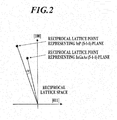
- the angle formed between the (5-1-1) plane of the InGaAs photo-absorption layer 14 and the (5-1-1) plane of the InP substrate 11 is now represented by angle ⁇ in the reciprocal lattice space illustrated in FIG. 2 .
- the angle is calculated by a coordinate of reciprocal lattice point representing the (5-1-1) plane of the InP substrate 1 reciprocal lattice point, and a coordinate of reciprocal lattice point representing the (5-1-1) plane of the InGaAs photo-absorption layer 14.
- the semiconductor epitaxial substrates 1 illustrated in FIG. 1 were manufactured respectively using off-angle InP substrates 11 (lattice constant: 5.8688 ⁇ ) having principal surfaces inclined from the (100) plane by 1°, 2°, 3° and 5° into the [110] direction, and the semiconductor layers 12 to 15 with lattice distortion were epitaxially grown in sequence by MOCVD on the InP substrates 11.
- Source materials of the semiconductor layers 12 to 15 were AsH 3 , PH 3 , TMIn and TMGa, used under a growth pressure of 50 Torr, at a growth temperature 600 to 670°C.
- the graded buffer layer 12 composed of a plurality of InAs x P 1-x layers was grown on the InP substrate 11.
- the compositional ratio x of As was adjusted so as to gradually increase the lattice constant. More specifically, by adjusting the compositional ratio x of As to 0.05 to 0.60, the lattice constant of the graded buffer layer 12 was adjusted so as to increase stepwise in the range from 5.8688 ⁇ which is the lattice constant of the InP substrate 11 (first lattice constant), to 5.9852 ⁇ which is the lattice constant of the InGaAs photo-absorption layer 14 (second lattice constant).
- the InAs x P 1-x buffer layer 13 (lattice constant: 5.9880 ⁇ ) having a compositional ratio x of As of approximately 0.6
- the In y Ga 1-y As photo-absorption layer 14 (lattice constant: 5.9852 ⁇ ) having a compositional ratio y of In of approximately 0.82
- the InAs x P 1-x window layer 15 having a compositional ratio x of As of approximately 0.6 were grown in sequence on the graded buffer layer 12, to thereby manufacture the semiconductor epitaxial substrate 1.
- the InAsP graded buffer layer 12 was approximately 0.3 to 1 ⁇ m thick, the InAsP buffer layer 13 was approximately 0.5 to 5 ⁇ m thick, the InGaAs photo-absorption layer 14 was 1 to 5 ⁇ m thick, and the InAsP window layer 15 was 0.5 to 3 ⁇ m thick.
- the semiconductor epitaxial substrates 1 illustrated in FIG. 1 were manufactured respectively using off-angle InP substrates 11 (lattice constant: 5.8688 ⁇ ) having principal surfaces inclined from the (100) plane by 0° and 0.5° into the [110] direction, and the semiconductor layers 12 to 15 having lattice distortion were epitaxially grown in sequence by MOCVD on each of the InP substrates 11. Specific conditions of the growth were same as those in Example.
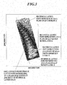
- FIG. 3 is a drawing illustrating an exemplary reciprocal lattice map of the (5-1-1) plane of the semiconductor epitaxial substrate 1 manufactured in Example
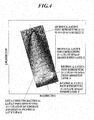
- FIG. 4 is a drawing illustrating an exemplary reciprocal lattice map of the (5-1-1) plane of the semiconductor epitaxial substrate 1 manufactured in Comparative Example.
- FIG. 3 illustrates the reciprocal map of the semiconductor epitaxial substrate 1 having the semiconductor layers 12 to 15 epitaxially grown on the 2° off-angle InP substrate 11
- FIG. 4 illustrates the reciprocal map of the semiconductor epitaxial substrate 1 having the semiconductor layers 12 to 15 epitaxially grown on the 0° off-angle InP substrate 11.
- FIGs. 3 illustrates the reciprocal map of the semiconductor epitaxial substrate 1 having the semiconductor layers 12 to 15 epitaxially grown on the 2° off-angle InP substrate 11
- FIG. 4 illustrates the reciprocal map of the semiconductor epitaxial substrate 1 having the semiconductor layers 12 to 15 epitaxially grown on the 0° off-angle InP substrate 11.
- reciprocal lattice vector of the (011) plane is aligned to the direction of X-axis
- reciprocal lattice vector of the (100) plane is aligned to the direction of Y-axis, with the same scales for easy comparison of broadening of the reciprocal lattice point.
- plane spacing of crystal planes and crystal orientation may be determined based on coordinate of the reciprocal lattice point (size of reciprocal lattice vector), and angle formed between different crystal planes may be determined based on coordinates of reciprocal lattice points representing the crystal planes.
- Degree of crystallinity is also known, since a sample with a poor crystallinity will give a large degree of broadening of the reciprocal lattice points.
- the coordinate of the reciprocal lattice point gives plane spacing of the (500) plane which is the direction of crystal growth (direction of the normal line on the substrate), plane spacing of the (0-1-1) planes which lie in parallel with the substrate, and angle between the (500) plane and the (0-1-1) plane. From the information including the plane spacing, it is now possible to estimate the degree of lattice relaxation of the grown crystal.
- a defect-free ideal crystal will give a reciprocal lattice map showing a circular spot pattern without broadening of the reciprocal lattice point, whereas a mosaic structure which is an assemblage of micro-crystals slightly differing in the direction of orientation will give the reciprocal lattice vectors slightly differing in the direction, and will therefore give a reciprocal lattice map showing an elliptic pattern with a large degree of broadening of the reciprocal lattice point.
- the semiconductor epitaxial substrate 1 manufactured in the Example showed a smaller degree of broadening of the reciprocal lattice points in the direction of long axis (lateral direction) as compared with the semiconductor epitaxial substrate 1 manufactured in Comparative Example, proving the improved crystallinity (reduced mosaicity).
- the semiconductor epitaxial substrates 1 manufactured in Example respectively by using the InP substrates 11 with off-angles of 1°, 3° and 5° gave similar results with FIG. 3 , by which a mosaicity was improved.
- the semiconductor epitaxial substrate 1 manufactured in Comparative Example by using the InP substrate 11 with an off-angle of 0.5° was found to give a similar result with FIG. 4 , indicating deteriorated mosaicity.
- the crystal grows anyhow up to a critical thickness of the semiconductor layer while deforming the lattice, and upon exceeding the critical thickness, the crystal produces crystal defects and so forth to relax the strain energy.
- the semiconductor layers grown on the growth substrate with an off-angle of 0°, such as in Comparative Example will produce the micro-domains having the plane direction oriented to all directions, since every direction is energetically equivalent for the crystals in the micro-domains to be aligned, showing a broadened reciprocal lattice point as seen in FIG. 4 .
- the semiconductor epitaxial substrate 1 of Comparative Example shows the individual reciprocal lattice points representing the (5-1-1) planes of the semiconductor layers 12 to 15 fallen on line L which connects the reciprocal lattice point representing the (5-1-1) plane of the InP substrate 11 and the origin of the reciprocal lattice space (see FIG. 4 )
- the semiconductor epitaxial substrate 1 of Example shows the individual reciprocal lattice points representing the (5-1-1) planes of the semiconductor layers 12 to 15 fallen slightly away from line L (see FIG. 3 ).
- FIG. 5 is a drawing illustrating relation of the angle ⁇ of the (5-1-1) plane of the InGaAs photo-absorption layer 14 away from the (5-1-1) plane of the InP substrate 11, with half-value width of reciprocal lattice point of the InGaAs photo-absorption layer 14, in the semiconductor epitaxial substrates 1 manufactured in Example and Comparative Example.
- the half-value width reduces as the angle ⁇ increases.
- the half-value width is smaller than 1.5 ⁇ 10 -3 a.u. if the angle ⁇ is set to 0.05° or larger, proving an extremely good crystallinity.
- FIG. 6 is a drawing illustrating relation of the angle ⁇ of the (5-1-1) plane of the InGaAs photo-absorption layer 14 away from the (5-1-1) plane of the InP substrate 11, with PL intensity which indicates optical quality.
- the PL intensity increases by 20 to 30% when the angle ⁇ is set to 0.05° or larger, as compared with the case with an angle ⁇ of 0.05° or smaller, proving formation of high-quality semiconductor layers also from the viewpoint of optical quality.
- the InGaAs photo-absorption layer 14 grows while being aligned in a constant direction, to thereby give a high-quality crystal with only a small mosaicity. Accordingly, by using the semiconductor epitaxial substrate 1, performances of semiconductor devices such as infrared sensors may be improved.
- the angle between the (5-1-1) plane of the InGaAs photo-absorption layer 14 and the (5-1-1) plane of the InP substrate 11 is most largely affected by the off-angle of the InP substrate 11, but not solely.
- Use of the off-angle substrate as the growth substrate is merely one technique of adjusting the angle between the (5-1-1) plane of the InGaAs photo-absorption layer 14 and the (5-1-1) plane of the InP substrate 11 to 0.05° or larger, and use of the InP substrate 11 having an off-angle of 1° or larger, for example, is supposed to be preferable.
- the present invention is not limited thereto, and may be modified without departing from the spirit thereof.
- the embodiment described in the above dealt with the case where the InGaAs layer 14 was grown over the InP substrate 11, while placing the InAsP graded buffer layer 12 and the InAsP buffer layer 13 in between, the present invention is also applicable to a semiconductor epitaxial substrate which includes, epitaxially grown on a semiconductor substrate having a first lattice constant, a graded buffer layer which is compositionally graded so as to increase the lattice constant stepwise in the range from the first lattice constant to a second lattice constant larger than the first lattice constant; and a semiconductor layer which is composed of a semiconductor crystal having the second lattice constant.
- the present invention is applicable to a semiconductor epitaxial substrate which includes, grown on a Si substrate, a Si x Ge 1-x graded buffer layer and a Si x Ge 1-x layer which have the lattice constant larger than that of Si, or a semiconductor epitaxial substrate which includes, grown on a GaAs substrate, an In x Al 1-x As compositionally graded buffer layer and an In x Al 1-x As layer which have the lattice constant larger than that of Ga.
Landscapes
- Light Receiving Elements (AREA)
- Crystals, And After-Treatments Of Crystals (AREA)
Abstract
Description
- The present invention relates to a semiconductor epitaxial substrate having a semiconductor layer which has a lattice constant different from that of the growth substrate, and is epitaxially grown on a growth substrate while placing a graded buffer layer in between.
- A semiconductor epitaxial substrate configured by an InP substrate which is used as a growth substrate, and a photo-absorption layer which is composed of InGaAs crystal grown on the InP substrate and has the lattice constant (5.8688 Ǻ) equal to that of the InP substrate, has been used for infrared sensors having sensitivities up to 1.7 µm or around. This sort of semiconductor epitaxial substrate is manufactured, for example, by epitaxial growth process such as metal organic chemical vapor deposition (MOCVD) and hydride vapor phase epitaxy (HVPE).
- On the other hand, near-infrared sensors having sensitivities in longer wavelength ranges of approximately 1.9 to 2.6 µm need a photo-absorption layer composed of InGaAs which has a lattice constant larger than that of the InP substrate (5.87 to 6.00 Ǻ, for example) . When the semiconductor layer having the lattice constant different from that of the growth substrate is grown thereon as the photo-absorption layer, lattice defect such as misfit dislocation occurs at the interface between the growth substrate and the semiconductor layer, and the lattice defect also propagates into the semiconductor layer. A high density of lattice defect in the photo-absorption layer considerably degrades performances of the near-infrared sensor.
Accordingly, for the case where the InGaAs having the lattice constant larger than that of the InP substrate is used as the photo-absorption layer, one known technique is such as providing, between the InP substrate and the InGaAs photo-absorption layer, a graded buffer layer (such as InAsxP1-x (0≤x≤1)) having the lattice constant which increases stepwise from the lattice constant of the InP substrate to the lattice constant of the InGaAs photo-absorption layer, to thereby prevent the lattice defect from propagating towards the InGaAs photo-absorption layer (seePatent Documents 1 and 2, for example).
Another general method is such as growing the semiconductor layer epitaxially on an off-angle growth substrate which has an inclined (by 2 degrees, for example) principal surface (see Non-PatentDocument 1, for example). -
- Patent Document 1: Japanese Examined Patent Publication No.
3285981 - Patent Document 2: Japanese Laid-Open Patent Publication No.
2004-319765 -
- Non-Patent Document 1: M.A. di Forte-Poisson et al., J. Cryst. Growth, 124 (1992), 782
- In the process of epitaxial growth of the semiconductor layer (InGaAs photo-absorption layer, for example) by MOCVD, a growth substrate generally used has the (100) surface. However, the graded buffer layer, which has the lattice constant larger than that of the growth substrate and is grown thereon, was found to have a lot of micro-domains formed in the grown crystal, each having direction of crystal axis slightly different from that of the growth substrate, to thereby give a mosaic structure composed of an assemblage of the micro-domains. Generation of such mosaic structure may result in increase in lattice defect in the crystal, and may degrade quality of the compound semiconductor crystal.
- It is therefore an object of the present invention to provide a semiconductor epitaxial substrate having a semiconductor layer which has the lattice constant different from that of the growth substrate, epitaxially grown on the growth substrate while placing a graded buffer layer in between, featured by a small mosaicity of the semiconductor layer, and is suitable for manufacturing of semiconductor devices.
- The invention described in
Claim 1 is conceived in order to achieve the object described in the above. According to the invention, there is provided a semiconductor epitaxial substrate which includes: - a semiconductor substrate having a first lattice constant;
- a graded buffer layer which is compositionally graded so as to increase the lattice constant stepwise in the range from the first lattice constant to a second lattice constant larger than the first lattice constant and epitaxially grown on the semiconductor substrate; and
- a semiconductor layer which is composed of a semiconductor crystal having the second lattice constant and epitaxially grown on the graded buffer layer, wherein
- the angle between the (mnn) plane (where, m and n are integers except m=n=0) of the semiconductor layer and the (mnn) plane of the semiconductor substrate is +0.05° or larger, when the clockwise direction of rotation from the [100] direction to the [011] direction is positive.
- According to the invention described in Claim 2, there is provided the semiconductor epitaxial substrate of
Claim 1, wherein
the semiconductor substrate is composed of InP;
the graded buffer layer is composed of InAsP; and
the semiconductor layer is composed of InGaAs. - According to the semiconductor epitaxial substrate of the present invention, since the semiconductor layer has a small mosaicity and has an extremely high crystallinity, so that performances of semiconductor devices such as infrared sensor may be improved to a considerable degree.
-
- [
FIG. 1 ] It is a drawing illustrating a multi-layered structure of a semiconductor epitaxial substrate according to one embodiment. - [
FIG. 2 ] It is a drawing illustrating an angle of inclination α of the (5-1-1) plane of an InGaAs photo-absorption layer away from the (5-1-1) plane of anInP substrate 11, expressed in a reciprocal lattice space. - [
FIG. 3 ] It is a drawing illustrating a reciprocal lattice map of a semiconductorepitaxial substrate 1 which has a 2° off-angle InP substrate 11 andsemiconductor layers 12 to 15 epitaxially grown thereon. - [
FIG. 4 ] It is a drawing illustrating a reciprocal lattice map of a semiconductorepitaxial substrate 1 composed of a 0° off-angle InP substrate 11 andsemiconductor layers 12 to 15 epitaxially grown thereon. - [
FIG. 5 ] It is a drawing illustrating relation of the angle α of the (5-1-1) plane of the InGaAs photo-absorption layer away from the (5-1-1) plane of the InP substrate, with half-value width of reciprocal lattice point of the InGaAs photo-absorption layer. - [
FIG. 6 ] It is a drawing illustrating relation of the angle α of the (5-1-1) plane of the InGaAs photo-absorption layer away from the (5-1-1) plane of the InP substrate, with PL (photoluminescence) intensity which indicates optical quality. - Embodiments of the present invention will be explained below, referring to the attached drawings.
FIG. 1 is a drawing illustrating a multi-layered structure of a semiconductor epitaxial substrate of the present invention applied to a photodiode.
As illustrated inFIG. 1 , an semiconductorepitaxial substrate 1 of the embodiment has a multi-layered structure having, stacked in sequence on anInP substrate 11, an InAsP gradedbuffer layer 12, anInAsP buffer layer 13, an InGaAs photo-absorption layer 14, and anInAsP window layer 15. - The angle α of the (5-1-1) plane of the InGaAs photo-
absorption layer 14 away from the (5-1-1) plane of theInP substrate 11 is set to +0.05° or larger, assuming the clockwise direction of rotation from the [100] direction to the [011] direction as positive. In the following description, the angle formed between the (5-1-1) plane of the InGaAs photo-absorption layer 14 and the (5-1-1) plane of theInP substrate 11 will be depicted similarly, always assuming the clockwise direction of rotation from the [100] direction to the [011] direction as positive.
The angle formed between the (5-1-1) plane of the InGaAs photo-absorption layer 14 and the (5-1-1) plane of theInP substrate 11 is now represented by angle α in the reciprocal lattice space illustrated inFIG. 2 . In other words, the angle is calculated by a coordinate of reciprocal lattice point representing the (5-1-1) plane of theInP substrate 1 reciprocal lattice point, and a coordinate of reciprocal lattice point representing the (5-1-1) plane of the InGaAs photo-absorption layer 14. - In Example, the semiconductor
epitaxial substrates 1 illustrated inFIG. 1 were manufactured respectively using off-angle InP substrates 11 (lattice constant: 5.8688 Ǻ) having principal surfaces inclined from the (100) plane by 1°, 2°, 3° and 5° into the [110] direction, and thesemiconductor layers 12 to 15 with lattice distortion were epitaxially grown in sequence by MOCVD on theInP substrates 11. Source materials of thesemiconductor layers 12 to 15 were AsH3, PH3, TMIn and TMGa, used under a growth pressure of 50 Torr, at a growth temperature 600 to 670°C. - First, the graded
buffer layer 12 composed of a plurality of InAsxP1-x layers was grown on theInP substrate 11. The compositional ratio x of As was adjusted so as to gradually increase the lattice constant. More specifically, by adjusting the compositional ratio x of As to 0.05 to 0.60, the lattice constant of the gradedbuffer layer 12 was adjusted so as to increase stepwise in the range from 5.8688 Ǻ which is the lattice constant of the InP substrate 11 (first lattice constant), to 5.9852 Ǻ which is the lattice constant of the InGaAs photo-absorption layer 14 (second lattice constant).
Then, the InAsxP1-x buffer layer 13 (lattice constant: 5.9880 Ǻ) having a compositional ratio x of As of approximately 0.6, the InyGa1-yAs photo-absorption layer 14 (lattice constant: 5.9852 Ǻ) having a compositional ratio y of In of approximately 0.82, and the InAsxP1-x window layer 15 having a compositional ratio x of As of approximately 0.6 were grown in sequence on the gradedbuffer layer 12, to thereby manufacture the semiconductorepitaxial substrate 1.
The InAsP gradedbuffer layer 12 was approximately 0.3 to 1 µm thick, theInAsP buffer layer 13 was approximately 0.5 to 5 µm thick, the InGaAs photo-absorption layer 14 was 1 to 5 µm thick, and theInAsP window layer 15 was 0.5 to 3 µm thick. - In Comparative Example, the semiconductor
epitaxial substrates 1 illustrated inFIG. 1 were manufactured respectively using off-angle InP substrates 11 (lattice constant: 5.8688 Ǻ) having principal surfaces inclined from the (100) plane by 0° and 0.5° into the [110] direction, and thesemiconductor layers 12 to 15 having lattice distortion were epitaxially grown in sequence by MOCVD on each of theInP substrates 11. Specific conditions of the growth were same as those in Example. -
FIG. 3 is a drawing illustrating an exemplary reciprocal lattice map of the (5-1-1) plane of the semiconductorepitaxial substrate 1 manufactured in Example, andFIG. 4 is a drawing illustrating an exemplary reciprocal lattice map of the (5-1-1) plane of the semiconductorepitaxial substrate 1 manufactured in Comparative Example.
FIG. 3 illustrates the reciprocal map of the semiconductorepitaxial substrate 1 having thesemiconductor layers 12 to 15 epitaxially grown on the 2° off-angle InP substrate 11, andFIG. 4 illustrates the reciprocal map of the semiconductorepitaxial substrate 1 having thesemiconductor layers 12 to 15 epitaxially grown on the 0° off-angle InP substrate 11. InFIGs. 3 and4 , reciprocal lattice vector of the (011) plane is aligned to the direction of X-axis, reciprocal lattice vector of the (100) plane is aligned to the direction of Y-axis, with the same scales for easy comparison of broadening of the reciprocal lattice point. - According to reciprocal lattice mapping, plane spacing of crystal planes and crystal orientation may be determined based on coordinate of the reciprocal lattice point (size of reciprocal lattice vector), and angle formed between different crystal planes may be determined based on coordinates of reciprocal lattice points representing the crystal planes. Degree of crystallinity is also known, since a sample with a poor crystallinity will give a large degree of broadening of the reciprocal lattice points.
- In an exemplary reciprocal lattice mapping of the asymmetrical (5-1-1) plane of the semiconductor epitaxial substrate, the coordinate of the reciprocal lattice point gives plane spacing of the (500) plane which is the direction of crystal growth (direction of the normal line on the substrate), plane spacing of the (0-1-1) planes which lie in parallel with the substrate, and angle between the (500) plane and the (0-1-1) plane. From the information including the plane spacing, it is now possible to estimate the degree of lattice relaxation of the grown crystal.
A defect-free ideal crystal will give a reciprocal lattice map showing a circular spot pattern without broadening of the reciprocal lattice point, whereas a mosaic structure which is an assemblage of micro-crystals slightly differing in the direction of orientation will give the reciprocal lattice vectors slightly differing in the direction, and will therefore give a reciprocal lattice map showing an elliptic pattern with a large degree of broadening of the reciprocal lattice point. - It is clearly understood from
FIGs. 3 and4 , that thesemiconductor epitaxial substrate 1 manufactured in the Example showed a smaller degree of broadening of the reciprocal lattice points in the direction of long axis (lateral direction) as compared with thesemiconductor epitaxial substrate 1 manufactured in Comparative Example, proving the improved crystallinity (reduced mosaicity).
Although not illustrated herein, also thesemiconductor epitaxial substrates 1 manufactured in Example respectively by using theInP substrates 11 with off-angles of 1°, 3° and 5°, gave similar results withFIG. 3 , by which a mosaicity was improved. In contrast, thesemiconductor epitaxial substrate 1 manufactured in Comparative Example by using theInP substrate 11 with an off-angle of 0.5°, was found to give a similar result withFIG. 4 , indicating deteriorated mosaicity. - This indicates that, when the semiconductor layer (InGaAs photo-absorption layer 14) having the lattice constant larger than that of the growth substrate (InP substrate 11) is grown on the growth substrate, use of a growth substrate with a small off-angle (0° or 0.5°, for example) may induce a mosaic structure having multi-directional crystal orientation in the micro-domains in the grown crystal. On the other hand, use of a growth substrate having an off-angle of certain level or larger (1° or larger, for example) may induce a constant orientation of the grown crystal relative to the growth substrate.
- More specifically, when the semiconductor layer having the lattice constant larger than that of the growth substrate is grown on the growth substrate, the crystal grows anyhow up to a critical thickness of the semiconductor layer while deforming the lattice, and upon exceeding the critical thickness, the crystal produces crystal defects and so forth to relax the strain energy.
In this process, the semiconductor layers grown on the growth substrate with an off-angle of 0°, such as in Comparative Example, will produce the micro-domains having the plane direction oriented to all directions, since every direction is energetically equivalent for the crystals in the micro-domains to be aligned, showing a broadened reciprocal lattice point as seen inFIG. 4 .
On the other hand, when the growth substrate having an off-angle of 2° was used as in Example, the broadening of the reciprocal lattice point will reduce as seen inFIG. 3 . In short, it is understood that the use of the growth substrate with an off-angle of 2° allows the growth in a constant direction, whereas the use of the growth substrate with an off-angle of 0° results in the mosaic structure due to growth of crystal in all directions. - What is worthy of mention is that, while the
semiconductor epitaxial substrate 1 of Comparative Example shows the individual reciprocal lattice points representing the (5-1-1) planes of the semiconductor layers 12 to 15 fallen on line L which connects the reciprocal lattice point representing the (5-1-1) plane of theInP substrate 11 and the origin of the reciprocal lattice space (seeFIG. 4 ), whereas thesemiconductor epitaxial substrate 1 of Example shows the individual reciprocal lattice points representing the (5-1-1) planes of the semiconductor layers 12 to 15 fallen slightly away from line L (seeFIG. 3 ).
Our analytical study revealed that thesemiconductor epitaxial substrate 1 of Comparative Example showed an angle between the (5-1-1) plane of the InGaAs photo-absorption layer 14 and the (5-1-1) plane of theInP substrate 11 of -0.07 to +0.03°, whereas thesemiconductor epitaxial substrate 1 of Example showed the angle of +0.05 to +0.72°. -
FIG. 5 is a drawing illustrating relation of the angle α of the (5-1-1) plane of the InGaAs photo-absorption layer 14 away from the (5-1-1) plane of theInP substrate 11, with half-value width of reciprocal lattice point of the InGaAs photo-absorption layer 14, in thesemiconductor epitaxial substrates 1 manufactured in Example and Comparative Example.
As illustrated inFIG. 5 , the half-value width reduces as the angle α increases. In particular, the half-value width is smaller than 1.5×10⁻³ a.u. if the angle α is set to 0.05° or larger, proving an extremely good crystallinity. -
FIG. 6 is a drawing illustrating relation of the angle α of the (5-1-1) plane of the InGaAs photo-absorption layer 14 away from the (5-1-1) plane of theInP substrate 11, with PL intensity which indicates optical quality.
As illustrated inFIG. 6 , the PL intensity increases by 20 to 30% when the angle α is set to 0.05° or larger, as compared with the case with an angle α of 0.05° or smaller, proving formation of high-quality semiconductor layers also from the viewpoint of optical quality. - In short, it is understood that, in the semiconductor epitaxial substrate having an angle between the (5-1-1) plane of the InGaAs photo-
absorption layer 14 and the (5-1-1) plane of theInP substrate 11 of +0.05° or larger, assuming the clockwise direction of rotation from the [100] direction to the [011] direction as positive, the InGaAs photo-absorption layer 14 grows while being aligned in a constant direction, to thereby give a high-quality crystal with only a small mosaicity. Accordingly, by using thesemiconductor epitaxial substrate 1, performances of semiconductor devices such as infrared sensors may be improved. - Note that the angle between the (5-1-1) plane of the InGaAs photo-
absorption layer 14 and the (5-1-1) plane of theInP substrate 11 is most largely affected by the off-angle of theInP substrate 11, but not solely. Use of the off-angle substrate as the growth substrate is merely one technique of adjusting the angle between the (5-1-1) plane of the InGaAs photo-absorption layer 14 and the (5-1-1) plane of theInP substrate 11 to 0.05° or larger, and use of theInP substrate 11 having an off-angle of 1° or larger, for example, is supposed to be preferable. - Having described the present invention conceived by the present inventors referring to the specific embodiment, the present invention is not limited thereto, and may be modified without departing from the spirit thereof.
The embodiment described in the above dealt with the case where theInGaAs layer 14 was grown over theInP substrate 11, while placing the InAsP gradedbuffer layer 12 and theInAsP buffer layer 13 in between, the present invention is also applicable to a semiconductor epitaxial substrate which includes, epitaxially grown on a semiconductor substrate having a first lattice constant, a graded buffer layer which is compositionally graded so as to increase the lattice constant stepwise in the range from the first lattice constant to a second lattice constant larger than the first lattice constant; and a semiconductor layer which is composed of a semiconductor crystal having the second lattice constant.
For example, the present invention is applicable to a semiconductor epitaxial substrate which includes, grown on a Si substrate, a SixGe1-x graded buffer layer and a SixGe1-x layer which have the lattice constant larger than that of Si, or a semiconductor epitaxial substrate which includes, grown on a GaAs substrate, an InxAl1-xAs compositionally graded buffer layer and an InxAl1-xAs layer which have the lattice constant larger than that of Ga. - The embodiment described in the above dealt with the case where the angle between the (5-1-1) plane of the InGaAs photo-
absorption layer 14 and the (5-1-1) plane of theInP substrate 11 is 0.05° or larger, our crystallographic investigations also revealed that the same will apply to the asymmetric (mnn) planes (m and n are integers, where 0≤m, n≤7, except m=n=0), such as the (311) plane, the (511) plane, and the (711) plane.
In short, the semiconductor epitaxial substrate of the present invention characteristically has an angle, between the (mnn) plane (where, m and n are integers except m=n=0) of the semiconductor layer and the (mnn) plane of the semiconductor substrate, of +0.05° or larger, assuming the clockwise direction of rotation from the [100] direction to the [011] direction as positive. - It is to be understood that the embodiment disclosed in the above is illustrative but not restrictive in all aspects. The scope of the present invention is to be determined solely by the claims rather than by the description, so that all changes that fall within metes and bounds of the claims, or equivalence thereof are therefore intended to be embraced therein.
-
- 1 semiconductor epitaxial substrate
- 11 InP substrate (semiconductor substrate with first lattice constant)
- 12 InAsP graded buffer layer
- 13 InAsP buffer layer
- 14 InGaAs photo-absorption layer (semiconductor layer with second lattice constant)
- 15 InAsP window layer
Claims (2)
- A semiconductor epitaxial substrate comprising:a semiconductor substrate having a first lattice constant;a graded buffer layer which is compositionally graded so as to increase the lattice constant stepwise in the range from the first lattice constant to a second lattice constant larger than the first lattice constant and epitaxially grown on the semiconductor substrate; anda semiconductor layer which is composed of a semiconductor crystal having the second lattice constant and epitaxially grown on the graded buffer layer, whereinthe angle between the (mnn) plane (where, m and n are integers except m=n=0) of the semiconductor layer and the (mnn) plane of the semiconductor substrate is +0.05° or larger, when the clockwise direction of rotation from the [100] direction to the [011] direction is positive.
- The semiconductor epitaxial substrate of Claim 1,
wherein
the semiconductor substrate is composed of InP;
the graded buffer layer is composed of InAsP; and
the semiconductor layer is composed of InGaAs.
Applications Claiming Priority (2)
| Application Number | Priority Date | Filing Date | Title |
|---|---|---|---|
| JP2010044819 | 2010-03-02 | ||
| PCT/JP2011/054581 WO2011108519A1 (en) | 2010-03-02 | 2011-03-01 | Semiconductor epitaxial substrate |
Publications (2)
| Publication Number | Publication Date |
|---|---|
| EP2543754A1 true EP2543754A1 (en) | 2013-01-09 |
| EP2543754A4 EP2543754A4 (en) | 2015-03-25 |
Family
ID=44542170
Family Applications (1)
| Application Number | Title | Priority Date | Filing Date |
|---|---|---|---|
| EP11750629.5A Ceased EP2543754A4 (en) | 2010-03-02 | 2011-03-01 | EPITACTIC SEMICONDUCTOR SUBSTRATE |
Country Status (6)
| Country | Link |
|---|---|
| US (1) | US20130001645A1 (en) |
| EP (1) | EP2543754A4 (en) |
| JP (1) | JP5859423B2 (en) |
| CN (1) | CN102782195A (en) |
| TW (1) | TWI529965B (en) |
| WO (1) | WO2011108519A1 (en) |
Families Citing this family (2)
| Publication number | Priority date | Publication date | Assignee | Title |
|---|---|---|---|---|
| CN105308720B (en) * | 2013-06-11 | 2017-10-20 | 欧司朗光电半导体有限公司 | Method for manufacturing nitride compound semiconductor device |
| US9842900B2 (en) | 2016-03-30 | 2017-12-12 | International Business Machines Corporation | Graded buffer layers with lattice matched epitaxial oxide interlayers |
Family Cites Families (8)
| Publication number | Priority date | Publication date | Assignee | Title |
|---|---|---|---|---|
| US4117504A (en) * | 1976-08-06 | 1978-09-26 | Vadim Nikolaevich Maslov | Heterogeneous semiconductor structure with composition gradient and method for producing same |
| JP3285981B2 (en) | 1993-01-14 | 2002-05-27 | 浜松ホトニクス株式会社 | Semiconductor light receiving element |
| US5387796A (en) * | 1993-05-26 | 1995-02-07 | Epitaxx, Inc. | Low leakage current photodetector arrays |
| US6482672B1 (en) * | 1997-11-06 | 2002-11-19 | Essential Research, Inc. | Using a critical composition grading technique to deposit InGaAs epitaxial layers on InP substrates |
| US20060048700A1 (en) * | 2002-09-05 | 2006-03-09 | Wanlass Mark W | Method for achieving device-quality, lattice-mismatched, heteroepitaxial active layers |
| JP2004319765A (en) | 2003-04-16 | 2004-11-11 | Sumitomo Electric Ind Ltd | Compound semiconductor wafer and method of manufacturing the same |
| JP2006080448A (en) * | 2004-09-13 | 2006-03-23 | Sumitomo Electric Ind Ltd | Epitaxial wafer and device |
| WO2006030565A1 (en) * | 2004-09-17 | 2006-03-23 | Nippon Mining & Metals Co., Ltd. | Epitaxial crystal growing method |
-
2011
- 2011-03-01 WO PCT/JP2011/054581 patent/WO2011108519A1/en not_active Ceased
- 2011-03-01 JP JP2012503176A patent/JP5859423B2/en not_active Expired - Fee Related
- 2011-03-01 CN CN201180011758XA patent/CN102782195A/en active Pending
- 2011-03-01 EP EP11750629.5A patent/EP2543754A4/en not_active Ceased
- 2011-03-01 US US13/582,365 patent/US20130001645A1/en not_active Abandoned
- 2011-03-02 TW TW100106895A patent/TWI529965B/en not_active IP Right Cessation
Non-Patent Citations (4)
| Title |
|---|
| DASHIELL M W ET AL: "Triple-axis X-ray reciprocal space mapping of InyGa1-yAs thermophotovoltaic diodes grown on (100) InP substrates", SOLAR ENERGY MATERIALS AND SOLAR CELLS, ELSEVIER SCIENCE PUBLISHERS, AMSTERDAM, NL, vol. 92, no. 9, 2 June 2008 (2008-06-02), pages 1003-1010, XP022735440, ISSN: 0927-0248, DOI: 10.1016/J.SOLMAT.2008.02.042 [retrieved on 2008-06-02] * |
| ELDREDGE J W ET AL: "EFFECT OF SUBSTRATE MISCUT ON THE STRUCTURAL PROPERTIES OF INGAAS LINEAR GRADED BUFFER LAYERS GROWN BY MOLECULAR-BEAM EPITAXY ON GAAS", JOURNAL OF VACUUM SCIENCE AND TECHNOLOGY: PART B, AVS / AIP, MELVILLE, NEW YORK, NY, US, vol. 13, no. 2, March 1995 (1995-03), pages 689-691, XP000651229, ISSN: 1071-1023, DOI: 10.1116/1.588136 * |
| HUDAIT MANTU ET AL: "Strain relaxation properties of InAsyP1-y metamorphic materials grown on InP substrates", JOURNAL OF APPLIED PHYSICS, AMERICAN INSTITUTE OF PHYSICS, US, vol. 105, no. 6, 25 March 2009 (2009-03-25), pages 61643-61643, XP012120087, ISSN: 0021-8979, DOI: 10.1063/1.3098232 * |
| See also references of WO2011108519A1 * |
Also Published As
| Publication number | Publication date |
|---|---|
| TW201205870A (en) | 2012-02-01 |
| JP5859423B2 (en) | 2016-02-10 |
| CN102782195A (en) | 2012-11-14 |
| TWI529965B (en) | 2016-04-11 |
| JPWO2011108519A1 (en) | 2013-06-27 |
| EP2543754A4 (en) | 2015-03-25 |
| US20130001645A1 (en) | 2013-01-03 |
| WO2011108519A1 (en) | 2011-09-09 |
Similar Documents
| Publication | Publication Date | Title |
|---|---|---|
| US9142723B2 (en) | Semiconductor wafer comprising gallium nitride layer having one or more silicon nitride interlayer therein | |
| US8680581B2 (en) | Method for producing group III nitride semiconductor and template substrate | |
| US7253499B2 (en) | III-V group nitride system semiconductor self-standing substrate, method of making the same and III-V group nitride system semiconductor wafer | |
| US20140291694A1 (en) | Planar nonpolar group-iii nitride films grown on miscut substrates | |
| KR20110099103A (en) | Method for manufacturing nitride compound semiconductor substrate and nitride compound semiconductor independent substrate | |
| CN116259531B (en) | Sphalerite III nitrides | |
| KR20110018890A (en) | Group III nitride templates and related heterostructures, devices, and methods of making them | |
| CN103367113B (en) | The manufacture method of group III nitride semiconductor and group III nitride semiconductor | |
| EP2904630B1 (en) | Semiconductor material | |
| JP5647997B2 (en) | Epitaxial crystal substrate manufacturing method, epitaxial crystal substrate, and semiconductor device manufactured using the same | |
| Imura et al. | Flat (1120) GaN thin film on precisely offset-controlled (1102) sapphire substrate | |
| EP2634294A1 (en) | Method for manufacturing optical element | |
| EP2543754A1 (en) | Semiconductor epitaxial substrate | |
| Araki et al. | Effect of misorientation angle of r-plane sapphire substrate on a-plane GaN grown by metalorganic vapor phase epitaxy | |
| Kim et al. | Reduction in crystallographic tilting of lateral epitaxial overgrown GaN by removal of oxide mask | |
| US9525101B2 (en) | Optoelectronic device | |
| EP3050075A1 (en) | A semiconductor wafer and a method for producing the semiconductor wafer | |
| KR101660734B1 (en) | method for growing nitride semiconductor film | |
| JP2007180270A (en) | Method for manufacturing compound semiconductor epitaxial substrate | |
| CN104124315A (en) | Optoelectronic component | |
| Han et al. | Nonpolar a-plane ZnO films grown on GaN/sapphire templates with SiN x interlayer by pulsed laser deposition | |
| JP2011140428A (en) | Method for manufacturing nitride-based compound semiconductor substrate, and nitride-based compound semiconductor self-standing substrate | |
| Han | Growth of gallium nitride layers with very low threading dislocation densities |
Legal Events
| Date | Code | Title | Description |
|---|---|---|---|
| PUAI | Public reference made under article 153(3) epc to a published international application that has entered the european phase |
Free format text: ORIGINAL CODE: 0009012 |
|
| 17P | Request for examination filed |
Effective date: 20120928 |
|
| AK | Designated contracting states |
Kind code of ref document: A1 Designated state(s): AL AT BE BG CH CY CZ DE DK EE ES FI FR GB GR HR HU IE IS IT LI LT LU LV MC MK MT NL NO PL PT RO RS SE SI SK SM TR |
|
| RIN1 | Information on inventor provided before grant (corrected) |
Inventor name: KAKUTA, KOJI Inventor name: KANAI, SUSUMU Inventor name: NOZAKI, TATSUYA |
|
| DAX | Request for extension of the european patent (deleted) | ||
| A4 | Supplementary search report drawn up and despatched |
Effective date: 20150223 |
|
| RIC1 | Information provided on ipc code assigned before grant |
Ipc: C30B 25/18 20060101ALI20150217BHEP Ipc: H01L 21/205 20060101ALI20150217BHEP Ipc: C30B 29/40 20060101AFI20150217BHEP Ipc: H01L 21/02 20060101ALI20150217BHEP Ipc: C23C 16/30 20060101ALI20150217BHEP |
|
| 17Q | First examination report despatched |
Effective date: 20160126 |
|
| REG | Reference to a national code |
Ref country code: DE Ref legal event code: R003 |
|
| STAA | Information on the status of an ep patent application or granted ep patent |
Free format text: STATUS: THE APPLICATION HAS BEEN REFUSED |
|
| 18R | Application refused |
Effective date: 20190507 |