EP2541780A2 - RF communications device with inverse function for coupler therein and related methods - Google Patents
RF communications device with inverse function for coupler therein and related methods Download PDFInfo
- Publication number
- EP2541780A2 EP2541780A2 EP20120004560 EP12004560A EP2541780A2 EP 2541780 A2 EP2541780 A2 EP 2541780A2 EP 20120004560 EP20120004560 EP 20120004560 EP 12004560 A EP12004560 A EP 12004560A EP 2541780 A2 EP2541780 A2 EP 2541780A2
- Authority
- EP
- European Patent Office
- Prior art keywords
- tunable
- communications device
- transfer function
- tunable coupler
- power amplifier
- Prior art date
- Legal status (The legal status is an assumption and is not a legal conclusion. Google has not performed a legal analysis and makes no representation as to the accuracy of the status listed.)
- Granted
Links
Images


Classifications
-
- H—ELECTRICITY
- H04—ELECTRIC COMMUNICATION TECHNIQUE
- H04B—TRANSMISSION
- H04B1/00—Details of transmission systems, not covered by a single one of groups H04B3/00 - H04B13/00; Details of transmission systems not characterised by the medium used for transmission
- H04B1/02—Transmitters
- H04B1/04—Circuits
- H04B1/0458—Arrangements for matching and coupling between power amplifier and antenna or between amplifying stages
-
- H—ELECTRICITY
- H04—ELECTRIC COMMUNICATION TECHNIQUE
- H04B—TRANSMISSION
- H04B1/00—Details of transmission systems, not covered by a single one of groups H04B3/00 - H04B13/00; Details of transmission systems not characterised by the medium used for transmission
- H04B1/02—Transmitters
- H04B1/04—Circuits
- H04B1/0475—Circuits with means for limiting noise, interference or distortion
Definitions
- the present invention relates to the field of wireless communications, and, more particularly, to a communications device with a tunable antenna coupler and related methods.
- Wireless communications devices are an integral part of society and permeate daily life.
- the typical wireless communications device includes an antenna, and a transceiver coupled to the antenna.
- the transceiver and the antenna cooperate to transmit and receive communications signals.
- a typical radio frequency (RF) transceiver includes a power amplifier for amplifying low amplitude signals for transmission via the antenna.
- a wireless communications device is a high frequency (HF) wireless communications device.
- the typical HF wireless communications device covers the frequency range of 1.5-30 MHz and provides several benefits.
- the HF wireless communications device offers potential worldwide communication capabilities with little to no infrastructure. Indeed, HF communication is popular with many amateur (HAM) radio operators, permitting one operator to readily contact another operator on another continent.
- the long range of HF wireless communication systems is to the result of the good propagation characteristics of HF waves reflecting off of and refracting with the Earth's ionosphere. Nevertheless, worldwide HF communication may only be available in the best of ionospheric conditions.
- Other conditions that may affect HF communications include, for example, sunlight/darkness at site of transmission and reception, season, solar sunspot cycle, solar activity, and polar aurora. Accordingly, the user may manually cycle through several frequencies to find a channel suitable for transmission.
- the typical HF wireless communications device may have a limited bandwidth of 3-5 KHz, for example. Attempts at expanding the typical bandwidth of the HF wireless communications device may suffer from several drawbacks.
- several components in the typical HF wireless communications device may be non-linear outside the typical operation bandwidth.
- the coupler which couples the antenna to the power amplifier by way of impedance transformation, may introduce distortion into the frequency spectrum of a wideband HF signal.
- Cai et al. discloses a HF communications device comprising receiver path with a correlator module for determining transmission channel characteristics. The HF communications device uses the determined transmission channel characteristics to generate a signal for transmission that reduces the transmission channel.
- RF radio frequency
- the RF communications device comprises a power amplifier, an antenna, a tunable coupler between the power amplifier and the antenna, a processor, and an exciter module coupled between the processor and the power amplifier and configured to generate an RF signal based upon a baseband signal.
- the processor is configured to set the tunable coupler to a desired tuning that may maximize power transfer from the amplifier to the antenna and thereby defines a transfer function for the tunable coupler, generate an inverse transfer function of the transfer function of the tunable coupler, and perform digital filtering upstream of the power amplifier based upon the inverse transfer function.
- the processor may compensate for distortion introduced into a transmitted signal by the tunable coupler.
- the processor may be configured to set the tunable coupler by at least selectively matching impedances of the power amplifier and the antenna. Also, the processor may be configured to generate the inverse transfer function based upon feedback data from the selective matching of impedances by the tunable coupler.
- the tunable coupler may comprise at least one tunable capacitor, and at least one tunable inductor coupled thereto, and the feedback data may comprise tunable capacitor and inductor values of the tunable coupler.
- the processor, the power amplifier, and the tunable coupler may be configured to be operable on a 16-Quadrature Amplitude Modulation (QAM) signal.
- QAM 16-Quadrature Amplitude Modulation
- Another aspect is directed to a method of operating an RF communications device comprising a power amplifier, an antenna, a tunable coupler between the power amplifier and the antenna, and an exciter module coupled to the power amplifier.
- the method includes setting the tunable coupler to a desired tuning and thereby defining a transfer function for the tunable coupler, generating an inverse transfer function of the transfer function of the tunable coupler, and performing digital filtering upstream of the power amplifier based upon the inverse transfer function.
- FIG. 1 is a schematic diagram of an RF communications device, according to the present invention.
- FIG. 2 is a detailed schematic diagram of the RF communications device of FIG. 2 .
- FIG. 3 is a diagram of the transfer characteristics of the tunable coupler of FIG. 2 .
- FIG. 4 is a diagram of the transfer characteristics of the tunable coupler and the equalized signal of FIG. 2 .
- FIGS. 5a and 5b are constellation diagrams of the transmitted signal in the prior art communications device and the RF communications device of FIG. 2 , respectively.
- FIGS. 6a and 6b are eye diagrams of the transmitted signal in the prior art communications device and the RF communications device of FIG. 2 , respectively.
- FIG. 7 is a diagram of signal-to-noise ratio for the transmitted signal in the prior art communications device and the RF communications device of FIG. 2 .
- FIGS. 8a-8c are schematic circuit diagrams illustrating generation of the inverse transfer function in the RF communications device of FIG. 2 .
- the RF communications device 10 illustratively includes a power amplifier 12, an antenna 14, a tunable coupler 13 between the power amplifier and the antenna, and a processor 11.
- the processor 11 may comprise one of a digital signal processing (DSP) integrated circuit (IC), a transceiver IC chip, etc.
- the RF communications device 10 also illustratively includes an exciter module 15 coupled between the processor 11 and the power amplifier 12 and is configured to generate an RF signal based upon a baseband signal, the baseband signal being generated by the processor.
- the exciter module 15 may comprise at least one frequency conversion stage and at least one pre-amplification stage.
- the processor 11, the exciter module 15, the power amplifier 12, and the tunable coupler 13 may be configured to be operable in the high frequency (HF) band, for example.
- the RF communications device 10 may operate in other electromagnetic bands, such as very high frequency (VHF), shortwave, etc.
- the RF communications device 10 may operate on a 16-Quadrature Amplitude Modulation (QAM) signal, for example, but other broadband signal modulation waveforms may be used.
- QAM 16-Quadrature Amplitude Modulation
- the processor 11 is illustratively configured to set the tunable coupler 13 to a desired tuning.
- the processor 11 tunes the tunable coupler 13 to match the impedances between the power amplifier 12 and the antenna 14 across the frequencies of the transmitted signal.
- the tunable coupler operates based upon the disclosures of U.S. Patent Nos. 5,206,600 and 5,386,194 to Moehlmann , each being assigned to the present application's assignee, both of which are hereby incorporated by reference in their entirety.
- the "auto-tuning" of the tunable coupler 13 imparts certain transfer characteristics to the transmitted signal, for example, distortion, i.e. this feature defines a transfer function for the tunable coupler.
- this becomes a potential problem in broadband HF applications since newly introduced bandwidth is mostly affected.
- the RF communications device 10 is operable at a bandwidth of 100 KHz, for example, rather than the typical 3-5 KHz of the typical HF communications device.
- An approach to this drawback is provided by configuring the processor 11 to generate an inverse transfer function of the transfer function of the tunable coupler 13, and to perform digital filtering upstream of the power amplifier 12 based upon the inverse transfer function. In other words, the processor 11 generates the inverse transfer function to undo the distortion introduced to the signal by the tunable coupler 13.
- the processor 11 is configured to generate the inverse transfer function based upon feedback data from the selective matching of impedances by the tunable coupler 13.
- the feedback data may comprise tunable capacitor and inductors values of the tunable coupler 13 and other characteristics of the impedance mismatch tuning.
- the processor 11 is configured to generate the inverse transfer function based upon the final state of the inductors and capacitors in the tunable coupler 13, which are previously determined by the automatic tuning algorithm.
- Data used for this automatic tuning algorithm may comprise voltage and current peak data of the tunable coupler 13 and other characteristics of the impedance mismatch tuning.
- the tunable coupler 13 illustratively includes a first tunable capacitor 22, a tunable inductor 23 coupled thereto, and a second tunable capacitor 24.
- the second tunable capacitor 24 is illustratively coupled to the antenna 14.
- the tunable coupler 13 illustratively includes a discriminator module 21 for deriving the feedback data, and a 4:1 impedance transformer 20 coupled to the discriminator module.
- this RF communications device 10 illustratively operates on 16-QAM signals.
- the processor 11 illustratively includes a coupler tune module 16, which is configured to receive the feedback data from the tunable coupler 13, and a waveform core module 18 configured to generate a baseband signal.
- the processor 11 illustratively includes an inverter module 17 configured to apply the aforementioned filtering to the baseband signal to compensate for the distortion effects of the tunable coupler 13.
- the processor 11 generates the inverse transfer function of the transfer function of the tunable coupler 13 by first calculating the load impedance from a known tune state (Z IN1 ).
- the input impedance is determined at the input of the tunable coupler 13 as it varies over frequency for the signal, which resolves to:
- the node equations are then provided at the first and second tunable capacitors 22, 24.
- V OUT V IN 1 R - k R - sCk sC p + 1 R
- the transmitted signal is modulated using 16-QAM, which is exemplary.
- an actual transfer function curve 32 and a calculated transfer function curve 31 (using the above formula) for an exemplary tunable coupler 13 are shown.
- the antenna 14 comprises a 3m whip antenna tuned to 2 MHz using the antenna coupler.
- the input impedance (Z ANT ) is equal to 10-j1700.
- the above formula provides a close match to the actual tunable coupler 13 transfer function.
- Diagram 40 shows another curve 41 of the actual transfer function of the tunable coupler 13 along with the filtered base band signal 42 (equalized waveform).
- Diagrams 50 and 51 respectively illustrate constellation diagrams for the transmitted 16-QAM signal in the RF communications device without the effects of the coupler equalizer and in the RF communications device 10. As shown, the distortion introduced by the typical communications device renders the signal unusable whereas the RF communications device 10 increases the SNR of the 16-QAM constellation by approximately 6.7 dB.
- Diagrams 60 and 61 illustrate eye diagrams for the transmitted signal in a typical communications device and in the RF communications device 10, each again using a 16-QAM modulated signal.
- diagram 70 shows SNR measurements for the transmitted signal in a typical communications device 72 operating with a 3 meter whip at 2 MHz and in the RF communications device 10 (72). As is readily shown, the SNR for the transmitted signal 72 in the RF communications device 10 is significantly greater (17.54 dB) at high data rates.
- the RF communications device 10 compensates for distortion introduced into a transmitted signal by the tunable coupler 13 using an indirect calculation of the tunable coupler's transfer function. More so, the SNR gain for the transmitted signal is achieved with no additional hardware requirements and minor computations costs levied against the processor 13.
- the present disclosure provides particular advantages over typical adaptive methods, which typically consume significant processing resources and can be undesirable in mobile applications, for example.
Landscapes
- Engineering & Computer Science (AREA)
- Computer Networks & Wireless Communication (AREA)
- Signal Processing (AREA)
- Transmitters (AREA)
- Transceivers (AREA)
Abstract
Description
- The present invention relates to the field of wireless communications, and, more particularly, to a communications device with a tunable antenna coupler and related methods.
- Wireless communications devices are an integral part of society and permeate daily life. The typical wireless communications device includes an antenna, and a transceiver coupled to the antenna. The transceiver and the antenna cooperate to transmit and receive communications signals. A typical radio frequency (RF) transceiver includes a power amplifier for amplifying low amplitude signals for transmission via the antenna.
- One example of a wireless communications device is a high frequency (HF) wireless communications device. The typical HF wireless communications device covers the frequency range of 1.5-30 MHz and provides several benefits. For example, the HF wireless communications device offers potential worldwide communication capabilities with little to no infrastructure. Indeed, HF communication is popular with many amateur (HAM) radio operators, permitting one operator to readily contact another operator on another continent. The long range of HF wireless communication systems is to the result of the good propagation characteristics of HF waves reflecting off of and refracting with the Earth's ionosphere. Nevertheless, worldwide HF communication may only be available in the best of ionospheric conditions. Other conditions that may affect HF communications include, for example, sunlight/darkness at site of transmission and reception, season, solar sunspot cycle, solar activity, and polar aurora. Accordingly, the user may manually cycle through several frequencies to find a channel suitable for transmission.
- Notwithstanding the above noted benefits of the HF wireless communications device, the typical HF wireless communications device may have a limited bandwidth of 3-5 KHz, for example. Attempts at expanding the typical bandwidth of the HF wireless communications device may suffer from several drawbacks. In particular, several components in the typical HF wireless communications device may be non-linear outside the typical operation bandwidth. For example, the coupler, which couples the antenna to the power amplifier by way of impedance transformation, may introduce distortion into the frequency spectrum of a wideband HF signal.
- One approach to HF distortion is disclosed in
U.S. Patent No. 5,164,959 to Cai et al. Cai et al. discloses a HF communications device comprising receiver path with a correlator module for determining transmission channel characteristics. The HF communications device uses the determined transmission channel characteristics to generate a signal for transmission that reduces the transmission channel. - In view of the foregoing background, it is therefore an object of the present invention to provide a radio frequency (RF) communications device that can readily transmit broadband HF signals with minimal distortion.
- This and other objects, features, and advantages in accordance with the present invention are provided by a RF communications device. The RF communications device comprises a power amplifier, an antenna, a tunable coupler between the power amplifier and the antenna, a processor, and an exciter module coupled between the processor and the power amplifier and configured to generate an RF signal based upon a baseband signal. The processor is configured to set the tunable coupler to a desired tuning that may maximize power transfer from the amplifier to the antenna and thereby defines a transfer function for the tunable coupler, generate an inverse transfer function of the transfer function of the tunable coupler, and perform digital filtering upstream of the power amplifier based upon the inverse transfer function. Advantageously, the processor may compensate for distortion introduced into a transmitted signal by the tunable coupler.
- More specifically, the processor may be configured to set the tunable coupler by at least selectively matching impedances of the power amplifier and the antenna. Also, the processor may be configured to generate the inverse transfer function based upon feedback data from the selective matching of impedances by the tunable coupler. For example, the tunable coupler may comprise at least one tunable capacitor, and at least one tunable inductor coupled thereto, and the feedback data may comprise tunable capacitor and inductor values of the tunable coupler. Additionally, the processor, the power amplifier, and the tunable coupler may be configured to be operable on a 16-Quadrature Amplitude Modulation (QAM) signal.
- Another aspect is directed to a method of operating an RF communications device comprising a power amplifier, an antenna, a tunable coupler between the power amplifier and the antenna, and an exciter module coupled to the power amplifier. The method includes setting the tunable coupler to a desired tuning and thereby defining a transfer function for the tunable coupler, generating an inverse transfer function of the transfer function of the tunable coupler, and performing digital filtering upstream of the power amplifier based upon the inverse transfer function.
-
FIG. 1 is a schematic diagram of an RF communications device, according to the present invention. -
FIG. 2 is a detailed schematic diagram of the RF communications device ofFIG. 2 . -
FIG. 3 is a diagram of the transfer characteristics of the tunable coupler ofFIG. 2 . -
FIG. 4 is a diagram of the transfer characteristics of the tunable coupler and the equalized signal ofFIG. 2 . -
FIGS. 5a and 5b are constellation diagrams of the transmitted signal in the prior art communications device and the RF communications device ofFIG. 2 , respectively. -
FIGS. 6a and 6b are eye diagrams of the transmitted signal in the prior art communications device and the RF communications device ofFIG. 2 , respectively. -
FIG. 7 is a diagram of signal-to-noise ratio for the transmitted signal in the prior art communications device and the RF communications device ofFIG. 2 . -
FIGS. 8a-8c are schematic circuit diagrams illustrating generation of the inverse transfer function in the RF communications device ofFIG. 2 . - The present invention will now be described more fully hereinafter with reference to the accompanying drawings, in which preferred embodiments of the invention are shown. This invention may, however, be embodied in many different forms and should not be construed as limited to the embodiments set forth herein. Rather, these embodiments are provided so that this disclosure will be thorough and complete, and will fully convey the scope of the invention to those skilled in the art. Like numbers refer to like elements throughout.
- Referring initially to
FIG. 1 , aRF communications device 10 according to the present invention is now described. TheRF communications device 10 illustratively includes apower amplifier 12, anantenna 14, atunable coupler 13 between the power amplifier and the antenna, and aprocessor 11. For example, theprocessor 11 may comprise one of a digital signal processing (DSP) integrated circuit (IC), a transceiver IC chip, etc. TheRF communications device 10 also illustratively includes anexciter module 15 coupled between theprocessor 11 and thepower amplifier 12 and is configured to generate an RF signal based upon a baseband signal, the baseband signal being generated by the processor. As will be appreciated by those skilled in the art, theexciter module 15 may comprise at least one frequency conversion stage and at least one pre-amplification stage. - Additionally, the
processor 11, theexciter module 15, thepower amplifier 12, and thetunable coupler 13 may be configured to be operable in the high frequency (HF) band, for example. Of course, theRF communications device 10 may operate in other electromagnetic bands, such as very high frequency (VHF), shortwave, etc. TheRF communications device 10 may operate on a 16-Quadrature Amplitude Modulation (QAM) signal, for example, but other broadband signal modulation waveforms may be used. - As will be appreciated by those skilled in the art, there may be impedance mismatches between the
power amplifier 12 and theantenna 14, which may reduce power efficiency. Accordingly, theprocessor 11 is illustratively configured to set thetunable coupler 13 to a desired tuning. In particular, theprocessor 11 tunes thetunable coupler 13 to match the impedances between thepower amplifier 12 and theantenna 14 across the frequencies of the transmitted signal. For example, the tunable coupler operates based upon the disclosures ofU.S. Patent Nos. 5,206,600 and5,386,194 to Moehlmann , each being assigned to the present application's assignee, both of which are hereby incorporated by reference in their entirety. - Nevertheless, the "auto-tuning" of the
tunable coupler 13 imparts certain transfer characteristics to the transmitted signal, for example, distortion, i.e. this feature defines a transfer function for the tunable coupler. In particular, this becomes a potential problem in broadband HF applications since newly introduced bandwidth is mostly affected. To this point, theRF communications device 10 is operable at a bandwidth of 100 KHz, for example, rather than the typical 3-5 KHz of the typical HF communications device. An approach to this drawback is provided by configuring theprocessor 11 to generate an inverse transfer function of the transfer function of thetunable coupler 13, and to perform digital filtering upstream of thepower amplifier 12 based upon the inverse transfer function. In other words, theprocessor 11 generates the inverse transfer function to undo the distortion introduced to the signal by thetunable coupler 13. - Also, the
processor 11 is configured to generate the inverse transfer function based upon feedback data from the selective matching of impedances by thetunable coupler 13. For example, the feedback data may comprise tunable capacitor and inductors values of thetunable coupler 13 and other characteristics of the impedance mismatch tuning. In other words, theprocessor 11 is configured to generate the inverse transfer function based upon the final state of the inductors and capacitors in thetunable coupler 13, which are previously determined by the automatic tuning algorithm. Data used for this automatic tuning algorithm may comprise voltage and current peak data of thetunable coupler 13 and other characteristics of the impedance mismatch tuning. - Referring now additionally to
FIG. 2 , thetunable coupler 13 illustratively includes a firsttunable capacitor 22, atunable inductor 23 coupled thereto, and a secondtunable capacitor 24. The secondtunable capacitor 24 is illustratively coupled to theantenna 14. Thetunable coupler 13 illustratively includes adiscriminator module 21 for deriving the feedback data, and a 4:1impedance transformer 20 coupled to the discriminator module. Also, thisRF communications device 10 illustratively operates on 16-QAM signals. - Yet more, the
processor 11 illustratively includes acoupler tune module 16, which is configured to receive the feedback data from thetunable coupler 13, and awaveform core module 18 configured to generate a baseband signal. Theprocessor 11 illustratively includes aninverter module 17 configured to apply the aforementioned filtering to the baseband signal to compensate for the distortion effects of thetunable coupler 13. - Referring now additionally and briefly to
FIGS. 8a-8c , at Diagram 91, theprocessor 11 generates the inverse transfer function of the transfer function of thetunable coupler 13 by first calculating the load impedance from a known tune state (ZIN1).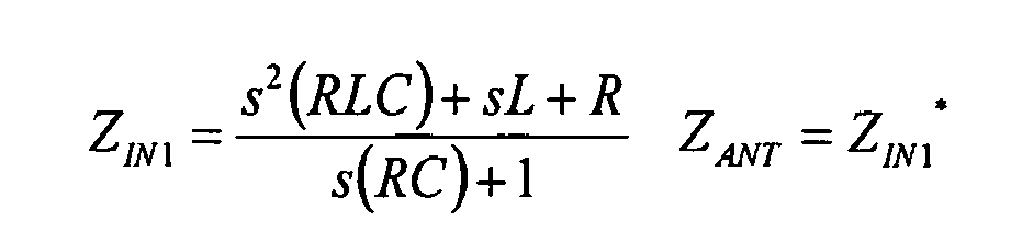
- At Diagram 92, the input impedance is determined at the input of the
tunable coupler 13 as it varies over frequency for the signal, which resolves to:
At Diagram 93, the node equations are then provided at the first and secondtunable capacitors 
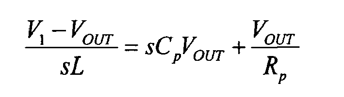
- The transfer function from the
tunable coupler 13 input to the parallel resistance component of the load is provided by the following formula, which is inverted and normalized to unity to provide the aforementioned inverse transfer function.
- As will be appreciated by those skilled in the art, several simulations and measurements of operation of the
RF communications device 10 are now discussed with reference toFIGS. 3-7 . In the measurements, the transmitted signal is modulated using 16-QAM, which is exemplary. - In diagram 30, an actual
transfer function curve 32 and a calculated transfer function curve 31 (using the above formula) for an exemplarytunable coupler 13 are shown. In these measurements, theantenna 14 comprises a 3m whip antenna tuned to 2 MHz using the antenna coupler. At 2 MHz, the input impedance (ZANT) is equal to 10-j1700. Advantageously, the above formula provides a close match to the actualtunable coupler 13 transfer function. Diagram 40 shows anothercurve 41 of the actual transfer function of thetunable coupler 13 along with the filtered base band signal 42 (equalized waveform). - Diagrams 50 and 51 respectively illustrate constellation diagrams for the transmitted 16-QAM signal in the RF communications device without the effects of the coupler equalizer and in the
RF communications device 10. As shown, the distortion introduced by the typical communications device renders the signal unusable whereas theRF communications device 10 increases the SNR of the 16-QAM constellation by approximately 6.7 dB. Diagrams 60 and 61 illustrate eye diagrams for the transmitted signal in a typical communications device and in theRF communications device 10, each again using a 16-QAM modulated signal. - Lastly, diagram 70 shows SNR measurements for the transmitted signal in a
typical communications device 72 operating with a 3 meter whip at 2 MHz and in the RF communications device 10 (72). As is readily shown, the SNR for the transmittedsignal 72 in theRF communications device 10 is significantly greater (17.54 dB) at high data rates. - Advantageously, the
RF communications device 10 compensates for distortion introduced into a transmitted signal by thetunable coupler 13 using an indirect calculation of the tunable coupler's transfer function. More so, the SNR gain for the transmitted signal is achieved with no additional hardware requirements and minor computations costs levied against theprocessor 13. Indeed, the present disclosure provides particular advantages over typical adaptive methods, which typically consume significant processing resources and can be undesirable in mobile applications, for example.
Claims (10)
- A radio frequency (RF) communications device comprising:a power amplifier;an antenna;a tunable coupler between said power amplifier and said antenna;a processor; andan exciter module coupled between said processor and said power amplifier and configured to generate an RF signal based upon a baseband signal;said processor configured to
set said tunable coupler to a desired tuning and thereby defining a transfer function for said tunable coupler,
generate an inverse transfer function of the transfer function of said tunable coupler, and
perform digital filtering upstream of said power amplifier based upon the inverse transfer function. - The RF communications device of Claim 1 wherein said processor is configured to set said tunable coupler by at least selectively matching impedances of said power amplifier and said antenna.
- The RF communications device of Claim 2 wherein said processor is configured to generate the inverse transfer function based upon feedback data from the selective matching of impedances by said tunable coupler.
- The RF communications device of Claim 3 wherein said tunable coupler comprises at least one tunable capacitor, and at least one tunable inductor coupled thereto.
- The RF communications device of Claim 4 wherein said processor is configured to receive the feedback data comprising tunable capacitor and tunable inductor values of said tunable coupler.
- The RF communications device of Claim 1 wherein said processor, said power amplifier, and said tunable coupler are configured to be operable on a 16-Quadrature Amplitude Modulation (QAM) signal.
- A method of operating a radio frequency (RF) communications device comprising a power amplifier, an antenna, a tunable coupler between the power amplifier and the antenna, and an exciter module coupled to the power amplifier, the method comprising:setting the tunable coupler to a desired tuning for defining a transfer function for the tunable coupler;generating an inverse transfer function of the transfer function of the tunable coupler; andperforming digital filtering upstream of the power amplifier based upon the inverse transfer function.
- The method of Claim 7 further comprising setting the tunable coupler by at least selectively matching impedances of the power amplifier and the antenna.
- The method of Claim 8 further comprising generating the inverse transfer function based upon feedback data from the selective matching of impedances by the tunable coupler.
- The method of Claim 9 further comprising using a processor to receive the feedback data comprising tunable capacitor and tunable inductor values of the tunable coupler.
Applications Claiming Priority (1)
| Application Number | Priority Date | Filing Date | Title |
|---|---|---|---|
| US13/170,617 US8433261B2 (en) | 2011-06-28 | 2011-06-28 | RF communications device with inverse function for coupler therein and related methods |
Publications (3)
| Publication Number | Publication Date |
|---|---|
| EP2541780A2 true EP2541780A2 (en) | 2013-01-02 |
| EP2541780A3 EP2541780A3 (en) | 2014-08-06 |
| EP2541780B1 EP2541780B1 (en) | 2016-08-10 |
Family
ID=46704426
Family Applications (1)
| Application Number | Title | Priority Date | Filing Date |
|---|---|---|---|
| EP12004560.4A Active EP2541780B1 (en) | 2011-06-28 | 2012-06-18 | RF communications device with inverse function for coupler therein and related methods |
Country Status (3)
| Country | Link |
|---|---|
| US (1) | US8433261B2 (en) |
| EP (1) | EP2541780B1 (en) |
| IL (1) | IL220312A0 (en) |
Citations (3)
| Publication number | Priority date | Publication date | Assignee | Title |
|---|---|---|---|---|
| US5164959A (en) | 1991-01-22 | 1992-11-17 | Hughes Aircraft Company | Digital equalization method and apparatus |
| US5206600A (en) | 1991-10-18 | 1993-04-27 | Harris Corporation | Impedance determining apparatus using quadrature current and peak detectors |
| US5386194A (en) | 1991-10-18 | 1995-01-31 | Harris Corporation | Digital impedance determination using peak detection of current and voltage samplers |
Family Cites Families (13)
| Publication number | Priority date | Publication date | Assignee | Title |
|---|---|---|---|---|
| US3906405A (en) * | 1974-07-01 | 1975-09-16 | Motorola Inc | Tunable antenna coupling circuit |
| US5923712A (en) * | 1997-05-05 | 1999-07-13 | Glenayre Electronics, Inc. | Method and apparatus for linear transmission by direct inverse modeling |
| US5867065A (en) * | 1997-05-07 | 1999-02-02 | Glenayre Electronics, Inc. | Frequency selective predistortion in a linear transmitter |
| US6400822B1 (en) * | 1997-10-27 | 2002-06-04 | Texas Instruments Incorporated | Linear, optical coupled line impedance circuit |
| US6151354A (en) | 1997-12-19 | 2000-11-21 | Rockwell Science Center | Multi-mode, multi-band, multi-user radio system architecture |
| KR100408043B1 (en) | 2001-09-21 | 2003-12-01 | 엘지전자 주식회사 | Predistortion type digital linearier with digital if circuit |
| US6853246B2 (en) * | 2002-04-18 | 2005-02-08 | Agere Systems Inc. | Adaptive predistortion system and a method of adaptively predistorting a signal |
| US7023929B2 (en) * | 2002-07-10 | 2006-04-04 | Texas Instruments Incorporated | Digital pre-compensation filter for DMT type transmitter |
| US7099399B2 (en) * | 2004-01-27 | 2006-08-29 | Crestcom, Inc. | Distortion-managed digital RF communications transmitter and method therefor |
| US7983327B2 (en) * | 2006-08-28 | 2011-07-19 | Samsung Electronics Co., Ltd. | Method and system for providing digital adaptive predistortion in a subscriber station |
| US7822389B2 (en) | 2006-11-09 | 2010-10-26 | Texas Instruments Incorporated | Methods and apparatus to provide an auxiliary receive path to support transmitter functions |
| US8351874B2 (en) * | 2008-04-08 | 2013-01-08 | Telefonaktiebolaget Lm Ericsson (Publ) | System and method for adaptive antenna impedance matching |
| US8131232B2 (en) * | 2009-10-09 | 2012-03-06 | Texas Instruments Incorporated | Method and apparatus for antenna tuning |
-
2011
- 2011-06-28 US US13/170,617 patent/US8433261B2/en active Active
-
2012
- 2012-06-12 IL IL220312A patent/IL220312A0/en active IP Right Grant
- 2012-06-18 EP EP12004560.4A patent/EP2541780B1/en active Active
Patent Citations (3)
| Publication number | Priority date | Publication date | Assignee | Title |
|---|---|---|---|---|
| US5164959A (en) | 1991-01-22 | 1992-11-17 | Hughes Aircraft Company | Digital equalization method and apparatus |
| US5206600A (en) | 1991-10-18 | 1993-04-27 | Harris Corporation | Impedance determining apparatus using quadrature current and peak detectors |
| US5386194A (en) | 1991-10-18 | 1995-01-31 | Harris Corporation | Digital impedance determination using peak detection of current and voltage samplers |
Also Published As
| Publication number | Publication date |
|---|---|
| US8433261B2 (en) | 2013-04-30 |
| IL220312A0 (en) | 2012-10-31 |
| EP2541780B1 (en) | 2016-08-10 |
| EP2541780A3 (en) | 2014-08-06 |
| US20130005281A1 (en) | 2013-01-03 |
Similar Documents
| Publication | Publication Date | Title |
|---|---|---|
| US7633355B2 (en) | Variable matching circuit | |
| CN1049310C (en) | radio receiver | |
| CN101651480B (en) | Active antenna, base station, method for updating amplitude and phase, and signal processing method | |
| KR100837419B1 (en) | Method and apparatus to compensate AM-PM delay mismatch in envelope restoration transmitter | |
| CN107682292B (en) | High-resolution tuning method and system for active load modulated phase in NFC system | |
| JP2012199923A (en) | System and method for tuning antenna of wireless communication device | |
| US20080233911A1 (en) | Method and system for utilizing a power source as an fm antenna for an integrated fm radio | |
| US20080158076A1 (en) | Dynamically adjustable narrow bandwidth antenna for wide band systems | |
| US11641155B2 (en) | Adaptive harmonic cancellation | |
| US20240014838A1 (en) | Signal processing systems and methods | |
| EP2686965B1 (en) | Compensation of a transmitter distortion | |
| US20190326942A1 (en) | Asymmetric adjacent channel leakage ratio (aclr) control | |
| CN111600620B (en) | A cancellation method of an analog cancellation device for eliminating interference | |
| US9246520B2 (en) | Wideband and multi-band frequency up converter | |
| US20130251010A1 (en) | Method and apparatus for compensating for phase shift in a communication device | |
| RU2264032C2 (en) | Transceiver | |
| EP2541780B1 (en) | RF communications device with inverse function for coupler therein and related methods | |
| US20220123975A1 (en) | Quadrature error correction for radio transceivers | |
| EP1923992A1 (en) | Multi-octave differential upconverter | |
| Zhou et al. | A 64-QAM 45-GHz SiGe transceiver for IEEE 802.11 aj | |
| Castellano et al. | An efficient digital background control for hybrid transformer-based receivers | |
| US8620251B2 (en) | Electronic device with adjustable filter and associated methods | |
| Matsumura | An analog self-interference canceller applicable to 5G NR-based in-band full-duplex supporting 100 MHz bandwidth signal | |
| JP2009253898A (en) | Communication device | |
| US20260058607A1 (en) | Digital voltage reconstruction in a power management circuit |
Legal Events
| Date | Code | Title | Description |
|---|---|---|---|
| PUAI | Public reference made under article 153(3) epc to a published international application that has entered the european phase |
Free format text: ORIGINAL CODE: 0009012 |
|
| 17P | Request for examination filed |
Effective date: 20120618 |
|
| AK | Designated contracting states |
Kind code of ref document: A2 Designated state(s): AL AT BE BG CH CY CZ DE DK EE ES FI FR GB GR HR HU IE IS IT LI LT LU LV MC MK MT NL NO PL PT RO RS SE SI SK SM TR |
|
| AX | Request for extension of the european patent |
Extension state: BA ME |
|
| PUAL | Search report despatched |
Free format text: ORIGINAL CODE: 0009013 |
|
| AK | Designated contracting states |
Kind code of ref document: A3 Designated state(s): AL AT BE BG CH CY CZ DE DK EE ES FI FR GB GR HR HU IE IS IT LI LT LU LV MC MK MT NL NO PL PT RO RS SE SI SK SM TR |
|
| AX | Request for extension of the european patent |
Extension state: BA ME |
|
| RIC1 | Information provided on ipc code assigned before grant |
Ipc: H04B 1/04 20060101AFI20140630BHEP |
|
| 17Q | First examination report despatched |
Effective date: 20150430 |
|
| GRAP | Despatch of communication of intention to grant a patent |
Free format text: ORIGINAL CODE: EPIDOSNIGR1 |
|
| INTG | Intention to grant announced |
Effective date: 20160218 |
|
| GRAR | Information related to intention to grant a patent recorded |
Free format text: ORIGINAL CODE: EPIDOSNIGR71 |
|
| GRAS | Grant fee paid |
Free format text: ORIGINAL CODE: EPIDOSNIGR3 |
|
| GRAA | (expected) grant |
Free format text: ORIGINAL CODE: 0009210 |
|
| INTG | Intention to grant announced |
Effective date: 20160630 |
|
| AK | Designated contracting states |
Kind code of ref document: B1 Designated state(s): AL AT BE BG CH CY CZ DE DK EE ES FI FR GB GR HR HU IE IS IT LI LT LU LV MC MK MT NL NO PL PT RO RS SE SI SK SM TR |
|
| REG | Reference to a national code |
Ref country code: GB Ref legal event code: FG4D |
|
| REG | Reference to a national code |
Ref country code: CH Ref legal event code: EP Ref country code: AT Ref legal event code: REF Ref document number: 819860 Country of ref document: AT Kind code of ref document: T Effective date: 20160815 |
|
| REG | Reference to a national code |
Ref country code: IE Ref legal event code: FG4D |
|
| REG | Reference to a national code |
Ref country code: DE Ref legal event code: R096 Ref document number: 602012021346 Country of ref document: DE |
|
| REG | Reference to a national code |
Ref country code: LT Ref legal event code: MG4D |
|
| REG | Reference to a national code |
Ref country code: NL Ref legal event code: MP Effective date: 20160810 |
|
| REG | Reference to a national code |
Ref country code: AT Ref legal event code: MK05 Ref document number: 819860 Country of ref document: AT Kind code of ref document: T Effective date: 20160810 |
|
| PG25 | Lapsed in a contracting state [announced via postgrant information from national office to epo] |
Ref country code: LT Free format text: LAPSE BECAUSE OF FAILURE TO SUBMIT A TRANSLATION OF THE DESCRIPTION OR TO PAY THE FEE WITHIN THE PRESCRIBED TIME-LIMIT Effective date: 20160810 Ref country code: HR Free format text: LAPSE BECAUSE OF FAILURE TO SUBMIT A TRANSLATION OF THE DESCRIPTION OR TO PAY THE FEE WITHIN THE PRESCRIBED TIME-LIMIT Effective date: 20160810 Ref country code: NL Free format text: LAPSE BECAUSE OF FAILURE TO SUBMIT A TRANSLATION OF THE DESCRIPTION OR TO PAY THE FEE WITHIN THE PRESCRIBED TIME-LIMIT Effective date: 20160810 Ref country code: FI Free format text: LAPSE BECAUSE OF FAILURE TO SUBMIT A TRANSLATION OF THE DESCRIPTION OR TO PAY THE FEE WITHIN THE PRESCRIBED TIME-LIMIT Effective date: 20160810 Ref country code: IS Free format text: LAPSE BECAUSE OF FAILURE TO SUBMIT A TRANSLATION OF THE DESCRIPTION OR TO PAY THE FEE WITHIN THE PRESCRIBED TIME-LIMIT Effective date: 20161210 Ref country code: RS Free format text: LAPSE BECAUSE OF FAILURE TO SUBMIT A TRANSLATION OF THE DESCRIPTION OR TO PAY THE FEE WITHIN THE PRESCRIBED TIME-LIMIT Effective date: 20160810 Ref country code: NO Free format text: LAPSE BECAUSE OF FAILURE TO SUBMIT A TRANSLATION OF THE DESCRIPTION OR TO PAY THE FEE WITHIN THE PRESCRIBED TIME-LIMIT Effective date: 20161110 |
|
| PG25 | Lapsed in a contracting state [announced via postgrant information from national office to epo] |
Ref country code: SE Free format text: LAPSE BECAUSE OF FAILURE TO SUBMIT A TRANSLATION OF THE DESCRIPTION OR TO PAY THE FEE WITHIN THE PRESCRIBED TIME-LIMIT Effective date: 20160810 Ref country code: GR Free format text: LAPSE BECAUSE OF FAILURE TO SUBMIT A TRANSLATION OF THE DESCRIPTION OR TO PAY THE FEE WITHIN THE PRESCRIBED TIME-LIMIT Effective date: 20161111 Ref country code: LV Free format text: LAPSE BECAUSE OF FAILURE TO SUBMIT A TRANSLATION OF THE DESCRIPTION OR TO PAY THE FEE WITHIN THE PRESCRIBED TIME-LIMIT Effective date: 20160810 Ref country code: PT Free format text: LAPSE BECAUSE OF FAILURE TO SUBMIT A TRANSLATION OF THE DESCRIPTION OR TO PAY THE FEE WITHIN THE PRESCRIBED TIME-LIMIT Effective date: 20161212 Ref country code: ES Free format text: LAPSE BECAUSE OF FAILURE TO SUBMIT A TRANSLATION OF THE DESCRIPTION OR TO PAY THE FEE WITHIN THE PRESCRIBED TIME-LIMIT Effective date: 20160810 Ref country code: AT Free format text: LAPSE BECAUSE OF FAILURE TO SUBMIT A TRANSLATION OF THE DESCRIPTION OR TO PAY THE FEE WITHIN THE PRESCRIBED TIME-LIMIT Effective date: 20160810 Ref country code: PL Free format text: LAPSE BECAUSE OF FAILURE TO SUBMIT A TRANSLATION OF THE DESCRIPTION OR TO PAY THE FEE WITHIN THE PRESCRIBED TIME-LIMIT Effective date: 20160810 |
|
| PG25 | Lapsed in a contracting state [announced via postgrant information from national office to epo] |
Ref country code: EE Free format text: LAPSE BECAUSE OF FAILURE TO SUBMIT A TRANSLATION OF THE DESCRIPTION OR TO PAY THE FEE WITHIN THE PRESCRIBED TIME-LIMIT Effective date: 20160810 Ref country code: RO Free format text: LAPSE BECAUSE OF FAILURE TO SUBMIT A TRANSLATION OF THE DESCRIPTION OR TO PAY THE FEE WITHIN THE PRESCRIBED TIME-LIMIT Effective date: 20160810 |
|
| REG | Reference to a national code |
Ref country code: DE Ref legal event code: R097 Ref document number: 602012021346 Country of ref document: DE |
|
| PG25 | Lapsed in a contracting state [announced via postgrant information from national office to epo] |
Ref country code: BG Free format text: LAPSE BECAUSE OF FAILURE TO SUBMIT A TRANSLATION OF THE DESCRIPTION OR TO PAY THE FEE WITHIN THE PRESCRIBED TIME-LIMIT Effective date: 20161110 Ref country code: DK Free format text: LAPSE BECAUSE OF FAILURE TO SUBMIT A TRANSLATION OF THE DESCRIPTION OR TO PAY THE FEE WITHIN THE PRESCRIBED TIME-LIMIT Effective date: 20160810 Ref country code: SK Free format text: LAPSE BECAUSE OF FAILURE TO SUBMIT A TRANSLATION OF THE DESCRIPTION OR TO PAY THE FEE WITHIN THE PRESCRIBED TIME-LIMIT Effective date: 20160810 Ref country code: CZ Free format text: LAPSE BECAUSE OF FAILURE TO SUBMIT A TRANSLATION OF THE DESCRIPTION OR TO PAY THE FEE WITHIN THE PRESCRIBED TIME-LIMIT Effective date: 20160810 Ref country code: SM Free format text: LAPSE BECAUSE OF FAILURE TO SUBMIT A TRANSLATION OF THE DESCRIPTION OR TO PAY THE FEE WITHIN THE PRESCRIBED TIME-LIMIT Effective date: 20160810 Ref country code: BE Free format text: LAPSE BECAUSE OF FAILURE TO SUBMIT A TRANSLATION OF THE DESCRIPTION OR TO PAY THE FEE WITHIN THE PRESCRIBED TIME-LIMIT Effective date: 20160810 |
|
| PLBE | No opposition filed within time limit |
Free format text: ORIGINAL CODE: 0009261 |
|
| STAA | Information on the status of an ep patent application or granted ep patent |
Free format text: STATUS: NO OPPOSITION FILED WITHIN TIME LIMIT |
|
| REG | Reference to a national code |
Ref country code: FR Ref legal event code: PLFP Year of fee payment: 6 |
|
| 26N | No opposition filed |
Effective date: 20170511 |
|
| PG25 | Lapsed in a contracting state [announced via postgrant information from national office to epo] |
Ref country code: SI Free format text: LAPSE BECAUSE OF FAILURE TO SUBMIT A TRANSLATION OF THE DESCRIPTION OR TO PAY THE FEE WITHIN THE PRESCRIBED TIME-LIMIT Effective date: 20160810 |
|
| PG25 | Lapsed in a contracting state [announced via postgrant information from national office to epo] |
Ref country code: MC Free format text: LAPSE BECAUSE OF FAILURE TO SUBMIT A TRANSLATION OF THE DESCRIPTION OR TO PAY THE FEE WITHIN THE PRESCRIBED TIME-LIMIT Effective date: 20160810 |
|
| REG | Reference to a national code |
Ref country code: CH Ref legal event code: PL |
|
| REG | Reference to a national code |
Ref country code: IE Ref legal event code: MM4A |
|
| PG25 | Lapsed in a contracting state [announced via postgrant information from national office to epo] |
Ref country code: CH Free format text: LAPSE BECAUSE OF NON-PAYMENT OF DUE FEES Effective date: 20170630 Ref country code: IE Free format text: LAPSE BECAUSE OF NON-PAYMENT OF DUE FEES Effective date: 20170618 Ref country code: LU Free format text: LAPSE BECAUSE OF NON-PAYMENT OF DUE FEES Effective date: 20170618 Ref country code: LI Free format text: LAPSE BECAUSE OF NON-PAYMENT OF DUE FEES Effective date: 20170630 |
|
| REG | Reference to a national code |
Ref country code: FR Ref legal event code: PLFP Year of fee payment: 7 |
|
| PG25 | Lapsed in a contracting state [announced via postgrant information from national office to epo] |
Ref country code: MT Free format text: LAPSE BECAUSE OF NON-PAYMENT OF DUE FEES Effective date: 20170618 |
|
| PG25 | Lapsed in a contracting state [announced via postgrant information from national office to epo] |
Ref country code: AL Free format text: LAPSE BECAUSE OF FAILURE TO SUBMIT A TRANSLATION OF THE DESCRIPTION OR TO PAY THE FEE WITHIN THE PRESCRIBED TIME-LIMIT Effective date: 20160810 |
|
| REG | Reference to a national code |
Ref country code: DE Ref legal event code: R082 Ref document number: 602012021346 Country of ref document: DE Representative=s name: WUESTHOFF & WUESTHOFF, PATENTANWAELTE PARTG MB, DE Ref country code: DE Ref legal event code: R081 Ref document number: 602012021346 Country of ref document: DE Owner name: HARRIS GLOBAL COMMUNICATIONS, INC., ALBANY, US Free format text: FORMER OWNER: HARRIS CORPORATION, MELBOURNE, FLA., US Ref country code: DE Ref legal event code: R081 Ref document number: 602012021346 Country of ref document: DE Owner name: HARRIS GLOBAL COMMUNICATIONS, INC., ALBANY, US Free format text: FORMER OWNER: HARRIS CORPORATION, MELBOURNE, FL, US |
|
| REG | Reference to a national code |
Ref country code: GB Ref legal event code: 732E Free format text: REGISTERED BETWEEN 20190207 AND 20190213 |
|
| PG25 | Lapsed in a contracting state [announced via postgrant information from national office to epo] |
Ref country code: HU Free format text: LAPSE BECAUSE OF FAILURE TO SUBMIT A TRANSLATION OF THE DESCRIPTION OR TO PAY THE FEE WITHIN THE PRESCRIBED TIME-LIMIT; INVALID AB INITIO Effective date: 20120618 |
|
| PG25 | Lapsed in a contracting state [announced via postgrant information from national office to epo] |
Ref country code: CY Free format text: LAPSE BECAUSE OF NON-PAYMENT OF DUE FEES Effective date: 20160810 |
|
| PG25 | Lapsed in a contracting state [announced via postgrant information from national office to epo] |
Ref country code: MK Free format text: LAPSE BECAUSE OF FAILURE TO SUBMIT A TRANSLATION OF THE DESCRIPTION OR TO PAY THE FEE WITHIN THE PRESCRIBED TIME-LIMIT Effective date: 20160810 |
|
| PG25 | Lapsed in a contracting state [announced via postgrant information from national office to epo] |
Ref country code: TR Free format text: LAPSE BECAUSE OF FAILURE TO SUBMIT A TRANSLATION OF THE DESCRIPTION OR TO PAY THE FEE WITHIN THE PRESCRIBED TIME-LIMIT Effective date: 20160810 |
|
| P01 | Opt-out of the competence of the unified patent court (upc) registered |
Effective date: 20230530 |
|
| PGFP | Annual fee paid to national office [announced via postgrant information from national office to epo] |
Ref country code: DE Payment date: 20250627 Year of fee payment: 14 |
|
| PGFP | Annual fee paid to national office [announced via postgrant information from national office to epo] |
Ref country code: GB Payment date: 20250627 Year of fee payment: 14 |
|
| PGFP | Annual fee paid to national office [announced via postgrant information from national office to epo] |
Ref country code: FR Payment date: 20250625 Year of fee payment: 14 |
|
| PGFP | Annual fee paid to national office [announced via postgrant information from national office to epo] |
Ref country code: IT Payment date: 20250619 Year of fee payment: 14 |