EP2541606A2 - Field transistor structure manufactured using gate last process - Google Patents
Field transistor structure manufactured using gate last process Download PDFInfo
- Publication number
- EP2541606A2 EP2541606A2 EP12004824A EP12004824A EP2541606A2 EP 2541606 A2 EP2541606 A2 EP 2541606A2 EP 12004824 A EP12004824 A EP 12004824A EP 12004824 A EP12004824 A EP 12004824A EP 2541606 A2 EP2541606 A2 EP 2541606A2
- Authority
- EP
- European Patent Office
- Prior art keywords
- layer
- metal
- transistor structure
- field transistor
- polysilicon layer
- Prior art date
- Legal status (The legal status is an assumption and is not a legal conclusion. Google has not performed a legal analysis and makes no representation as to the accuracy of the status listed.)
- Granted
Links
Images




Classifications
-
- H—ELECTRICITY
- H10—SEMICONDUCTOR DEVICES; ELECTRIC SOLID-STATE DEVICES NOT OTHERWISE PROVIDED FOR
- H10D—INORGANIC ELECTRIC SEMICONDUCTOR DEVICES
- H10D64/00—Electrodes of devices having potential barriers
- H10D64/60—Electrodes characterised by their materials
- H10D64/64—Electrodes comprising a Schottky barrier to a semiconductor
- H10D64/647—Schottky drain or source electrodes for IGFETs
-
- G—PHYSICS
- G11—INFORMATION STORAGE
- G11C—STATIC STORES
- G11C17/00—Read-only memories programmable only once; Semi-permanent stores, e.g. manually-replaceable information cards
- G11C17/14—Read-only memories programmable only once; Semi-permanent stores, e.g. manually-replaceable information cards in which contents are determined by selectively establishing, breaking or modifying connecting links by permanently altering the state of coupling elements, e.g. PROM
- G11C17/16—Read-only memories programmable only once; Semi-permanent stores, e.g. manually-replaceable information cards in which contents are determined by selectively establishing, breaking or modifying connecting links by permanently altering the state of coupling elements, e.g. PROM using electrically-fusible links
Definitions
- the invention relates to a field transistor gate structure produced according to various foundry production techniques as well as novel processes for producing the field transistor gate structure.
- a field transistor structure includes a semiconductor substrate, a metal gate, a polycrystalline silicon (polysilicon) layer, and first and second metal portions.
- the polysilicon layer has first, second, third, and fourth sides and is disposed between the semiconductor substrate on the first side and the metal gate on the second side.
- the polysilicon layer is also disposed between the first and second metal portions on the third and fourth sides.
- the field transistor structure may also include a thin metal layer (or a combination of multiple different metal layers) disposed between the polysilicon layer and the semiconductor substrate.
- the thin metal layer may be electronically coupled to each of the first and second metal portions.
- An inter-layer dielectric (ILD) may also be disposed between the metal gate and the polysilicon layer.
- a one-time programmable device may include a semiconductor substrate and a plurality of programmable elements formed on the semiconductor substrate.
- the programmable elements can each include a metal gate, first and second metal portions, and a polysilicon layer.
- the polysilicon layer has first, second, third, and fourth sides and is disposed between the semiconductor substrate on the first side and the metal gate on the second side. Additionally, the polysilicon layer is disposed between the first and second metal portions on the third and fourth sides.
- a thin metal layer or a combination of multiple different metal layers may be disposed between the polysilicon layer and the semiconductor substrate. Additionally, the thin metal layer may be electrically coupled to the first and second metal portions.
- the programmable elements may also include an ILD disposed between the metal gate and the polysilicon layer.
- a method of making a field transistor structure includes depositing a first dielectric layer on a silicon substrate.
- a thin metal layer (or a combination of multiple different metal layers) is deposited on top of the first dielectric layer and a polysilicon layer is deposited on top of the thin metal layer.
- First and second portions are then removed from the polysilicon layer and backfilled with first and second metal portions.
- a metal gate is deposited on top of the field transistor structure.
- the method may also include depositing a second dielectric layer between the polysilicon layer and the metal gate according to embodiments of the invention.
- the substrate may constitute silicon or silicon with a shallow trench isolation (STI) layer on top.
- STI shallow trench isolation
- a field transistor structure comprises:
- the field transistor structure further comprises a thin metal layer disposed between said polysilicon layer and said semiconductor substrate, wherein said thin metal layer electrically couples said first and second metal portions to each other.
- said thin metal layer is configured to increase its resistance in response to a high current being applied between said first and second metal portions.
- the field transistor structure further comprises an inter-layer dielectric (ILD) disposed between said metal gate and said polysilicon layer.
- ILD inter-layer dielectric
- the conductance of said polysilicon layer between said first and second metal portions varies with a voltage applied to said metal gate.
- the conductance of said polysilicon layer between said first and second metal portions varies with the frequency of a signal applied between said first and second metal portions.
- the layer comprises Ti, TiN, TaN, AL, Ta, Mo, or W.
- said polysilicon layer is lightly doped.
- said polysilicon layer is an intrinsic semiconductor.
- the field transistor structure further comprises a dielectric layer disposed between said metal layer and said semiconductor substrate.
- said dielectric layer is a hi-k material, oxide, nitride, or oxinitride, or their combination.
- the field transistor structure further comprises a shallow trench isolation (STI) layer disposed between said dielectric layer and said semiconductor substrate.
- STI shallow trench isolation
- a conductive channel is formed in the polysilicon layer when a gate voltage is applied to said metal gate, thereby forming a field effect transistor having the first and second metal portions operate as a respective source and drain of the field effect transistor.
- the thin metal layer changes impedance with the application of the high current to the first and second metal portions, thereby forming a one-time programmable (OTP) memory.
- OTP one-time programmable
- a method is provided of making a field transistor structure, comprising:
- the method further comprises depositing a second dielectric layer between said polysilicon layer and said metal gate.
- the method further comprises forming first and second contacts to said first and second metal portions through said second dielectric layer.
- the method further comprises defining a spacer portion on said silicon substrate by a combination of deposition, lithography, etching, and chemical mechanical polishing (CMP).
- CMP chemical mechanical polishing
- said silicon substrate has one or more oxide or shallow-trench isolation (STI) layers on top of it.
- STI shallow-trench isolation
- one or more of said metal layer, first metal portion, second metal portion, and metal gate is made from Ti, TiN, TaN, AL, Ta, Mo, or W.
- said dielectric layer comprises a hi-k material, oxide, nitride, oxinitride, or any combination thereof.
- said polysilicon layer is undoped.
- said polysilicon layer is lightly doped.
- said depositing steps comprise PVD, CVD, or ALD processes.
- FIG. 1a depicts a partially-completed field transistor structure according to embodiments of the present invention.
- FIG. 1b depicts a partially-completed field transistor structure according to embodiments of the present invention.
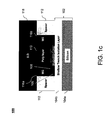
- FIG. 1c depicts a partially-completed field transistor structure according to embodiments of the present invention.
- FIG. 1d depicts a field transistor structure according to embodiments of the present invention.
- FIG. 2 is a flow chart depicting a process for making a field transistor structure according to embodiments of the present invention.
- FIG. 3 is a depiction of the conventional circuit components used to model the field transistor structure according to embodiments of the present invention.
- FIG. 4 is a flow chart depicting a method of using the field transistor structure according to embodiments of the present invention.
- FIG. 5 is a graph depicting the resistance of the polysilicon as a function of the voltage applied to the gate metal according to embodiments of the present invention.
- FIG. 6 is a graph depicting the resistance of the polysilicon as a function of the frequency of a signal applied between a source and a drain of a transistor structure according to embodiments of the present invention.
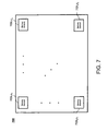
- FIG. 7 is a functional block diagram of a one-time programmable memory according to embodiments of the present invention.
- a flexible field transistor structure is described herein, in addition to the process for making the same.
- the flexible transistor structure can provide multiple circuit functions from a single transistor structure, including: low performance field effect transistor (FET), fuse or one time programmable memory, and high resistance resistor having a frequency dependent resistance or conductance.
- FET field effect transistor
- the process for making the multi-functional transistor structure is implemented by modifying the gate region processing that is available in conventional foundry processes, for example a 28nm process that uses a high-K dielectric for gate formation.
- FIGs. 1a-d depict process flow for creating a field transistor gate structure according to embodiments of the present invention.
- FIG. 1a depicts a field transistor structure 100 according to embodiments of the present invention.
- the transistor structure 100 is built on a silicon substrate 102.
- the silicon substrate may include a silicon layer 104a and a shallow-trench isolation (STI) layer 104b deposited on top of it.
- the silicon substrate 102 may include the silicon layer 104a without the STI layer 104b.
- Dielectric layer 106 is disposed on the silicon substrate 102.
- the dielectric layer 106 may comprise a high-k dielectric in order to increase gate capacitance and, therefore, improve the performance of regular transistors located on the same wafer as field transistor structure 100.
- dielectric layer comprises a hi-k dielectric material, oxide, nitride, oxinitride, or any other suitable dielectric material. Additionally, the dielectric layer may include several suitable dielectric materials in combination with one another.
- a thin metal layer 108 is deposited on top of the dielectric layer 106.
- the thickness of the thin metal layer 108 can be adjusted to achieve desired a resistivity; when a lower resistivity is desired, the thickness of the thin metal layer 108 can be increased, and vice versa for a higher resistivity.
- the thin metal layer 108 can comprise titanium, titanium nitride, tantalum, tantalum nitride, aluminum, tungsten, or any other suitable metal or metal alloy. Additionally, the thin metal layer can comprise any combination of suitable metals or metal alloys.
- the thin metal layer can be deposited by physical vapor deposition (PVD), chemical vapor deposition (CVD), atomic layer deposition (ALD), or any other suitable method of deposition.
- a polysilicon layer 110 is deposited on top of metal layer 108 according to well-known processes.
- the polysilicon layer is entirely un-doped or very lightly doped (i.e., on the order of 10 13 atoms/cm 3 ).
- Spacers 112 are also deposited and can be defined by a combination of deposition, lithography, etching, and chemical-mechanical planarization. The spacers 112 are used to electrically isolate the transistor structure 100 from surrounding structures. The spacers 112 are preferably made out of a dielectric material for that purpose.
- FIG. 1b depicts the field transistor structure 100 after a portion of the poly layer 110 has been etched away to form recesses 114a and 114b. While FIG. 1b depicts recesses 114a and 114b extending to the top of metal layer 108, according to some embodiments of the invention, a corresponding portion of the metal layer 108 could also be etched away causing recesses 114a and 114b to extend to the top of dielectric layer 106.
- the recesses 114a and 114b can then be back filled with metal to form metal portions 116a and 116b.
- the recesses 114a and 114b can be back filled using PVD, CVD, ALD, or any other suitable method of deposition.
- the metal portions 116a and 116b can comprise titanium, titanium nitride, tantalum, tantalum nitride, aluminum, tungsten, or any other suitable metal or metal alloy. Additionally, the metal portions 116a and 116b can also comprise any combination of suitable metals or metal alloys. Chemical mechanical polish (CMP) may be needed to planarize the surface and leave the metal in the trench.
- CMP Chemical mechanical polish
- An inter-layer dielectric (ILD) layer can be formed on top of the polysilicon layer 110, spacers 112, and metal portions 116a and 116b.
- the ILD is on the order of 70-80 nanometers thick, however, other thickness may be used depending on the particular process and application.
- FIG. 1d depicts a completed field transistor structure 100 according to embodiments of the present invention.
- the completed field transistor structure 100 includes contacts 120a and 120b, which are formed through the ILD 118. Each of the contacts 120a and 120b corresponds to a metal portion 116a and 116b and is electrically coupled to it.
- the completed field transistor structure 100 also includes a metal gate portion 122 formed on top of the ILD layer 118.
- the polysilicon layer 110 includes first, second, third, and fourth sides, where: the polysilicon layer is disposed between the semiconductor substrate on the first side and the metal gate on said second side; and where the polysilicon layer 110 is disposed between the first and second metal portions 116a and 116b on the third and fourth sides.
- the bottom surface (or first side) of the polysilicon layer 110 is in direct contact with the top surface of the metal layer 108; the top surface (or second side) of the polysilicon layer 110 is in direct contact with the bottom surface of the ILD layer 110; the first side surface (third side) of the polysilicon layer 110 is in direct contact with the first metal portion 116a; and the second side surface (fourth side) of the polysilicon layer 110 is in direct contact with the second metal portion 116b.
- FIG. 2 is a flowchart depicting a process 200 for making the field transistor structure 100 according to embodiments of the present invention. This process will be described with reference to FIGS 1a-d and FIG. 2 .
- a dielectric layer 106 is deposited on a silicon substrate 102 at step 202.
- the silicon substrate 102 may comprise a silicon layer 104a or a silicon layer 104a and an STI layer 104b.
- a metal layer 108 is deposited on top of the dielectric layer 106.
- the metal layer 108 may be deposited by using PVD, CVD, ALD, or any other appropriate process for metal deposition.
- the metal layer 108 may also include any appropriate metal such as titanium, titanium nitride, tantalum, tantalum nitride, aluminum, tungsten, or any other suitable metal or metal alloy.
- the metal layer 108 may also comprise a combination of suitable metals or alloys.
- a polysilicon layer 110 is deposited on top of the metal layer 108.
- the polysilicon layer 110 is preferably un-doped or very lightly doped (i.e., on the order of 10 13 atoms/cm 3 ).
- the transistor structure 100 can be patterned using lithography and etching. Spacers 112 can be defined by a combination of deposition, lithography, etching, and CMP (chemical mechanical polishing) at step 210, and a portion of the polysilicon layer 110 can then be removed to form recesses 114a and 114b at step 212. Additionally, a portion of the metal layer 108 corresponding to the portion of the polysilicon layer 110 that was removed can also be removed according to embodiments of the present invention.
- the recesses 114a and 114b can be backfilled with metal to form first and second metal portions 116a and 116b at step 214.
- An ILD 118 may then be deposited and contacts 120a and 120b formed through the ILD and electrically coupled to the first and second metal portions 116a and 116b, respectively at step 216.
- a metal gate 122 may be deposited on ILD 118 and patterned at step 218 to complete the formation of the field transistor structure.
- FIG. 3 illustrates a circuit model 300 of the field transistor structure according to embodiments of the present invention.
- the interface between the metal portions and the poly layer can be modeled using Schottky diodes D1 and D2.
- the resistance of the poly layer is modeled by resistor R5.
- the value of R5 is a function of the metal gate voltage and the frequency of the signal between the source and the drain.
- Capacitors C1 and C2 are used to model the parasitic capacitance between the metal portions and the substrate.
- Capacitor C3 is used to model the parasitic capacitance between the metal layer and the substrate.
- Resistors R1 and R2 model the resistance between the contacts and the MG layers.
- R3 and R4 model the resistance between the metal portions and the metal layer.
- R6 models the resistance of the thin metal layer. According to embodiments of the present invention, R6 is large due to the thinness of the thin metal layer. R5, however, can be much larger than R6 as much as 2 or 3 orders of magnitude, according to some
- FIG. 4 illustrates a method 400 of using the field transistor structure 100 according to embodiments of the present invention.
- a voltage is applied to the metal gate portion 122.
- a signal is applied between the first and second metal portions 116a and 116b at step 404.
- the voltage level applied to the metal gate 122 can be varied to modify the resistance of the poly layer 110 at step 406.
- the frequency of the signal applied between the first and second metal portions 116a and 116b can be varied to change the resistance of the poly layer 110 at step 406.
- the un-doped or lightly doped polysilicon layer 110 of the present invention exhibits very high electrical resistance.
- voltage applied to metal gate 122 induces a charge in the polysilicon layer 110 by both inversion and accumulation, to create a channel for conduction. This modulates the resistance of the polysilicon layer 110 so that the structure can be used as a field effect transistor (FET) when voltage is applied to the gate, described further below.
- FET field effect transistor
- Thin metal layer 108 has a very high resistance because it is so thin, and therefore does not impede the transistor features once the channel is created even though the thin metal layer 108 provides a parallel electrical path between the source and drain.
- the resistance of the polysilicon layer begins at a high value 502 when no voltage is applied to the gate. However, as the applied voltage increases, the resistance decreases. For instance, according to some applications, the resistance value can change several percentage points when the gate voltage falls below 3V.
- the resistance of the polysilicon also varies with the frequency of a voltage signal applied between the source 116a and the drain 116b.
- the un-doped or lightly doped polysilicon layer 110 exhibits high resistance when a relatively low frequency voltage signal is applied between the source 116a and drain 116b, and a lower resistance when a higher frequency voltage signal is applied between the source 116a and drain 116b. Maintaining a constant frequency signal, will maintain a relatively constant resistivity, all other factors remaining the same. Further the variation in resistance of the polysilicon with frequency can be overcome or compensated by adjusting the gate voltage.
- the conductivity of the polysilicon 110 can be maintained by increasing the voltage on metal gate 122, assuming there is headroom to do so.
- the conductivity of the polysilicon 110 can be maintained by decreasing the voltage on metal gate 122, assuming there is headroom to do so.
- FIG. 6 This relationship between the resistance of the polysilicon layer 110 and the frequency of the voltage signal applied between the source 116a and the drain 116b is graphically shown in FIG. 6 .
- the polysilicon layer 110 exhibits a high resistance 602 when the frequency of the applied voltage signal is low (e.g., a DC voltage).
- the resistance can change by several percentage points when the frequency increases to the RF spectrum compared to lower frequencies.
- Completed field transistor structure 100 is operable as a field effect transistor (FET), as described above.
- FET field effect transistor
- the metal portions 116a and 116b are operable as the source and drain, respectively, and connected through metal contacts 120a and 120b.
- the metal gate portion 122 can operate as a transistor gate, so that a voltage applied to the gate 122 creates a channel in the polysilicon layer for current flow.
- the transistor structure 100 is capable of operating as a FET due to the characteristic of the un-doped/lightly doped polysilicon layer 110.
- the formed channel is not as low resistance as would be with a thin gate dielectric, but it is functional for circuit applications that do not require high FET performance.
- the thin metal layer 108 provides a parallel current path between the source and drain 116.
- the resistance change due to applied gate voltage can be significant compared to the thin metal resistance, and therefore does not degrade the FET performance once a gate voltage is applied and the channel is formed.
- the transistor structure 100 can be used as a component of a one-time programmable (OTP) device.
- FIG. 7 illustrates an OTP device 700 according to embodiments of the present invention.
- the device 700 can include a number of programmable elements 702r 1 c 1 to 702r x c y .
- Each of the device elements comprises a transistor structure 100 such as that depicted in FIG. 1d .
- the individual elements 702 can be programmed by connecting a large voltage across metal portions 116a and 116b, to force a large current through the metal layer 108.
- the metal layer 108 provides an electrical connection between metal portions 116a and 116b, that has a high resistance. Accordingly, applying a high current to the thin metal layer 108 can cause the thin metal layer 108 to behave like a fuse and blow due to heating. That is, the thin metal layer 108, according to some embodiments, entirely severs the electrical connection that it created between metal portions 116a and 116b upon application of high current. According to other embodiments, the electrical connection between 116a and 116b created by the thin metal layer remains, but the resistance of the thin metal layer is greatly increased in response to application of high current.
- the impedance from source-to-drain 116 of the device will significantly change, so that it can be used as a fuse or OTP memory.
- the thin metal layer operates as a fuse that may be blown where a binary zero is to be stored, and remain unaltered where a binary one is to be stored.
- the binary-zero/binary-one representations may be reversed as will be understood by those skilled in the art. (i.e. the blown fuse could represent a binary 1, and the intact option represents a binary 0)
- the memory can be subsequently read by measuring the impedance across the source drain contacts.
- the transistor structure 100 can be used as a high resistance resistor, and more specifically a frequency dependent resistor.
- the polysilicon layer 110 is low doped and has an inherently high resistance when no gate voltage is applied to the metal gate 122. Therefore, the source/drain contacts 120a,b can be used a high resistance resistor in an IC device.
- the resistor is frequency dependent due to the properties of the polysilicon/metal interface described herein, and therefore a frequency dependent resistor can be created simply by adjusting the frequency of the input signal applied to the source/drain contacts 120a,b.
Landscapes
- Insulated Gate Type Field-Effect Transistor (AREA)
- Metal-Oxide And Bipolar Metal-Oxide Semiconductor Integrated Circuits (AREA)
- Electrodes Of Semiconductors (AREA)
Abstract
Description
- The invention relates to a field transistor gate structure produced according to various foundry production techniques as well as novel processes for producing the field transistor gate structure.
- Due to the exorbitant cost of the equipment required for the production of semiconductor components, many semiconductor companies outsource the actual manufacture of their semiconductor components to specialized semiconductor foundries. While a foundry may have many customers that each require a wide variety of different semiconductor components, it will typically require that each of its customers submit designs consisting of components from standard library in order to facilitate use of a common processes for manufacturing the components for all of its customers.
- For some customers the components from the standard library are not sufficient to meet all of their needs. For instance, a customer may wish to use components that are not part of the standard library. However, foundries are often unwilling or unable to alter their process steps on a customer-by-customer basis. Thus, there exists a need for new components manufactured according to existing foundry processes.
- According to embodiments of the invention, a field transistor structure is provided. The field transistor structure includes a semiconductor substrate, a metal gate, a polycrystalline silicon (polysilicon) layer, and first and second metal portions. The polysilicon layer has first, second, third, and fourth sides and is disposed between the semiconductor substrate on the first side and the metal gate on the second side. The polysilicon layer is also disposed between the first and second metal portions on the third and fourth sides. According to some embodiments of the present invention, the field transistor structure may also include a thin metal layer (or a combination of multiple different metal layers) disposed between the polysilicon layer and the semiconductor substrate. The thin metal layer may be electronically coupled to each of the first and second metal portions. An inter-layer dielectric (ILD) may also be disposed between the metal gate and the polysilicon layer.
- According to embodiments of the invention, a one-time programmable device is provided. The one-time programmable device may include a semiconductor substrate and a plurality of programmable elements formed on the semiconductor substrate. The programmable elements can each include a metal gate, first and second metal portions, and a polysilicon layer. The polysilicon layer has first, second, third, and fourth sides and is disposed between the semiconductor substrate on the first side and the metal gate on the second side. Additionally, the polysilicon layer is disposed between the first and second metal portions on the third and fourth sides. A thin metal layer or a combination of multiple different metal layers may be disposed between the polysilicon layer and the semiconductor substrate. Additionally, the thin metal layer may be electrically coupled to the first and second metal portions. The programmable elements may also include an ILD disposed between the metal gate and the polysilicon layer.
- According to embodiments of the invention, a method of making a field transistor structure is provided. The method includes depositing a first dielectric layer on a silicon substrate. A thin metal layer (or a combination of multiple different metal layers) is deposited on top of the first dielectric layer and a polysilicon layer is deposited on top of the thin metal layer. First and second portions are then removed from the polysilicon layer and backfilled with first and second metal portions. A metal gate is deposited on top of the field transistor structure. The method may also include depositing a second dielectric layer between the polysilicon layer and the metal gate according to embodiments of the invention. According to some embodiments the substrate may constitute silicon or silicon with a shallow trench isolation (STI) layer on top.
- Further features and advantages of the invention, as well as the structure and operation of various embodiments of the invention, are described in detail below with reference to the accompanying drawings. It is noted that the invention is not limited to the specific embodiments described herein. Such embodiments are presented herein for illustrative purposes only.
- According to an aspect, a field transistor structure comprises:
- a semiconductor substrate;
- a metal gate;
- first and second metal portions; and
- a polysilicon layer having first, second, third, and fourth sides, wherein said polysilicon layer is disposed between said semiconductor substrate on said first side and said metal gate on said second side; and
- wherein said polysilicon layer is disposed between said first and second metal portions on said third and fourth sides.
- Advantageously, the field transistor structure further comprises a thin metal layer disposed between said polysilicon layer and said semiconductor substrate, wherein said thin metal layer electrically couples said first and second metal portions to each other.
- Advantageously, said thin metal layer is configured to increase its resistance in response to a high current being applied between said first and second metal portions.
- Advantageously, the field transistor structure further comprises an inter-layer dielectric (ILD) disposed between said metal gate and said polysilicon layer.
- Advantageously, the conductance of said polysilicon layer between said first and second metal portions varies with a voltage applied to said metal gate.
- Advantageously, the conductance of said polysilicon layer between said first and second metal portions varies with the frequency of a signal applied between said first and second metal portions.
- Advantageously, the layer comprises Ti, TiN, TaN, AL, Ta, Mo, or W.
- Advantageously, said polysilicon layer is lightly doped.
- Advantageously, said polysilicon layer is an intrinsic semiconductor.
- Advantageously, the field transistor structure further comprises a dielectric layer disposed between said metal layer and said semiconductor substrate.
- Advantageously, said dielectric layer is a hi-k material, oxide, nitride, or oxinitride, or their combination.
- Advantageously, the field transistor structure further comprises a shallow trench isolation (STI) layer disposed between said dielectric layer and said semiconductor substrate.
- Advantageously, a conductive channel is formed in the polysilicon layer when a gate voltage is applied to said metal gate, thereby forming a field effect transistor having the first and second metal portions operate as a respective source and drain of the field effect transistor.
- Advantageously, the thin metal layer changes impedance with the application of the high current to the first and second metal portions, thereby forming a one-time programmable (OTP) memory.
- According to an aspect, a method is provided of making a field transistor structure, comprising:
- depositing a first dielectric layer on a silicon substrate;
- depositing a thin metal layer on top of said silicon substrate;
- depositing a polysilicon layer on top of said thin metal layer;
- removing first and second portions from said polysilicon layer and backfilling the removed portions with first and second metal portions; and
- depositing a metal gate on top of said field transistor structure.
- Advantageously, the method further comprises depositing a second dielectric layer between said polysilicon layer and said metal gate.
- Advantageously, the method further comprises forming first and second contacts to said first and second metal portions through said second dielectric layer.
- Advantageously, the method further comprises defining a spacer portion on said silicon substrate by a combination of deposition, lithography, etching, and chemical mechanical polishing (CMP).
- Advantageously, said silicon substrate has one or more oxide or shallow-trench isolation (STI) layers on top of it.
- Advantageously, one or more of said metal layer, first metal portion, second metal portion, and metal gate is made from Ti, TiN, TaN, AL, Ta, Mo, or W.
- Advantageously, said dielectric layer comprises a hi-k material, oxide, nitride, oxinitride, or any combination thereof.
- Advantageously, said polysilicon layer is undoped.
- Advantageously, said polysilicon layer is lightly doped.
- Advantageously, said depositing steps comprise PVD, CVD, or ALD processes.
- Additional embodiments will be apparent to a person skilled in the relevant art(s) based on the teachings contained herein.
- Embodiments of the invention are described with reference to the accompanying drawings. In the drawings, like reference numbers indicate identical or functionally similar elements. Additionally, the left most digit(s) of a reference number identifies the drawing in which the reference number first appears.
-
FIG. 1a depicts a partially-completed field transistor structure according to embodiments of the present invention. -
FIG. 1b depicts a partially-completed field transistor structure according to embodiments of the present invention. -
FIG. 1c depicts a partially-completed field transistor structure according to embodiments of the present invention. -
FIG. 1d depicts a field transistor structure according to embodiments of the present invention. -
FIG. 2 is a flow chart depicting a process for making a field transistor structure according to embodiments of the present invention. -
FIG. 3 is a depiction of the conventional circuit components used to model the field transistor structure according to embodiments of the present invention. -
FIG. 4 is a flow chart depicting a method of using the field transistor structure according to embodiments of the present invention. -
FIG. 5 is a graph depicting the resistance of the polysilicon as a function of the voltage applied to the gate metal according to embodiments of the present invention. -
FIG. 6 is a graph depicting the resistance of the polysilicon as a function of the frequency of a signal applied between a source and a drain of a transistor structure according to embodiments of the present invention. -
FIG. 7 is a functional block diagram of a one-time programmable memory according to embodiments of the present invention. - The invention will now be described with reference to the accompanying drawings. In the drawings, like reference numbers generally indicate identical, functionally similar, and/or structurally similar elements. The drawing in which an element first appears is indicated by the leftmost digit(s) in the reference number.
- The following Detailed Description refers to accompanying drawings to illustrate exemplary embodiments consistent with the invention. References in the Detailed Description to "one exemplary embodiment," "an exemplary embodiment," "an example exemplary embodiment," etc., indicate that the exemplary embodiment described may include a particular feature, structure, or characteristic, but every exemplary embodiment may not necessarily include the particular feature, structure, or characteristic. Moreover, such phrases are not necessarily referring to the same exemplary embodiment. Further, when a particular feature, structure, or characteristic is described in connection with an exemplary embodiment, it is within the knowledge of those skilled in the relevant art(s) to effect such feature, structure, or characteristic in connection with other exemplary embodiments whether or not explicitly described.
- The exemplary embodiments described herein are provided for illustrative purposes, and are not limiting. Other exemplary embodiments are possible, and modifications may be made to the exemplary embodiments within the spirit and scope of the invention. Therefore, the Detailed Description is not meant to limit the invention. Rather, the scope of the invention is defined only in accordance with the following claims and their equivalents.
- The following Detailed Description of the exemplary embodiments will so fully reveal the general nature of the invention that others can, by applying knowledge of those skilled in relevant art(s), readily modify and/or adapt for various applications such exemplary embodiments, without undue experimentation, without departing from the spirit and scope of the invention. Therefore, such adaptations and modifications are intended to be within the meaning and plurality of equivalents of the exemplary embodiments based upon the teaching and guidance presented herein. It is to be understood that the phraseology or terminology herein is for the purpose of description and not of limitation, such that the terminology or phraseology of the present specification is to be interpreted by those skilled in relevant art(s) in light of the teachings herein.
- A flexible field transistor structure is described herein, in addition to the process for making the same. The flexible transistor structure can provide multiple circuit functions from a single transistor structure, including: low performance field effect transistor (FET), fuse or one time programmable memory, and high resistance resistor having a frequency dependent resistance or conductance. Further, the process for making the multi-functional transistor structure is implemented by modifying the gate region processing that is available in conventional foundry processes, for example a 28nm process that uses a high-K dielectric for gate formation.
-
FIGs. 1a-d depict process flow for creating a field transistor gate structure according to embodiments of the present invention. -
FIG. 1a depicts afield transistor structure 100 according to embodiments of the present invention. Thetransistor structure 100 is built on asilicon substrate 102. According to embodiments of the present invention, the silicon substrate may include asilicon layer 104a and a shallow-trench isolation (STI)layer 104b deposited on top of it. Alternatively, thesilicon substrate 102 may include thesilicon layer 104a without theSTI layer 104b.Dielectric layer 106 is disposed on thesilicon substrate 102. According to some embodiments, thedielectric layer 106 may comprise a high-k dielectric in order to increase gate capacitance and, therefore, improve the performance of regular transistors located on the same wafer asfield transistor structure 100. According to some embodiments, dielectric layer comprises a hi-k dielectric material, oxide, nitride, oxinitride, or any other suitable dielectric material. Additionally, the dielectric layer may include several suitable dielectric materials in combination with one another. - A
thin metal layer 108 is deposited on top of thedielectric layer 106. The thickness of thethin metal layer 108 can be adjusted to achieve desired a resistivity; when a lower resistivity is desired, the thickness of thethin metal layer 108 can be increased, and vice versa for a higher resistivity. According to embodiments of the invention, thethin metal layer 108 can comprise titanium, titanium nitride, tantalum, tantalum nitride, aluminum, tungsten, or any other suitable metal or metal alloy. Additionally, the thin metal layer can comprise any combination of suitable metals or metal alloys. The thin metal layer can be deposited by physical vapor deposition (PVD), chemical vapor deposition (CVD), atomic layer deposition (ALD), or any other suitable method of deposition. Apolysilicon layer 110 is deposited on top ofmetal layer 108 according to well-known processes. Preferably, the polysilicon layer is entirely un-doped or very lightly doped (i.e., on the order of 1013 atoms/cm3).Spacers 112 are also deposited and can be defined by a combination of deposition, lithography, etching, and chemical-mechanical planarization. Thespacers 112 are used to electrically isolate thetransistor structure 100 from surrounding structures. Thespacers 112 are preferably made out of a dielectric material for that purpose. -
FIG. 1b depicts thefield transistor structure 100 after a portion of thepoly layer 110 has been etched away to formrecesses FIG. 1b depictsrecesses metal layer 108, according to some embodiments of the invention, a corresponding portion of themetal layer 108 could also be etched away causingrecesses dielectric layer 106. - As shown in
FIG. 1c , therecesses metal portions recesses metal portions metal portions polysilicon layer 110,spacers 112, andmetal portions -
FIG. 1d depicts a completedfield transistor structure 100 according to embodiments of the present invention. As can be seen, the completedfield transistor structure 100 includescontacts ILD 118. Each of thecontacts metal portion field transistor structure 100 also includes ametal gate portion 122 formed on top of theILD layer 118. Thepolysilicon layer 110 includes first, second, third, and fourth sides, where: the polysilicon layer is disposed between the semiconductor substrate on the first side and the metal gate on said second side; and where thepolysilicon layer 110 is disposed between the first andsecond metal portions polysilicon layer 110 is in direct contact with the top surface of themetal layer 108; the top surface (or second side) of thepolysilicon layer 110 is in direct contact with the bottom surface of theILD layer 110; the first side surface (third side) of thepolysilicon layer 110 is in direct contact with thefirst metal portion 116a; and the second side surface (fourth side) of thepolysilicon layer 110 is in direct contact with thesecond metal portion 116b. -
FIG. 2 is a flowchart depicting aprocess 200 for making thefield transistor structure 100 according to embodiments of the present invention. This process will be described with reference toFIGS 1a-d andFIG. 2 . As shown inFIG. 2 , adielectric layer 106 is deposited on asilicon substrate 102 atstep 202. According to embodiments of the present invention, thesilicon substrate 102 may comprise asilicon layer 104a or asilicon layer 104a and anSTI layer 104b. - At
step 204, ametal layer 108 is deposited on top of thedielectric layer 106. According to embodiments of the present invention, themetal layer 108 may be deposited by using PVD, CVD, ALD, or any other appropriate process for metal deposition. Themetal layer 108 may also include any appropriate metal such as titanium, titanium nitride, tantalum, tantalum nitride, aluminum, tungsten, or any other suitable metal or metal alloy. Themetal layer 108 may also comprise a combination of suitable metals or alloys. - At
step 206, apolysilicon layer 110 is deposited on top of themetal layer 108. Thepolysilicon layer 110 is preferably un-doped or very lightly doped (i.e., on the order of 1013 atoms/cm3). Atstep 208, thetransistor structure 100 can be patterned using lithography and etching.Spacers 112 can be defined by a combination of deposition, lithography, etching, and CMP (chemical mechanical polishing) atstep 210, and a portion of thepolysilicon layer 110 can then be removed to formrecesses step 212. Additionally, a portion of themetal layer 108 corresponding to the portion of thepolysilicon layer 110 that was removed can also be removed according to embodiments of the present invention. - The
recesses second metal portions step 214. AnILD 118 may then be deposited andcontacts second metal portions step 216. Ametal gate 122 may be deposited onILD 118 and patterned atstep 218 to complete the formation of the field transistor structure. -
FIG. 3 illustrates acircuit model 300 of the field transistor structure according to embodiments of the present invention. Because it is non-ohmic, the interface between the metal portions and the poly layer can be modeled using Schottky diodes D1 and D2. The resistance of the poly layer is modeled by resistor R5. The value of R5 is a function of the metal gate voltage and the frequency of the signal between the source and the drain. Capacitors C1 and C2 are used to model the parasitic capacitance between the metal portions and the substrate. Capacitor C3 is used to model the parasitic capacitance between the metal layer and the substrate. Resistors R1 and R2 model the resistance between the contacts and the MG layers. R3 and R4 model the resistance between the metal portions and the metal layer. R6 models the resistance of the thin metal layer. According to embodiments of the present invention, R6 is large due to the thinness of the thin metal layer. R5, however, can be much larger than R6 as much as 2 or 3 orders of magnitude, according to some embodiments. -
FIG. 4 illustrates amethod 400 of using thefield transistor structure 100 according to embodiments of the present invention. As is shown ifFIG. 4 , a voltage is applied to themetal gate portion 122. Next a signal is applied between the first andsecond metal portions step 404. The voltage level applied to themetal gate 122 can be varied to modify the resistance of thepoly layer 110 atstep 406. Finally, the frequency of the signal applied between the first andsecond metal portions poly layer 110 atstep 406. - In general, the un-doped or lightly doped
polysilicon layer 110 of the present invention exhibits very high electrical resistance. However, voltage applied tometal gate 122 induces a charge in thepolysilicon layer 110 by both inversion and accumulation, to create a channel for conduction. This modulates the resistance of thepolysilicon layer 110 so that the structure can be used as a field effect transistor (FET) when voltage is applied to the gate, described further below. As the voltage applied tometal gate 112 increases, the induced charge in the polysilicon increases and the resistance of thepolysilicon layer 110 is decreased; the resistance of the polysilicon layer and the voltage applied to thegate metal 122 have an inverse relationship. Further, maintaining a constant voltage on the gate, will maintain a constant resistance.Thin metal layer 108 has a very high resistance because it is so thin, and therefore does not impede the transistor features once the channel is created even though thethin metal layer 108 provides a parallel electrical path between the source and drain. - The relationship between the resistance of the polysilicon layer and the applied gate voltage is shown in
FIG. 5 . As can be seen inFIG. 5 , the resistance begins at ahigh value 502 when no voltage is applied to the gate. However, as the applied voltage increases, the resistance decreases. For instance, according to some applications, the resistance value can change several percentage points when the gate voltage falls below 3V. - Another salient feature of the
field transistor structure 100 according to embodiments of the present invention is that the resistance of the polysilicon also varies with the frequency of a voltage signal applied between thesource 116a and thedrain 116b. The un-doped or lightly dopedpolysilicon layer 110 exhibits high resistance when a relatively low frequency voltage signal is applied between thesource 116a anddrain 116b, and a lower resistance when a higher frequency voltage signal is applied between thesource 116a anddrain 116b. Maintaining a constant frequency signal, will maintain a relatively constant resistivity, all other factors remaining the same. Further the variation in resistance of the polysilicon with frequency can be overcome or compensated by adjusting the gate voltage. For example, if the input signal to the source/drain 116 changes in frequency from high to low, then the conductivity of thepolysilicon 110 can be maintained by increasing the voltage onmetal gate 122, assuming there is headroom to do so. Similarly, if the input signal to the source/drain 116 changes in frequency from low to high, then the conductivity of thepolysilicon 110 can be maintained by decreasing the voltage onmetal gate 122, assuming there is headroom to do so. - This relationship between the resistance of the
polysilicon layer 110 and the frequency of the voltage signal applied between thesource 116a and thedrain 116b is graphically shown inFIG. 6 . As can be seen inFIG. 6 , thepolysilicon layer 110 exhibits ahigh resistance 602 when the frequency of the applied voltage signal is low (e.g., a DC voltage). As the frequency increases, however, the resistance decreases. For instance, according to some embodiments, the resistance can change by several percentage points when the frequency increases to the RF spectrum compared to lower frequencies. - Completed
field transistor structure 100 is operable as a field effect transistor (FET), as described above. In this operation, themetal portions metal contacts metal gate portion 122 can operate as a transistor gate, so that a voltage applied to thegate 122 creates a channel in the polysilicon layer for current flow. Thetransistor structure 100 is capable of operating as a FET due to the characteristic of the un-doped/lightly dopedpolysilicon layer 110. The formed channel is not as low resistance as would be with a thin gate dielectric, but it is functional for circuit applications that do not require high FET performance. Further, as discussed above, thethin metal layer 108 provides a parallel current path between the source and drain 116. The resistance change due to applied gate voltage can be significant compared to the thin metal resistance, and therefore does not degrade the FET performance once a gate voltage is applied and the channel is formed. - According to embodiments of the present invention, the
transistor structure 100 can be used as a component of a one-time programmable (OTP) device.FIG. 7 illustrates anOTP device 700 according to embodiments of the present invention. As is shown in the functional block diagram ofFIG. 7 , thedevice 700 can include a number ofprogrammable elements 702r1c1 to 702rxcy. Each of the device elements comprises atransistor structure 100 such as that depicted inFIG. 1d . - The individual elements 702 can be programmed by connecting a large voltage across
metal portions metal layer 108. As noted above, themetal layer 108 provides an electrical connection betweenmetal portions thin metal layer 108 can cause thethin metal layer 108 to behave like a fuse and blow due to heating. That is, thethin metal layer 108, according to some embodiments, entirely severs the electrical connection that it created betweenmetal portions - According to embodiments of the present invention, the
transistor structure 100 can be used as a high resistance resistor, and more specifically a frequency dependent resistor. Thepolysilicon layer 110 is low doped and has an inherently high resistance when no gate voltage is applied to themetal gate 122. Therefore, the source/drain contacts 120a,b can be used a high resistance resistor in an IC device. Further, the resistor is frequency dependent due to the properties of the polysilicon/metal interface described herein, and therefore a frequency dependent resistor can be created simply by adjusting the frequency of the input signal applied to the source/drain contacts 120a,b. - It is to be appreciated that the Detailed Description section, and not the Abstract section, is intended to be used to interpret the claims. The Abstract section may set forth one or more, but not all exemplary embodiments, of the invention, and thus, are not intended to limit the invention and the appended claims in any way.
- The invention has been described above with the aid of functional building blocks illustrating the implementation of specified functions and relationships thereof. The boundaries of these functional building blocks have been arbitrarily defined herein for the convenience of the description. Alternate boundaries may be defined so long as the specified functions and relationships thereof are appropriately performed.
- It will be apparent to those skilled in the relevant art(s) that various changes in form and detail can be made therein without departing from the spirit and scope of the invention. Thus the invention should not be limited by any of the above-described exemplary embodiments, but should be defined only in accordance with the following claims and their equivalents.
Claims (15)
- A field transistor structure comprising:a semiconductor substrate;a metal gate;first and second metal portions; anda polysilicon layer having first, second, third, and fourth sides, wherein said polysilicon layer is disposed between said semiconductor substrate on said first side and said metal gate on said second side; andwherein said polysilicon layer is disposed between said first and second metal portions on said third and fourth sides.
- The field transistor structure of claim 1, further comprising a thin metal layer disposed between said polysilicon layer and said semiconductor substrate, wherein said thin metal layer electrically couples said first and second metal portions to each other.
- The field transistor structure of claim 2, wherein said thin metal layer is configured to increase its resistance in response to a high current being applied between said first and second metal portions.
- The field transistor structure of claim 1, further comprising an inter-layer dielectric (ILD) disposed between said metal gate and said polysilicon layer.
- The field transistor structure of claim 1, wherein the conductance of said polysilicon layer between said first and second metal portions varies with a voltage applied to said metal gate.
- The field transistor structure of claim 1, wherein the conductance of said polysilicon layer between said first and second metal portions varies with the frequency of a signal applied between said first and second metal portions.
- The field transistor structure of claim 1, wherein the layer comprises Ti, TiN, TaN, AL, Ta, Mo, or W.
- The field transistor structure of claim 1, wherein said polysilicon layer is lightly doped.
- The field transistor structure of claim 1, wherein said polysilicon layer is an intrinsic semiconductor.
- The field transistor structure of claim 1, further comprising a dielectric layer disposed between said metal layer and said semiconductor substrate.
- The field transistor structure of claim 10, wherein said dielectric layer is a hi-k material, oxide, nitride, or oxinitride, or their combination.
- The field transistor structure of claim 1, further comprising a shallow trench isolation (STI) layer disposed between said dielectric layer and said semiconductor substrate.
- A method of making a field transistor structure, comprising:depositing a first dielectric layer on a silicon substrate;depositing a thin metal layer on top of said silicon substrate;depositing a polysilicon layer on top of said thin metal layer;removing first and second portions from said polysilicon layer and backfilling the removed portions with first and second metal portions; anddepositing a metal gate on top of said field transistor structure.
- The method of claim 13, further comprising depositing a second dielectric layer between said polysilicon layer and said metal gate.
- The method of claim 13, further comprising forming first and second contacts to said first and second metal portions through said second dielectric layer.
Applications Claiming Priority (1)
| Application Number | Priority Date | Filing Date | Title |
|---|---|---|---|
| US13/174,083 US8841674B2 (en) | 2011-06-30 | 2011-06-30 | Field transistor structure manufactured using gate last process |
Publications (3)
| Publication Number | Publication Date |
|---|---|
| EP2541606A2 true EP2541606A2 (en) | 2013-01-02 |
| EP2541606A3 EP2541606A3 (en) | 2013-11-20 |
| EP2541606B1 EP2541606B1 (en) | 2020-01-22 |
Family
ID=46785197
Family Applications (1)
| Application Number | Title | Priority Date | Filing Date |
|---|---|---|---|
| EP12004824.4A Active EP2541606B1 (en) | 2011-06-30 | 2012-06-27 | Field transistor structure manufactured using gate last process |
Country Status (4)
| Country | Link |
|---|---|
| US (1) | US8841674B2 (en) |
| EP (1) | EP2541606B1 (en) |
| CN (2) | CN102856384B (en) |
| TW (1) | TWI512985B (en) |
Families Citing this family (2)
| Publication number | Priority date | Publication date | Assignee | Title |
|---|---|---|---|---|
| US8841674B2 (en) * | 2011-06-30 | 2014-09-23 | Broadcom Corporaton | Field transistor structure manufactured using gate last process |
| KR102334049B1 (en) | 2019-12-31 | 2021-12-03 | 고려대학교 산학협력단 | Semiconductor element and transistor |
Family Cites Families (10)
| Publication number | Priority date | Publication date | Assignee | Title |
|---|---|---|---|---|
| JP3305961B2 (en) * | 1996-09-26 | 2002-07-24 | 株式会社東芝 | Method of manufacturing polycrystalline silicon thin film transistor |
| US6271568B1 (en) | 1997-12-29 | 2001-08-07 | Utmc Microelectronic Systems Inc. | Voltage controlled resistance modulation for single event upset immunity |
| US6781646B2 (en) * | 2000-07-28 | 2004-08-24 | Hitachi, Ltd. | Liquid crystal display device having gate electrode with two conducting layers, one used for self-aligned formation of the TFT semiconductor regions |
| KR100378259B1 (en) | 2001-01-20 | 2003-03-29 | 주승기 | Method and apparatus for fabricating a thin film transistor including crystalline active layer |
| JP4449374B2 (en) | 2003-09-04 | 2010-04-14 | 株式会社日立製作所 | Semiconductor device |
| JP2006253490A (en) | 2005-03-11 | 2006-09-21 | Sharp Corp | Thin film transistor and display device using the same |
| US8222646B2 (en) * | 2005-07-08 | 2012-07-17 | The Hong Kong University Of Science And Technology | Thin-film transistors with metal source and drain and methods of fabrication |
| US8178944B2 (en) | 2009-06-22 | 2012-05-15 | Broadcom Corporation | Method for forming a one-time programmable metal fuse and related structure |
| US8890260B2 (en) | 2009-09-04 | 2014-11-18 | Taiwan Semiconductor Manufacturing Company, Ltd. | Polysilicon design for replacement gate technology |
| US8841674B2 (en) * | 2011-06-30 | 2014-09-23 | Broadcom Corporaton | Field transistor structure manufactured using gate last process |
-
2011
- 2011-06-30 US US13/174,083 patent/US8841674B2/en active Active
-
2012
- 2012-06-27 EP EP12004824.4A patent/EP2541606B1/en active Active
- 2012-06-27 TW TW101122980A patent/TWI512985B/en not_active IP Right Cessation
- 2012-07-02 CN CN201210228162.1A patent/CN102856384B/en active Active
- 2012-07-02 CN CN201220320010XU patent/CN202905719U/en not_active Expired - Fee Related
Non-Patent Citations (1)
| Title |
|---|
| None |
Also Published As
| Publication number | Publication date |
|---|---|
| EP2541606B1 (en) | 2020-01-22 |
| TW201301518A (en) | 2013-01-01 |
| EP2541606A3 (en) | 2013-11-20 |
| CN102856384A (en) | 2013-01-02 |
| US8841674B2 (en) | 2014-09-23 |
| HK1177814A1 (en) | 2013-08-30 |
| CN202905719U (en) | 2013-04-24 |
| US20130001574A1 (en) | 2013-01-03 |
| TWI512985B (en) | 2015-12-11 |
| CN102856384B (en) | 2016-01-20 |
Similar Documents
| Publication | Publication Date | Title |
|---|---|---|
| CN109494219B (en) | Integrated circuit with a plurality of transistors | |
| US6919233B2 (en) | MIM capacitors and methods for fabricating same | |
| US8963223B2 (en) | Scalable integrated MIM capacitor using gate metal | |
| US10991687B2 (en) | FinFET varactor with low threshold voltage and method of making the same | |
| US9536883B2 (en) | Dual anti-fuse | |
| JP2018537860A (en) | Variable gate length vertical field effect transistor structure and manufacturing method thereof | |
| US9978744B2 (en) | Resistor and metal-insulator-metal capacitor structure and method | |
| CN113130490A (en) | System on chip with ferroelectric random access memory and tunable capacitor | |
| CN110622331B (en) | Systems and methods for forming thin film resistors integrated in integrated circuit devices | |
| TWI597818B (en) | Capacitor placed at a device layer in an integrated circuit product and method of manufacturing the same | |
| US6999296B2 (en) | Voltage controlled variable capacitance device | |
| CN107564953A (en) | Capacitance-variable transistor and its manufacture method | |
| TW202147461A (en) | Semiconducting metal oxide transistors having a patterned gate and methods for forming the same | |
| US20040150507A1 (en) | High value split poly p-resistor with low standard deviation | |
| KR101302106B1 (en) | Trench structure mim capacitor and method for fabricating the mim capacitor | |
| US8841674B2 (en) | Field transistor structure manufactured using gate last process | |
| US6700474B1 (en) | High value polysilicon resistor | |
| CN220359687U (en) | Switch structure and semiconductor structure | |
| HK1177814B (en) | Field transistor structure manufactured using gate last process | |
| TWI722649B (en) | Microelectronic devices including capacitor structures and methods of forming microelectronic devices | |
| CN106981455A (en) | Thin film resistor, semiconductor element and manufacturing method thereof | |
| CN108447848A (en) | The preparation method of antifuse device | |
| TW202505633A (en) | Semiconductor device and manufacturing method thereof |
Legal Events
| Date | Code | Title | Description |
|---|---|---|---|
| PUAI | Public reference made under article 153(3) epc to a published international application that has entered the european phase |
Free format text: ORIGINAL CODE: 0009012 |
|
| 17P | Request for examination filed |
Effective date: 20120627 |
|
| AK | Designated contracting states |
Kind code of ref document: A2 Designated state(s): AL AT BE BG CH CY CZ DE DK EE ES FI FR GB GR HR HU IE IS IT LI LT LU LV MC MK MT NL NO PL PT RO RS SE SI SK SM TR |
|
| AX | Request for extension of the european patent |
Extension state: BA ME |
|
| PUAL | Search report despatched |
Free format text: ORIGINAL CODE: 0009013 |
|
| AK | Designated contracting states |
Kind code of ref document: A3 Designated state(s): AL AT BE BG CH CY CZ DE DK EE ES FI FR GB GR HR HU IE IS IT LI LT LU LV MC MK MT NL NO PL PT RO RS SE SI SK SM TR |
|
| AX | Request for extension of the european patent |
Extension state: BA ME |
|
| RIC1 | Information provided on ipc code assigned before grant |
Ipc: H01L 29/78 20060101AFI20131016BHEP Ipc: H01L 29/786 20060101ALI20131016BHEP Ipc: G11C 17/16 20060101ALI20131016BHEP |
|
| 17Q | First examination report despatched |
Effective date: 20131104 |
|
| RBV | Designated contracting states (corrected) |
Designated state(s): AL AT BE BG CH CY CZ DE DK EE ES FI FR GB GR HR HU IE IS IT LI LT LU LV MC MK MT NL NO PL PT RO RS SE SI SK SM TR |
|
| RAP1 | Party data changed (applicant data changed or rights of an application transferred) |
Owner name: AVAGO TECHNOLOGIES GENERAL IP (SINGAPORE) PTE. LTD |
|
| STAA | Information on the status of an ep patent application or granted ep patent |
Free format text: STATUS: EXAMINATION IS IN PROGRESS |
|
| RAP1 | Party data changed (applicant data changed or rights of an application transferred) |
Owner name: AVAGO TECHNOLOGIES INTERNATIONAL SALES PTE. LIMITE |
|
| GRAP | Despatch of communication of intention to grant a patent |
Free format text: ORIGINAL CODE: EPIDOSNIGR1 |
|
| STAA | Information on the status of an ep patent application or granted ep patent |
Free format text: STATUS: GRANT OF PATENT IS INTENDED |
|
| INTG | Intention to grant announced |
Effective date: 20190819 |
|
| GRAS | Grant fee paid |
Free format text: ORIGINAL CODE: EPIDOSNIGR3 |
|
| GRAA | (expected) grant |
Free format text: ORIGINAL CODE: 0009210 |
|
| STAA | Information on the status of an ep patent application or granted ep patent |
Free format text: STATUS: THE PATENT HAS BEEN GRANTED |
|
| AK | Designated contracting states |
Kind code of ref document: B1 Designated state(s): AL AT BE BG CH CY CZ DE DK EE ES FI FR GB GR HR HU IE IS IT LI LT LU LV MC MK MT NL NO PL PT RO RS SE SI SK SM TR |
|
| REG | Reference to a national code |
Ref country code: GB Ref legal event code: FG4D |
|
| REG | Reference to a national code |
Ref country code: CH Ref legal event code: EP |
|
| REG | Reference to a national code |
Ref country code: DE Ref legal event code: R096 Ref document number: 602012067351 Country of ref document: DE |
|
| REG | Reference to a national code |
Ref country code: AT Ref legal event code: REF Ref document number: 1227484 Country of ref document: AT Kind code of ref document: T Effective date: 20200215 |
|
| REG | Reference to a national code |
Ref country code: IE Ref legal event code: FG4D |
|
| REG | Reference to a national code |
Ref country code: NL Ref legal event code: MP Effective date: 20200122 |
|
| REG | Reference to a national code |
Ref country code: LT Ref legal event code: MG4D |
|
| PG25 | Lapsed in a contracting state [announced via postgrant information from national office to epo] |
Ref country code: NO Free format text: LAPSE BECAUSE OF FAILURE TO SUBMIT A TRANSLATION OF THE DESCRIPTION OR TO PAY THE FEE WITHIN THE PRESCRIBED TIME-LIMIT Effective date: 20200422 Ref country code: NL Free format text: LAPSE BECAUSE OF FAILURE TO SUBMIT A TRANSLATION OF THE DESCRIPTION OR TO PAY THE FEE WITHIN THE PRESCRIBED TIME-LIMIT Effective date: 20200122 Ref country code: RS Free format text: LAPSE BECAUSE OF FAILURE TO SUBMIT A TRANSLATION OF THE DESCRIPTION OR TO PAY THE FEE WITHIN THE PRESCRIBED TIME-LIMIT Effective date: 20200122 Ref country code: FI Free format text: LAPSE BECAUSE OF FAILURE TO SUBMIT A TRANSLATION OF THE DESCRIPTION OR TO PAY THE FEE WITHIN THE PRESCRIBED TIME-LIMIT Effective date: 20200122 Ref country code: PT Free format text: LAPSE BECAUSE OF FAILURE TO SUBMIT A TRANSLATION OF THE DESCRIPTION OR TO PAY THE FEE WITHIN THE PRESCRIBED TIME-LIMIT Effective date: 20200614 |
|
| PG25 | Lapsed in a contracting state [announced via postgrant information from national office to epo] |
Ref country code: IS Free format text: LAPSE BECAUSE OF FAILURE TO SUBMIT A TRANSLATION OF THE DESCRIPTION OR TO PAY THE FEE WITHIN THE PRESCRIBED TIME-LIMIT Effective date: 20200522 Ref country code: BG Free format text: LAPSE BECAUSE OF FAILURE TO SUBMIT A TRANSLATION OF THE DESCRIPTION OR TO PAY THE FEE WITHIN THE PRESCRIBED TIME-LIMIT Effective date: 20200422 Ref country code: GR Free format text: LAPSE BECAUSE OF FAILURE TO SUBMIT A TRANSLATION OF THE DESCRIPTION OR TO PAY THE FEE WITHIN THE PRESCRIBED TIME-LIMIT Effective date: 20200423 Ref country code: LV Free format text: LAPSE BECAUSE OF FAILURE TO SUBMIT A TRANSLATION OF THE DESCRIPTION OR TO PAY THE FEE WITHIN THE PRESCRIBED TIME-LIMIT Effective date: 20200122 Ref country code: HR Free format text: LAPSE BECAUSE OF FAILURE TO SUBMIT A TRANSLATION OF THE DESCRIPTION OR TO PAY THE FEE WITHIN THE PRESCRIBED TIME-LIMIT Effective date: 20200122 Ref country code: SE Free format text: LAPSE BECAUSE OF FAILURE TO SUBMIT A TRANSLATION OF THE DESCRIPTION OR TO PAY THE FEE WITHIN THE PRESCRIBED TIME-LIMIT Effective date: 20200122 |
|
| REG | Reference to a national code |
Ref country code: DE Ref legal event code: R097 Ref document number: 602012067351 Country of ref document: DE |
|
| PG25 | Lapsed in a contracting state [announced via postgrant information from national office to epo] |
Ref country code: LT Free format text: LAPSE BECAUSE OF FAILURE TO SUBMIT A TRANSLATION OF THE DESCRIPTION OR TO PAY THE FEE WITHIN THE PRESCRIBED TIME-LIMIT Effective date: 20200122 Ref country code: ES Free format text: LAPSE BECAUSE OF FAILURE TO SUBMIT A TRANSLATION OF THE DESCRIPTION OR TO PAY THE FEE WITHIN THE PRESCRIBED TIME-LIMIT Effective date: 20200122 Ref country code: RO Free format text: LAPSE BECAUSE OF FAILURE TO SUBMIT A TRANSLATION OF THE DESCRIPTION OR TO PAY THE FEE WITHIN THE PRESCRIBED TIME-LIMIT Effective date: 20200122 Ref country code: CZ Free format text: LAPSE BECAUSE OF FAILURE TO SUBMIT A TRANSLATION OF THE DESCRIPTION OR TO PAY THE FEE WITHIN THE PRESCRIBED TIME-LIMIT Effective date: 20200122 Ref country code: SK Free format text: LAPSE BECAUSE OF FAILURE TO SUBMIT A TRANSLATION OF THE DESCRIPTION OR TO PAY THE FEE WITHIN THE PRESCRIBED TIME-LIMIT Effective date: 20200122 Ref country code: EE Free format text: LAPSE BECAUSE OF FAILURE TO SUBMIT A TRANSLATION OF THE DESCRIPTION OR TO PAY THE FEE WITHIN THE PRESCRIBED TIME-LIMIT Effective date: 20200122 Ref country code: SM Free format text: LAPSE BECAUSE OF FAILURE TO SUBMIT A TRANSLATION OF THE DESCRIPTION OR TO PAY THE FEE WITHIN THE PRESCRIBED TIME-LIMIT Effective date: 20200122 Ref country code: DK Free format text: LAPSE BECAUSE OF FAILURE TO SUBMIT A TRANSLATION OF THE DESCRIPTION OR TO PAY THE FEE WITHIN THE PRESCRIBED TIME-LIMIT Effective date: 20200122 |
|
| REG | Reference to a national code |
Ref country code: AT Ref legal event code: MK05 Ref document number: 1227484 Country of ref document: AT Kind code of ref document: T Effective date: 20200122 |
|
| PLBE | No opposition filed within time limit |
Free format text: ORIGINAL CODE: 0009261 |
|
| STAA | Information on the status of an ep patent application or granted ep patent |
Free format text: STATUS: NO OPPOSITION FILED WITHIN TIME LIMIT |
|
| 26N | No opposition filed |
Effective date: 20201023 |
|
| PG25 | Lapsed in a contracting state [announced via postgrant information from national office to epo] |
Ref country code: IT Free format text: LAPSE BECAUSE OF FAILURE TO SUBMIT A TRANSLATION OF THE DESCRIPTION OR TO PAY THE FEE WITHIN THE PRESCRIBED TIME-LIMIT Effective date: 20200122 Ref country code: AT Free format text: LAPSE BECAUSE OF FAILURE TO SUBMIT A TRANSLATION OF THE DESCRIPTION OR TO PAY THE FEE WITHIN THE PRESCRIBED TIME-LIMIT Effective date: 20200122 Ref country code: MC Free format text: LAPSE BECAUSE OF FAILURE TO SUBMIT A TRANSLATION OF THE DESCRIPTION OR TO PAY THE FEE WITHIN THE PRESCRIBED TIME-LIMIT Effective date: 20200122 |
|
| REG | Reference to a national code |
Ref country code: CH Ref legal event code: PL |
|
| PG25 | Lapsed in a contracting state [announced via postgrant information from national office to epo] |
Ref country code: SI Free format text: LAPSE BECAUSE OF FAILURE TO SUBMIT A TRANSLATION OF THE DESCRIPTION OR TO PAY THE FEE WITHIN THE PRESCRIBED TIME-LIMIT Effective date: 20200122 Ref country code: PL Free format text: LAPSE BECAUSE OF FAILURE TO SUBMIT A TRANSLATION OF THE DESCRIPTION OR TO PAY THE FEE WITHIN THE PRESCRIBED TIME-LIMIT Effective date: 20200122 |
|
| GBPC | Gb: european patent ceased through non-payment of renewal fee |
Effective date: 20200627 |
|
| PG25 | Lapsed in a contracting state [announced via postgrant information from national office to epo] |
Ref country code: LU Free format text: LAPSE BECAUSE OF NON-PAYMENT OF DUE FEES Effective date: 20200627 |
|
| REG | Reference to a national code |
Ref country code: BE Ref legal event code: MM Effective date: 20200630 |
|
| PG25 | Lapsed in a contracting state [announced via postgrant information from national office to epo] |
Ref country code: GB Free format text: LAPSE BECAUSE OF NON-PAYMENT OF DUE FEES Effective date: 20200627 Ref country code: FR Free format text: LAPSE BECAUSE OF NON-PAYMENT OF DUE FEES Effective date: 20200630 Ref country code: CH Free format text: LAPSE BECAUSE OF NON-PAYMENT OF DUE FEES Effective date: 20200630 Ref country code: LI Free format text: LAPSE BECAUSE OF NON-PAYMENT OF DUE FEES Effective date: 20200630 Ref country code: IE Free format text: LAPSE BECAUSE OF NON-PAYMENT OF DUE FEES Effective date: 20200627 |
|
| PG25 | Lapsed in a contracting state [announced via postgrant information from national office to epo] |
Ref country code: BE Free format text: LAPSE BECAUSE OF NON-PAYMENT OF DUE FEES Effective date: 20200630 |
|
| PG25 | Lapsed in a contracting state [announced via postgrant information from national office to epo] |
Ref country code: TR Free format text: LAPSE BECAUSE OF FAILURE TO SUBMIT A TRANSLATION OF THE DESCRIPTION OR TO PAY THE FEE WITHIN THE PRESCRIBED TIME-LIMIT Effective date: 20200122 Ref country code: MT Free format text: LAPSE BECAUSE OF FAILURE TO SUBMIT A TRANSLATION OF THE DESCRIPTION OR TO PAY THE FEE WITHIN THE PRESCRIBED TIME-LIMIT Effective date: 20200122 Ref country code: CY Free format text: LAPSE BECAUSE OF FAILURE TO SUBMIT A TRANSLATION OF THE DESCRIPTION OR TO PAY THE FEE WITHIN THE PRESCRIBED TIME-LIMIT Effective date: 20200122 |
|
| PG25 | Lapsed in a contracting state [announced via postgrant information from national office to epo] |
Ref country code: MK Free format text: LAPSE BECAUSE OF FAILURE TO SUBMIT A TRANSLATION OF THE DESCRIPTION OR TO PAY THE FEE WITHIN THE PRESCRIBED TIME-LIMIT Effective date: 20200122 Ref country code: AL Free format text: LAPSE BECAUSE OF FAILURE TO SUBMIT A TRANSLATION OF THE DESCRIPTION OR TO PAY THE FEE WITHIN THE PRESCRIBED TIME-LIMIT Effective date: 20200122 |
|
| REG | Reference to a national code |
Ref country code: DE Ref legal event code: R079 Ref document number: 602012067351 Country of ref document: DE Free format text: PREVIOUS MAIN CLASS: H01L0029780000 Ipc: H10D0030600000 |
|
| PGFP | Annual fee paid to national office [announced via postgrant information from national office to epo] |
Ref country code: DE Payment date: 20260610 Year of fee payment: 15 |