EP2538565A1 - Pulse receiver and burst signal receiving method - Google Patents
Pulse receiver and burst signal receiving method Download PDFInfo
- Publication number
- EP2538565A1 EP2538565A1 EP11744637A EP11744637A EP2538565A1 EP 2538565 A1 EP2538565 A1 EP 2538565A1 EP 11744637 A EP11744637 A EP 11744637A EP 11744637 A EP11744637 A EP 11744637A EP 2538565 A1 EP2538565 A1 EP 2538565A1
- Authority
- EP
- European Patent Office
- Prior art keywords
- deviation
- value
- set value
- reference voltage
- predetermined
- Prior art date
- Legal status (The legal status is an assumption and is not a legal conclusion. Google has not performed a legal analysis and makes no representation as to the accuracy of the status listed.)
- Withdrawn
Links
- 238000000034 method Methods 0.000 title claims description 22
- 230000001186 cumulative effect Effects 0.000 claims description 17
- 238000012546 transfer Methods 0.000 claims description 7
- 238000004891 communication Methods 0.000 description 10
- 230000005540 biological transmission Effects 0.000 description 8
- 238000012544 monitoring process Methods 0.000 description 7
- 238000012545 processing Methods 0.000 description 4
- 238000010586 diagram Methods 0.000 description 2
- 230000011664 signaling Effects 0.000 description 2
- 101001109518 Homo sapiens N-acetylneuraminate lyase Proteins 0.000 description 1
- 102100022686 N-acetylneuraminate lyase Human genes 0.000 description 1
- 238000012937 correction Methods 0.000 description 1
- 230000000694 effects Effects 0.000 description 1
- 238000003672 processing method Methods 0.000 description 1
- 238000012549 training Methods 0.000 description 1
Images




Classifications
-
- H—ELECTRICITY
- H04—ELECTRIC COMMUNICATION TECHNIQUE
- H04B—TRANSMISSION
- H04B1/00—Details of transmission systems, not covered by a single one of groups H04B3/00 - H04B13/00; Details of transmission systems not characterised by the medium used for transmission
- H04B1/69—Spread spectrum techniques
- H04B1/7163—Spread spectrum techniques using impulse radio
- H04B1/71637—Receiver aspects
-
- H—ELECTRICITY
- H04—ELECTRIC COMMUNICATION TECHNIQUE
- H04L—TRANSMISSION OF DIGITAL INFORMATION, e.g. TELEGRAPHIC COMMUNICATION
- H04L25/00—Baseband systems
- H04L25/02—Details ; arrangements for supplying electrical power along data transmission lines
- H04L25/06—DC level restoring means; Bias distortion correction ; Decision circuits providing symbol by symbol detection
- H04L25/061—DC level restoring means; Bias distortion correction ; Decision circuits providing symbol by symbol detection providing hard decisions only; arrangements for tracking or suppressing unwanted low frequency components, e.g. removal of DC offset
- H04L25/063—Setting decision thresholds using feedback techniques only
-
- H—ELECTRICITY
- H04—ELECTRIC COMMUNICATION TECHNIQUE
- H04L—TRANSMISSION OF DIGITAL INFORMATION, e.g. TELEGRAPHIC COMMUNICATION
- H04L25/00—Baseband systems
- H04L25/38—Synchronous or start-stop systems, e.g. for Baudot code
- H04L25/40—Transmitting circuits; Receiving circuits
- H04L25/49—Transmitting circuits; Receiving circuits using code conversion at the transmitter; using predistortion; using insertion of idle bits for obtaining a desired frequency spectrum; using three or more amplitude levels ; Baseband coding techniques specific to data transmission systems
- H04L25/4902—Pulse width modulation; Pulse position modulation
Definitions
- the present invention relates to a pulse receiver which receives a burst signal composed of plural pulses and controls to realize an optimal state for demodulation, and also to a method for receiving such a burst signal.
- any of the following signal processing methods are performed in order to keep the reception signal to a constant level.
- the system of controlling a variable attenuator in a reception signal input unit by monitoring an error rate correction degree of a reception demodulated signal or monitoring the reception level of a reception signal (baseband signal) so as to demodulate the reception signal in the radio receiver in s stable manner is disclosed in the patent literature 1.
- the ADSL of determining a specific fixed frequency, for example, 276 kHz as a pilot frequency, monitoring the reception level of the specific frequency constantly thereby to estimate the transmission state of a main signal and controlling the reception level to be optimal according to need is disclosed in the non-patent literature 1.
- the system of inserting a pilot signal with a known unique word into a transmission signal periodically over plural periods by a transmitter, monitoring the pilot signal contained in a reception signal by a receiver and determining the reception state of the signal thereby to correct and demodulate the data is disclosed in the patent literature 2.
- NPL1 ITU-T G992.1 Asymmetrical Digital Subscriber Line (ADSL) Transceivers.
- the above-mentioned conventional systems of keeping the reception signal level constant are all premised on the continuous data transfer, and are systems of monitoring reception signal level continuously, inserting a pilot signal or a specific data pattern to monitor the reception level and bit error rate thereby to control the receiver optimally or correcting data.
- control of an AGC circuit disclosed in the patent literature 1 it is necessary to detect the level of a reception signal and also to make highspeed control of the AGC circuit, and it is difficult in view of characteristics of the wave detector to detect the reception signal level of the burst signal that uses short pulses.
- the present invention was carried out so as to solve the above-mentioned problems, and aims to provide a pulse receiver capable of receiving a burst signal and decoding the burst signal with a bit error rate minimized to a target value or less by controlling a determination threshold such that decoding success rate is equal to or greater than a predetermined value.
- a first aspect of a pulse receiver of the present invention is a pulse receiver for receiving a burst signal containing information to transfer and decoding and outputting the information, comprising: a comparator provided for comparing the burst signal with a reference voltage and outputting a pulse train corresponding to the burst signal; a decode unit provided for receiving the pulse train from the comparator, decoding the pulse train to predetermined basic data sequentially and outputting the data as the information, and counting, for a predetermined count time, a decoding success rate which is a number of times of decoding of the pulse train to the basic data; and a control unit provided for receiving the decoding success rate from the decode unit, calculating a deviation by subtracting the decoding success rate from a predetermined decoding target rate, when the deviation is greater than a predetermined first determination value that is equal to or greater than 0, renewing a set value of the reference voltage so as to reduce the deviation and outputting the set value to the comparator, and repeat
- the reference voltage of the comparator is renewed based on the deviation between the decoding target rate and the decoding success rate in such a manner as to lower the deviation, it is possible to reduce the bit error rate (BER) to the target value or less to decode the burst signal.
- BER bit error rate
- a second aspect of the pulse receiver of the present invention is characterized in that, in the first aspect of the pulse receiver, when the deviation is greater than the first determination value, the control unit renews the set value by adding, to the set value, a proportional component obtained by multiplying the deviation by a predetermined proportional control constant and an integral component obtained by multiplying a cumulative value of the deviation by a predetermined integral control constant, and when the deviation is equal to or less than the first determination value and the cumulative value of the deviation is greater than a predetermined second determination value that is equal to or greater than 0, the control unit subtracts an offset value corresponding to an offset voltage from the set value and resets the cumulative value of the deviation to 0.
- a third aspect of the pulse receiver of the present invention is characterized in that, in the first aspect of the pulse receiver, when the deviation is greater than the first determination value, the control unit renews the set value by adding, to the set value, a proportional component obtained by multiplying the deviation by a predetermined proportional control constant and an integral component obtained by multiplying a cumulative value of the deviation by a predetermined integral control constant.
- a fourth aspect of the pulse receiver of the present invention is characterized in that, in the second aspect of the pulse receiver, the control unit sets, as an initial value, a set value of the reference voltage that is positive and greater as compared with the burst signal input to the comparator, the proportional control constant and the integral control constant are negative, and the offset voltage is positive.
- a fifth aspect of the pulse receiver of the present invention is characterized in that, in the third aspect of the pulse receiver, the control unit sets, as an initial value, a set value of the reference voltage that is positive and greater as compared with the burst signal input to the comparator, and the proportional control constant and the integral control constant are negative.
- a first aspect of a method for receiving a burst signal of the present invention is characterized by comprising: (a) receiving the burst signal containing information to transfer; (b) comparing the burst signal with a reference voltage and generating a pulse train corresponding to the burst signal; (c) decoding the pulse train to predetermined basic data sequentially and outputting the data as the information, and counting, for a predetermined count time, a decoding success rate which is a number of times of decoding of the pulse train to the basic data; and (d) calculating a deviation by subtracting the decoding success rate from a predetermined decoding target rate, when the deviation is greater than a predetermined first determination value that is equal to or greater than 0, renewing a set value of the reference voltage so as to reduce the deviation and setting the reference voltage to the set value, wherein the steps (a) to (d) are repeated until the deviation becomes equal to or less than the first determination value.
- a second aspect of the method for receiving a burst signal of the present invention is characterized in that, in the first aspect of the method for receiving a burst signal, in the step (d), when the deviation is greater than the first determination value, the set value is renewed by adding, to the set value, a proportional component obtained by multiplying the deviation by a predetermined proportional control constant and an integral component obtained by multiplying a cumulative value of the deviation by a predetermined integral control constant, and the method further comprises (e), when the deviation is equal to or less than the first determination value and the cumulative value of the deviation is greater than a predetermined second determination value that is equal to or greater than 0, subtracting an offset value corresponding to an offset voltage from the set value and resetting the cumulative value of the deviation to 0.
- a third aspect of the method for receiving a burst signal of the present invention is characterized in that, in the first aspect of the method for receiving a burst signal, in the step (d), when the deviation is greater than the first determination value, the set value is renewed by adding, to the set value, a proportional component obtained by multiplying the deviation by a predetermined proportional control constant and an integral component obtained by multiplying a cumulative value of the deviation by a predetermined integral control constant.
- a fourth aspect of the method for receiving a burst signal of the present invention is characterized in that, in the second aspect of the method for receiving a burst signal, a set value of the reference voltage that is positive and greater as compared with the burst signal is set as an initial value of the set value, the proportional control constant and the integral control constant are negative, and the offset voltage is positive.
- a fifth aspect of the method for receiving a burst signal of the present invention is characterized in that, in the third aspect of the method for receiving a burst signal, a set value of the reference voltage that is positive and greater as compared with the burst signal is set as an initial value of the set value, and the proportional control constant and the integral control constant are negative.
- the pulse receiver of the present invention it is possible to receive a burst signal and decode the burst signal with a bit error rate reduced to a target value or less by controlling a determination threshold such that decoding success rate becomes equal to or greater than a predetermined value.
- Fig. 1 is a block diagram illustrating the structure of the pulse receiver 100 of the present embodiment.
- the pulse receiver 100 of this embodiment has a band-pass filter (BPF) 110, a low noise amplifier (LNA) 120, a comparator 130, a decode unit 140, a control unit 150 and a D/A converter 160.
- BPF band-pass filter
- LNA low noise amplifier
- a burst signal 10 which contains digital information and is sent from a transmitter (not shown) by wire or wireless communications, is affected by noise, attenuation and the like in a transmission channel and then, received by the pulse receiver 100 of this embodiment.
- the burst signal 10 received by the pulse receiver 100 contains a pulse train composed of plural pulses and the width of each pulse is several nanoseconds or less.
- the burst signal 10 is subjected to pulse position modulation (PPM) in which information is modulated by positional relation of the pulse train.
- PPM pulse position modulation
- the burst signal is, for example, as illustrated in Figs 2(a) and 2(b) , composed of a pulse pattern 10a corresponding to basic data "1" and a pulse pattern 10b corresponding to basic data "0".
- Figs. 2(a) and 2(b) two pulse trains 11, 12 are assigned to the pulse pattern corresponding to the basic data "1" of Fig. 2(a) , and only one pulse pattern 11 is assigned to the pulse pattern corresponding to the basic data "0" of Fig. 2(b) and no pulse train is assigned to the position corresponding to the pulse train 12 in the pulse pattern of the basic data "1".
- the pulse train 11 is used as a reference and decoding to the basic data "1" or "0" is performed by determining whether the pulse train 12 exists at the predetermined position or not.
- the pulse trains 11 and 12 are same as each other, but they may be different from each other.
- the burst signal 10 received by the pulse receiver 100 is first input to the BPF 110, in which the band is restricted. Then, the burst signal 10 is output to the LNA 120.
- the signal output from the BPF 110 is amplified to a fixed level and output to the comparator 130.
- the comparator 130 the signal input from the LNA 120 is compared with a reference voltage Vth. When the input signal exceeds the reference voltage Vth, a signal corresponding to "High” is output, while the signal is equal to or less than the reference voltage Vth, a signal corresponding to "Low” is output. In this way, the comparator 130 outputs a pulse train 20 corresponding to received wave profile.
- the pulse train 20 output from the comparator 130 is input to the decode unit 140, decoded to basic data "1" or "0" sequentially and output as information 30.
- the pulse receiver 100 is connected to a personal computer (PC) 1 as an external device and the information 30 output from the decode unit 140 is output to the PC 1.
- Information of the pulse train which is not decoded to the basic data at the decode unit 140 is not output to the external device.
- the pulse train 20 input from the comparator 130 needs to be a precise reproduction of the received burst signal 10.
- the burst signal 10 input to the pulse receiver 100 has pulse trains 11, 12 as illustrated in Figs. 2(a) and 2(b) .
- the received burst signal 10 cannot be reproduced precisely by the comparator 130.
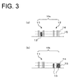
- Figs. 3(a) and 3(b) when noise 13 is mixed in the pulse trains 11, 12 and a signal convoluted with this noise 13 is input to the comparator 130, the noise 13 may be wrongly detected as pulses of the burst signal 10 unless the reference voltage Vth input to the comparator 130 is set appropriately.
- the used reference voltage Vth is a set value of a code 14, it is possible to decode to the basic data correctly without being affected by the noise 13.
- the noise 13 is judged as pulses and decoded to the basic data wrongly, or as the reproduced pattern does not match either of the pulse patterns shown in Figs. 2(a) and 2(b) , decoding fails. Consequently, in the decode unit 140, the information transmitted in the burst signal 10 cannot be decoded appropriately or decoded to wrong information.
- the reference voltage Vth used in determination threshold of presence or absence of pulses by the comparator 130 needs to be set appropriately.
- the information from the decode unit 140 is used as a basis to control the reference voltage Vth to be an appropriate value by the control unit 150. The method for controlling the reference voltage Vth in the pulse receiver 100 will be described below.
- the decode unit 140 decodes the pulse train 20 to the information 30 as described above, counts the number of decoding success for a predetermined time interval (count time Ts) and outputs the counted rate (decoding success rate DR) to the control unit 150.
- the decoding success rate counted at the decode unit 140 is the number of decoding success made for the count time Ts, irrespective of whether the decoded information is correct or not.
- the decoding success is such that the pulse train input from the comparator 130 is compared with the pulse patterns of basic data stored in advance as illustrated in Figs. 2(a), 2(b) and determined to coincide with the pulse pattern of basic data "1" or "0".
- the control unit 150 uses as a basis the decoding success rate DR communicated from the decode unit 140 to control the reference voltage used in the comparator 130.
- the control unit 150 receives the decoding success rate DR counted for the count time Ts from the decode unit 140 and uses it to calculate a set value of reference voltage Vth output to the comparator 130, which method will be described below.
- a target value of the decoding success rate DR suitable for decoding by the decode unit 140 is a decoding target rate DR TGT .
- Br denotes a data transfer rate.
- the decoding target rate DR TGT is 50000.
- the deviation Err obtained by the above-mentioned equation (2) is used to renew a set value of reference voltage Vth by the following equation (here, it is assumed below that the symbol Vth represents a reference voltage as an analog value supplied to the comparator 130 or a set value (reference voltage) as a target for renewal in the control unit 150, depending on the context).
- Vthnew Vth + P x Err + I x ⁇ Err
- Vthnew denotes a renewed set value of reference voltage
- Vth denotes a current set value of reference voltage before renewal.
- ⁇ Err is a cumulative value of deviation and P and I are preset constants, that is, a proportional control constant and an integral control constant.
- the equation (3) shows the set value of reference voltage Vth is renewed by a proportional component P x Err and an integral component I x ⁇ Err of the deviation Err.
- the set value Vth can be renewed to a suitable value smoothly and stably by setting the proportional control constant P and the integral control constant I appropriately.
- the renewed set value of reference voltage Vthnew which is renewed based on the equation (3) is output from the control unit 150 to the D/A converter 160, in which it is converted to an analog signal.
- This analog signal is output from the D/A converter 160 to the comparator 130 as the reference voltage Vth used in the comparator 130.
- Renewal of the set value of reference voltage Vth based on the equation (3) is repeated until the deviation Err becomes equal to or less than a first determination value P1.
- the set value of reference voltage Vth is controlled to be a suitable value, thereby making it possible to provide a preferable receiver with a minimized BER.
- the first determination value P1 is set to 0.
- the reference voltage Vth is renewed and controlled so as to prevent failure of decoding by the decode unit 140.
- a value corresponding to a greater positive voltage value as compared with the amplified (positive) burst signal to be input to the comparator 130 is input as an initial value of the reference voltage set value Vth and the proportional control constant P and the integral control constant I used in the equation (3) are both negative constants.
- the control unit 150 lowers the set value of reference voltage Vth gradually from the initial value thereby to control the deviation Err to be equal to or less than the first determination value P1.
- the initial value of the reference voltage set value Vth set in the comparator 130 is, for example, 250 mV (see Fig. 5 described later).
- Fig. 4 is a flowchart showing the flow of control performed by the control unit 150.
- an initial value is set to a parameter used in control by the control unit 150.
- a set value Vthmax corresponding to a predetermined greater voltage value is set as the initial value to the set value of reference voltage Vthnew output from the control unit 150 to the comparator 130 via the D/A converter 160.
- Vthmax is a set value corresponding to a greater positive reference voltage as compared with the amplified (positive) burst signal to be input to the comparator 130 as described above.
- the deviation Err and the integral value ⁇ Err are set to 0.
- step S2 it is determined whether the pulse receiver 100 is in communication or not. Determination whether it is in communication or not is performed by determining whether the burst signal 10 is received or not. When it is determined that the pulse receiver 100 is in communication, it goes to the next step S3. If it is determined that the pulse receiver 100 is not in communication, control is terminated.
- step S3 a finally renewed set value of reference voltage Vthnew is set to the current set value of reference voltage Vth and output to the D/A converter 160.
- step S4 the decoding success rate DR for the count time Ts is input from the decode unit 140 and in the step S5, the deviation Err is calculated by the equation (2).
- step S6 it is determined whether or not the deviation Err is equal to or less than the first determination value P1.
- the deviation Err is equal to or less than the determination value P1, it goes to the step S7.
- the deviation Err is greater than the determination value P1, it goes to the step S8.
- the step S7 it is assumed that the decoding success rate DR reaches the decoding target rate DR TGT and therefore, the integral value ⁇ Err of the deviation is reset to 0.
- the renewed value Vthnew of the reference voltage is calculated by the equation (3).
- the renewed set value of reference voltage Vthnew is output to the D/A converter 160 in the step S3 of the next cycle and output to the comparator 130 to be used in the reference voltage Vth.
- the deviation Err calculated in the step S5 is added to the integral value ⁇ Err of the deviation Err accumulated till then and the integral value ⁇ Err is renewed.
- the renewed integral value ⁇ Err is used in calculation of a renewed value of reference voltage Vthnew in the step S8 of the next cycle.
- the processing of the steps S2 to S9 is repeated until it is determined in the step S6 that the deviation Err is equal to or less than the first determination value P1.
- the reference voltage Vth is renewed and controlled such that the decoding success rate DR reaches the decoding target rate DR TGT. Consequently, it becomes possible to reduce the BER to the target value or less to decode the burst signal.
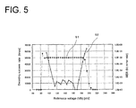
- BER and decoding success rate DR when the reference voltage Vth is set to various fixed values, instead of being renewed by the control unit 150, are shown in Fig. 5 .
- the BER denotes a ratio of the burst signal 10 which is not decoded to correct information.
- the decoding success rate DR includes the case of wrong decoding as a success and the BER includes both of the number of failed decoding and the number of wrong decoding.
- the decoding target rate DR TGT is 50000 and the decoding success rate DR is denoted by the reference numeral 51 and the BER is denoted by the reference numeral 52.
- the decoding success rate DR reaches the decoding target rate DR TGT .
- the pulse receiver 100 of the present embodiment it is possible to achieve an optimal BER for communication by setting the decoding target rate DR TGT appropriately and controlling the set value of reference voltage Vth by the control unit 150 in such a manner that the decoding success rate DR reaches the decoding target rate DR TGT.
- the pulse receiver of the present embodiment it is possible to achieve an optimal BER for reception based on a decoding state of a reception signal without need to add another signal or provide another reception circuit. With this structure, it is possible to provide a pulse receiver which is compact, low-cost and stable in pulse reception performance.
- the decoding success rate DR is lowered drastically at the reference voltage Vth of 80 mV or less. This means that noise cannot be processed appropriately when the reference voltage is too low. Besides, the decoding success rate DR is also lowered drastically at the reference voltage exceeding 185 mV. This means that the pulse signal contained in the burst signal cannot be detected when the reference voltage Vth is too high.
- the BER is optimized by lowering the reference voltage Vth sequentially from the high level Vthmax and further lowering the reference voltage Vth after the decoding success rate DR reaches the decoding target rate DR TGT at the reference voltage Vth of 185 mV.
- a predetermined positive offset voltage Voffset is further subtracted from the voltage obtained when the decoding success rate DR reaches the decoding target rate DR TGT .
- the offset voltage Voffset for example, 15 mV
- Fig. 6 is a flowchart showing the flow of control performed by the control unit 140.
- the processing performed when it is determined the deviation Err is equal to or less than the first determination value P1 in the step S6 is different from that in the first embodiment shown in the flowchart of Fig. 4 . That is, when it is determined in the step S6 that the deviation Err is equal to or less than the first determination value P1, it is then determined in the step S21 whether the integral value ⁇ Err of the deviation is equal to or less than a second determination value P2.
- the second determination value P2 is set to 0 or more.
- the processing is terminated without calculating of the renewed value Vthnew of the reference voltage by the control unit 150.
- the renewed value Vthnew used till then is not renewed further and output to the D/A converter 160 in the step S3.
- the positive offset voltage Voffset is subtracted from the reference voltage obtained in the first embodiment, which makes it possible to decode information with a smaller BER than that of the first embodiment.
- Fig. 7 illustrates comparison results of BER between use of the reference voltage calculated in the first embodiment from which the offset voltage Voffset is not subtracted and use of the reference voltage calculated in the second embodiment from which the offset voltage Voffset is subtracted.
- the horizontal axis indicates loss (attenuation amount) in the burst signal 10 in the transmission channel and the vertical axis indicates the BER.
- the BER when the reference voltage of the first embodiment is used is denoted by the reference numeral 61 and the BER when the reference voltage of the second embodiment is used is denoted by the reference numeral 62.
- the positive offset voltage Voffset subtracted in the second embodiment is 15 mV. As illustrated in Fig. 7 , the BER is reduced drastically when using the reference voltage of the second embodiment from which the offset voltage Voffset is subtracted, irrespective of loss in the burst signal 10 in the transmission channel.
- Variations of BER in accordance with the reception level of the burst signal 10 when the reception level is changed by varying the state of the transmission channel is shown in Fig. 8 by way of comparison between the case of the second embodiment applied and the case of the second embodiment not applied.
- a fixed value is used as the reference voltage Vth when the second embodiment is not applied.
- the reference numeral 70 denotes the BER when the second embodiment is applied and reference numerals 71 to 75 denote the BER when the reference voltages Vth is fixed to 120 mV, 160 mV, 180mV, 190 mV, 195 mV, respectively.
- the BER is reduced over a wide range of reception levels as compared with the case where any of these fixed values is used as reference voltage, and excellent decoding of the burst signal 10 is realized.
- the pulse receiver of this embodiment it is possible to achieve more preferable BER for reception than that in the first embodiment and there is no need to add another signal or provide another reception circuit. With this structure, it is possible to provide a pulse receiver which is compact size, low-cost and stable in pulse reception performance.
Landscapes
- Engineering & Computer Science (AREA)
- Computer Networks & Wireless Communication (AREA)
- Signal Processing (AREA)
- Power Engineering (AREA)
- Physics & Mathematics (AREA)
- Spectroscopy & Molecular Physics (AREA)
- Dc Digital Transmission (AREA)
- Circuits Of Receivers In General (AREA)
- Noise Elimination (AREA)
Abstract
Description
- The present invention relates to a pulse receiver which receives a burst signal composed of plural pulses and controls to realize an optimal state for demodulation, and also to a method for receiving such a burst signal.
- In a receiver used in wireless communications, any of the following signal processing methods are performed in order to keep the reception signal to a constant level.
- (1) Performing automatic gain control (AGC) on an amplifier in response to the reception level and keeping the input level of the reception signal to a demodulator constant (Patent Literature 1)
- (2) Adding a pilot signal different from a main signal in frequency and monitoring only the pilot signal thereby to perform the above-mentioned AGC (Non-Patent Literature 1).
- (3) Generating and transmitting a training signal with a unique word, receiving and demodulating the signal thereby to determine the bit error rate so as to control a threshold or AGC (Patent Literature 2).
- As to the above-mentioned (1), the system of controlling a variable attenuator in a reception signal input unit by monitoring an error rate correction degree of a reception demodulated signal or monitoring the reception level of a reception signal (baseband signal) so as to demodulate the reception signal in the radio receiver in s stable manner is disclosed in the
patent literature 1. Besides, as to the above-mentioned (2), the ADSL of determining a specific fixed frequency, for example, 276 kHz as a pilot frequency, monitoring the reception level of the specific frequency constantly thereby to estimate the transmission state of a main signal and controlling the reception level to be optimal according to need is disclosed in the non-patentliterature 1. Further, as for the above-mentioned (3), the system of inserting a pilot signal with a known unique word into a transmission signal periodically over plural periods by a transmitter, monitoring the pilot signal contained in a reception signal by a receiver and determining the reception state of the signal thereby to correct and demodulate the data is disclosed in thepatent literature 2. -
- PL1: Japanese Patent Application Laid-Open No.
1993(H05)-129862 - PL2: Japanese Patent Application Laid-Open No.
2000-059269 - NPL1: ITU-T G992.1 Asymmetrical Digital Subscriber Line (ADSL) Transceivers.
- However, the above-mentioned conventional systems of keeping the reception signal level constant are all premised on the continuous data transfer, and are systems of monitoring reception signal level continuously, inserting a pilot signal or a specific data pattern to monitor the reception level and bit error rate thereby to control the receiver optimally or correcting data. For example, in control of an AGC circuit disclosed in the
patent literature 1, it is necessary to detect the level of a reception signal and also to make highspeed control of the AGC circuit, and it is difficult in view of characteristics of the wave detector to detect the reception signal level of the burst signal that uses short pulses. - Besides, in the method disclosed in the
non-patent literature 1 of estimating a transmission state of a main signal by a pilot signal and controlling an amplifier and a threshold, it is necessary to monitor the pilot signal which is transmitted with a frequency different from that of the main signal, and a special monitoring circuit is required. - Further, in the system disclosed in the
patent literature 2 of inserting a unique word, transmitting by a transmitter and extracting the unique word by a receiver, it is necessary to insert the unique word repeatedly at a fixed time interval, which is not suitable for burst communication. - The present invention was carried out so as to solve the above-mentioned problems, and aims to provide a pulse receiver capable of receiving a burst signal and decoding the burst signal with a bit error rate minimized to a target value or less by controlling a determination threshold such that decoding success rate is equal to or greater than a predetermined value.
- In order to solve the above-mentioned problems, a first aspect of a pulse receiver of the present invention is a pulse receiver for receiving a burst signal containing information to transfer and decoding and outputting the information, comprising: a comparator provided for comparing the burst signal with a reference voltage and outputting a pulse train corresponding to the burst signal; a decode unit provided for receiving the pulse train from the comparator, decoding the pulse train to predetermined basic data sequentially and outputting the data as the information, and counting, for a predetermined count time, a decoding success rate which is a number of times of decoding of the pulse train to the basic data; and a control unit provided for receiving the decoding success rate from the decode unit, calculating a deviation by subtracting the decoding success rate from a predetermined decoding target rate, when the deviation is greater than a predetermined first determination value that is equal to or greater than 0, renewing a set value of the reference voltage so as to reduce the deviation and outputting the set value to the comparator, and repeating renewal of the set value of the reference voltage until the deviation becomes equal to or less than the first determination value.
- As the reference voltage of the comparator is renewed based on the deviation between the decoding target rate and the decoding success rate in such a manner as to lower the deviation, it is possible to reduce the bit error rate (BER) to the target value or less to decode the burst signal.
- A second aspect of the pulse receiver of the present invention is characterized in that, in the first aspect of the pulse receiver, when the deviation is greater than the first determination value, the control unit renews the set value by adding, to the set value, a proportional component obtained by multiplying the deviation by a predetermined proportional control constant and an integral component obtained by multiplying a cumulative value of the deviation by a predetermined integral control constant, and when the deviation is equal to or less than the first determination value and the cumulative value of the deviation is greater than a predetermined second determination value that is equal to or greater than 0, the control unit subtracts an offset value corresponding to an offset voltage from the set value and resets the cumulative value of the deviation to 0.
- As the set value of reference voltage is renewed with the proportional component and integral component of the deviation, it is possible to make the set value of reference voltage converge smoothly and stably and to reduce the BER more by use of the set value of reference voltage from which a predetermined offset voltage is subtracted.
- A third aspect of the pulse receiver of the present invention is characterized in that, in the first aspect of the pulse receiver, when the deviation is greater than the first determination value, the control unit renews the set value by adding, to the set value, a proportional component obtained by multiplying the deviation by a predetermined proportional control constant and an integral component obtained by multiplying a cumulative value of the deviation by a predetermined integral control constant.
- As the set value of reference voltage is renewed with the proportional component and integral component of the deviation, it is possible to make the set value of reference voltage converge smoothly and stably.
- A fourth aspect of the pulse receiver of the present invention is characterized in that, in the second aspect of the pulse receiver, the control unit sets, as an initial value, a set value of the reference voltage that is positive and greater as compared with the burst signal input to the comparator, the proportional control constant and the integral control constant are negative, and the offset voltage is positive.
- A fifth aspect of the pulse receiver of the present invention is characterized in that, in the third aspect of the pulse receiver, the control unit sets, as an initial value, a set value of the reference voltage that is positive and greater as compared with the burst signal input to the comparator, and the proportional control constant and the integral control constant are negative.
- A first aspect of a method for receiving a burst signal of the present invention is characterized by comprising: (a) receiving the burst signal containing information to transfer; (b) comparing the burst signal with a reference voltage and generating a pulse train corresponding to the burst signal; (c) decoding the pulse train to predetermined basic data sequentially and outputting the data as the information, and counting, for a predetermined count time, a decoding success rate which is a number of times of decoding of the pulse train to the basic data; and (d) calculating a deviation by subtracting the decoding success rate from a predetermined decoding target rate, when the deviation is greater than a predetermined first determination value that is equal to or greater than 0, renewing a set value of the reference voltage so as to reduce the deviation and setting the reference voltage to the set value, wherein the steps (a) to (d) are repeated until the deviation becomes equal to or less than the first determination value.
- A second aspect of the method for receiving a burst signal of the present invention is characterized in that, in the first aspect of the method for receiving a burst signal, in the step (d), when the deviation is greater than the first determination value, the set value is renewed by adding, to the set value, a proportional component obtained by multiplying the deviation by a predetermined proportional control constant and an integral component obtained by multiplying a cumulative value of the deviation by a predetermined integral control constant, and the method further comprises (e), when the deviation is equal to or less than the first determination value and the cumulative value of the deviation is greater than a predetermined second determination value that is equal to or greater than 0, subtracting an offset value corresponding to an offset voltage from the set value and resetting the cumulative value of the deviation to 0.
- A third aspect of the method for receiving a burst signal of the present invention is characterized in that, in the first aspect of the method for receiving a burst signal, in the step (d), when the deviation is greater than the first determination value, the set value is renewed by adding, to the set value, a proportional component obtained by multiplying the deviation by a predetermined proportional control constant and an integral component obtained by multiplying a cumulative value of the deviation by a predetermined integral control constant.
- A fourth aspect of the method for receiving a burst signal of the present invention is characterized in that, in the second aspect of the method for receiving a burst signal, a set value of the reference voltage that is positive and greater as compared with the burst signal is set as an initial value of the set value, the proportional control constant and the integral control constant are negative, and the offset voltage is positive.
- A fifth aspect of the method for receiving a burst signal of the present invention is characterized in that, in the third aspect of the method for receiving a burst signal, a set value of the reference voltage that is positive and greater as compared with the burst signal is set as an initial value of the set value, and the proportional control constant and the integral control constant are negative.
- According to the pulse receiver of the present invention, it is possible to receive a burst signal and decode the burst signal with a bit error rate reduced to a target value or less by controlling a determination threshold such that decoding success rate becomes equal to or greater than a predetermined value.
-
-
Fig. 1 is a block diagram illustrating the structure of a pulse receiver according to a first embodiment of the present invention; -
Figs. 2(a) and 2(b) are explanatory views illustrating an example of pulse pattern corresponding to basic data "1" and "0"; -
Figs. 3(a) and 3(b) are explanatory views illustrating an example where noise is mixed in a burst signal; -
Fig. 4 is a flowchart of control performed by a control unit of the first embodiment; -
Fig. 5 is a graph showing variations in BER (bit error rate) and decoding success rate when reference voltage is set to various fixed values; -
Fig. 6 is a flowchart of control performed by a control unit of a second embodiment; -
Fig. 7 is a graph showing comparison of BER between the reference voltage of the first embodiment and the reference voltage of the second embodiment; and -
Fig. 8 is a graph showing BER when the reception level of the burst signal varies. - With reference to the drawings, a pulse receiver according to a preferred embodiment of the present invention will be described in detail below. Elements having the like functions are denoted by the like reference numerals for simple illustration and description.
- A pulse receiver according to the first embodiment of the present invention will be described with reference to
Fig. 1. Fig. 1 is a block diagram illustrating the structure of thepulse receiver 100 of the present embodiment. Thepulse receiver 100 of this embodiment has a band-pass filter (BPF) 110, a low noise amplifier (LNA) 120, acomparator 130, adecode unit 140, acontrol unit 150 and a D/A converter 160. Aburst signal 10, which contains digital information and is sent from a transmitter (not shown) by wire or wireless communications, is affected by noise, attenuation and the like in a transmission channel and then, received by thepulse receiver 100 of this embodiment. - The
burst signal 10 received by thepulse receiver 100 contains a pulse train composed of plural pulses and the width of each pulse is several nanoseconds or less. Theburst signal 10 is subjected to pulse position modulation (PPM) in which information is modulated by positional relation of the pulse train. The burst signal is, for example, as illustrated inFigs 2(a) and 2(b) , composed of apulse pattern 10a corresponding to basic data "1" and apulse pattern 10b corresponding to basic data "0". - In
Figs. 2(a) and 2(b) , twopulse trains Fig. 2(a) , and only onepulse pattern 11 is assigned to the pulse pattern corresponding to the basic data "0" ofFig. 2(b) and no pulse train is assigned to the position corresponding to thepulse train 12 in the pulse pattern of the basic data "1". With this structure, thepulse train 11 is used as a reference and decoding to the basic data "1" or "0" is performed by determining whether thepulse train 12 exists at the predetermined position or not. Here, inFigs. 2(a) and 2(b) , it is assumed that thepulse trains - The
burst signal 10 received by thepulse receiver 100 is first input to theBPF 110, in which the band is restricted. Then, theburst signal 10 is output to the LNA 120. In the LNA 120, the signal output from the BPF 110 is amplified to a fixed level and output to thecomparator 130. In thecomparator 130, the signal input from theLNA 120 is compared with a reference voltage Vth. When the input signal exceeds the reference voltage Vth, a signal corresponding to "High" is output, while the signal is equal to or less than the reference voltage Vth, a signal corresponding to "Low" is output. In this way, thecomparator 130 outputs apulse train 20 corresponding to received wave profile. - The
pulse train 20 output from thecomparator 130 is input to thedecode unit 140, decoded to basic data "1" or "0" sequentially and output asinformation 30. InFig. 1 , thepulse receiver 100 is connected to a personal computer (PC) 1 as an external device and theinformation 30 output from thedecode unit 140 is output to thePC 1. Information of the pulse train which is not decoded to the basic data at thedecode unit 140 is not output to the external device. - In the
pulse receiver 100, in order for thedecode unit 140 to decode information appropriately, thepulse train 20 input from thecomparator 130 needs to be a precise reproduction of the receivedburst signal 10. Theburst signal 10 input to thepulse receiver 100 has pulse trains 11, 12 as illustrated inFigs. 2(a) and 2(b) . However, when it is affected by attenuation, noise and the like in the transmission channel before being received by thepulse receiver 100, the receivedburst signal 10 cannot be reproduced precisely by thecomparator 130. - For example, as illustrated in
Figs. 3(a) and 3(b) , whennoise 13 is mixed in the pulse trains 11, 12 and a signal convoluted with thisnoise 13 is input to thecomparator 130, thenoise 13 may be wrongly detected as pulses of theburst signal 10 unless the reference voltage Vth input to thecomparator 130 is set appropriately. In the example ofFigs. 3 (a) and 3(b) , when the used reference voltage Vth is a set value of acode 14, it is possible to decode to the basic data correctly without being affected by thenoise 13. However, when the used reference voltage Vth is a set value of acode 15, thenoise 13 is judged as pulses and decoded to the basic data wrongly, or as the reproduced pattern does not match either of the pulse patterns shown inFigs. 2(a) and 2(b) , decoding fails. Consequently, in thedecode unit 140, the information transmitted in theburst signal 10 cannot be decoded appropriately or decoded to wrong information. - As described above, in order for the
decode unit 140 to decode information transmitted in theburst signal 10 appropriately, the reference voltage Vth used in determination threshold of presence or absence of pulses by thecomparator 130 needs to be set appropriately. In thepulse receiver 100 of the present embodiment, the information from thedecode unit 140 is used as a basis to control the reference voltage Vth to be an appropriate value by thecontrol unit 150. The method for controlling the reference voltage Vth in thepulse receiver 100 will be described below. - The
decode unit 140 decodes thepulse train 20 to theinformation 30 as described above, counts the number of decoding success for a predetermined time interval (count time Ts) and outputs the counted rate (decoding success rate DR) to thecontrol unit 150. The decoding success rate counted at thedecode unit 140 is the number of decoding success made for the count time Ts, irrespective of whether the decoded information is correct or not. Here, the decoding success is such that the pulse train input from thecomparator 130 is compared with the pulse patterns of basic data stored in advance as illustrated inFigs. 2(a), 2(b) and determined to coincide with the pulse pattern of basic data "1" or "0". Therefore, wrong decoding such that the pulse pattern is wrongly decoded to "1" instead of "0" due to thenoise 13 or the like is regarded as decoding success and the decoding success rate is incremented. On the other hand, if the reproduced pulse pattern does not coincide with the pulse pattern of basic data stored in advance due to thenoise 13 or the like and cannot be decoded "1" nor "0", the decoding success rate is not incremented. - The
decode unit 140 counts the number of decoding successes mentioned above for the count time Ts (for example, Ts = 500 ms) and outputs it as the decoding success rate DR to thecontrol unit 150. Thecontrol unit 150 uses as a basis the decoding success rate DR communicated from thedecode unit 140 to control the reference voltage used in thecomparator 130. - The
control unit 150 receives the decoding success rate DR counted for the count time Ts from thedecode unit 140 and uses it to calculate a set value of reference voltage Vth output to thecomparator 130, which method will be described below. - It is assumed that a target value of the decoding success rate DR suitable for decoding by the
decode unit 140 is a decoding target rate DRTGT. The decoding target rate DRTGT is expressed by the following equation.
- Here, Br denotes a data transfer rate. As an example, when the data transfer rate Br is 100 kbps and the count time Ts is 500 ms, the decoding target rate DRTGT is 50000.
- Here, it is assumed that a difference between the above-mentioned decoding target rate DRTGT and a decoding success rate DR counted by the
decode unit 140 is a deviation Err. The deviation Err is obtained by the following equation.
- In the
control unit 150, the deviation Err obtained by the above-mentioned equation (2) is used to renew a set value of reference voltage Vth by the following equation (here, it is assumed below that the symbol Vth represents a reference voltage as an analog value supplied to thecomparator 130 or a set value (reference voltage) as a target for renewal in thecontrol unit 150, depending on the context).
Here, Vthnew denotes a renewed set value of reference voltage and Vth denotes a current set value of reference voltage before renewal. And, ∑Err is a cumulative value of deviation and P and I are preset constants, that is, a proportional control constant and an integral control constant. - The equation (3) shows the set value of reference voltage Vth is renewed by a proportional component P x Err and an integral component I x ∑Err of the deviation Err. In renewal of the reference voltage set value Vth based on the equation (3), the set value Vth can be renewed to a suitable value smoothly and stably by setting the proportional control constant P and the integral control constant I appropriately.
- The renewed set value of reference voltage Vthnew which is renewed based on the equation (3) is output from the
control unit 150 to the D/A converter 160, in which it is converted to an analog signal. This analog signal is output from the D/A converter 160 to thecomparator 130 as the reference voltage Vth used in thecomparator 130. - Renewal of the set value of reference voltage Vth based on the equation (3) is repeated until the deviation Err becomes equal to or less than a first determination value P1. With this repetition, the set value of reference voltage Vth is controlled to be a suitable value, thereby making it possible to provide a preferable receiver with a minimized BER. As a preferable example, the first determination value P1 is set to 0. In this case, the reference voltage Vth is renewed and controlled so as to prevent failure of decoding by the
decode unit 140. - Preferably, a value corresponding to a greater positive voltage value as compared with the amplified (positive) burst signal to be input to the
comparator 130 is input as an initial value of the reference voltage set value Vth and the proportional control constant P and the integral control constant I used in the equation (3) are both negative constants. With this setting, thecontrol unit 150 lowers the set value of reference voltage Vth gradually from the initial value thereby to control the deviation Err to be equal to or less than the first determination value P1. The initial value of the reference voltage set value Vth set in thecomparator 130 is, for example, 250 mV (seeFig. 5 described later). - In the
pulse receiver 100 of this embodiment, the flow of control of thecontrol unit 150 for renewing the reference voltage Vth used in thecomparator 130 is explained with reference toFig. 4. Fig. 4 is a flowchart showing the flow of control performed by thecontrol unit 150. - First in the step S1, an initial value is set to a parameter used in control by the
control unit 150. First, a set value Vthmax corresponding to a predetermined greater voltage value is set as the initial value to the set value of reference voltage Vthnew output from thecontrol unit 150 to thecomparator 130 via the D/A converter 160. Vthmax is a set value corresponding to a greater positive reference voltage as compared with the amplified (positive) burst signal to be input to thecomparator 130 as described above. Besides, the deviation Err and the integral value ∑Err are set to 0. - In the step S2, it is determined whether the
pulse receiver 100 is in communication or not. Determination whether it is in communication or not is performed by determining whether theburst signal 10 is received or not. When it is determined that thepulse receiver 100 is in communication, it goes to the next step S3. If it is determined that thepulse receiver 100 is not in communication, control is terminated. - In the step S3, a finally renewed set value of reference voltage Vthnew is set to the current set value of reference voltage Vth and output to the D/
A converter 160. In the step S4, the decoding success rate DR for the count time Ts is input from thedecode unit 140 and in the step S5, the deviation Err is calculated by the equation (2). - In the step S6, it is determined whether or not the deviation Err is equal to or less than the first determination value P1. When the deviation Err is equal to or less than the determination value P1, it goes to the step S7. When the deviation Err is greater than the determination value P1, it goes to the step S8. In the step S7, it is assumed that the decoding success rate DR reaches the decoding target rate DRTGT and therefore, the integral value ∑Err of the deviation is reset to 0.
- When the process goes to the step S8, the renewed value Vthnew of the reference voltage is calculated by the equation (3). The renewed set value of reference voltage Vthnew is output to the D/
A converter 160 in the step S3 of the next cycle and output to thecomparator 130 to be used in the reference voltage Vth. In the step S9, the deviation Err calculated in the step S5 is added to the integral value ∑Err of the deviation Err accumulated till then and the integral value ∑Err is renewed. The renewed integral value ∑Err is used in calculation of a renewed value of reference voltage Vthnew in the step S8 of the next cycle. - In the flowchart of
Fig. 4 , the processing of the steps S2 to S9 is repeated until it is determined in the step S6 that the deviation Err is equal to or less than the first determination value P1. With this repetition, the reference voltage Vth is renewed and controlled such that the decoding success rate DR reaches the decoding target rate DRTGT. Consequently, it becomes possible to reduce the BER to the target value or less to decode the burst signal. - In the
pulse receiver 100, variations of BER and decoding success rate DR when the reference voltage Vth is set to various fixed values, instead of being renewed by thecontrol unit 150, are shown inFig. 5 . Here, the BER denotes a ratio of theburst signal 10 which is not decoded to correct information. The decoding success rate DR includes the case of wrong decoding as a success and the BER includes both of the number of failed decoding and the number of wrong decoding. InFig. 5 , it is assumed that the decoding target rate DRTGT is 50000 and the decoding success rate DR is denoted by thereference numeral 51 and the BER is denoted by thereference numeral 52. - As seen from
Fig. 5 , when the reference voltage Vth is equal to or less than 185 mV, the decoding success rate DR reaches the decoding target rate DRTGT. Besides, it is also seen that the BER can be optimized (BER = about 10-3 or less) required for excellent communication when the reference voltage Vth is 185 mV or less. - As described above, in the
pulse receiver 100 of the present embodiment, it is possible to achieve an optimal BER for communication by setting the decoding target rate DRTGT appropriately and controlling the set value of reference voltage Vth by thecontrol unit 150 in such a manner that the decoding success rate DR reaches the decoding target rate DRTGT. In the pulse receiver of the present embodiment, it is possible to achieve an optimal BER for reception based on a decoding state of a reception signal without need to add another signal or provide another reception circuit. With this structure, it is possible to provide a pulse receiver which is compact, low-cost and stable in pulse reception performance. - Here, the decoding success rate DR is lowered drastically at the reference voltage Vth of 80 mV or less. This means that noise cannot be processed appropriately when the reference voltage is too low. Besides, the decoding success rate DR is also lowered drastically at the reference voltage exceeding 185 mV. This means that the pulse signal contained in the burst signal cannot be detected when the reference voltage Vth is too high.
- The structure of a pulse receiver according to a second embodiment of the present invention will be described below. As seen from
Fig. 5 , the BER is optimized by lowering the reference voltage Vth sequentially from the high level Vthmax and further lowering the reference voltage Vth after the decoding success rate DR reaches the decoding target rate DRTGT at the reference voltage Vth of 185 mV. - Then, in the present embodiment, a predetermined positive offset voltage Voffset is further subtracted from the voltage obtained when the decoding success rate DR reaches the decoding target rate DRTGT. In the example shown in
Fig. 5 , the offset voltage Voffset, for example, 15 mV, is subtracted from the voltage 185 mV obtained when the decoding success rate DR reaches the decoding target rate DRTGT, and the reference voltage Vth 170 mV is obtained. Then, the BER is a value (BER = about 10-6 or less) which is sufficiently lower than the value required for excellent communication (BER = about 10-3 or less). Here, there is no need to subtract the offset voltage Voffset when the decoding success rate DR reaches the decoding target rate DRTGT and the integral value ∑Err of the deviation is sufficiently low (equal to or less than a second determination value P2 described later). - The flow of processing of the
control unit 150 in the second embodiment will be described with reference toFig. 6. Fig. 6 is a flowchart showing the flow of control performed by thecontrol unit 140. In this embodiment, the processing performed when it is determined the deviation Err is equal to or less than the first determination value P1 in the step S6 is different from that in the first embodiment shown in the flowchart ofFig. 4 . That is, when it is determined in the step S6 that the deviation Err is equal to or less than the first determination value P1, it is then determined in the step S21 whether the integral value ∑Err of the deviation is equal to or less than a second determination value P2. Here, the second determination value P2 is set to 0 or more. - When in the step S21, it is determined that the integral value ∑Err of the deviation is equal to or less than the second determination value P2, the processing is terminated without calculating of the renewed value Vthnew of the reference voltage by the
control unit 150. In this case, the renewed value Vthnew used till then is not renewed further and output to the D/A converter 160 in the step S3. - On the other hand, when it is determined that the integral value ∑Err of the deviation is greater than the second determination value P2, the integral value ∑Err of the deviation is reset to 0 in the step S22 and the set value of reference voltage is renewed by the following equation in the step S23.

This reference voltage Vthnew is output to the D/A converter in the step S3 and set and used in thecomparator 130. - As described above, in the second embodiment, the positive offset voltage Voffset is subtracted from the reference voltage obtained in the first embodiment, which makes it possible to decode information with a smaller BER than that of the first embodiment.
Fig. 7 illustrates comparison results of BER between use of the reference voltage calculated in the first embodiment from which the offset voltage Voffset is not subtracted and use of the reference voltage calculated in the second embodiment from which the offset voltage Voffset is subtracted. - In
Fig. 7 , the horizontal axis indicates loss (attenuation amount) in theburst signal 10 in the transmission channel and the vertical axis indicates the BER. The BER when the reference voltage of the first embodiment is used is denoted by thereference numeral 61 and the BER when the reference voltage of the second embodiment is used is denoted by thereference numeral 62. Besides, the positive offset voltage Voffset subtracted in the second embodiment is 15 mV. As illustrated inFig. 7 , the BER is reduced drastically when using the reference voltage of the second embodiment from which the offset voltage Voffset is subtracted, irrespective of loss in theburst signal 10 in the transmission channel. - Variations of BER in accordance with the reception level of the
burst signal 10 when the reception level is changed by varying the state of the transmission channel is shown inFig. 8 by way of comparison between the case of the second embodiment applied and the case of the second embodiment not applied. Here, a fixed value is used as the reference voltage Vth when the second embodiment is not applied. InFig. 8 , thereference numeral 70 denotes the BER when the second embodiment is applied andreference numerals 71 to 75 denote the BER when the reference voltages Vth is fixed to 120 mV, 160 mV, 180mV, 190 mV, 195 mV, respectively. As seen fromFig. 8 , when the second embodiment is applied, the BER is reduced over a wide range of reception levels as compared with the case where any of these fixed values is used as reference voltage, and excellent decoding of theburst signal 10 is realized. - As described above, in the second embodiment, as the positive offset voltage Voffset is subtracted from the reference voltage such that the decoding success rate DR reaches the decoding target rate DRTGT, it is possible to reduce the BER more. In the pulse receiver of this embodiment, it is possible to achieve more preferable BER for reception than that in the first embodiment and there is no need to add another signal or provide another reception circuit. With this structure, it is possible to provide a pulse receiver which is compact size, low-cost and stable in pulse reception performance.
- Here, the embodiments have been described by way of example of the pulse receiver of the present invention and are not limited to this example. The detail structure and operations of the pulse receiver according to the embodiments may be modified appropriately without departing from the scope of the present invention.
-
- 100
- pulse receiver
- 110
- band-pass filter
- 120
- low noise amplifier
- 130
- comparator
- 140
- decode unit
- 150
- control unit
- 160
- D/A converter
Claims (10)
- A pulse receiver for receiving a burst signal containing information to transfer and decoding and outputting the information, comprising:a comparator provided for comparing the burst signal with a reference voltage and outputting a pulse train corresponding to the burst signal;a decode unit provided for receiving the pulse train from the comparator, decoding the pulse train to predetermined basic data sequentially and outputting the data as the information, and counting, for a predetermined count time, a decoding success rate which is a number of times of decoding of the pulse train to the basic data; anda control unit provided for receiving the decoding success rate from the decode unit, calculating a deviation by subtracting the decoding success rate from a predetermined decoding target rate, when the deviation is greater than a predetermined first determination value that is equal to or greater than 0, renewing a set value of the reference voltage so as to reduce the deviation and outputting the set value to the comparator, and repeating renewal of the set value of the reference voltage until the deviation becomes equal to or less than the first determination value.
- The pulse receiver of claim 1, wherein,
when the deviation is greater than the first determination value, the control unit renews the set value by adding, to the set value, a proportional component obtained by multiplying the deviation by a predetermined proportional control constant and an integral component obtained by multiplying a cumulative value of the deviation by a predetermined integral control constant, and
when the deviation is equal to or less than the first determination value and the cumulative value of the deviation is greater than a predetermined second determination value that is equal to or greater than 0, the control unit subtracts an offset value corresponding to an offset voltage from the set value and resets the cumulative value of the deviation to 0. - The pulse receiver of claim 1, wherein, when the deviation is greater than the first determination value, the control unit renews the set value by adding, to the set value, a proportional component obtained by multiplying the deviation by a predetermined proportional control constant and an integral component obtained by multiplying a cumulative value of the deviation by a predetermined integral control constant.
- The pulse receiver of claim 2, wherein the control unit sets, as an initial value, a set value of the reference voltage that is positive and greater as compared with the burst signal input to the comparator, the proportional control constant and the integral control constant are negative, and the offset voltage is positive.
- The pulse receiver of claim 3, wherein the control unit sets, as an initial value, a set value of the reference voltage that is positive and greater as compared with the burst signal input to the comparator, and the proportional control constant and the integral control constant are negative.
- A method for receiving a burst signal, comprising:(a) receiving the burst signal containing information to transfer;(b) comparing the burst signal with a reference voltage and generating a pulse train corresponding to the burst signal;(c) decoding the pulse train to predetermined basic data sequentially and outputting the data as the information, and counting, for a predetermined count time, a decoding success rate which is a number of times of decoding of the pulse train to the basic data; and(d) calculating a deviation by subtracting the decoding success rate from a predetermined decoding target rate, when the deviation is greater than a predetermined first determination value that is equal to or greater than 0, renewing a set value of the reference voltage so as to reduce the deviation and setting the reference voltage to the set value,wherein the steps (a) to (d) are repeated until the deviation becomes equal to or less than the first determination value.
- The method of claim 6, wherein,
in the step (d), when the deviation is greater than the first determination value, the set value is renewed by adding, to the set value, a proportional component obtained by multiplying the deviation by a predetermined proportional control constant and an integral component obtained by multiplying a cumulative value of the deviation by a predetermined integral control constant, and
the method further comprises (e), when the deviation is equal to or less than the first determination value and the cumulative value of the deviation is greater than a predetermined second determination value that is equal to or greater than 0, subtracting an offset value corresponding to an offset voltage from the set value and resetting the cumulative value of the deviation to 0. - The method of claim 6, wherein,
in the step (d), when the deviation is greater than the first determination value, the set value is renewed by adding, to the set value, a proportional component obtained by multiplying the deviation by a predetermined proportional control constant and an integral component obtained by multiplying a cumulative value of the deviation by a predetermined integral control constant. - The method of claim 7, wherein a set value of the reference voltage that is positive and greater as compared with the burst signal is set as an initial value of the set value, the proportional control constant and the integral control constant are negative, and the offset voltage is positive.
- The method of claim 8, wherein a set value of the reference voltage that is positive and greater as compared with the burst signal is set as an initial value of the set value, and the proportional control constant and the integral control constant are negative.
Applications Claiming Priority (2)
| Application Number | Priority Date | Filing Date | Title |
|---|---|---|---|
| JP2010034548 | 2010-02-19 | ||
| PCT/JP2011/053173 WO2011102351A1 (en) | 2010-02-19 | 2011-02-15 | Pulse receiver and burst signal receiving method |
Publications (2)
| Publication Number | Publication Date |
|---|---|
| EP2538565A1 true EP2538565A1 (en) | 2012-12-26 |
| EP2538565A4 EP2538565A4 (en) | 2017-08-02 |
Family
ID=44482936
Family Applications (1)
| Application Number | Title | Priority Date | Filing Date |
|---|---|---|---|
| EP11744637.7A Withdrawn EP2538565A4 (en) | 2010-02-19 | 2011-02-15 | Pulse receiver and burst signal receiving method |
Country Status (5)
| Country | Link |
|---|---|
| US (1) | US8897396B2 (en) |
| EP (1) | EP2538565A4 (en) |
| JP (1) | JP5653995B2 (en) |
| CN (1) | CN102754349B (en) |
| WO (1) | WO2011102351A1 (en) |
Families Citing this family (2)
| Publication number | Priority date | Publication date | Assignee | Title |
|---|---|---|---|---|
| CN105007094B (en) * | 2015-07-16 | 2017-05-31 | 北京中宸泓昌科技有限公司 | A kind of exponent pair spread spectrum coding coding/decoding method |
| JP6955505B2 (en) * | 2016-03-08 | 2021-10-27 | クアン−チー インテリジェント フォトニック テクノロジー リミテッド | Optical noise elimination electric circuit, optical receiver and optical chip |
Family Cites Families (20)
| Publication number | Priority date | Publication date | Assignee | Title |
|---|---|---|---|---|
| US4145743A (en) * | 1976-12-27 | 1979-03-20 | Rca Corporation | Voltage level generator using digital integration |
| JPS57170652A (en) * | 1981-04-15 | 1982-10-20 | Nec Corp | Transmitting system for burst signal |
| GB2136248A (en) * | 1983-02-25 | 1984-09-12 | Philips Electronic Associated | Text error correction in digital data transmission systems |
| JP2530904B2 (en) * | 1988-02-22 | 1996-09-04 | 富士通株式会社 | Optimal discrimination level control method |
| FR2663483A1 (en) * | 1990-06-19 | 1991-12-20 | Portenseigne Radiotechnique | METHOD OF ADJUSTING A THRESHOLD DECODER FOR A MULTIPLE LEVEL SIGNAL AND TELEVISION RECEIVER PROVIDED WITH SUCH A DECODER. |
| JP3218474B2 (en) | 1991-10-31 | 2001-10-15 | 日本電気エンジニアリング株式会社 | AGC circuit for reception |
| US5781588A (en) * | 1994-11-10 | 1998-07-14 | Matsushita Electric Industrial Co., Ltd. | FSK signal receiver |
| JPH0983580A (en) * | 1995-09-12 | 1997-03-28 | Fujitsu Ltd | Automatic reference voltage setting circuit |
| JPH10164147A (en) * | 1996-11-26 | 1998-06-19 | Nitsuko Corp | System for adjusting data reception characteristic |
| JP3029030B2 (en) | 1998-08-05 | 2000-04-04 | 日本電気株式会社 | Method and apparatus for demodulating received signal including pilot signal |
| JP4019555B2 (en) * | 1999-05-25 | 2007-12-12 | Kddi株式会社 | Optical receiving apparatus and method |
| US7173551B2 (en) * | 2000-12-21 | 2007-02-06 | Quellan, Inc. | Increasing data throughput in optical fiber transmission systems |
| WO2002082694A1 (en) * | 2001-04-04 | 2002-10-17 | Quellan, Inc. | Method and system for decoding multilevel signals |
| JP4449259B2 (en) * | 2001-06-19 | 2010-04-14 | 日本電気株式会社 | AFC circuit |
| JP4105723B2 (en) * | 2003-08-05 | 2008-06-25 | 富士通株式会社 | Regenerative relay method and apparatus |
| JP2006261826A (en) * | 2005-03-15 | 2006-09-28 | Matsushita Electric Ind Co Ltd | Receiving apparatus and receiving method |
| KR100826882B1 (en) * | 2005-12-05 | 2008-05-06 | 한국전자통신연구원 | Digital automatic gain controller method and apparatus in bust mode optical receiver |
| US8024644B2 (en) * | 2006-11-14 | 2011-09-20 | Via Telecom Co., Ltd. | Communication signal decoding |
| KR20080084148A (en) * | 2007-03-15 | 2008-09-19 | 삼성전자주식회사 | Method and apparatus for decoding data in receiver of digital broadcasting system |
| CN101355389A (en) * | 2008-09-11 | 2009-01-28 | 中兴通讯股份有限公司 | A method and device for optimally adjusting receiver decision level |
-
2011
- 2011-02-15 WO PCT/JP2011/053173 patent/WO2011102351A1/en not_active Ceased
- 2011-02-15 EP EP11744637.7A patent/EP2538565A4/en not_active Withdrawn
- 2011-02-15 JP JP2012500605A patent/JP5653995B2/en not_active Expired - Fee Related
- 2011-02-15 CN CN201180008586.0A patent/CN102754349B/en not_active Expired - Fee Related
-
2012
- 2012-08-15 US US13/586,254 patent/US8897396B2/en not_active Expired - Fee Related
Non-Patent Citations (1)
| Title |
|---|
| See references of WO2011102351A1 * |
Also Published As
| Publication number | Publication date |
|---|---|
| US8897396B2 (en) | 2014-11-25 |
| CN102754349B (en) | 2014-11-19 |
| JPWO2011102351A1 (en) | 2013-06-17 |
| CN102754349A (en) | 2012-10-24 |
| WO2011102351A1 (en) | 2011-08-25 |
| US20120307940A1 (en) | 2012-12-06 |
| JP5653995B2 (en) | 2015-01-14 |
| EP2538565A4 (en) | 2017-08-02 |
Similar Documents
| Publication | Publication Date | Title |
|---|---|---|
| KR101183405B1 (en) | System and method of puncturing pulses in a receiver or transmitter | |
| US20020054583A1 (en) | Automatic gain control for a time division duplex receiver | |
| RU99124761A (en) | METHOD AND DEVICE FOR CONTROLLING TRANSMISSION POWER IN A COMMUNICATION SYSTEM | |
| CN105553616B (en) | Channel quality indicates selection method, adaptive modulation coding method and device | |
| EP3185430A1 (en) | Power-line carrier communication method | |
| EP0701334A2 (en) | Method and device to measure the impulse response of a radio channel | |
| EP1128572B1 (en) | A method of adjusting a signal quality target during transmission power control in a CDMA radio communication network | |
| EP1488553B1 (en) | Method, arrangement and communication receiver for snir estimation | |
| EP1265389A2 (en) | Method of impairment mitigation in a communication system | |
| US8897396B2 (en) | Pulse receiver and method for receiving burst signal | |
| JP5949297B2 (en) | Transmission power control method and mobile communication terminal device | |
| ATE314757T1 (en) | INTERFERENCE CANCELATION SYSTEM USING INDEPENDENT RECEIVER | |
| JP6669852B2 (en) | Method, apparatus and system for determining a scanning instant at a receiver | |
| CN101378288A (en) | Device for estimating offset | |
| US7515658B2 (en) | Method to adaptively scale the input to a channel decoder | |
| US9736709B2 (en) | Receiver with frequency deviation detection capability and method therefor | |
| CN101138189B (en) | Method and apparatus for signal quality estimation | |
| US8855701B2 (en) | Dynamic transmission power control method | |
| CN1985453A (en) | Wireless communication equipment and wireless communication method | |
| CN103716271A (en) | Adaptive detector threshold compensation in binary frame based communication systems | |
| US20070217484A1 (en) | Method for decoding digital data in a frequency hopping communication system | |
| JP2005236766A (en) | Transmission signal generating apparatus, radio base station, automatic gain control method and radio signal transmission method | |
| JP4800886B2 (en) | Receiving apparatus and receiving method | |
| JP5903620B2 (en) | Communication performance checker | |
| CN112422172B (en) | Automatic gain control method for monitoring uplink signal of broadband satellite communication |
Legal Events
| Date | Code | Title | Description |
|---|---|---|---|
| PUAI | Public reference made under article 153(3) epc to a published international application that has entered the european phase |
Free format text: ORIGINAL CODE: 0009012 |
|
| 17P | Request for examination filed |
Effective date: 20120816 |
|
| AK | Designated contracting states |
Kind code of ref document: A1 Designated state(s): AL AT BE BG CH CY CZ DE DK EE ES FI FR GB GR HR HU IE IS IT LI LT LU LV MC MK MT NL NO PL PT RO RS SE SI SK SM TR |
|
| DAX | Request for extension of the european patent (deleted) | ||
| RA4 | Supplementary search report drawn up and despatched (corrected) |
Effective date: 20170704 |
|
| RIC1 | Information provided on ipc code assigned before grant |
Ipc: H04B 1/7163 20110101AFI20170626BHEP Ipc: H04L 25/49 20060101ALI20170626BHEP Ipc: H04L 25/06 20060101ALI20170626BHEP |
|
| STAA | Information on the status of an ep patent application or granted ep patent |
Free format text: STATUS: THE APPLICATION HAS BEEN WITHDRAWN |
|
| 18W | Application withdrawn |
Effective date: 20171228 |