EP2538505A2 - System and method for suppressing parasitics in an optical device - Google Patents
System and method for suppressing parasitics in an optical device Download PDFInfo
- Publication number
- EP2538505A2 EP2538505A2 EP12161364A EP12161364A EP2538505A2 EP 2538505 A2 EP2538505 A2 EP 2538505A2 EP 12161364 A EP12161364 A EP 12161364A EP 12161364 A EP12161364 A EP 12161364A EP 2538505 A2 EP2538505 A2 EP 2538505A2
- Authority
- EP
- European Patent Office
- Prior art keywords
- ions
- wavelength
- energy
- core region
- laser
- Prior art date
- Legal status (The legal status is an assumption and is not a legal conclusion. Google has not performed a legal analysis and makes no representation as to the accuracy of the status listed.)
- Granted
Links
Images



Classifications
-
- H—ELECTRICITY
- H01—ELECTRIC ELEMENTS
- H01S—DEVICES USING THE PROCESS OF LIGHT AMPLIFICATION BY STIMULATED EMISSION OF RADIATION [LASER] TO AMPLIFY OR GENERATE LIGHT; DEVICES USING STIMULATED EMISSION OF ELECTROMAGNETIC RADIATION IN WAVE RANGES OTHER THAN OPTICAL
- H01S3/00—Lasers, i.e. devices using stimulated emission of electromagnetic radiation in the infrared, visible or ultraviolet wave range
- H01S3/05—Construction or shape of optical resonators; Accommodation of active medium therein; Shape of active medium
- H01S3/06—Construction or shape of active medium
- H01S3/0602—Crystal lasers or glass lasers
- H01S3/0612—Non-homogeneous structure
-
- H—ELECTRICITY
- H01—ELECTRIC ELEMENTS
- H01S—DEVICES USING THE PROCESS OF LIGHT AMPLIFICATION BY STIMULATED EMISSION OF RADIATION [LASER] TO AMPLIFY OR GENERATE LIGHT; DEVICES USING STIMULATED EMISSION OF ELECTROMAGNETIC RADIATION IN WAVE RANGES OTHER THAN OPTICAL
- H01S3/00—Lasers, i.e. devices using stimulated emission of electromagnetic radiation in the infrared, visible or ultraviolet wave range
- H01S3/09—Processes or apparatus for excitation, e.g. pumping
- H01S3/091—Processes or apparatus for excitation, e.g. pumping using optical pumping
- H01S3/094—Processes or apparatus for excitation, e.g. pumping using optical pumping by coherent light
- H01S3/09403—Cross-pumping, e.g. Förster process involving intermediate medium for excitation transfer
-
- H—ELECTRICITY
- H01—ELECTRIC ELEMENTS
- H01S—DEVICES USING THE PROCESS OF LIGHT AMPLIFICATION BY STIMULATED EMISSION OF RADIATION [LASER] TO AMPLIFY OR GENERATE LIGHT; DEVICES USING STIMULATED EMISSION OF ELECTROMAGNETIC RADIATION IN WAVE RANGES OTHER THAN OPTICAL
- H01S3/00—Lasers, i.e. devices using stimulated emission of electromagnetic radiation in the infrared, visible or ultraviolet wave range
- H01S3/14—Lasers, i.e. devices using stimulated emission of electromagnetic radiation in the infrared, visible or ultraviolet wave range characterised by the material used as the active medium
- H01S3/16—Solid materials
- H01S3/1691—Solid materials characterised by additives / sensitisers / promoters as further dopants
- H01S3/1698—Solid materials characterised by additives / sensitisers / promoters as further dopants rare earth
-
- H—ELECTRICITY
- H01—ELECTRIC ELEMENTS
- H01S—DEVICES USING THE PROCESS OF LIGHT AMPLIFICATION BY STIMULATED EMISSION OF RADIATION [LASER] TO AMPLIFY OR GENERATE LIGHT; DEVICES USING STIMULATED EMISSION OF ELECTROMAGNETIC RADIATION IN WAVE RANGES OTHER THAN OPTICAL
- H01S2301/00—Functional characteristics
- H01S2301/02—ASE (amplified spontaneous emission), noise; Reduction thereof
-
- H—ELECTRICITY
- H01—ELECTRIC ELEMENTS
- H01S—DEVICES USING THE PROCESS OF LIGHT AMPLIFICATION BY STIMULATED EMISSION OF RADIATION [LASER] TO AMPLIFY OR GENERATE LIGHT; DEVICES USING STIMULATED EMISSION OF ELECTROMAGNETIC RADIATION IN WAVE RANGES OTHER THAN OPTICAL
- H01S3/00—Lasers, i.e. devices using stimulated emission of electromagnetic radiation in the infrared, visible or ultraviolet wave range
- H01S3/05—Construction or shape of optical resonators; Accommodation of active medium therein; Shape of active medium
- H01S3/06—Construction or shape of active medium
- H01S3/0602—Crystal lasers or glass lasers
- H01S3/0606—Crystal lasers or glass lasers with polygonal cross-section, e.g. slab, prism
-
- H—ELECTRICITY
- H01—ELECTRIC ELEMENTS
- H01S—DEVICES USING THE PROCESS OF LIGHT AMPLIFICATION BY STIMULATED EMISSION OF RADIATION [LASER] TO AMPLIFY OR GENERATE LIGHT; DEVICES USING STIMULATED EMISSION OF ELECTROMAGNETIC RADIATION IN WAVE RANGES OTHER THAN OPTICAL
- H01S3/00—Lasers, i.e. devices using stimulated emission of electromagnetic radiation in the infrared, visible or ultraviolet wave range
- H01S3/05—Construction or shape of optical resonators; Accommodation of active medium therein; Shape of active medium
- H01S3/06—Construction or shape of active medium
- H01S3/063—Waveguide lasers, i.e. whereby the dimensions of the waveguide are of the order of the light wavelength
- H01S3/067—Fibre lasers
- H01S3/06708—Constructional details of the fibre, e.g. compositions, cross-section, shape or tapering
- H01S3/0672—Non-uniform radial doping
-
- H—ELECTRICITY
- H01—ELECTRIC ELEMENTS
- H01S—DEVICES USING THE PROCESS OF LIGHT AMPLIFICATION BY STIMULATED EMISSION OF RADIATION [LASER] TO AMPLIFY OR GENERATE LIGHT; DEVICES USING STIMULATED EMISSION OF ELECTROMAGNETIC RADIATION IN WAVE RANGES OTHER THAN OPTICAL
- H01S3/00—Lasers, i.e. devices using stimulated emission of electromagnetic radiation in the infrared, visible or ultraviolet wave range
- H01S3/14—Lasers, i.e. devices using stimulated emission of electromagnetic radiation in the infrared, visible or ultraviolet wave range characterised by the material used as the active medium
- H01S3/16—Solid materials
- H01S3/1601—Solid materials characterised by an active (lasing) ion
- H01S3/1603—Solid materials characterised by an active (lasing) ion rare earth
- H01S3/1608—Solid materials characterised by an active (lasing) ion rare earth erbium
-
- H—ELECTRICITY
- H01—ELECTRIC ELEMENTS
- H01S—DEVICES USING THE PROCESS OF LIGHT AMPLIFICATION BY STIMULATED EMISSION OF RADIATION [LASER] TO AMPLIFY OR GENERATE LIGHT; DEVICES USING STIMULATED EMISSION OF ELECTROMAGNETIC RADIATION IN WAVE RANGES OTHER THAN OPTICAL
- H01S3/00—Lasers, i.e. devices using stimulated emission of electromagnetic radiation in the infrared, visible or ultraviolet wave range
- H01S3/14—Lasers, i.e. devices using stimulated emission of electromagnetic radiation in the infrared, visible or ultraviolet wave range characterised by the material used as the active medium
- H01S3/16—Solid materials
- H01S3/1601—Solid materials characterised by an active (lasing) ion
- H01S3/1603—Solid materials characterised by an active (lasing) ion rare earth
- H01S3/1618—Solid materials characterised by an active (lasing) ion rare earth ytterbium
-
- H—ELECTRICITY
- H01—ELECTRIC ELEMENTS
- H01S—DEVICES USING THE PROCESS OF LIGHT AMPLIFICATION BY STIMULATED EMISSION OF RADIATION [LASER] TO AMPLIFY OR GENERATE LIGHT; DEVICES USING STIMULATED EMISSION OF ELECTROMAGNETIC RADIATION IN WAVE RANGES OTHER THAN OPTICAL
- H01S3/00—Lasers, i.e. devices using stimulated emission of electromagnetic radiation in the infrared, visible or ultraviolet wave range
- H01S3/14—Lasers, i.e. devices using stimulated emission of electromagnetic radiation in the infrared, visible or ultraviolet wave range characterised by the material used as the active medium
- H01S3/16—Solid materials
- H01S3/17—Solid materials amorphous, e.g. glass
- H01S3/175—Solid materials amorphous, e.g. glass phosphate glass
Definitions
- the present disclosure relates to generally to an optical device, and particularly to systems and methods for suppressing parasitics in a co-doped gain medium.
- parasitics in an optical device refer to phenomena that act to clamp or limit useful gain (e.g. , longitudinal gain) within a gain medium of the optical device, for example, due to internal reflections.
- useful gain e.g. , longitudinal gain
- parasitic optical rays undergo total internal reflection (TIR) within the gain medium and continuously loop around and increase in power (robbing useful gain) with virtually no loss.
- parasitic suppression is accomplished by using an E-wave coating directly on the gain medium that limits the numerical aperture (NA) of the gain medium.
- the E-wave coating must then be processed in some way on its outer surface to prevent parasitic rays from returning back into the gain medium (e.g. , roughening the outer surface of the coating).
- Another conventional device includes a bonded absorbing side cladding that undesirably absorbs pump energy.
- Yet another conventional arrangement includes doped glass slides between gain elements, but again suffers from the cost and CTE mismatch drawbacks, in addition to increasing processing steps and complexity of the overall optical system.
- Still yet another conventional arrangement includes providing sensitizer ions in cladding region surrounding the gain medium for absorbing lasing wavelength entering the cladding, to suppress amplified spontaneous emission and parasitic lasing in a plane transverse to the lasing direction.
- an optical device includes a core region comprising a plurality of a first type of ions that absorb energy at a first wavelength and transfer the absorbed energy to a plurality of a second type of ions that lase at a second wavelength after receiving the transferred energy.
- the optical device includes a cladding region coupled to the core region comprising another plurality of the second type of ions that suppress parasitics in the optical device by absorbing energy of at least a transverse portion of the second wavelength that enters the cladding region.
- a method of making a laser gain medium includes doping a first solid state host material with sensitizer ions that absorb energy at a first wavelength and laser active ions that lase at a second wavelength after receiving energy transferred from the sensitizer ions to form a core region, and doping a second solid state host material with the laser active ions to form a cladding region, the laser active ions suppressing parasitics in the laser gain medium by absorbing energy of at least a transverse portion of the second wavelength that enters the cladding region.
- the method includes bonding the first and the second solid state host materials to form the laser gain medium.
- the method includes exposing a concentration of sensitizer ions in a core region of the laser device to electromagnetic radiation at a first wavelength to excite the sensitizer ions from a first ground state to a first excited state.
- the method includes providing a first concentration of laser active ions in the core region at a second ground state, wherein the laser active ions are being excited to a second excited state by receiving energy from the excited sensitizer ions when the excited sensitizer ions return to the first ground state from the first excited state, the laser active ions lasing at a second wavelength when returning to the second ground state from the second excited state after the receiving.
- the method includes providing a second concentration of laser active ions in a cladding region at least partially surrounding the core region, the second concentration of laser active ions suppressing parasitics by absorbing energy in at least a portion of the second wavelength entering the cladding region.
- FIG. 1 illustrates a partly functional and partly schematic block diagram of an optical system, in accordance with an aspect of the present disclosure
- FIG. 2 illustrates an exemplary arrangement and structure of cladding regions and core region in an optical device, in accordance with an aspect of the disclosure
- FIG. 3 illustrates a two level energy system of sensitizer ions and a three level or quasi-three-level energy system of laser active ions
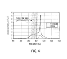
- FIG. 4 illustrates absorption spectra of the sensitizer ions and laser active ions
- FIG. 5 illustrates matching between emission and absorption spectra of the laser active ions
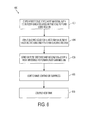
- FIG. 6 illustrates a flowchart for a method of making a laser gain medium, in accordance with an aspect of the disclosure.
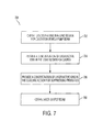
- FIG. 7 illustrates a flowchart of a method for suppressing parasitics in a laser device, in accordance with an aspect of the disclosure.
- Optical system 100 includes pump source 102 coupled optically to an optical device 106.
- Pump source 102 comprises a laser source (not shown) outputting pump beam 104 at a first wavelength.
- the first wavelength can be in a range of 920-960 nm
- the laser source used in pump source 102 can be a semiconductor laser operating in this range of wavelength. Since lasers used for pump sources are known to those of ordinary skill in the art, such laser devices that can be used for pump source 102 will not be described in detail herein.
- pump source 102 includes other electronic and optical components known to those of ordinary skill in the art.
- Pump source 102 can include pump diode arrays, for example, a 940nm 3-halfbar stack (5 mm wide) provided by Lasertel of Arlington, Arizona, although pump sources provided by other vendors may be used. In one exemplary arrangement, pump source 102 can be used in an end-pumping or side-pumping arrangement to reduce sensitivity of optical system 100 to pump wavelength. It is to be noted that although in the block diagram of optical system 100, pump source 102 is shown outside optical device 106, in alternative aspects of the disclosure, pump source 102 may be integrated with, and/or be inside optical device 106.
- pump beam 104 is provided to optical device 106 incident at first cladding region 108a of optical device 106, although pump beam 104 may be incident upon other components of optical device 106, for example, collimating optics, beam splitters, focusing lenses, and the like. In an alternative aspect of the disclosure, pump beam 104 may be incident upon second cladding region 108b. As noted above, pump beam 104 can be in a wavelength range 920-960 nm, although other suitable wavelengths and/or wavelength ranges may be used.
- pump beam 104 is substantially at 940 nm, when accounted for a linewidth and other drift parameters inherently associated with a wavelength of pump beam 104 (e.g., the first wavelength), although other suitable optical wavelengths may be used (e.g. , any wavelength in the range 920-960 nm).
- pump beam 104 is at a wavelength suitable to pump sensitizer ions present in core region 110 of optical device 106, such that cladding regions 108a and 108b are substantially lossless or transparent to passage of pump beam 104.
- laser active ions present in cladding regions 108a and 108b do not absorb pump beam 104 from pump source 102.
- Pump beam 104 passes through at least one of cladding regions 108a and 108b, depending upon an arrangement of pump source 102 relative to optical device 106, to excite or pump sensitizer ions present in core region 110.
- core region 110 and cladding regions 108a and 108b form a monolithic slab in which core region 110 forms a laser gain medium.
- optical device 106 is a laser device that outputs a laser beam at a second wavelength, different from the first wavelength of pump beam 104.
- optical device 106 can include components not explicitly shown in FIG. 1 .
- optical device 106 can include E-wave coatings on cladding regions 108a and 108b for coupling one or more heat sink devices to optical device 106, for dissipating heat.
- optical device 106 can comprise optical, electronic, mechanical, opto-mechanical, and/or electro-mechanical components for various functions such as focusing pump beam 104, impedance matching devices, aligning components, and the like.
- such components can include shutters, lenses, beam splitters, optical and electronic filters, couplers, optical fibers, windows, static and movable mirrors, prisms, optical coatings, glass slabs, thin films, light emitting diodes (LEDs), piezoelectric or other motion control devices, collimators, pins, bayonets, photoelectric cells, slides, cover slips, retardation plates, wave-plates, counters, and/or other additional components useful in assembly and function of optical system 100.
- shutters lenses, beam splitters, optical and electronic filters, couplers, optical fibers, windows, static and movable mirrors, prisms, optical coatings, glass slabs, thin films, light emitting diodes (LEDs), piezoelectric or other motion control devices, collimators, pins, bayonets, photo
- optical device 106 When used as a part of optical system 100, optical device 106 can be further coupled to a processor and a memory device (not shown) for carrying out analysis of output of optical device 106.
- a processor can be a part of a computing device and can be configured to execute instructions residing upon the memory device.
- optical device 106 is coupled to an oscilloscope or other form of display to aid a technician in carrying out analysis of various parameters associated with optical system 100, as can be contemplated by one of ordinary skill in the art in view of this disclosure.
- optical device 106 and/or pump source 102 can be operating on an optical table, bench, or rail (not shown) made of steel with a thick honeycomb lattice structure for supporting various components of optical system 100.
- At least one of cladding regions 108a and 108b is arranged to receive pump beam 104.
- Cladding regions 108a and 108b are doped with a concentration of ions that do not absorb pump beam 104.
- Cladding regions 108a and 108b at least partially surround core region 110.
- cladding regions 108a and 108b can completely surround core region 110, for example, as in a cylindrical geometry of an optical fiber. In such an arrangement, only one cladding region exists since cladding regions 108a and 108b are merged into a single cladding region with an annular ring type cross-sectional area.
- cladding regions 108a and 108b are doped with a concentration of laser active ions that absorb at least a portion of lasing wavelength from core region 110 of optical device 106 that enters cladding regions 108a and 108b, as discussed in detail below with respect to FIG. 2 .
- core region 110 may be doped with a concentration of laser active ions similar to the laser active ions in cladding regions 108a and 108b, and additionally, with a concentration of another type of ions, referred to as sensitizer ions herein, for absorbing pump beam 104 for excitation.
- Excitation of sensitizer ions in core region 110 causes the laser active ions to lase, resulting in an output beam 112 at a wavelength different from the wavelength of pump beam 104.
- This wavelength is also referred to herein as the lasing wavelength.
- core region 110 can have gain in a transverse direction which can cause losses due to parasitics when the lasing wavelength enters cladding regions 108a and 108b.
- the concentration of laser active ions in cladding regions 108a and 108b is at a level controlled to absorb the light or radiation (and therefore, energy) along a transverse direction thereby resulting in suppression of parasitics in optical device 106.
- cladding regions 108a and/or 108b are devoid of any sensitizer ions.
- Output beam 112 can be used for additional pumping or other laser applications, as can be contemplated by one of ordinary skill in the art.
- output beam 112 has a wavelength substantially equal to 1534 nm when accounted for linewidth and other drift parameters inherently associated with generation of a laser wavelength, although other wavelengths may be used, At this wavelength, output beam 112 is safe to the human eye.
- cladding regions 108a and 108b and core region 110 are illustrated. It is to be noted that, although particular dimensions and a rectangular cross-section geometry of cladding regions 108a and 108b and core region 110 are illustrated in FIG. 2 , one of ordinary skill in the art in view of this disclosure may contemplate other dimensions and geometries in which cladding regions 108a and 108b and core region 110 are structured and arranged.
- cladding regions 108a and 108b and core region 110 may be in the form of a preform that can be pulled at a controlled rate to form at least a portion of a fiber laser device in a cylindrical geometry with a circular cross-section.
- cladding regions 108a and 108b and core region 110 can be in the shape of slabs, as shown in FIG. 2 , of different dimensions.
- cladding regions 108a and 108b and core region 110 are each 1mm x 1mm x 10mm in height, breadth, and length, respectively.
- the structure formed by core region 110 and cladding regions 108a and 108b can be pumped by pump beam 104 through one of the 1mm x 3mm surfaces, with the 3mm surface aligned with a slow axis of a pump diode array in pump source 102.
- optical device 106 provides a larger pump aperture for pump beam 104, as compared to providing pump beam 104 to core region 110 only.
- a cross-section area of core region 110 is 1 mm 2 but a combined cross section area of core region 110 and cladding regions 108a and 108b is 3 mm 2 .
- pump beam 104 can be incident from any other direction (e.g. , sideways instead of from the top).
- output beam 112 can be emitted in other directions that are controllable by a designer of optical system 100.
- Cladding regions 108a and 108b and core region 110 form a monolithic laser gain medium.
- Cladding regions 108a and 108b can be made of phosphate glass or silicate glass host material, for example, Kigre QX/Er ® phosphate glass host material or Kigre MM-2 ® glass host material provided by Kigre, Inc. of Hilton Head, South Carolina.
- Kigre QX/Er ® phosphate glass host material or Kigre MM-2 ® glass host material provided by Kigre, Inc. of Hilton Head, South Carolina.
- glass host material Schott LG-910 ® provided by Schott of Mainz, Germany could be used.
- Other solid state host materials such as those provided by NP Photonics of Arlington, Arizona, or other glass from other manufacturers may be used.
- core region 110 can be made of phosphate glass or silicate glass host material thermally matched with the glass material used for cladding regions 108a and 108b, for example those provided by the above-noted manufacturers or other vendors.
- core region 110 includes one group of sensitizer ions at a first doping concentration that can be excited from a ground state to an excited state by pump beam 104.
- core region 110 also includes a second group of laser active ions at a second concentration that get excited from a ground state to an excited state by energy transfer from the sensitizer ions when the sensitizer ions return to the ground state. The process of energy transfer from sensitizer ions to laser active ions in core region 110 is described in detail with respect to FIG. 3 .
- cladding regions 108a and 108b are doped with a concentration of laser active ions only, with no sensitizer ions being present in cladding regions 108a and 108b. Since laser active ions are transparent to pump beam 104, pump beam 104 can travel without any loss through cladding regions 108a and/or 108b before reaching gain medium in core region 110. At the same time, doping cladding regions 108a and 108b with laser active ions facilitates suppression of parasitics resulting from a portion of lasing output beam 112 that enters cladding regions 108a and 108b, as discussed below.
- core region 110 comprises trivalent Erbium ions (Er 3+ ) from Er 2 O 3 as the laser active ions and trivalent Ytterbium ions (Yb 3+ ) from Yb 2 O 3 as the sensitizer ions that absorb energy from pump beam 104, although other types of laser active ions such as Holmium (Ho) ions and sensitizer ions such as Thulium TM ions may be used.
- laser active Er 3+ ions present in core region 110 may have a doping concentration of about 1.5% by weight.
- Sensitizer ions Yb 3+ present in core region 110 may have a doping concentration of about 18% by weight.
- core region 110 other doping concentrations and ranges for core region 110 could be used, for example, Er 3+ ions could be present in a range of 0.5-3% - and Yb 3+ ions can be present in a range of 6-18% by weight.
- Cladding regions 108a and 108b comprise only laser active ions Er 3+ from Er 2 O 3 with a doping concentration of 1.5% by weight Er 3+ ions.
- other doping concentrations and ranges for cladding regions 108a and 108b could be used, for example, Er 3+ ions could be present in a range of 0.5-3% in cladding regions 108a and 108b.
- doping concentrations of the ions in core region 110 and cladding regions 108a and 108b can be controlled and modified such that core region 110 and cladding regions 108a and 108b have matching coefficients of thermal expansion (CTE).
- core region 110 and cladding regions 108a and 108b may have additional matching characteristics such as thermal conductivity or refractive index.
- pump beam 104 is confined to wavelengths that are absorbed only by the sensitizer ions (e.g., Yb 3+ ions) such that the laser-active ions (e.g., Er 3+ ions) will be excited in core region 110 by absorbing energy from excited Yb 3+ ions, but not in cladding regions 108a and/or 108b.
- the laser-active ions in cladding regions 108a and/or 108b will remain unexcited and therefore, will absorb fluorescence generated in core region 110, thereby suppressing parasitics in the laser gain medium of optical device 106.
- laser-active-ion-doping in cladding regions 108a and/or 108b advantageously supports same host material (e.g. , phosphate, silicate, or the like) for both core region 110 and cladding regions 108a and 108b making the arrangement shown in FIG. 2 ideal for CTE matching.
- host material e.g. , phosphate, silicate, or the like
- laser active ions, and not sensitizer ions are present in cladding regions 108a and 108b, transmission of pump beam 104 can be carried out without loss while at the same time be useful in parasitic suppression in the co-doped gain medium forming core region 110.
- parasitics in the co-doped laser gain medium formed in core region 110 are suppressed since the pump bands of the two ion species (laser active and sensitizer ions) do not completely overlap.
- the sensitizer ions can be a two-level system
- the laser active ions can be a three-level or a quasi-three-level energy system, as discussed below with respect to FIG. 3-5 .
- the 3 x 10 mm surface(s) of glass slab including core region 110 and cladding regions 108a and 108b can have different configurations.
- an E-wave coating would be applied to one or both of the 3 x 10 mm surfaces and the slab for "dry" mounting (soldered or with a non-adhesive thermo-optical interface material).
- a thin layer of optical adhesive such as EPO-TEK OG134 ® provided by Epoxy Technology, Inc. of Billerica, Massachusetts
- the resonator mirror coating would be applied to the 1 x 3 mm surface through which pump beam 104 enters.
- an E-wave coating provides a protective layer on the monolithic slab that allows the wavelength corresponding to pump beam 104 to be substantially 100% reflective (e.g. , 99.9% reflective) at the second wavelength (lasing wavelength corresponding to output beam 112) as a result of total internal reflection at a boundary between the E-wave coating (or optical adhesive) and core region 110 and cladding regions 108a, and 108b on which the E-wave coating (or optical adhesive) is applied.
- the E-wave coating could be a 3-4 micron thick layer of SiO 2 as provided by TwinStar Optics, Coatings, and Crystals of New Port Richey, Florida.
- System 302 is a two-level Yb 3+ system and system 304 is a three-level or a quasi-three-level system.
- Er 3+ and Yb 3+ systems are illustrated in FIG. 3
- other equivalent and suitable two-level, three-level, quasi-three-level, and/or higher-level lasing systems may be used for different wavelengths of pump beam 104 and output beam 112.
- other two-level and three-level or quasi-three-level sources may include Ho, Tm ion systems.
- Yb 3+ ions in core region 110 in a ground state 306 transition to an excited energy level 308 by absorption of energy from pump beam 104.
- pump beam 104 is at a wavelength substantially equal to 940nm.
- excited Yb 3+ ions in core region 110 when returning back to ground state 306, transfer energy to Er 3+ ions in core region 110 that are in a ground state 312.
- the cross-relaxation process is symbolically shown by a chained curve 310. Since cross-relaxation energy processes generally are known, they will not be described in detail herein.
- Er 3+ ions in core region 110 transition to an excited state 314. Since Er 3+ ions form the three-level or the quasi-three-level system 304, excited Er 3+ ions in excited state 314 do not directly return to ground state 312. Instead, excited Er 3+ ions in excited state 314 return via a relatively fast process shown by an arrow 316 to an intermediate energy state 318, before finally returning to ground state 312, and emit photons lasing at the second wavelength (in this example, at about 1534nm). It is these lasing photons that form output beam 112 emanating from core region 110.
- cladding regions 108a and 108b do not have any sensitizer ions that can absorb pump beam 104 (e.g., no Yb 3+ ions), but only have laser active ions ( e.g., Er 3+ ions), pump beam 104 passes through cladding regions 108a and 108b without any significant loss in energy.
- FIG. 4 shows absorption spectra of Er 3+ and Yb 3+ ions at different wavelengths.
- Er 3+ ions present in cladding regions 108a and 108b show no absorption of electromagnetic energy in 920-960nm range, which is advantageous in many applications where temperature control of pump diodes in pump source 102 is difficult.
- the laser active ions (Er 3+ ions) in core region 110 show similar characteristics and do not absorb energy from pump beam 104.
- the absorption spectra shown in FIG. 3 also shows Yb 3+ ions present in core region 110 being capable of absorbing energy at pump wavelengths in the range 920-960nm from pump beam 104.
- Er 3+ ions present in cladding regions 108a and 108b can absorb any portion of energy from the lasing photons in core region 110 by absorbing the light that propagates along a transverse direction to excite Er 3+ ions in cladding regions 108a and 108b to intermediate energy state 318, as shown by an arrow 320.
- This is better understood from substantially matching emission and absorption spectra of Er 3+ ions shown in FIG. 5 .
- FIG. 5 illustrates Er 3+ ions to be capable of absorbing wavelength at or about 1534nm, as shown in the absorption peak, which matches the emission peak of Er 3+ ions in core region 110 that emit output beam 112.
- various aspects of this disclosure suppress parasitics in a laser gain medium forming core region 110 by absorbing energy of at least a transverse portion of output beam 112 at a lasing wavelength (e.g. , 1534nm), after sensitizer ions have been pumped at a pump wavelength by pump beam 104 for transferring energy to the laser active ions in core region 110 such that the parasitic transverse portion does not gain energy indefinitely by passing through core region 110 again and again.
- a lasing wavelength e.g. 1534nm
- the monolithic slab arrangement shown in FIG. 2 advantageously facilitates mounting and alignment of optical device 106, and provides better cooling characteristics since optical device 106 can dissipate heat via heat-sink on surface area larger than that of a device using only core region 110 as a gain medium with no cladding. Additionally, a wide slow-axis aperture of the co-doped slab accommodates lower-brightness diodes resulting in lower pump energies and flexible resonator design. Furthermore, laser-active-ion-doped side cladding eliminates the need for parasitic side treatments, thereby reducing costs.
- Flowchart 600 begins at procedure 602 where doping a first solid state host material with sensitizer ions (e.g., Yb 3+ ions) and laser active ions (e.g., Er 3+ ions) is carried out.
- the co-doped solid state host material forms the laser gain medium of core region 110 of optical device 106, and can be, by way of example only, a phosphate or a silicate host material.
- the solid state host material is described as "co-doped" since two different types of ion species, sensitizer and laser active, are doped in the same host material.
- the sensitizer ions absorb energy at a first wavelength that is a pump wavelength to transition to an excited state (e.g. , excited state 308 of FIG. 3 ).
- the laser active ions receive energy transferred from the sensitizer ions, when the sensitizer ions return to the unexcited state ( e.g. , ground state 306).
- the laser active ions Upon receiving the energy through cross-relaxation or other energy transfer processes, the laser active ions transition to an excited state (e.g. , excited state 314) only to return back to ground state 312 via intermediate state 318.
- laser active ions emit lasing photons at a lasing wavelength (e.g. , 1534nm) to form output beam 112.
- the flow of flowchart 600 then proceeds to procedure 604 where doping a second solid state host material with the laser active ions to form cladding regions 108a and/or 108b.
- the second solid state host material can be, by way of example only, a phosphate or a silicate host material.
- the laser active ions in cladding regions 108a and/or 108b are capable of suppressing parasitics in the laser gain medium of optical device 106 by absorbing energy of at least a transverse portion of the wavelength of lasing photons of output beam 112 from core region 110 in procedure 602, that enters cladding regions 108a and/or 108b.
- doping concentration of laser active ions in the first solid state host material forming core region 110 is equal to the doping concentration of the laser active ions in the second solid state host material forming the cladding regions 108a and 108b.
- unbonded cladding regions 108a and/or 108b and core region 110 may form a preform for pulling into a fiber at a controlled rate. Cladding regions 108a and 108b can partially or fully surround core region 110.
- the flow proceeds to procedure 608 where coating at least one surface of the first and second solid state host materials with an E-wave coating that thermally couples a heat sink device to cladding regions 108a and/or 108b is carried out.
- the E-wave coating is about 100% reflective at the first wavelength as a result of total internal reflection at the boundary between the E-wave coating and cladding regions 108a and 108b. Since various E-wave coatings have been described above, such description is not repeated here.
- procedure 610 coupling the heat sink to cladding regions 108a and/or 108b is carried out.
- optical device 106 may be used for generating lasing output beam 112 by exposure of the E-wave coating to pump beam 104 ( e.g. , at 940nm).
- procedure 610 can additionally include performing alignment of optical components, balancing impedance and other optimization procedures for optical device 106.
- Flowchart 700 begins at procedure 702 where exposing a concentration of sensitizer ions in core region 110 of the laser device to electromagnetic radiation at a first wavelength is carried out using pump beam 104. The exposing excites the sensitizer ions from ground state 306 to excited state 308. At procedure 704, providing a first concentration of laser active ions in core region 110 at ground state 312 is carried out.
- the laser active ions are excited to excited state 314 by receiving energy from the excited sensitizer ions when the excited sensitizer ions return to ground state 306 from excited state 308, the laser active ions lasing at a second wavelength when returning to ground state 312 from excited state 314 after the receiving is carried out.
- providing a second concentration of laser active ions in cladding regions 108a and/or 108b at least partially surrounding core region 110 is carried out.
- the second concentration of laser active ions suppress parasitics by absorbing energy in at least a portion of the second wavelength entering cladding regions 108a and/or 108b.
- cladding regions 108a and/or 108b are devoid of sensitizer ions, and comprise laser active ions only.
- output beam 112 lasing at the second wavelength e.g. , 1534nm
- flowcharts 600 and 700 shown in FIGS. 6 and 7 are representative of, for example, a method of making optical device 106 and laser gain medium therein, and for suppressing parasitics in a laser device ( e.g. , optical device 106), as shown in FIGS. 1-2 .
- Various operations or procedures shown in flowcharts 600 and 700 can be facilitated by one or more processors and peripheral devices on which machine readable instructions reside, for example, in a memory device coupled to the one or more processors.
- some portions of the procedures represented by the methods of flowcharts 600 and 700 of FIGS. 6 and 7 may be implemented manually at an optical bench, or may be carried out in a process controlled environment (e.g.
Landscapes
- Physics & Mathematics (AREA)
- Electromagnetism (AREA)
- Engineering & Computer Science (AREA)
- Plasma & Fusion (AREA)
- Optics & Photonics (AREA)
- Chemical & Material Sciences (AREA)
- Crystallography & Structural Chemistry (AREA)
- Lasers (AREA)
Abstract
Description
- The present disclosure relates to generally to an optical device, and particularly to systems and methods for suppressing parasitics in a co-doped gain medium.
- Generally, parasitics in an optical device (e.g., a laser device) refer to phenomena that act to clamp or limit useful gain (e.g., longitudinal gain) within a gain medium of the optical device, for example, due to internal reflections. In many cases, parasitic optical rays undergo total internal reflection (TIR) within the gain medium and continuously loop around and increase in power (robbing useful gain) with virtually no loss. In one conventional approach, parasitic suppression is accomplished by using an E-wave coating directly on the gain medium that limits the numerical aperture (NA) of the gain medium. The E-wave coating must then be processed in some way on its outer surface to prevent parasitic rays from returning back into the gain medium (e.g., roughening the outer surface of the coating). These processes add cost and complexity to the overall design. Roughening the gain medium surface alone (without an E-wave coating) has been tried, but this greatly increases the scattering loss of the guided pump light, which is highly undesirable as it reduces pump energy. Another conventional approach involves use of an optical adhesive with a refractive index sufficient to limit the gain medium NA. Typically, the adhesive is used to secure the gain medium to a heat-sink and therefore, is applied on the cooling surfaces of the gain medium. It is not convenient to use this adhesive on surfaces not involved in cooling or mounting. Another issue with optical adhesives is their high coefficient of thermal expansion (CTE). This property can significantly reduce the alignment stability of the gain medium over ranges of environmental temperature and pump power.
- Another conventional device includes a bonded absorbing side cladding that undesirably absorbs pump energy. Yet another conventional arrangement includes doped glass slides between gain elements, but again suffers from the cost and CTE mismatch drawbacks, in addition to increasing processing steps and complexity of the overall optical system. Still yet another conventional arrangement includes providing sensitizer ions in cladding region surrounding the gain medium for absorbing lasing wavelength entering the cladding, to suppress amplified spontaneous emission and parasitic lasing in a plane transverse to the lasing direction. However, this conventional approach still suffers from drawbacks as a substantial portion of the lasing wavelength entering the cladding region is not absorbed due to mismatches in the absorption spectrum of sensitizer ions and the emission spectrum of laser active ions in the gain medium, which are the source of the lasing wavelength, thereby causing parasitics to still exist substantially.
- According to one aspect of the present disclosure, an optical device is provided. The optical device includes a core region comprising a plurality of a first type of ions that absorb energy at a first wavelength and transfer the absorbed energy to a plurality of a second type of ions that lase at a second wavelength after receiving the transferred energy. The optical device includes a cladding region coupled to the core region comprising another plurality of the second type of ions that suppress parasitics in the optical device by absorbing energy of at least a transverse portion of the second wavelength that enters the cladding region.
- According to another aspect of the present disclosure, a method of making a laser gain medium is provided. The method includes doping a first solid state host material with sensitizer ions that absorb energy at a first wavelength and laser active ions that lase at a second wavelength after receiving energy transferred from the sensitizer ions to form a core region, and doping a second solid state host material with the laser active ions to form a cladding region, the laser active ions suppressing parasitics in the laser gain medium by absorbing energy of at least a transverse portion of the second wavelength that enters the cladding region. The method includes bonding the first and the second solid state host materials to form the laser gain medium.
- According to yet another aspect of the present disclosure, method for suppressing parasitics in a laser device is provided. The method includes exposing a concentration of sensitizer ions in a core region of the laser device to electromagnetic radiation at a first wavelength to excite the sensitizer ions from a first ground state to a first excited state. The method includes providing a first concentration of laser active ions in the core region at a second ground state, wherein the laser active ions are being excited to a second excited state by receiving energy from the excited sensitizer ions when the excited sensitizer ions return to the first ground state from the first excited state, the laser active ions lasing at a second wavelength when returning to the second ground state from the second excited state after the receiving. The method includes providing a second concentration of laser active ions in a cladding region at least partially surrounding the core region, the second concentration of laser active ions suppressing parasitics by absorbing energy in at least a portion of the second wavelength entering the cladding region.
- Other features of one or more aspects of the present disclosure will become apparent from the following detailed description, accompanying drawings, and the appended claims.
- Various aspects of the disclosure will now be disclosed, by way of example only, with reference to the accompanying schematic drawings and flowcharts in which corresponding reference symbols indicate corresponding parts, in which:
-
FIG. 1 illustrates a partly functional and partly schematic block diagram of an optical system, in accordance with an aspect of the present disclosure; -
FIG. 2 illustrates an exemplary arrangement and structure of cladding regions and core region in an optical device, in accordance with an aspect of the disclosure; -
FIG. 3 illustrates a two level energy system of sensitizer ions and a three level or quasi-three-level energy system of laser active ions; -
FIG. 4 illustrates absorption spectra of the sensitizer ions and laser active ions; -
FIG. 5 illustrates matching between emission and absorption spectra of the laser active ions; -
FIG. 6 illustrates a flowchart for a method of making a laser gain medium, in accordance with an aspect of the disclosure; and -
FIG. 7 illustrates a flowchart of a method for suppressing parasitics in a laser device, in accordance with an aspect of the disclosure. - Referring to
FIG. 1 ,optical system 100 in accordance with an aspect of this disclosure is illustrated.Optical system 100 includespump source 102 coupled optically to anoptical device 106.Pump source 102 comprises a laser source (not shown) outputtingpump beam 104 at a first wavelength. By way of example only and not by way of limitation, the first wavelength can be in a range of 920-960 nm, and the laser source used inpump source 102 can be a semiconductor laser operating in this range of wavelength. Since lasers used for pump sources are known to those of ordinary skill in the art, such laser devices that can be used forpump source 102 will not be described in detail herein. In addition,pump source 102 includes other electronic and optical components known to those of ordinary skill in the art.Pump source 102 can include pump diode arrays, for example, a 940nm 3-halfbar stack (5 mm wide) provided by Lasertel of Tucson, Arizona, although pump sources provided by other vendors may be used. In one exemplary arrangement,pump source 102 can be used in an end-pumping or side-pumping arrangement to reduce sensitivity ofoptical system 100 to pump wavelength. It is to be noted that although in the block diagram ofoptical system 100,pump source 102 is shown outsideoptical device 106, in alternative aspects of the disclosure,pump source 102 may be integrated with, and/or be insideoptical device 106. - In one aspect of the disclosure,
pump beam 104 is provided tooptical device 106 incident atfirst cladding region 108a ofoptical device 106, althoughpump beam 104 may be incident upon other components ofoptical device 106, for example, collimating optics, beam splitters, focusing lenses, and the like. In an alternative aspect of the disclosure,pump beam 104 may be incident upon secondcladding region 108b. As noted above,pump beam 104 can be in a wavelength range 920-960 nm, although other suitable wavelengths and/or wavelength ranges may be used. For example, in one aspect of the disclosure,pump beam 104 is substantially at 940 nm, when accounted for a linewidth and other drift parameters inherently associated with a wavelength of pump beam 104 (e.g., the first wavelength), although other suitable optical wavelengths may be used (e.g., any wavelength in the range 920-960 nm). In one aspect of the disclosure,pump beam 104 is at a wavelength suitable to pump sensitizer ions present incore region 110 ofoptical device 106, such thatcladding regions pump beam 104. In other words, laser active ions present incladding regions pump beam 104 frompump source 102.Pump beam 104 passes through at least one ofcladding regions pump source 102 relative tooptical device 106, to excite or pump sensitizer ions present incore region 110. - In one aspect of the disclosure,
core region 110 andcladding regions core region 110 forms a laser gain medium. In another aspect of the disclosure,optical device 106 is a laser device that outputs a laser beam at a second wavelength, different from the first wavelength ofpump beam 104. In addition,optical device 106 can include components not explicitly shown inFIG. 1 . For example,optical device 106 can include E-wave coatings oncladding regions optical device 106, for dissipating heat. Further,optical device 106 can comprise optical, electronic, mechanical, opto-mechanical, and/or electro-mechanical components for various functions such as focusingpump beam 104, impedance matching devices, aligning components, and the like. By way of example only and not by way of limitation, such components can include shutters, lenses, beam splitters, optical and electronic filters, couplers, optical fibers, windows, static and movable mirrors, prisms, optical coatings, glass slabs, thin films, light emitting diodes (LEDs), piezoelectric or other motion control devices, collimators, pins, bayonets, photoelectric cells, slides, cover slips, retardation plates, wave-plates, counters, and/or other additional components useful in assembly and function ofoptical system 100. When used as a part ofoptical system 100,optical device 106 can be further coupled to a processor and a memory device (not shown) for carrying out analysis of output ofoptical device 106. Such a processor can be a part of a computing device and can be configured to execute instructions residing upon the memory device. Further, in one aspect of the disclosure,optical device 106 is coupled to an oscilloscope or other form of display to aid a technician in carrying out analysis of various parameters associated withoptical system 100, as can be contemplated by one of ordinary skill in the art in view of this disclosure. In one aspect of the disclosure,optical device 106 and/or pumpsource 102 can be operating on an optical table, bench, or rail (not shown) made of steel with a thick honeycomb lattice structure for supporting various components ofoptical system 100. - At least one of
cladding regions pump beam 104.Cladding regions pump beam 104.Cladding regions core region 110. In one aspect of the disclosure,cladding regions core region 110, for example, as in a cylindrical geometry of an optical fiber. In such an arrangement, only one cladding region exists sincecladding regions cladding regions core region 110 ofoptical device 106 that enterscladding regions FIG. 2 . As also discussed in detail with respect toFIGS. 2-7 ,core region 110 may be doped with a concentration of laser active ions similar to the laser active ions incladding regions pump beam 104 for excitation. Excitation of sensitizer ions incore region 110 causes the laser active ions to lase, resulting in anoutput beam 112 at a wavelength different from the wavelength ofpump beam 104. This wavelength is also referred to herein as the lasing wavelength. In one embodiment of the disclosure,core region 110 can have gain in a transverse direction which can cause losses due to parasitics when the lasing wavelength enterscladding regions cladding regions optical device 106. In an aspect of the disclosure,cladding regions 108a and/or 108b are devoid of any sensitizer ions.Output beam 112 can be used for additional pumping or other laser applications, as can be contemplated by one of ordinary skill in the art. In this example,output beam 112 has a wavelength substantially equal to 1534 nm when accounted for linewidth and other drift parameters inherently associated with generation of a laser wavelength, although other wavelengths may be used, At this wavelength,output beam 112 is safe to the human eye. - Referring to
FIG. 2 , an exemplary arrangement and structure ofcladding regions core region 110 is illustrated. It is to be noted that, although particular dimensions and a rectangular cross-section geometry ofcladding regions core region 110 are illustrated inFIG. 2 , one of ordinary skill in the art in view of this disclosure may contemplate other dimensions and geometries in whichcladding regions core region 110 are structured and arranged. For example,cladding regions core region 110 may be in the form of a preform that can be pulled at a controlled rate to form at least a portion of a fiber laser device in a cylindrical geometry with a circular cross-section. Similarly,cladding regions core region 110 can be in the shape of slabs, as shown inFIG. 2 , of different dimensions. In the example ofFIG. 2 ,cladding regions core region 110 are each 1mm x 1mm x 10mm in height, breadth, and length, respectively. The structure formed bycore region 110 andcladding regions pump beam 104 through one of the 1mm x 3mm surfaces, with the 3mm surface aligned with a slow axis of a pump diode array inpump source 102. The longer (3 mm) dimension in the slow axis reduces the brightness requirement for pump diodes inpump source 102 resulting in design flexibility ofoptical system 100. In one aspect of the disclosure, the slab is mounted and cooled on one or both of the large surfaces (3 x 10 mm). As a result of the exemplary arrangement shown inFIG. 2 ,optical device 106 provides a larger pump aperture forpump beam 104, as compared to providingpump beam 104 tocore region 110 only. For example, inFIG. 2 a cross-section area ofcore region 110 is 1 mm2 but a combined cross section area ofcore region 110 andcladding regions pump beam 104 incident onoptical device 106. It is to be noted that the direction of incidence ofpump beam 104 as shown inFIG. 2 is by way of example only and not by way of limitation, and one of ordinary skill in the art will appreciate thatpump beam 104 can be incident from any other direction (e.g., sideways instead of from the top). Similarly, based upon specific system design parameters of optical device 106 (e.g., placement of output lenses),output beam 112 can be emitted in other directions that are controllable by a designer ofoptical system 100. - In one aspect of the disclosure,
cladding regions core region 110 form a monolithic laser gain medium.Cladding regions core region 110 can be made of phosphate glass or silicate glass host material thermally matched with the glass material used forcladding regions core region 110 includes one group of sensitizer ions at a first doping concentration that can be excited from a ground state to an excited state bypump beam 104. In addition,core region 110 also includes a second group of laser active ions at a second concentration that get excited from a ground state to an excited state by energy transfer from the sensitizer ions when the sensitizer ions return to the ground state. The process of energy transfer from sensitizer ions to laser active ions incore region 110 is described in detail with respect toFIG. 3 . In an aspect of the disclosure,cladding regions cladding regions beam 104,pump beam 104 can travel without any loss throughcladding regions 108a and/or 108b before reaching gain medium incore region 110. At the same time,doping cladding regions lasing output beam 112 that enterscladding regions - By way of example only,
core region 110 comprises trivalent Erbium ions (Er3+) from Er2O3 as the laser active ions and trivalent Ytterbium ions (Yb3+) from Yb2O3 as the sensitizer ions that absorb energy frompump beam 104, although other types of laser active ions such as Holmium (Ho) ions and sensitizer ions such as Thulium ™ ions may be used. Further by way of example only, laser active Er3+ ions present incore region 110 may have a doping concentration of about 1.5% by weight. Sensitizer ions Yb3+ present incore region 110 may have a doping concentration of about 18% by weight. In alternative aspects of the disclosure, other doping concentrations and ranges forcore region 110 could be used, for example, Er3+ ions could be present in a range of 0.5-3%- and Yb3+ ions can be present in a range of 6-18% by weight.Cladding regions cladding regions cladding regions core region 110 andcladding regions core region 110 andcladding regions core region 110 andcladding regions pump beam 104 is confined to wavelengths that are absorbed only by the sensitizer ions (e.g., Yb3+ ions) such that the laser-active ions (e.g., Er3+ ions) will be excited incore region 110 by absorbing energy from excited Yb3+ ions, but not incladding regions 108a and/or 108b. The laser-active ions incladding regions 108a and/or 108b will remain unexcited and therefore, will absorb fluorescence generated incore region 110, thereby suppressing parasitics in the laser gain medium ofoptical device 106. Additionally, use of laser-active-ion-doping incladding regions 108a and/or 108b advantageously supports same host material (e.g., phosphate, silicate, or the like) for bothcore region 110 andcladding regions FIG. 2 ideal for CTE matching. Furthermore, since laser active ions, and not sensitizer ions, are present incladding regions pump beam 104 can be carried out without loss while at the same time be useful in parasitic suppression in the co-doped gain medium formingcore region 110. According to one aspect of the disclosure, parasitics in the co-doped laser gain medium formed incore region 110 are suppressed since the pump bands of the two ion species (laser active and sensitizer ions) do not completely overlap. For example, the sensitizer ions can be a two-level system, whereas the laser active ions can be a three-level or a quasi-three-level energy system, as discussed below with respect toFIG. 3-5 . - Although not shown in
FIG. 2 , the 3 x 10 mm surface(s) of glass slab includingcore region 110 andcladding regions pump beam 104 enters. For example, an E-wave coating, or alternatively an optical adhesive, provides a protective layer on the monolithic slab that allows the wavelength corresponding to pumpbeam 104 to be substantially 100% reflective (e.g., 99.9% reflective) at the second wavelength (lasing wavelength corresponding to output beam 112) as a result of total internal reflection at a boundary between the E-wave coating (or optical adhesive) andcore region 110 andcladding regions - Referring to
FIG. 3 , a simplified Er3+, Yb3+ energy level system is illustrated.System 302 is a two-level Yb3+ system andsystem 304 is a three-level or a quasi-three-level system. It is to be noted although Er3+ and Yb3+ systems are illustrated inFIG. 3 , other equivalent and suitable two-level, three-level, quasi-three-level, and/or higher-level lasing systems may be used for different wavelengths ofpump beam 104 andoutput beam 112. For example, other two-level and three-level or quasi-three-level sources may include Ho, Tm ion systems. Whenpump beam 104 is incident onsystem 302, Yb3+ ions incore region 110 in aground state 306 transition to anexcited energy level 308 by absorption of energy frompump beam 104. In this example,pump beam 104 is at a wavelength substantially equal to 940nm. By a cross-relaxation process, excited Yb3+ ions incore region 110, when returning back toground state 306, transfer energy to Er3+ ions incore region 110 that are in aground state 312. The cross-relaxation process is symbolically shown by a chainedcurve 310. Since cross-relaxation energy processes generally are known, they will not be described in detail herein. Upon receiving energy from the Yb3+ ions returning toground state 306, Er3+ ions incore region 110 transition to anexcited state 314. Since Er3+ ions form the three-level or the quasi-three-level system 304, excited Er3+ ions inexcited state 314 do not directly return toground state 312. Instead, excited Er3+ ions inexcited state 314 return via a relatively fast process shown by anarrow 316 to anintermediate energy state 318, before finally returning toground state 312, and emit photons lasing at the second wavelength (in this example, at about 1534nm). It is these lasing photons that formoutput beam 112 emanating fromcore region 110. Sincecladding regions pump beam 104 passes throughcladding regions FIG. 4 that shows absorption spectra of Er3+ and Yb3+ ions at different wavelengths. For example, Er3+ ions present incladding regions pump source 102 is difficult. The laser active ions (Er3+ ions) incore region 110 show similar characteristics and do not absorb energy frompump beam 104. The absorption spectra shown inFIG. 3 also shows Yb3+ ions present incore region 110 being capable of absorbing energy at pump wavelengths in the range 920-960nm frompump beam 104. - However, referring back to
FIG. 3 , Er3+ ions present incladding regions core region 110 by absorbing the light that propagates along a transverse direction to excite Er3+ ions incladding regions intermediate energy state 318, as shown by anarrow 320. This is better understood from substantially matching emission and absorption spectra of Er3+ ions shown inFIG. 5 . For example,FIG. 5 illustrates Er3+ ions to be capable of absorbing wavelength at or about 1534nm, as shown in the absorption peak, which matches the emission peak of Er3+ ions incore region 110 that emitoutput beam 112. As a result of such absorption, parasitic light that enterscladding regions optical device 106. Absent the doping ofcladding regions cladding regions output beam 112 and transferring it to parasitic transverse portion that enterscladding regions cladding regions 108a and/or 108b with laser active ions andcore region 110 with both laser active and sensitizer ions, various aspects of this disclosure suppress parasitics in a laser gain medium formingcore region 110 by absorbing energy of at least a transverse portion ofoutput beam 112 at a lasing wavelength (e.g., 1534nm), after sensitizer ions have been pumped at a pump wavelength bypump beam 104 for transferring energy to the laser active ions incore region 110 such that the parasitic transverse portion does not gain energy indefinitely by passing throughcore region 110 again and again. - Further, the monolithic slab arrangement shown in
FIG. 2 advantageously facilitates mounting and alignment ofoptical device 106, and provides better cooling characteristics sinceoptical device 106 can dissipate heat via heat-sink on surface area larger than that of a device usingonly core region 110 as a gain medium with no cladding. Additionally, a wide slow-axis aperture of the co-doped slab accommodates lower-brightness diodes resulting in lower pump energies and flexible resonator design. Furthermore, laser-active-ion-doped side cladding eliminates the need for parasitic side treatments, thereby reducing costs. - Referring to
FIG. 6 , a method of making a laser gain medium is illustrated usingflowchart 600, in accordance with an aspect of the disclosure, with reference toFIGS. 1-5 .Flowchart 600 begins atprocedure 602 where doping a first solid state host material with sensitizer ions (e.g., Yb3+ ions) and laser active ions (e.g., Er3+ ions) is carried out. The co-doped solid state host material forms the laser gain medium ofcore region 110 ofoptical device 106, and can be, by way of example only, a phosphate or a silicate host material. The solid state host material is described as "co-doped" since two different types of ion species, sensitizer and laser active, are doped in the same host material. The sensitizer ions absorb energy at a first wavelength that is a pump wavelength to transition to an excited state (e.g.,excited state 308 ofFIG. 3 ). The laser active ions receive energy transferred from the sensitizer ions, when the sensitizer ions return to the unexcited state (e.g., ground state 306). Upon receiving the energy through cross-relaxation or other energy transfer processes, the laser active ions transition to an excited state (e.g., excited state 314) only to return back toground state 312 viaintermediate state 318. When returning from intermediate state, laser active ions emit lasing photons at a lasing wavelength (e.g., 1534nm) to formoutput beam 112. - The flow of
flowchart 600 then proceeds toprocedure 604 where doping a second solid state host material with the laser active ions to formcladding regions 108a and/or 108b. The second solid state host material can be, by way of example only, a phosphate or a silicate host material. The laser active ions incladding regions 108a and/or 108b are capable of suppressing parasitics in the laser gain medium ofoptical device 106 by absorbing energy of at least a transverse portion of the wavelength of lasing photons ofoutput beam 112 fromcore region 110 inprocedure 602, that enterscladding regions 108a and/or 108b. As noted above, the absorption of transverse portion ofoutput beam 112 generated incore region 110 occurs by the laser active ions incladding regions 108a and/or 108b transitioning in energy fromground state 312 to intermediateexcited state 318 and/orexcited state 314. In one aspect of the disclosure doping concentration of laser active ions in the first solid state host material formingcore region 110 is equal to the doping concentration of the laser active ions in the second solid state host material forming thecladding regions - The flow then proceeds to
procedure 606 where bonding the first and the second solid state host materials to form the laser gain medium ofoptical device 106. The bonding is carried out in a manner to ensure matching of CTEs and/or other characteristics (e.g., thermal conductivity or refractive index) of the first and the second host materials. In one aspect of the disclosure,unbonded cladding regions 108a and/or 108b andcore region 110 may form a preform for pulling into a fiber at a controlled rate.Cladding regions core region 110. - The flow proceeds to
procedure 608 where coating at least one surface of the first and second solid state host materials with an E-wave coating that thermally couples a heat sink device tocladding regions 108a and/or 108b is carried out. The E-wave coating is about 100% reflective at the first wavelength as a result of total internal reflection at the boundary between the E-wave coating andcladding regions - The flow then proceeds to
procedure 610 where coupling the heat sink tocladding regions 108a and/or 108b is carried out. Once coupled with the heat sink device,optical device 106 may be used for generatinglasing output beam 112 by exposure of the E-wave coating to pump beam 104 (e.g., at 940nm). In addition to coupling the heat sink device,procedure 610 can additionally include performing alignment of optical components, balancing impedance and other optimization procedures foroptical device 106. - Referring to
FIG. 7 , a method for suppressing parasitics in a laser device is illustrated usingflowchart 700, in accordance with an aspect of the disclosure, with reference back toFIGS. 1-5 .Flowchart 700 begins atprocedure 702 where exposing a concentration of sensitizer ions incore region 110 of the laser device to electromagnetic radiation at a first wavelength is carried out usingpump beam 104. The exposing excites the sensitizer ions fromground state 306 toexcited state 308. Atprocedure 704, providing a first concentration of laser active ions incore region 110 atground state 312 is carried out. The laser active ions are excited toexcited state 314 by receiving energy from the excited sensitizer ions when the excited sensitizer ions return toground state 306 fromexcited state 308, the laser active ions lasing at a second wavelength when returning toground state 312 fromexcited state 314 after the receiving is carried out. Atprocedure 706, providing a second concentration of laser active ions incladding regions 108a and/or 108b at least partially surroundingcore region 110 is carried out. The second concentration of laser active ions suppress parasitics by absorbing energy in at least a portion of the second wavelength enteringcladding regions 108a and/or 108b. In one aspect of the disclosure,cladding regions 108a and/or 108b are devoid of sensitizer ions, and comprise laser active ions only. Finally, atprocedure 708,output beam 112 lasing at the second wavelength (e.g., 1534nm) is obtained. - Generally,
flowcharts FIGS. 6 and7 are representative of, for example, a method of makingoptical device 106 and laser gain medium therein, and for suppressing parasitics in a laser device (e.g., optical device 106), as shown inFIGS. 1-2 . Various operations or procedures shown inflowcharts flowcharts FIGS. 6 and7 may be implemented manually at an optical bench, or may be carried out in a process controlled environment (e.g., a microfabrication laboratory) operated by a user. Further, although the example procedures of the methods are described with reference toflowcharts flowcharts core region 110 andcladding regions optical device 106. - While the present disclosure has been described in connection with specific aspects, it is to be understood that the inventive concept is capable of further modifications, and is not to be limited to the disclosed aspects, and this application is intended to cover any variations, uses, equivalent arrangements or adaptations of the present disclosure following, in general, the principles of the present disclosure and including such departures from the present disclosure as come within known or customary practice in the art to which the present disclosure pertains, and as may be applied to the essential hereinbefore set forth and followed in the spirit and scope of the appended claims.
- These and other aspects of the present disclosure, as well as the methods of operation and functions of the related elements of structure and the combination of parts and economies of manufacture, will become more apparent upon consideration of the following description and the appended claims with reference to the accompanying drawings, all of which form a part of this specification, wherein like reference numerals designate corresponding parts in the various figures. In one aspect of the disclosure, the structural components illustrated herein are drawn to scale. It is to be expressly understood, however, that the drawings are for the purpose of illustration and description only and are not a limitation. In addition, it should be appreciated that structural features shown or described in any one aspect herein can be used in other aspects as well. As used in the specification and in the claims, the singular form of "a", "an", and "the" include plural referents unless the context clearly dictates otherwise.
The present invention has the following aspects: - 1. An optical device, comprising:
- a core region comprising a plurality of a first type of ions that absorb energy at a first wavelength and transfer the absorbed energy to a plurality of a second type of ions that lase at a second wavelength after receiving the transferred energy; and
- a cladding region coupled to the core region comprising another plurality of the second type of ions that supress parasitics in the optical device by absorbing energy of at least a protion of the second wavelength that enters the cladding region.
- 2. The optical device of aspect 1, wherein the core region and the cladding region are arranged such that the cladding region at least partially surrounds the core region in a slab of rectangular or circular cross-sectional geometry.
- 3. The optical device of aspect 1 or
aspect 2, wherein the second type of ions are transparent to the first wavelength incident thereupon, the first wavelength providing pump energy to the first type of ions in the core region. - 4. The optical device of any one of aspects 1 to 3, wherein the first type of ions comprise a two level energy system and the second type of ions comprise a three level or a quasi-three level energy system.
- 5. The optical device of any one of aspects 1 to 4, wherein the first type of ions are trivalent Ytterbium ions (Yb3+) ions and the second type of ions are trivalent Erbium (Er3+) ions.
- 6. The optical device of
aspect 5, wherein the core region is a co-doped phosphate glass host material with a doping concentration of about 1.5% by weight Er3+ ions and about 18% by weight Yb3+ions, and the cladding region is an Erbium doped phosphate glass host material with a doping concentration of about 1.5% by weight Er3+ions. - 7. The optical device of any preceding aspect, wherein the core and the cladding regions are arranged to form a preform for an optical fiber pull.
- 8. The optical device of any preceding aspect, wherein the first wavelength is substantially equal to 940 nm and the second wavelength is substantially equal to 1534 nm.
- 9. The optical device of any preceding aspect, wherein the second type of ions have an emission spectrum matched to an absorption spectrum thereof for absorbing the energy of at least the transverse portion of the second wavelength that enters the cladding region.
- 10. The optical device of any preceding aspect, wherein the first type of ions transfer the energy to the second type of ions by a cross-relaxation energy transfer process.
- 11. The optical device of any preceding aspect, wherein the cladding region comprises an E-wave coating on at least one surface thereof that thermally couples a heat sink device to the cladding region, the E-wave coating being about 100% reflective at the first wavelength as a result of total internal reflection at the boundary between the E-wave coating and the cladding region.
- 12. A method of making a laser gain medium, comprising:
- doping a first solid state host material with sensitizer ions that absorb energy at a first wavelength and laser active ions that absorb energy at a second wavelength after receiving energy transferred from the sensitizer ions to form a core region;
- doping a second solid state host material with the laser active ions to form a cladding region, the laser active ions capable of supressing parasitics in the laser gain medium by absorbing energy of at least a transverse portion of the second wavelength that enters the cladding region; and
- bonding the first and second solid state host materials to form the laser gain medium.
- 13. The method of aspect 12, wherein the core region and the cladding region have matched Coefficients of Thermal Expansion (CTEs).
- 14. The method of aspect 12 or aspect 13, further comprising:
- coating at least one surface of the first and second solid state host materials with an E-wave coating for coupling a heat sink device to the cladding region, the E-wave coating being about 100% reflective at the first wavelength as a result of total internal reflection at the boundary between the E-wave coating and the cladding region; and
- exposing the E-wave coating to electromagnetic radiation from a pump source substantially outputting at the first wavelength, the laser active ions being substantially transparent to the first wavelength incident thereupon in the cladding region.
- 15. The method of any of aspects 12 to 14, wherein the sensitizer ions are trivalent Ytterbium ions (Yb3+)ions and the laser active ions are trivalent Erbium (Er3+) ions.
- 16. The method of any of aspects 12 to 15, wherein the first and second solid state host materials are both either a phosphate based or a silicate based material.
- 17. The method of any of aspects 12 to 16, wherein the bonding comprises:
- arranging the cladding region to at least partially surround the core region.
- 18. The method of any of aspects 12 to 17, further comprising:
- forming a preform with the core and the cladding regions; and
- pulling the preform at a controlled rate to form at least a portion of a fiber laser device.
- 19. The method of any of aspects 12 to 18, wherein the doping the first solid state host material comprises doping to a concentration of about 1.5% by weight Er3+ ions and about 18% by weight Yb3+ ions, and wherein the doping the second solid state host material comprises doping to a concentration of about 1.5% by weight Er3+ions.
- 20. A method for supressing parasites in a laser device, comprising:
- exposing a concentration of sensitizer ions in a core region of the laser device to electromagnetic radiation at a first wavelength to excite the sensitizer ions from a first ground state to a first excited state;
- providing a first concentration of laser active ions in the core region at a second ground state, wherein the laser active ions are excited to a second excited state by receiving energy from the excited sensitizer ions when the excited sensitizer ions return to the first ground state from the first excited state, the laser active ions lasing at a second wavelength when returning to the second ground state from the second excited state after the receiving; and
- providing a second concentration of laser active ions in a cladding region at least partially surrounding the core region, the second concentration of laser active ions supressing parasitics by absorbing energy in at least a portion of the second wavelength entering the cladding region.
- 21. The method of aspect 20, wherein the exposing comprises providing the electromagnetic radiation at the first wavelength form a laser pump source to the cladding region, the cladding region being transparent to the first wavelength.
- 22. The method of aspect 20 or aspect 21, wherein the first wavelength is substantially equal to 940 nm and the second wavelength is substantially equal to 1534 nm.
- 23. The method of any of aspects 20 to 22, wherein the sensitizer ions are trivalent Ytterbium ions (Yb3+) ions and the lase active ions are trivalent Erbium (Er3+) ions.
- 24. The method of aspect 23, wherein the core region is a co-doped phosphate glass host material with a doping concentration of about 1.5% by weight Er3+ ions and about 18% by weight Yb3+ions, and the cladding region is an Erbium doped phosphate glass host material with a doping concentration of about 1.5% by weight Er3+ions.
- 25. The method of any one of aspects 20 to 24, wherein the laser active ions have an emission spectrum matched to a absorption spectrum thereof.
- 26. The method of any one of aspects 20 to 25, wherein the laser active ions have at least one excited state in addition to and at a higher energy state than the second excited state, such that the laser active ions are excited to the additional excited state and return to the second excited state prior to the lasing by returning to the second ground state.
- 27. The method of any one of aspects 20 to 26, wherein the absorbing at least the portion of the second wavelength entering the cladding region occurs in a direction transverse relative to a direction of propagation of electromagnetic radiation at the second wavelength in the core region.
- 28. The method of any one of aspects 20 to 27, wherein the cladding region is devoid of the sensitizer ions.
- 29. The method of any one of aspects 20 to 28, wherein the first concentration is equal to the second concentration.
Claims (15)
- An optical device, comprising:a core region comprising a plurality of a first type of ions that absorb energy at a first wavelength and transfer the absorbed energy to a plurality of a second type of ions that lase at a second wavelength after receiving the transferred energy; anda cladding region coupled to the core region comprising another plurality of the second type of ions that supress parasitics in the optical device by absorbing energy of at least a protion of the second wavelength that enters the cladding region.
- The optical device of claim 1, wherein the core region and the cladding region are arranged such that the cladding region at least partially surrounds the core region in a slab of rectangular or circular cross-sectional geometry.
- The optical device of claim 1 or claim 2, wherein the second type of ions are transparent to the first wavelength incident thereupon, the first wavelength providing pump energy to the first type of ions in the core region.
- The optical device of any one of claims 1 to 3, wherein the first type of ions comprise a two level energy system and the second type of ions comprise a three level or a quasi-three level energy system.
- The optical device of any one of claims 1 to 4, wherein the first type of ions are trivalent Ytterbium ions (Yb3+) ions and the second type of ions are trivalent Erbium (Er3+) ions.
- The optical device of claim 5, wherein the core region is a co-doped phosphate glass host material with a doping concentration of about 1.5% by weight Er3+ ions and about 18% by weight Yb3+ions, and the cladding region is an Erbium doped phosphate glass host material with a doping concentration of about 1.5% by weight Er3+ions.
- The optical device of any one of claims 1 to 6, wherein the core and the cladding regions are arranged to form a preform for an optical fiber pull; and/or
wherein the first wavelength is substantially equal to 940 nm and the second wavelength is substantially equal to 1534 nm; and/or
wherein the second type of ions have an emission spectrum matched to an absorption spectrum thereof for absorbing the energy of at least the transverse portion of the second wavelength that enters the cladding region; and/or
wherein the first type of ions transfer the energy to the second type of ions by a cross-relaxation energy transfer process; and/or
wherein the cladding region comprises an E-wave coating on at least one surface thereof that thermally couples a heat sink device to the cladding region, the E-wave coating being about 100% reflective at the first wavelength as a result of total internal reflection at the boundary between the E-wave coating and the cladding region. - A method of making a laser gain medium, comprising:doping a first solid state host material with sensitizer ions that absorb energy at a first wavelength and laser active ions that absorb energy at a second wavelength after receiving energy transferred from the sensitizer ions to form a core region;doping a second solid state host material with the laser active ions to form a cladding region, the laser active ions capable of supressing parasitics in the laser gain medium by absorbing energy of at least a transverse portion of the second wavelength that enters the cladding region; andbonding the first and second solid state host materials to form the laser gain medium.
- The method of claim 8, wherein the core region and the cladding region have matched Coefficients of Thermal Expansion (CTEs).
- The method of claim 8 or claim 9, further comprising:coating at least one surface of the first and second solid state host materials with an E-wave coating for coupling a heat sink device to the cladding region, the E-wave coating being about 100% reflective at the first wavelength as a result of total internal reflection at the boundary between the E-wave coating and the cladding region; andexposing the E-wave coating to electromagnetic radiation from a pump source substantially outputting at the first wavelength, the laser active ions being substantially transparent to the first wavelength incident thereupon in the cladding region; and/orwherein the sensitizer ions are trivalent Ytterbium ions (Yb3+)ions and the laser active ions are trivalent Erbium (Er3+) ions; and/or
wherein the first and second solid state host materials are both either a phosphate based or a silicate based material; and/or
wherein the bonding comprises:
arranging the cladding region to at least partially surround the core region; and/or
further comprising:
forming a preform with the core and the cladding regions; and
pulling the preform at a controlled rate to form at least a portion of a fiber laser device;
and/or
wherein the doping the first solid state host material comprises doping to a concentration of about 1.5% by weight Er3+ ions and about 18% by weight Yb3+ ions, and wherein the doping the second solid state host material comprises doping to a concentration of about 1.5% by weight Er3+ ions. - A method for supressing parasites in a laser device, comprising:exposing a concentration of sensitizer ions in a core region of the laser device to electromagnetic radiation at a first wavelength to excite the sensitizer ions from a first ground state to a first excited state;providing a first concentration of laser active ions in the core region at a second ground state, wherein the laser active ions are excited to a second excited state by receiving energy from the excited sensitizer ions when the excited sensitizer ions return to the first ground state from the first excited state, the laser active ions lasing at a second wavelength when returning to the second ground state from the second excited state after the receiving; andproviding a second concentration of laser active ions in a cladding region at least partially surrounding the core region, the second concentration of laser active ions supressing parasitics by absorbing energy in at least a portion of the second wavelength entering the cladding region.
- The method of claim 11, wherein the exposing comprises providing the electromagnetic radiation at the first wavelength form a laser pump source to the cladding region, the cladding region being transparent to the first wavelength; and/or
wherein the first wavelength is substantially equal to 940 nm and the second wavelength is substantially equal to 1534 nm. - The method of claim 11 or claim 12, wherein the sensitizer ions are trivalent Ytterbium ions (Yb3+) ions and the lase active ions are trivalent Erbium (Er3+) ions.
- The method of claim 13, wherein the core region is a co-doped phosphate glass host material with a doping concentration of about 1.5% by weight Er3+ ions and about 18% by weight Yb3+ions, and the cladding region is an Erbium doped phosphate glass host material with a doping concentration of about 1.5% by weight Er3+ions.
- The method of any one of claims 11 to 14, wherein the laser active ions have an emission spectrum matched to a absorption spectrum thereof; and/or
wherein the laser active ions have at least one excited state in addition to and at a higher energy state than the second excited state, such that the laser active ions are excited to the additional excited state and return to the second excited state prior to the lasing by returning to the second ground state; and/or
wherein the absorbing at least the portion of the second wavelength entering the cladding region occurs in a direction transverse relative to a direction of propagation of electromagnetic radiation at the second wavelength in the core region; and/or
wherein the cladding region is devoid of the sensitizer ions; and/or
wherein the first concentration is equal to the second concentration.
Applications Claiming Priority (1)
| Application Number | Priority Date | Filing Date | Title |
|---|---|---|---|
| US13/167,568 US8774235B2 (en) | 2011-06-23 | 2011-06-23 | System and method for suppressing parasitics in an optical device |
Publications (3)
| Publication Number | Publication Date |
|---|---|
| EP2538505A2 true EP2538505A2 (en) | 2012-12-26 |
| EP2538505A3 EP2538505A3 (en) | 2014-02-05 |
| EP2538505B1 EP2538505B1 (en) | 2018-09-05 |
Family
ID=46021993
Family Applications (1)
| Application Number | Title | Priority Date | Filing Date |
|---|---|---|---|
| EP12161364.0A Active EP2538505B1 (en) | 2011-06-23 | 2012-03-26 | System and method for suppressing parasitics in an optical device |
Country Status (3)
| Country | Link |
|---|---|
| US (1) | US8774235B2 (en) |
| EP (1) | EP2538505B1 (en) |
| IL (1) | IL218856A (en) |
Cited By (1)
| Publication number | Priority date | Publication date | Assignee | Title |
|---|---|---|---|---|
| CN110783805A (en) * | 2019-11-01 | 2020-02-11 | 北京大学 | An erbium silicate waveguide amplifier based on on-chip pumping and its preparation method |
Families Citing this family (6)
| Publication number | Priority date | Publication date | Assignee | Title |
|---|---|---|---|---|
| US9118164B1 (en) * | 2014-02-20 | 2015-08-25 | The United States Of America As Represented By The Secretary Of The Army | Composite laser gain medium |
| AT516902B1 (en) * | 2015-03-09 | 2026-04-15 | Fronius Int Gmbh | Resonant converter with a center-tapped transformer |
| US9899798B2 (en) | 2015-08-03 | 2018-02-20 | University Of Central Florida Research Foundation, Inc. | Apparatus and method for suppressing parasitic lasing and applications thereof |
| CN106410596A (en) * | 2016-12-07 | 2017-02-15 | 中国电子科技集团公司第十研究所 | Slab laser gain medium and preparation method thereof |
| JP6690869B2 (en) * | 2017-12-28 | 2020-04-28 | 三菱電機株式会社 | Planar waveguide and laser amplifier |
| WO2021157135A1 (en) * | 2020-02-07 | 2021-08-12 | Jx金属株式会社 | Yag ceramic joined body and production method therefor |
Family Cites Families (21)
| Publication number | Priority date | Publication date | Assignee | Title |
|---|---|---|---|---|
| JPS553336A (en) | 1978-06-20 | 1980-01-11 | Hoya Corp | Low melting point glass for edge-cladding disc laser glass |
| US4757268A (en) | 1985-05-22 | 1988-07-12 | Hughes Aircraft Company | Energy scalable laser amplifier |
| US4918703A (en) | 1989-04-21 | 1990-04-17 | General Electric Company | Slab geometry laser material with concave edges |
| US5508235A (en) | 1994-07-06 | 1996-04-16 | Schott Glass Technologies, Inc. | Cladding glass ceramic for use in high powered lasers |
| US5771252A (en) * | 1996-01-29 | 1998-06-23 | Sdl, Inc. | External cavity, continuously tunable wavelength source |
| US5790722A (en) * | 1996-04-16 | 1998-08-04 | Hughes Electronics | High power optical fiber amplifier/laser system |
| GB9625231D0 (en) | 1996-12-04 | 1997-01-22 | Univ Southampton | Optical amplifiers & lasers |
| US5892615A (en) * | 1997-03-17 | 1999-04-06 | Sdl, Inc. | Output power enhancement in optical fiber lasers |
| US5926494A (en) | 1997-04-11 | 1999-07-20 | Hughes Electronics Corporation | Laser systems with improved performance and reduced parasitics and method |
| US6049415A (en) * | 1997-12-08 | 2000-04-11 | Sdl, Inc. | Polarization maintaining fiber lasers and amplifiers |
| US6611372B1 (en) | 2000-06-09 | 2003-08-26 | The Arizona Board Of Regents On Behalf Of The University Of Arizona | Erbium and ytterbium co-doped phosphate glass optical fiber amplifiers using short active fiber length |
| US6587488B1 (en) | 2000-11-08 | 2003-07-01 | Maxios Laser Corporation | Control of parasitic laser oscillations in solid-state lasers by frustrating total internal reflections |
| WO2002047219A1 (en) | 2000-12-07 | 2002-06-13 | Kigre, Inc. | Method of transferring energy in an optical fiber laser structure using energy migration |
| US6904069B2 (en) | 2000-12-29 | 2005-06-07 | The Regents Of The University Of California | Parasitic oscillation suppression in solid state lasers using optical coatings |
| US7065121B2 (en) | 2001-07-24 | 2006-06-20 | Gsi Group Ltd. | Waveguide architecture, waveguide devices for laser processing and beam control, and laser processing applications |
| JP4223959B2 (en) * | 2001-11-19 | 2009-02-12 | チラル・フオトニクス・インコーポレーテツド | Chiral fiber laser device and method |
| US6816514B2 (en) * | 2002-01-24 | 2004-11-09 | Np Photonics, Inc. | Rare-earth doped phosphate-glass single-mode fiber lasers |
| US6996137B2 (en) | 2002-08-06 | 2006-02-07 | Raytheon Company | Solid-state devices with radial dopant valence profile |
| US7526167B1 (en) | 2005-06-24 | 2009-04-28 | Lockheed Martin Corporation | Apparatus and method for a high-gain double-clad amplifier |
| US7822077B2 (en) * | 2007-09-13 | 2010-10-26 | Northrop Grumman Systems Corporation | Thulium doped fiber configuration for enhanced high power operation |
| DK2677609T3 (en) | 2008-11-17 | 2019-07-22 | Raytheon Co | Method and apparatus for generating and amplifying light in a high aspect ratio semiconductor core fiber |
-
2011
- 2011-06-23 US US13/167,568 patent/US8774235B2/en active Active
-
2012
- 2012-03-26 EP EP12161364.0A patent/EP2538505B1/en active Active
- 2012-03-27 IL IL218856A patent/IL218856A/en active IP Right Grant
Non-Patent Citations (1)
| Title |
|---|
| None |
Cited By (1)
| Publication number | Priority date | Publication date | Assignee | Title |
|---|---|---|---|---|
| CN110783805A (en) * | 2019-11-01 | 2020-02-11 | 北京大学 | An erbium silicate waveguide amplifier based on on-chip pumping and its preparation method |
Also Published As
| Publication number | Publication date |
|---|---|
| EP2538505B1 (en) | 2018-09-05 |
| US20120327962A1 (en) | 2012-12-27 |
| EP2538505A3 (en) | 2014-02-05 |
| US8774235B2 (en) | 2014-07-08 |
| IL218856A0 (en) | 2012-06-28 |
| IL218856A (en) | 2016-08-31 |
Similar Documents
| Publication | Publication Date | Title |
|---|---|---|
| US8774235B2 (en) | System and method for suppressing parasitics in an optical device | |
| US7409122B2 (en) | End face structure of optical fiber, optical fiber laser, and laser processing apparatus | |
| US5689522A (en) | High efficiency 2 micrometer laser utilizing wing-pumped Tm3+ and a laser diode array end-pumping architecture | |
| US7826702B2 (en) | Optically coupling into highly uniform waveguides | |
| US9088129B2 (en) | Bridge fiber, combiner, and fiber laser device | |
| EP4001749B1 (en) | Light-emitting device and optical fiber | |
| CN103779772B (en) | Adopt laser module and the solid statelaser of recombination pump coupling | |
| US9263847B2 (en) | Light delivery component and laser system employing same | |
| US6763050B2 (en) | Method for optical pumping of thin laser media at high average power | |
| US20120155503A1 (en) | Solid-state laser with multi-pass beam delivery optics | |
| JP7660957B2 (en) | Laser pump device with geometric focusing and thermal insulation elements and system thereof - Patents.com | |
| EP1770833A1 (en) | Solid-state laser excitation module | |
| US9935419B2 (en) | Optical fiber device | |
| CN116526261A (en) | Diode pumped solid state laser with miniaturized master oscillator power amplifier structure | |
| KR20080078880A (en) | Optically Pumped Waveguide Laser with Tapered Waveguide Sections | |
| WO2011027579A1 (en) | Planar waveguide laser apparatus | |
| US8284812B2 (en) | Resonantly pumped Tm doped cyrstalline lasers | |
| CN101322289A (en) | Laser light source device and image display device | |
| RU2626723C2 (en) | Solid amplifier of laser radiation with diode pump with large amplification coefficient and high average power | |
| US20070036195A1 (en) | Active element for a laser source and laser source comprising such an active element | |
| EP3719941B1 (en) | Planar waveguide and laser amplifier | |
| JP2009212184A (en) | Fiber laser device | |
| CN221305231U (en) | Laser output device | |
| US7317741B2 (en) | Amplified spontaneous emission ducts | |
| RU2269848C1 (en) | Solid-state laser with a zigzag ray path |
Legal Events
| Date | Code | Title | Description |
|---|---|---|---|
| PUAI | Public reference made under article 153(3) epc to a published international application that has entered the european phase |
Free format text: ORIGINAL CODE: 0009012 |
|
| AK | Designated contracting states |
Kind code of ref document: A2 Designated state(s): AL AT BE BG CH CY CZ DE DK EE ES FI FR GB GR HR HU IE IS IT LI LT LU LV MC MK MT NL NO PL PT RO RS SE SI SK SM TR |
|
| AX | Request for extension of the european patent |
Extension state: BA ME |
|
| PUAL | Search report despatched |
Free format text: ORIGINAL CODE: 0009013 |
|
| AK | Designated contracting states |
Kind code of ref document: A3 Designated state(s): AL AT BE BG CH CY CZ DE DK EE ES FI FR GB GR HR HU IE IS IT LI LT LU LV MC MK MT NL NO PL PT RO RS SE SI SK SM TR |
|
| AX | Request for extension of the european patent |
Extension state: BA ME |
|
| RIC1 | Information provided on ipc code assigned before grant |
Ipc: H01S 3/094 20060101ALI20140102BHEP Ipc: H01S 3/16 20060101ALI20140102BHEP Ipc: H01S 3/17 20060101ALN20140102BHEP Ipc: H01S 3/06 20060101AFI20140102BHEP |
|
| 17P | Request for examination filed |
Effective date: 20140805 |
|
| RBV | Designated contracting states (corrected) |
Designated state(s): AL AT BE BG CH CY CZ DE DK EE ES FI FR GB GR HR HU IE IS IT LI LT LU LV MC MK MT NL NO PL PT RO RS SE SI SK SM TR |
|
| 17Q | First examination report despatched |
Effective date: 20151022 |
|
| GRAP | Despatch of communication of intention to grant a patent |
Free format text: ORIGINAL CODE: EPIDOSNIGR1 |
|
| STAA | Information on the status of an ep patent application or granted ep patent |
Free format text: STATUS: GRANT OF PATENT IS INTENDED |
|
| RIC1 | Information provided on ipc code assigned before grant |
Ipc: H01S 3/094 20060101ALI20180316BHEP Ipc: H01S 3/17 20060101ALN20180316BHEP Ipc: H01S 3/06 20060101AFI20180316BHEP Ipc: H01S 3/16 20060101ALI20180316BHEP |
|
| INTG | Intention to grant announced |
Effective date: 20180406 |
|
| GRAS | Grant fee paid |
Free format text: ORIGINAL CODE: EPIDOSNIGR3 |
|
| GRAA | (expected) grant |
Free format text: ORIGINAL CODE: 0009210 |
|
| STAA | Information on the status of an ep patent application or granted ep patent |
Free format text: STATUS: THE PATENT HAS BEEN GRANTED |
|
| AK | Designated contracting states |
Kind code of ref document: B1 Designated state(s): AL AT BE BG CH CY CZ DE DK EE ES FI FR GB GR HR HU IE IS IT LI LT LU LV MC MK MT NL NO PL PT RO RS SE SI SK SM TR |
|
| REG | Reference to a national code |
Ref country code: GB Ref legal event code: FG4D |
|
| REG | Reference to a national code |
Ref country code: CH Ref legal event code: EP |
|
| REG | Reference to a national code |
Ref country code: AT Ref legal event code: REF Ref document number: 1038947 Country of ref document: AT Kind code of ref document: T Effective date: 20180915 |
|
| REG | Reference to a national code |
Ref country code: IE Ref legal event code: FG4D |
|
| REG | Reference to a national code |
Ref country code: DE Ref legal event code: R096 Ref document number: 602012050565 Country of ref document: DE |
|
| REG | Reference to a national code |
Ref country code: NL Ref legal event code: MP Effective date: 20180905 |
|
| REG | Reference to a national code |
Ref country code: LT Ref legal event code: MG4D |
|
| PG25 | Lapsed in a contracting state [announced via postgrant information from national office to epo] |
Ref country code: LT Free format text: LAPSE BECAUSE OF FAILURE TO SUBMIT A TRANSLATION OF THE DESCRIPTION OR TO PAY THE FEE WITHIN THE PRESCRIBED TIME-LIMIT Effective date: 20180905 Ref country code: SE Free format text: LAPSE BECAUSE OF FAILURE TO SUBMIT A TRANSLATION OF THE DESCRIPTION OR TO PAY THE FEE WITHIN THE PRESCRIBED TIME-LIMIT Effective date: 20180905 Ref country code: BG Free format text: LAPSE BECAUSE OF FAILURE TO SUBMIT A TRANSLATION OF THE DESCRIPTION OR TO PAY THE FEE WITHIN THE PRESCRIBED TIME-LIMIT Effective date: 20181205 Ref country code: NO Free format text: LAPSE BECAUSE OF FAILURE TO SUBMIT A TRANSLATION OF THE DESCRIPTION OR TO PAY THE FEE WITHIN THE PRESCRIBED TIME-LIMIT Effective date: 20181205 Ref country code: GR Free format text: LAPSE BECAUSE OF FAILURE TO SUBMIT A TRANSLATION OF THE DESCRIPTION OR TO PAY THE FEE WITHIN THE PRESCRIBED TIME-LIMIT Effective date: 20181206 Ref country code: FI Free format text: LAPSE BECAUSE OF FAILURE TO SUBMIT A TRANSLATION OF THE DESCRIPTION OR TO PAY THE FEE WITHIN THE PRESCRIBED TIME-LIMIT Effective date: 20180905 Ref country code: RS Free format text: LAPSE BECAUSE OF FAILURE TO SUBMIT A TRANSLATION OF THE DESCRIPTION OR TO PAY THE FEE WITHIN THE PRESCRIBED TIME-LIMIT Effective date: 20180905 |
|
| REG | Reference to a national code |
Ref country code: AT Ref legal event code: MK05 Ref document number: 1038947 Country of ref document: AT Kind code of ref document: T Effective date: 20180905 |
|
| PG25 | Lapsed in a contracting state [announced via postgrant information from national office to epo] |
Ref country code: HR Free format text: LAPSE BECAUSE OF FAILURE TO SUBMIT A TRANSLATION OF THE DESCRIPTION OR TO PAY THE FEE WITHIN THE PRESCRIBED TIME-LIMIT Effective date: 20180905 Ref country code: AL Free format text: LAPSE BECAUSE OF FAILURE TO SUBMIT A TRANSLATION OF THE DESCRIPTION OR TO PAY THE FEE WITHIN THE PRESCRIBED TIME-LIMIT Effective date: 20180905 Ref country code: LV Free format text: LAPSE BECAUSE OF FAILURE TO SUBMIT A TRANSLATION OF THE DESCRIPTION OR TO PAY THE FEE WITHIN THE PRESCRIBED TIME-LIMIT Effective date: 20180905 |
|
| PG25 | Lapsed in a contracting state [announced via postgrant information from national office to epo] |
Ref country code: ES Free format text: LAPSE BECAUSE OF FAILURE TO SUBMIT A TRANSLATION OF THE DESCRIPTION OR TO PAY THE FEE WITHIN THE PRESCRIBED TIME-LIMIT Effective date: 20180905 Ref country code: IS Free format text: LAPSE BECAUSE OF FAILURE TO SUBMIT A TRANSLATION OF THE DESCRIPTION OR TO PAY THE FEE WITHIN THE PRESCRIBED TIME-LIMIT Effective date: 20190105 Ref country code: NL Free format text: LAPSE BECAUSE OF FAILURE TO SUBMIT A TRANSLATION OF THE DESCRIPTION OR TO PAY THE FEE WITHIN THE PRESCRIBED TIME-LIMIT Effective date: 20180905 Ref country code: EE Free format text: LAPSE BECAUSE OF FAILURE TO SUBMIT A TRANSLATION OF THE DESCRIPTION OR TO PAY THE FEE WITHIN THE PRESCRIBED TIME-LIMIT Effective date: 20180905 Ref country code: AT Free format text: LAPSE BECAUSE OF FAILURE TO SUBMIT A TRANSLATION OF THE DESCRIPTION OR TO PAY THE FEE WITHIN THE PRESCRIBED TIME-LIMIT Effective date: 20180905 Ref country code: IT Free format text: LAPSE BECAUSE OF FAILURE TO SUBMIT A TRANSLATION OF THE DESCRIPTION OR TO PAY THE FEE WITHIN THE PRESCRIBED TIME-LIMIT Effective date: 20180905 Ref country code: RO Free format text: LAPSE BECAUSE OF FAILURE TO SUBMIT A TRANSLATION OF THE DESCRIPTION OR TO PAY THE FEE WITHIN THE PRESCRIBED TIME-LIMIT Effective date: 20180905 Ref country code: PL Free format text: LAPSE BECAUSE OF FAILURE TO SUBMIT A TRANSLATION OF THE DESCRIPTION OR TO PAY THE FEE WITHIN THE PRESCRIBED TIME-LIMIT Effective date: 20180905 Ref country code: CZ Free format text: LAPSE BECAUSE OF FAILURE TO SUBMIT A TRANSLATION OF THE DESCRIPTION OR TO PAY THE FEE WITHIN THE PRESCRIBED TIME-LIMIT Effective date: 20180905 |
|
| PG25 | Lapsed in a contracting state [announced via postgrant information from national office to epo] |
Ref country code: SM Free format text: LAPSE BECAUSE OF FAILURE TO SUBMIT A TRANSLATION OF THE DESCRIPTION OR TO PAY THE FEE WITHIN THE PRESCRIBED TIME-LIMIT Effective date: 20180905 Ref country code: PT Free format text: LAPSE BECAUSE OF FAILURE TO SUBMIT A TRANSLATION OF THE DESCRIPTION OR TO PAY THE FEE WITHIN THE PRESCRIBED TIME-LIMIT Effective date: 20190105 Ref country code: SK Free format text: LAPSE BECAUSE OF FAILURE TO SUBMIT A TRANSLATION OF THE DESCRIPTION OR TO PAY THE FEE WITHIN THE PRESCRIBED TIME-LIMIT Effective date: 20180905 |
|
| REG | Reference to a national code |
Ref country code: DE Ref legal event code: R097 Ref document number: 602012050565 Country of ref document: DE |
|
| PLBE | No opposition filed within time limit |
Free format text: ORIGINAL CODE: 0009261 |
|
| STAA | Information on the status of an ep patent application or granted ep patent |
Free format text: STATUS: NO OPPOSITION FILED WITHIN TIME LIMIT |
|
| PG25 | Lapsed in a contracting state [announced via postgrant information from national office to epo] |
Ref country code: DK Free format text: LAPSE BECAUSE OF FAILURE TO SUBMIT A TRANSLATION OF THE DESCRIPTION OR TO PAY THE FEE WITHIN THE PRESCRIBED TIME-LIMIT Effective date: 20180905 |
|
| 26N | No opposition filed |
Effective date: 20190606 |
|
| PG25 | Lapsed in a contracting state [announced via postgrant information from national office to epo] |
Ref country code: SI Free format text: LAPSE BECAUSE OF FAILURE TO SUBMIT A TRANSLATION OF THE DESCRIPTION OR TO PAY THE FEE WITHIN THE PRESCRIBED TIME-LIMIT Effective date: 20180905 |
|
| PG25 | Lapsed in a contracting state [announced via postgrant information from national office to epo] |
Ref country code: MC Free format text: LAPSE BECAUSE OF FAILURE TO SUBMIT A TRANSLATION OF THE DESCRIPTION OR TO PAY THE FEE WITHIN THE PRESCRIBED TIME-LIMIT Effective date: 20180905 |
|
| REG | Reference to a national code |
Ref country code: CH Ref legal event code: PL |
|
| PG25 | Lapsed in a contracting state [announced via postgrant information from national office to epo] |
Ref country code: LU Free format text: LAPSE BECAUSE OF NON-PAYMENT OF DUE FEES Effective date: 20190326 |
|
| REG | Reference to a national code |
Ref country code: BE Ref legal event code: MM Effective date: 20190331 |
|
| PG25 | Lapsed in a contracting state [announced via postgrant information from national office to epo] |
Ref country code: LI Free format text: LAPSE BECAUSE OF NON-PAYMENT OF DUE FEES Effective date: 20190331 Ref country code: CH Free format text: LAPSE BECAUSE OF NON-PAYMENT OF DUE FEES Effective date: 20190331 Ref country code: IE Free format text: LAPSE BECAUSE OF NON-PAYMENT OF DUE FEES Effective date: 20190326 |
|
| PG25 | Lapsed in a contracting state [announced via postgrant information from national office to epo] |
Ref country code: BE Free format text: LAPSE BECAUSE OF NON-PAYMENT OF DUE FEES Effective date: 20190331 |
|
| PG25 | Lapsed in a contracting state [announced via postgrant information from national office to epo] |
Ref country code: TR Free format text: LAPSE BECAUSE OF FAILURE TO SUBMIT A TRANSLATION OF THE DESCRIPTION OR TO PAY THE FEE WITHIN THE PRESCRIBED TIME-LIMIT Effective date: 20180905 |
|
| PG25 | Lapsed in a contracting state [announced via postgrant information from national office to epo] |
Ref country code: MT Free format text: LAPSE BECAUSE OF NON-PAYMENT OF DUE FEES Effective date: 20190326 |
|
| PG25 | Lapsed in a contracting state [announced via postgrant information from national office to epo] |
Ref country code: CY Free format text: LAPSE BECAUSE OF FAILURE TO SUBMIT A TRANSLATION OF THE DESCRIPTION OR TO PAY THE FEE WITHIN THE PRESCRIBED TIME-LIMIT Effective date: 20180905 |
|
| PG25 | Lapsed in a contracting state [announced via postgrant information from national office to epo] |
Ref country code: HU Free format text: LAPSE BECAUSE OF FAILURE TO SUBMIT A TRANSLATION OF THE DESCRIPTION OR TO PAY THE FEE WITHIN THE PRESCRIBED TIME-LIMIT; INVALID AB INITIO Effective date: 20120326 |
|
| PG25 | Lapsed in a contracting state [announced via postgrant information from national office to epo] |
Ref country code: MK Free format text: LAPSE BECAUSE OF FAILURE TO SUBMIT A TRANSLATION OF THE DESCRIPTION OR TO PAY THE FEE WITHIN THE PRESCRIBED TIME-LIMIT Effective date: 20180905 |
|
| P01 | Opt-out of the competence of the unified patent court (upc) registered |
Effective date: 20230530 |
|
| PGFP | Annual fee paid to national office [announced via postgrant information from national office to epo] |
Ref country code: GB Payment date: 20260220 Year of fee payment: 15 |
|
| PGFP | Annual fee paid to national office [announced via postgrant information from national office to epo] |
Ref country code: DE Payment date: 20260219 Year of fee payment: 15 |
|
| PGFP | Annual fee paid to national office [announced via postgrant information from national office to epo] |
Ref country code: FR Payment date: 20260219 Year of fee payment: 15 |