EP2537121B1 - Multiple antenna reading system suitable for use with contactless transaction devices - Google Patents
Multiple antenna reading system suitable for use with contactless transaction devices Download PDFInfo
- Publication number
- EP2537121B1 EP2537121B1 EP11744358.0A EP11744358A EP2537121B1 EP 2537121 B1 EP2537121 B1 EP 2537121B1 EP 11744358 A EP11744358 A EP 11744358A EP 2537121 B1 EP2537121 B1 EP 2537121B1
- Authority
- EP
- European Patent Office
- Prior art keywords
- antenna
- reader
- antennas
- reading system
- circuitry
- Prior art date
- Legal status (The legal status is an assumption and is not a legal conclusion. Google has not performed a legal analysis and makes no representation as to the accuracy of the status listed.)
- Not-in-force
Links
Images


Classifications
-
- H—ELECTRICITY
- H01—ELECTRIC ELEMENTS
- H01Q—ANTENNAS, i.e. RADIO AERIALS
- H01Q1/00—Details of, or arrangements associated with, antennas
- H01Q1/12—Supports; Mounting means
- H01Q1/22—Supports; Mounting means by structural association with other equipment or articles
- H01Q1/2208—Supports; Mounting means by structural association with other equipment or articles associated with components used in interrogation type services, i.e. in systems for information exchange between an interrogator/reader and a tag/transponder, e.g. in Radio Frequency Identification [RFID] systems
- H01Q1/2216—Supports; Mounting means by structural association with other equipment or articles associated with components used in interrogation type services, i.e. in systems for information exchange between an interrogator/reader and a tag/transponder, e.g. in Radio Frequency Identification [RFID] systems used in interrogator/reader equipment
-
- G—PHYSICS
- G06—COMPUTING OR CALCULATING; COUNTING
- G06K—GRAPHICAL DATA READING; PRESENTATION OF DATA; RECORD CARRIERS; HANDLING RECORD CARRIERS
- G06K7/00—Methods or arrangements for sensing record carriers, e.g. for reading patterns
- G06K7/10—Methods or arrangements for sensing record carriers, e.g. for reading patterns by electromagnetic radiation, e.g. optical sensing; by corpuscular radiation
- G06K7/10009—Methods or arrangements for sensing record carriers, e.g. for reading patterns by electromagnetic radiation, e.g. optical sensing; by corpuscular radiation sensing by radiation using wavelengths larger than 0.1 mm, e.g. radio-waves or microwaves
- G06K7/10316—Methods or arrangements for sensing record carriers, e.g. for reading patterns by electromagnetic radiation, e.g. optical sensing; by corpuscular radiation sensing by radiation using wavelengths larger than 0.1 mm, e.g. radio-waves or microwaves using at least one antenna particularly designed for interrogating the wireless record carriers
- G06K7/10356—Methods or arrangements for sensing record carriers, e.g. for reading patterns by electromagnetic radiation, e.g. optical sensing; by corpuscular radiation sensing by radiation using wavelengths larger than 0.1 mm, e.g. radio-waves or microwaves using at least one antenna particularly designed for interrogating the wireless record carriers using a plurality of antennas, e.g. configurations including means to resolve interference between the plurality of antennas
-
- H—ELECTRICITY
- H01—ELECTRIC ELEMENTS
- H01Q—ANTENNAS, i.e. RADIO AERIALS
- H01Q1/00—Details of, or arrangements associated with, antennas
- H01Q1/52—Means for reducing coupling between antennas; Means for reducing coupling between an antenna and another structure
- H01Q1/521—Means for reducing coupling between antennas; Means for reducing coupling between an antenna and another structure reducing the coupling between adjacent antennas
-
- H—ELECTRICITY
- H01—ELECTRIC ELEMENTS
- H01Q—ANTENNAS, i.e. RADIO AERIALS
- H01Q3/00—Arrangements for changing or varying the orientation or the shape of the directional pattern of the waves radiated from an antenna or antenna system
- H01Q3/24—Arrangements for changing or varying the orientation or the shape of the directional pattern of the waves radiated from an antenna or antenna system varying the orientation by switching energy from one active radiating element to another, e.g. for beam switching
-
- H—ELECTRICITY
- H01—ELECTRIC ELEMENTS
- H01Q—ANTENNAS, i.e. RADIO AERIALS
- H01Q7/00—Loop antennas with a substantially uniform current distribution around the loop and having a directional radiation pattern in a plane perpendicular to the plane of the loop
Definitions
- the present invention relates to contactless card reading systems and methodologies.
- US6617960A discloses apparatus for controlling access of persons, with access lanes adapted for the individual passage of these persons, with readers associated with the access lanes for access authorization and identification and/or blocking means for the persons. Between two adjacent access lanes there is provided a control device, which includes - when viewed in the passing direction - the identification and/or blocking means and the electronic components required for controlling these means, which are located to the left and to the right, respectively.
- US2006/165039A discloses a reader device for locating and tracking multiple tags including a plurality of closely packed antenna circuits and at least one controller configured to control the plurality of closely packed antenna circuits.
- the at least one controller is configured to activate one or more of the antenna circuits to generate at least one resonance signal field configured to interrogate at least one tag associated with the one or more active antenna circuits while substantially preventing or reducing cross-coupling of signals between the one or more active antenna circuits and at least one antenna circuit within the at least one resonance signal field to a sufficiently low level, wherein the sufficiently low level substantially prevents misreads from unwanted tags, to thereby track the multiple tags in a substantially controlled manner.
- EP1892676A discloses a system that has antenna coils, which are attached to a reading device and arranged one behind the other at an access track.
- the coils with capacitances form resonant circuits.
- One of the resonant circuits is controlled by the reading device for reading the data for an access authorization from a transponder, which is carried by a user.
- the present invention seeks to provide improved contactless card reading systems and methodologies.
- a multiple antenna reading system suitable for use with contactless transaction devices, the system comprising: at least one reader; a first antenna module comprising a first antenna and first antenna function disabling circuitry; a second antenna module comprising a second antenna and second antenna function disabling circuitry; said first and second antennas having at least some inductive coupling therebetween and being operatively connected to said at least one reader; wherein the first and second antenna modules are arranged such that an RF signal output by reader to said first antenna module is rectified and employed to provide a disable signal to said second antenna function disabling circuitry during activation of said first antenna and an RF signal output by reader to said second antenna module is rectified and employed to provide a disable signal to said first antenna function disabling circuitry during activation of said second antenna.
- the activation of one of the first and second antennas includes generation of an RF field by the one of the first and second antennas as a result of an RF signal generated by the reader.
- the at least one reader also includes at least one of communication, computation and logic functionalities.
- each of the at least first and second antennas are arranged to communicate with a smart card.
- the at least first and second antennas are associated with access control functionality. Additionally or alternatively, the at least first and second antennas are associated with identification functionality. Alternatively or additionally, the at least first and second antennas are associated with payment functionality.
- each of the at least first and second antennas includes an antenna coil and antenna matching circuitry.
- the antenna function disabling circuitry is operative to selectably effectively short circuit the antenna coil.
- the antenna function disabling circuitry is operative to selectably change a resonant frequency of the antenna coil.
- the antenna function disabling circuitry is operative to selectably change the Q-factor of the antenna coil.
- the reader includes at least first and second low pass filters operative to prevent the RF signals from being attenuated.
- each of the at least first and second antennas also includes a low pass filter.
- the low pass filter includes an inductor, a resistor and a capacitor connected in series.
- the at least one reader includes a microcontroller and at least a first and a second RF transceivers.
- the at least first and second antennas include more than two antennas and antenna function disabling circuitry operates with the more than two antennas such that more than one antenna may be activated simultaneously and more than one antenna may be deactivated simultaneously.
- the at least one reader includes multiple readers connected to multiple one of the at least first and second antennas and more than one antenna may be activated simultaneously and more than one antenna may be deactivated simultaneously.
- the at least one reader includes multiple readers, the at least first antenna is coupled to a first reader of the multiple readers and the at least second antenna is coupled to a second reader of the multiple readers.
- the at least one reader includes one reader and the at least first antenna and the at least second antenna are coupled to the one reader.
- FIG. 1A is a simplified, partially-pictorial, partially block diagram illustration of a contactless card reading system constructed and operative in accordance with a preferred embodiment of the present invention in the context of a transportation system.
- a turnstile 100 having a central pillar 102 and a pair of rotatable turnstile turrets 104 and 105 governing passage of persons, each bearing a contactless card, such as prepaid transportation system smart cards 106 and 107, through a pair of passages 108 and 109.
- the operation of each of turnstile turrets 104 and 105 is governed independently by turnstile control circuitry including a pair of antennas 110 and 112 disposed in propinquity, preferably on a top surface 114 of pillar 102.
- antennas 110 and 112 may be located sufficiently close to one another so as to have at least some inductive coupling therebetween.
- Antennas 110 and 112 are coupled to one or more reader 116.
- reader is used herein in a broad sense and includes a conventional contactless reader as well as optional communication, computation and logic functionalities.
- Antenna 110 is arranged to read a smart card 106 of a person passing through passage 108, while antenna 112 is arranged to read a smart card 107 of a person passing through passage 109. It is appreciated that it is unacceptable that smart card 106 placed adjacent antenna 110 be read instead by antenna 112 and thus operate turret 105 instead of turret 104.
- typically smart cards 106 and 107 may have different values loaded therein, or different payment arrangements in force at any given time and that turnstile control circuitry typically charges different charges on smart cards 106 and 107, depending, for example, on the distance travelled or the payment arrangement currently in force.
- antenna function disabling circuitry 120 which is automatically operative upon activation of at least a first one of the antennas 110 and 112 to disable antenna function of a second one of the antennas 110 and 112, thereby to prevent inadvertent reading of a contactless card 106 at antenna 112.
- Antenna function disabling circuitry 120 typically includes circuitry associated with each of antennas 110 and 112 as well as circuitry associated with reader 116. Alternatively, antenna function disabling circuitry 120 need not be associated with reader 116.
- Antennas 110 and 112, reader 116 and antenna function disabling circuitry 120 are together referred to as a multiple antenna reading system.
- FIG. 1B is a simplified, partially-pictorial, partially block diagram illustration of a contactless card reading system constructed and operative in accordance with a preferred embodiment of the present invention in the context of an access control system.
- FIG. 1B is a simplified, partially-pictorial, partially block diagram illustration of a contactless card reading system constructed and operative in accordance with a preferred embodiment of the present invention in the context of an access control system.
- items in the embodiment of FIG. 1B which may be identical to those described above in the embodiment of FIG. 1A are given identical reference numbers.
- a bi-directional access control terminal assembly 130 associated with a door lock 132 of a door 134.
- the bi-directional access control terminal assembly 130 governs passage of persons, each bearing a contactless card, such as access control cards 136 and 137, through door 134.
- the operation of door lock 132 is governed by access control circuitry forming part of assembly 130 and including a pair of antennas 110 and 112 disposed in propinquity, preferably on opposite sides of a wall 138 adjacent door 134.
- antennas 110 and 112 may be located sufficiently close to one another so as to have at least some inductive coupling therebetween.
- Antennas 110 and 112 are coupled to one or more reader 116.
- reader is used herein in a broad sense and includes a conventional contactless reader as well as optional communication, computation and logic functionalities.
- Antenna 110 is arranged to read a smart card 136 of a person passing through door 134 in a first direction, while antenna 112 is arranged to read a smart card 137 of a person passing through door 134 in a direction opposite to the first direction. It is appreciated that it is unacceptable that smart card 136 placed adjacent antenna 110 be read instead by antenna 112 and thus register access in an incorrect direction.
- typically smart cards 136 and 137 may have different access entitlements loaded therein, for example, the holder of card 136 may be entitled to pass through door 134 in one direction but not in the other.
- antenna function disabling circuitry 120 which is automatically operative upon activation of at least a first one of the antennas 110 and 112 to disable antenna function of a second one of the antennas 110 and 112, thereby to prevent inadvertent reading of a contactless card 106 at antenna 112.
- Antenna function disabling circuitry 120 typically includes circuitry associated with each of antennas 110 and 112 as well as circuitry associated with reader 116. Alternatively, antenna function disabling circuitry 120 need not be associated with reader 116. Various examples of antenna function disabling circuitry 120 will now be described with reference to FIGS. 2A-2C .
- Antennas 110 and 112, reader 116 and antenna function disabling circuitry 120 are together referred to as a multiple antenna reading system.
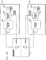
- FIGS. 2A , 2B and 2C are simplified block diagram illustrations of three alternative examples of the multiple antenna reading system of FIGS. 1A & 1B .
- reader 116 is preferably as shown in FIG. 5A as described hereinbelow.
- a pair of antenna modules 210 and 212 are coupled to reader 116, preferably by coaxial galvanic connections.
- Antenna module 210 includes an antenna coil 220, corresponding to either of antennas 110 and 112, which is coupled to reader 116 via antenna matching circuitry 221 and via a disabling circuit 222, which selectably effectively short circuits antenna coil 220 or otherwise changes its resonance frequency or Q factor.
- disabling circuit 222 may otherwise prevent generation of an RF field by the antenna.
- Antenna module 212 includes an antenna coil 226, corresponding to the other of antennas 110 and 112, which is coupled to reader 116 via antenna matching circuitry 227 and via a disabling circuit 228, which selectably effectively short circuits antenna coil 220 or otherwise changes its resonance frequency or Q factor.
- disabling circuit 222 may otherwise prevent generation of an RF field by the antenna.
- Antenna matching circuitry 221/227 is preferably of the type described in applicant/assignee's U.S. Pat. No. 5,241,160 .
- reader 116 is operative to provide a disable signal to disable circuit 228 during activation of antenna coil 220 and is operative to provide a disable signal to disable circuit 222 during activation of antenna coil 226.
- the disable signal provided to disable circuit 228 is operative to short circuit antenna coil 226 and the disable signal provided to disable circuit 222 is operative to short circuit antenna coil 220.
- reader 116 is preferably as shown in FIG. 5B as described hereinbelow.
- a pair of antenna modules 230 and 232 are coupled to reader 116, preferably by coaxial galvanic connections.
- Antenna module 230 includes an antenna coil 240, corresponding to either of antennas 110 and 112, which is coupled to reader 116 via antenna matching circuitry 241 and via a disable circuit 242, which selectably effectively short circuits antenna coil 240.
- Antenna module 232 includes an antenna coil 246, corresponding to the other of antennas 110 and 112, which is coupled to reader 116 via antenna matching circuitry 247 and via a disable circuit 248, which selectably effectively short circuits antenna coil 246.
- Antenna matching circuitry 241/247 is preferably of the type described in applicant/assignee's U.S. Pat. No. 5,241,160 .
- an RF signal output by reader 116 via the coaxial galvanic connection with antenna module 230 is rectified and employed to provide a disable signal to disable circuit 248 during activation of antenna coil 240 and an RF signal output by reader 116 via the coaxial galvanic connection with antenna module 232 is rectified and employed to provide a disable signal to disable circuit 242 during activation of antenna coil 246.
- the disable signal provided to disable circuit 248 is operative to short circuit antenna coil 246 and the disable signal provided to disable circuit 242 is operative to short circuit antenna coil 240.
- reader 116 is preferably as shown in FIG. 5C as described hereinbelow.
- a pair of antenna modules 250 and 252 are coupled to reader 116, preferably by coaxial galvanic connections.
- Antenna module 250 includes an antenna coil 260, corresponding to either of antennas 110 and 112, which is coupled to reader 116 via antenna matching circuitry 261 and via a disabling circuit 262, which selectably effectively short circuits antenna coil 260 in response to a disable signal received via a low pass filter 264.
- Antenna module 252 includes an antenna coil 266, corresponding to the other of antennas 110 and 112, which is coupled to reader 116 via antenna matching circuitry 267 and via a disabling circuit 268, which selectably effectively short circuits antenna coil 266 in response to a disable signal received via a low pass filter 269.
- Antenna matching circuitry 261/267 is preferably of the type described in applicant/assignee's U.S. Pat. No. 5,241,160 .
- the reader 116 provides superimposed RF and DC control signals along the coaxial galvanic connections with the antenna modules 250 and 252.
- the reader 116 includes a pair of low pass filters 270 and 271 which prevent the RF signals from being attenuated.
- reader 116 is operative to provide a disable signal to disable circuit 268 during activation of antenna coil 260 and is operative to provide a disable signal to disable circuit 262 during activation of antenna coil 266.
- the disable signal provided to disable circuit 268 is operative to short circuit antenna coil 266 and the disable signal provided to disable circuit 262 is operative to short circuit antenna coil 260.
- the DC control signals from the reader 116 are routed via the coaxial galvanic connections and low pass filters 264/269.
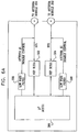
- FIG. 3 illustrates each of antenna modules 250 and 252 in the example of FIG. 2C . As seen in FIG.
- low pass filter 264/269 comprising an inductor 272, a resistor 274 and a capacitor 276 connected in series, is coupled between the signal input to the matching circuit 261/267 and ground.
- Resistor 274 controls the input current needed for activation of diode 280 of optocoupler 278.
- trace A illustrates the signal carried by the coaxial galvanic connection in antenna module 250
- trace B illustrates a DC control signal provided by reader 116 which is superimposed on the RF output of reader 116 to form the signal in trace A
- Trace C illustrates a DC signal output by the low pass filter 264 of antenna module 250. It is appreciated that the voltage of the DC signal in trace C is governed by resistor 274 in order to be suitable for diode 280 of optocoupler 278.
- Trace D illustrates the signal carried by the coaxial galvanic connection in antenna module 252.
- Trace E illustrates the second DC control signal provided by reader 116 which is superimposed on the RF output of reader 116 to form the signal in trace D.
- Trace F illustrates a DC signal output by the low pass filter 269 of antenna module 252.
- Low pass filter 269 blocks this RF signal with the result that a disable signal is not provided to switch 268 and when antenna coil 266 of antenna module 252 is not operating, a DC control signal from reader 116 is routed via the coaxial galvanic connection, passes through low pass filter 269 and is provided as a disable signal to switch 268.
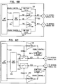
- FIGS. 5A , 5B and 5C are simplified illustrations of a reader useful in the systems of FIGS. 2A , 2B and 2C , respectively.
- a microcontroller 280 such as an MCS'51, interfaces with first and second RF transceivers 282 and 284, which are typically NXP RC531 chips, whose outputs are supplied to the antenna modules 210 and 212 respectively.
- Microcontroller 280 provides disable control signals to respective disabling circuits 222 and 228.
- a microcontroller 290 such as an MCS'51, interfaces with first and second RF transceivers 292 and 294, which are typically NXP RC531 chips, whose outputs appear as the RF portions of traces A and D respectively in FIG. 4 .
- a microcontroller 300 such as an MCS'51, interfaces with first and second RF transceivers 302 and 304, which are typically NXP RC531 chips, whose outputs appear as the RF portions of traces A and D respectively in FIG. 4 .
- Microcontroller 300 preferably provides two disable control signals which are routed via the coaxial galvanic connection to respective antenna modules 250 and 252, which appear as the DC portions of traces A and D respectively in FIG. 4 .
- Low pass filters 306 and 308 are provided to prevent the RF signals from being attenuated.
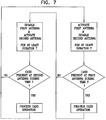
- FIG. 6 is a simplified flowchart illustrating operation of a system employing the circuitry of any of FIGS. 2A-2C .
- the reader 116 preferably activates a first antenna, which may be either of antennas 110 and 112 and generally simultaneously deactivates a second antenna, which is the other of antennas 110 and 112.
- the activation of the first antenna and corresponding deactivation of the second antenna is for a duration of at least a time T.
- Activation of the first antenna produces an RF field in the general region thereof and sends a smart card interrogation message superimposed on the RF field.
- this type of antenna functionality may be in accordance with the ISO/IEC 14443 Standard or the ISO/IEC 15693 Standard.
- a smart card such as one of cards 106, 107, 136 and 137, responds to the interrogation message from the first antenna within the time duration T, bidirectional communication is established between the reader 116 and the card, which may continue beyond time duration T. Upon termination of that communication, typically irrespective of the whether the card is removed from the RF field of the first antenna, the reader 116 deactivates the first antenna and generally simultaneously activates the second antenna.
- the reader 116 deactivates the first antenna and generally simultaneously activates the second antenna for a time duration T. Activation of the second antenna produces an RF field in the general region thereof and sends a smart card interrogation message superimposed on the RF field.
- a smart card such as one of cards 106, 107, 136 and 137, responds to the interrogation message from the second antenna within the time duration T, bidirectional communication is established between the reader 116 and the card, which may continue beyond time duration T. Upon termination of that communication, typically irrespective of the whether the card is removed from the RF field of the second antenna, the reader 116 deactivates the second antenna and generally simultaneously activates the first antenna.
- the reader 116 deactivates the second antenna and generally simultaneously activates the first antenna for a time duration T.
- time durations T need not all be the same.
- system of the present invention can operate with more than two antennas and that the functionality described hereinabove is readily adapted for multiple antenna operation. In such a case, more than one antenna may be activated simultaneously and more than one antenna may be deactivated simultaneously.
Landscapes
- Engineering & Computer Science (AREA)
- Health & Medical Sciences (AREA)
- Toxicology (AREA)
- Physics & Mathematics (AREA)
- Computer Networks & Wireless Communication (AREA)
- Electromagnetism (AREA)
- General Health & Medical Sciences (AREA)
- Artificial Intelligence (AREA)
- Computer Vision & Pattern Recognition (AREA)
- General Physics & Mathematics (AREA)
- Theoretical Computer Science (AREA)
- Near-Field Transmission Systems (AREA)
Description
- The present invention relates to contactless card reading systems and methodologies.
- The following patent publications are believed to represent the current state of the art:
-
U.S. Pat. Nos. 3,395,353 ;4,497,068 ;4,857,760 ;4,951,044 ;5,241,160 ;5,349,173 ;5,357,091 ;5,539,188 ;5,640,003 ;5,698,838 ;5,801,372 ;5,812,942 ;5,815,020 ;5,825,329 ;5,831,257 ;5,864,126 ;5,874,725 ;5,978,655 ;6,021,951 ;6,074,312 ;RE36769 ;6,161,762 ;6,202,927 ;6,209,592 ;6,234,902 ;6,329,139 ;6,375,082 ;6,445,743 ;6,507,130 ;6,517,000 ;6,533,178 ;6,601,770 ;6,686,847 ;6,769,604 ;6,883,103 ;7,064,651 ;7,075,434 ;7,091,412 ;7,162,302 ;7,183,929 ;7,207,488 ;7,260,221 ;7,280,970 ;7,334,735 and7,383,297 . -
US6617960A discloses apparatus for controlling access of persons, with access lanes adapted for the individual passage of these persons, with readers associated with the access lanes for access authorization and identification and/or blocking means for the persons. Between two adjacent access lanes there is provided a control device, which includes - when viewed in the passing direction - the identification and/or blocking means and the electronic components required for controlling these means, which are located to the left and to the right, respectively. -
US2006/165039A discloses a reader device for locating and tracking multiple tags including a plurality of closely packed antenna circuits and at least one controller configured to control the plurality of closely packed antenna circuits. The at least one controller is configured to activate one or more of the antenna circuits to generate at least one resonance signal field configured to interrogate at least one tag associated with the one or more active antenna circuits while substantially preventing or reducing cross-coupling of signals between the one or more active antenna circuits and at least one antenna circuit within the at least one resonance signal field to a sufficiently low level, wherein the sufficiently low level substantially prevents misreads from unwanted tags, to thereby track the multiple tags in a substantially controlled manner. -
EP1892676A discloses a system that has antenna coils, which are attached to a reading device and arranged one behind the other at an access track. The coils with capacitances form resonant circuits. One of the resonant circuits is controlled by the reading device for reading the data for an access authorization from a transponder, which is carried by a user. - The present invention seeks to provide improved contactless card reading systems and methodologies.
- There is thus provided in accordance with a preferred embodiment of the present invention a multiple antenna reading system suitable for use with contactless transaction devices, the system comprising: at least one reader; a first antenna module comprising a first antenna and first antenna function disabling circuitry; a second antenna module comprising a second antenna and second antenna function disabling circuitry; said first and second antennas having at least some inductive coupling therebetween and being operatively connected to said at least one reader; wherein the first and second antenna modules are arranged such that an RF signal output by reader to said first antenna module is rectified and employed to provide a disable signal to said second antenna function disabling circuitry during activation of said first antenna and an RF signal output by reader to said second antenna module is rectified and employed to provide a disable signal to said first antenna function disabling circuitry during activation of said second antenna.
- Preferably, the activation of one of the first and second antennas includes generation of an RF field by the one of the first and second antennas as a result of an RF signal generated by the reader.
- Preferably, the at least one reader also includes at least one of communication, computation and logic functionalities. In accordance with a preferred embodiment of the present invention, each of the at least first and second antennas are arranged to communicate with a smart card.
- In accordance with a preferred embodiment of the present invention, the at least first and second antennas are associated with access control functionality. Additionally or alternatively, the at least first and second antennas are associated with identification functionality. Alternatively or additionally, the at least first and second antennas are associated with payment functionality.
- Preferably, each of the at least first and second antennas includes an antenna coil and antenna matching circuitry.
- In accordance with a preferred embodiment of the present invention, the antenna function disabling circuitry is operative to selectably effectively short circuit the antenna coil. Alternatively, the antenna function disabling circuitry is operative to selectably change a resonant frequency of the antenna coil. Alternatively, the antenna function disabling circuitry is operative to selectably change the Q-factor of the antenna coil.
- In accordance with a preferred embodiment of the present invention, the reader includes at least first and second low pass filters operative to prevent the RF signals from being attenuated.
- In accordance with a preferred embodiment of the present invention, each of the at least first and second antennas also includes a low pass filter. Additionally, the low pass filter includes an inductor, a resistor and a capacitor connected in series.
- Preferably, the at least one reader includes a microcontroller and at least a first and a second RF transceivers.
- In accordance with a preferred embodiment of the present invention, the at least first and second antennas include more than two antennas and antenna function disabling circuitry operates with the more than two antennas such that more than one antenna may be activated simultaneously and more than one antenna may be deactivated simultaneously. Additionally or alternatively, the at least one reader includes multiple readers connected to multiple one of the at least first and second antennas and more than one antenna may be activated simultaneously and more than one antenna may be deactivated simultaneously.
- In accordance with a preferred embodiment of the present invention, the at least one reader includes multiple readers, the at least first antenna is coupled to a first reader of the multiple readers and the at least second antenna is coupled to a second reader of the multiple readers. Alternatively, the at least one reader includes one reader and the at least first antenna and the at least second antenna are coupled to the one reader.
- The present invention will be understood and appreciated more fully from the following detailed description, taken in conjunction with the drawings in which:
-
FIG. 1A is a simplified, partially-pictorial, partially block diagram illustration of a contactless card reading system constructed and operative in accordance with a preferred embodiment of the present invention in the context of a transportation system; -
FIG. 1B is a simplified, partially-pictorial, partially block diagram illustration of a contactless card reading system constructed and operative in accordance with a preferred embodiment of the present invention in the context of an access control system; -
FIGS. 2A and2C are simplified block diagram illustrations of alternative multiple antenna reading systems useful in the systems ofFIGS. 1A & 1B ; -
FIG. 2B is a simplified block diagram illustration of an embodiment of the invention. -
FIG. 3 is a simplified circuit diagram of an antenna module in the system ofFIG. 2C ; -
FIG. 4 is a simplified signal diagram corresponding to the operation of the system ofFIG. 3 ; -
FIGS. 5A ,5B and 5C are simplified illustrations of a reader useful in the systems ofFIGS. 2A ,2B and2C respectively; and -
FIG. 6 is a simplified flowchart illustrating some features of the operation of the systems of any ofFIGS. 2A-2C . - Reference is now made to
FIG. 1A , which is a simplified, partially-pictorial, partially block diagram illustration of a contactless card reading system constructed and operative in accordance with a preferred embodiment of the present invention in the context of a transportation system. - As seen in
FIG. 1A , there is provided aturnstile 100 having acentral pillar 102 and a pair ofrotatable turnstile turrets smart cards passages turnstile turrets antennas pillar 102. - Due to a desire to minimize the width of
pillar 102,antennas Antennas more reader 116. The term "reader" is used herein in a broad sense and includes a conventional contactless reader as well as optional communication, computation and logic functionalities. -
Antenna 110 is arranged to read asmart card 106 of a person passing throughpassage 108, whileantenna 112 is arranged to read asmart card 107 of a person passing throughpassage 109. It is appreciated that it is unacceptable thatsmart card 106 placedadjacent antenna 110 be read instead byantenna 112 and thus operateturret 105 instead ofturret 104. - It is further appreciated that typically
smart cards smart cards - It is a particular feature of the present invention that there is provided antenna
function disabling circuitry 120, which is automatically operative upon activation of at least a first one of theantennas antennas contactless card 106 atantenna 112. - Antenna
function disabling circuitry 120 typically includes circuitry associated with each ofantennas reader 116. Alternatively, antennafunction disabling circuitry 120 need not be associated withreader 116. -
Antennas reader 116 and antennafunction disabling circuitry 120 are together referred to as a multiple antenna reading system. - Reference is now made to
FIG. 1B , which is a simplified, partially-pictorial, partially block diagram illustration of a contactless card reading system constructed and operative in accordance with a preferred embodiment of the present invention in the context of an access control system. For the sake of convenience and clarity, items in the embodiment ofFIG. 1B which may be identical to those described above in the embodiment ofFIG. 1A are given identical reference numbers. - As seen in
FIG. 1B , there is provided a bi-directional accesscontrol terminal assembly 130 associated with adoor lock 132 of adoor 134. The bi-directional accesscontrol terminal assembly 130 governs passage of persons, each bearing a contactless card, such asaccess control cards door 134. The operation ofdoor lock 132 is governed by access control circuitry forming part ofassembly 130 and including a pair ofantennas wall 138adjacent door 134. - In practice,
antennas Antennas more reader 116. The term "reader" is used herein in a broad sense and includes a conventional contactless reader as well as optional communication, computation and logic functionalities. -
Antenna 110 is arranged to read asmart card 136 of a person passing throughdoor 134 in a first direction, whileantenna 112 is arranged to read asmart card 137 of a person passing throughdoor 134 in a direction opposite to the first direction. It is appreciated that it is unacceptable thatsmart card 136 placedadjacent antenna 110 be read instead byantenna 112 and thus register access in an incorrect direction. - It is further appreciated that typically
smart cards card 136 may be entitled to pass throughdoor 134 in one direction but not in the other. - As in the embodiment of
FIG. 1A , it is a particular feature of the present invention that there is provided antennafunction disabling circuitry 120, which is automatically operative upon activation of at least a first one of theantennas antennas contactless card 106 atantenna 112. - Antenna
function disabling circuitry 120 typically includes circuitry associated with each ofantennas reader 116. Alternatively, antennafunction disabling circuitry 120 need not be associated withreader 116. Various examples of antennafunction disabling circuitry 120 will now be described with reference toFIGS. 2A-2C . -
Antennas reader 116 and antennafunction disabling circuitry 120 are together referred to as a multiple antenna reading system. - Reference is now made to
FIGS. 2A ,2B and2C are simplified block diagram illustrations of three alternative examples of the multiple antenna reading system ofFIGS. 1A & 1B . - In the example of
FIG. 2A ,reader 116 is preferably as shown inFIG. 5A as described hereinbelow. A pair ofantenna modules reader 116, preferably by coaxial galvanic connections.Antenna module 210 includes anantenna coil 220, corresponding to either ofantennas reader 116 viaantenna matching circuitry 221 and via a disablingcircuit 222, which selectably effectively shortcircuits antenna coil 220 or otherwise changes its resonance frequency or Q factor. Alternatively, disablingcircuit 222 may otherwise prevent generation of an RF field by the antenna. -
Antenna module 212 includes anantenna coil 226, corresponding to the other ofantennas reader 116 viaantenna matching circuitry 227 and via a disablingcircuit 228, which selectably effectively shortcircuits antenna coil 220 or otherwise changes its resonance frequency or Q factor. Alternatively, disablingcircuit 222 may otherwise prevent generation of an RF field by the antenna. -
Antenna matching circuitry 221/227 is preferably of the type described in applicant/assignee'sU.S. Pat. No. 5,241,160 . - It is a particular feature of this example that
reader 116 is operative to provide a disable signal to disablecircuit 228 during activation ofantenna coil 220 and is operative to provide a disable signal to disablecircuit 222 during activation ofantenna coil 226. The disable signal provided to disablecircuit 228 is operative to shortcircuit antenna coil 226 and the disable signal provided to disablecircuit 222 is operative to shortcircuit antenna coil 220. - In the embodiment of the invention
FIG. 2B ,reader 116 is preferably as shown inFIG. 5B as described hereinbelow. A pair ofantenna modules reader 116, preferably by coaxial galvanic connections.Antenna module 230 includes anantenna coil 240, corresponding to either ofantennas reader 116 viaantenna matching circuitry 241 and via a disablecircuit 242, which selectably effectively shortcircuits antenna coil 240.Antenna module 232 includes anantenna coil 246, corresponding to the other ofantennas reader 116 viaantenna matching circuitry 247 and via a disablecircuit 248, which selectably effectively shortcircuits antenna coil 246. -
Antenna matching circuitry 241/247 is preferably of the type described in applicant/assignee'sU.S. Pat. No. 5,241,160 . - It is a particular feature of the present invention that an RF signal output by
reader 116 via the coaxial galvanic connection withantenna module 230 is rectified and employed to provide a disable signal to disablecircuit 248 during activation ofantenna coil 240 and an RF signal output byreader 116 via the coaxial galvanic connection withantenna module 232 is rectified and employed to provide a disable signal to disablecircuit 242 during activation ofantenna coil 246. The disable signal provided to disablecircuit 248 is operative to shortcircuit antenna coil 246 and the disable signal provided to disablecircuit 242 is operative to shortcircuit antenna coil 240. - In the example of
FIG. 2C ,reader 116 is preferably as shown in FIG. 5C as described hereinbelow. A pair ofantenna modules reader 116, preferably by coaxial galvanic connections.Antenna module 250 includes anantenna coil 260, corresponding to either ofantennas reader 116 viaantenna matching circuitry 261 and via a disablingcircuit 262, which selectably effectively shortcircuits antenna coil 260 in response to a disable signal received via alow pass filter 264. -
Antenna module 252 includes anantenna coil 266, corresponding to the other ofantennas reader 116 viaantenna matching circuitry 267 and via a disablingcircuit 268, which selectably effectively shortcircuits antenna coil 266 in response to a disable signal received via alow pass filter 269. -
Antenna matching circuitry 261/267 is preferably of the type described in applicant/assignee'sU.S. Pat. No. 5,241,160 . - It is a particular feature of this example that the
reader 116 provides superimposed RF and DC control signals along the coaxial galvanic connections with theantenna modules reader 116 includes a pair of low pass filters 270 and 271 which prevent the RF signals from being attenuated. - It is a particular feature of this example that
reader 116 is operative to provide a disable signal to disablecircuit 268 during activation ofantenna coil 260 and is operative to provide a disable signal to disablecircuit 262 during activation ofantenna coil 266. The disable signal provided to disablecircuit 268 is operative to shortcircuit antenna coil 266 and the disable signal provided to disablecircuit 262 is operative to shortcircuit antenna coil 260. In the example ofFIG. 2C , the DC control signals from thereader 116 are routed via the coaxial galvanic connections and low pass filters 264/269. Reference is now made toFIG. 3 which illustrates each ofantenna modules FIG. 2C . As seen inFIG. 3 ,low pass filter 264/269, comprising aninductor 272, aresistor 274 and acapacitor 276 connected in series, is coupled between the signal input to thematching circuit 261/267 and ground. An output of thelow pass filter 264/269, preferably at the junction ofresistor 274 andcapacitor 276, serves as a disable signal supplied to disablecircuit 262/268, which is preferably anoptocoupler 278.Resistor 274 controls the input current needed for activation ofdiode 280 ofoptocoupler 278. - Reference is now made to
FIG. 4 , which illustrates the operation of the circuitry ofFIGS. 2C and3 . With particular reference to the example shown inFIG. 2C , inFIG. 4 , trace A illustrates the signal carried by the coaxial galvanic connection inantenna module 250, trace B illustrates a DC control signal provided byreader 116 which is superimposed on the RF output ofreader 116 to form the signal in trace A. Trace C illustrates a DC signal output by thelow pass filter 264 ofantenna module 250. It is appreciated that the voltage of the DC signal in trace C is governed byresistor 274 in order to be suitable fordiode 280 ofoptocoupler 278. Trace D illustrates the signal carried by the coaxial galvanic connection inantenna module 252. Trace E illustrates the second DC control signal provided byreader 116 which is superimposed on the RF output ofreader 116 to form the signal in trace D. Trace F illustrates a DC signal output by thelow pass filter 269 ofantenna module 252. - As seen in
FIG. 3 and atFIG. 4 in traces A and C, whenantenna coil 260 ofantenna module 250 is operating, an RF signal is carried by the coaxial galvanic connection.Low pass filter 264 blocks this RF signal with the result that a disable signal is not provided to switch 262 and whenantenna coil 260 ofantenna module 250 is not operating, a DC control signal fromreader 116 is routed via the coaxial galvanic connection, passes throughlow pass filter 264 and is provided as a disable signal to switch 262. - As further seen in
FIG. 3 and atFIG. 4 in traces D and F, whenantenna coil 266 ofantenna module 252 is operating, an RF signal is carried by the coaxial galvanic connection.Low pass filter 269 blocks this RF signal with the result that a disable signal is not provided to switch 268 and whenantenna coil 266 ofantenna module 252 is not operating, a DC control signal fromreader 116 is routed via the coaxial galvanic connection, passes throughlow pass filter 269 and is provided as a disable signal to switch 268. - Reference is now made to
FIGS. 5A ,5B and 5C, which are simplified illustrations of a reader useful in the systems ofFIGS. 2A ,2B and2C , respectively. In the embodiment ofFIG. 5A , amicrocontroller 280, such as an MCS'51, interfaces with first andsecond RF transceivers antenna modules Microcontroller 280 provides disable control signals to respective disablingcircuits - In the embodiment of
FIG. 5B , amicrocontroller 290, such as an MCS'51, interfaces with first andsecond RF transceivers FIG. 4 . - In the embodiment of FIG. 5C, a
microcontroller 300, such as an MCS'51, interfaces with first andsecond RF transceivers FIG. 4 .Microcontroller 300 preferably provides two disable control signals which are routed via the coaxial galvanic connection torespective antenna modules FIG. 4 . Low pass filters 306 and 308 are provided to prevent the RF signals from being attenuated. - Reference is now made to
FIG. 6 , which is a simplified flowchart illustrating operation of a system employing the circuitry of any ofFIGS. 2A-2C . - As seen in
FIG. 6 , thereader 116 preferably activates a first antenna, which may be either ofantennas antennas - If a smart card such as one of
cards reader 116 and the card, which may continue beyond time duration T. Upon termination of that communication, typically irrespective of the whether the card is removed from the RF field of the first antenna, thereader 116 deactivates the first antenna and generally simultaneously activates the second antenna. - However, if a smart card such as one of
cards reader 116 deactivates the first antenna and generally simultaneously activates the second antenna for a time duration T. Activation of the second antenna produces an RF field in the general region thereof and sends a smart card interrogation message superimposed on the RF field. - If a smart card such as one of
cards reader 116 and the card, which may continue beyond time duration T. Upon termination of that communication, typically irrespective of the whether the card is removed from the RF field of the second antenna, thereader 116 deactivates the second antenna and generally simultaneously activates the first antenna. - However, if a smart card such as one of
cards reader 116 deactivates the second antenna and generally simultaneously activates the first antenna for a time duration T. - It is appreciated that the time durations T need not all be the same.
- It is further appreciated that the system of the present invention can operate with more than two antennas and that the functionality described hereinabove is readily adapted for multiple antenna operation. In such a case, more than one antenna may be activated simultaneously and more than one antenna may be deactivated simultaneously.
- It will be appreciated by persons skilled in the art that the present invention is not limited by what has been particularly shown and described hereinabove. Rather the scope of the present invention includes both combinations and subcombinations of various features described hereinabove and variations and modifications thereof which are not shown in the prior art.
Claims (13)
- A multiple antenna reading system suitable for use with contactless transaction devices, said system comprising:at least one reader (116);a first antenna module (230) comprising a first antenna (240) and first antenna function disabling circuitry (242);a second antenna module (232) comprising a second antenna (246) and second antenna function disabling circuitry (248);said first and second antennas having at least some inductive coupling therebetween and being operatively connected to said at least one reader (116); characterised in that the first and second antenna modules are arranged such that an RF signal output by reader (116) to said first antenna module (230) is rectified and employed to provide a disable signal to said second antenna function disabling circuitry (248) during activation of said first antenna (240) and an RF signal output by reader (116) to said second antenna module (232) is rectified and employed to provide a disable signal to said first antenna function disabling circuitry (242) during activation of said second antenna (246).
- A multiple antenna reading system according to claim 1 wherein said activation of one of said first and second antennas (240, 246) comprises generation of an RF field by said one of said first and second antennas (240, 246) as a result of a signal generated by said reader (116).
- A multiple antenna reading system according to claim 1 wherein said at least one reader (116) also comprises at least one of communication, computation and logic functionalities.
- A multiple antenna reading system according to claim 1 wherein each of said at least first and second antennas (240,246) are arranged to communicate with a smart card (106,107).
- A multiple antenna reading system according to claim 1 wherein said system is at least part of an access control system or an identification system or a payment system.
- A multiple antenna reading system according to claim 1 wherein each of said at least first and second antennas comprises an antenna coil and antenna matching circuitry (241, 247).
- A multiple antenna reading system according to claim 6 wherein said antenna function disabling circuitry (242, 248) is operative to selectably effectively short circuit said antenna coil (240, 246).
- A multiple antenna reading system according to claim 6 wherein said antenna function disabling circuitry (242, 248) is operative to selectably change a resonant frequency of said antenna coil (240, 246).
- A multiple antenna reading system according to claim 6 wherein said antenna function disabling circuitry (242, 248) is operative to selectably change the Q -factor of said antenna coil (240, 246).
- A multiple antenna reading system according to claim 1 wherein said at least one reader comprises a microcontroller and at least a first and a second RF transceivers.
- A multiple antenna reading system according to claim 1 wherein said at least first and second antennas comprise more than two antennas and antenna function disabling circuitry operates with said more than two antennas such that more than one antenna may be activated simultaneously and more than one antenna may be deactivated simultaneously.
- A multiple antenna reading system according to claim 1 wherein said at least one reader comprises multiple readers connected to multiple ones of said at least first and second antennas and more than one antenna may be activated simultaneously and more than one antenna may be deactivated simultaneously.
- A multiple antenna reading system according to claim 1 wherein:said at least one reader comprises multiple readers;said at least first antenna is operatively connected to a first reader of said multiple readers; andsaid at least second antenna is operatively connected to a second reader of said multiple readers.
Applications Claiming Priority (2)
| Application Number | Priority Date | Filing Date | Title |
|---|---|---|---|
| US12/707,448 US8313028B2 (en) | 2010-02-17 | 2010-02-17 | Multiple antenna reading system suitable for use with contactless transaction devices |
| PCT/IL2011/000168 WO2011101850A1 (en) | 2010-02-17 | 2011-02-17 | Multiple antenna reading system suitable for use with contactless transaction devices |
Publications (3)
| Publication Number | Publication Date |
|---|---|
| EP2537121A1 EP2537121A1 (en) | 2012-12-26 |
| EP2537121A4 EP2537121A4 (en) | 2013-10-16 |
| EP2537121B1 true EP2537121B1 (en) | 2016-04-13 |
Family
ID=44368949
Family Applications (1)
| Application Number | Title | Priority Date | Filing Date |
|---|---|---|---|
| EP11744358.0A Not-in-force EP2537121B1 (en) | 2010-02-17 | 2011-02-17 | Multiple antenna reading system suitable for use with contactless transaction devices |
Country Status (8)
| Country | Link |
|---|---|
| US (1) | US8313028B2 (en) |
| EP (1) | EP2537121B1 (en) |
| JP (1) | JP2013519960A (en) |
| CN (1) | CN102741857A (en) |
| AU (1) | AU2011216860B2 (en) |
| CA (1) | CA2789873A1 (en) |
| WO (1) | WO2011101850A1 (en) |
| ZA (1) | ZA201206188B (en) |
Families Citing this family (9)
| Publication number | Priority date | Publication date | Assignee | Title |
|---|---|---|---|---|
| US8981907B1 (en) * | 2012-07-19 | 2015-03-17 | Disney Enterprises, Inc. | RFID antenna multiplexing |
| JP6425379B2 (en) * | 2012-12-27 | 2018-11-21 | ジーエヌ ヒアリング エー/エスGN Hearing A/S | Hearing device with power management and related method |
| US9575156B2 (en) | 2013-01-15 | 2017-02-21 | Disney Enterprises, Inc. | Spatial recognition of RFID tag placement using antenna multiplexing |
| US9760747B2 (en) * | 2014-03-11 | 2017-09-12 | Canon Kabushiki Kaisha | Communication apparatus and method for controlling the same |
| JP6413459B2 (en) * | 2014-08-08 | 2018-10-31 | 株式会社デンソーウェーブ | Card reader |
| JP6438245B2 (en) * | 2014-09-05 | 2018-12-12 | キヤノン株式会社 | COMMUNICATION DEVICE, ITS CONTROL METHOD, PROGRAM |
| US9577718B2 (en) * | 2014-11-19 | 2017-02-21 | Qualcomm Incorporated | Systems and methods for inductively coupled communications |
| WO2018227118A1 (en) | 2017-06-09 | 2018-12-13 | Carrier Corporation | Method of adjusting bluetooth connectivity for expediting access controls |
| CN112635991A (en) * | 2019-10-08 | 2021-04-09 | 中兴通讯股份有限公司 | Antenna, antenna power supply method, antenna single feed combination method and device |
Family Cites Families (57)
| Publication number | Priority date | Publication date | Assignee | Title |
|---|---|---|---|---|
| US3395353A (en) | 1966-04-18 | 1968-07-30 | Sperry Rand Corp | Pulse width discriminator |
| US4497068A (en) | 1982-01-25 | 1985-01-29 | Eaton Corporation | Encoding system for optic data link |
| US4857760A (en) | 1988-02-10 | 1989-08-15 | Tektronix, Inc. | Bipolar glitch detector circuit |
| US4951044A (en) | 1989-03-21 | 1990-08-21 | Motorola, Inc. | Paging terminal apparatus with user selectable page forwarding capability and methodology therefor |
| US5241160A (en) | 1990-12-28 | 1993-08-31 | On Track Innovations Ltd. | System and method for the non-contact transmission of data |
| DK0510220T3 (en) | 1991-04-23 | 1997-02-17 | Siemens Ag | |
| JPH04329415A (en) | 1991-04-30 | 1992-11-18 | Fujitsu Ltd | Card type input/output interface device |
| FR2685519A1 (en) | 1991-12-20 | 1993-06-25 | Gemplus Card Int | SYSTEM FOR THE IDENTIFICATION OF CONTAINERS, ESPECIALLY GAS BOTTLES. |
| EP0646983B1 (en) | 1993-10-04 | 1998-09-02 | Amtech Corporation | Modulated backscatter microstrip patch antenna |
| JP3201157B2 (en) | 1994-07-26 | 2001-08-20 | 松下電器産業株式会社 | IC card device |
| JPH0962816A (en) | 1994-10-06 | 1997-03-07 | Mitsubishi Electric Corp | Contactless IC card and contactless IC card system including the same |
| JPH08139516A (en) | 1994-11-08 | 1996-05-31 | Toshiba Corp | Information processing device |
| US6329139B1 (en) | 1995-04-25 | 2001-12-11 | Discovery Partners International | Automated sorting system for matrices with memory |
| US5786763A (en) * | 1996-06-20 | 1998-07-28 | Sensormatic Electronics Corporation | Antenna multiplexer with isolation of switching elements |
| US5812942A (en) | 1996-09-24 | 1998-09-22 | Motorola, Inc. | Balanced differential radio receiver and method of operation |
| US5815020A (en) | 1996-09-24 | 1998-09-29 | Motorola, Inc. | Balance differential receiver |
| US5864126A (en) | 1996-12-11 | 1999-01-26 | Ncr Corporation | Self reading permanent electronic label for a computing device |
| JP4143158B2 (en) | 1997-04-16 | 2008-09-03 | 聯華電子股▲ふん▼有限公司 | Data carrier |
| JPH10320519A (en) | 1997-05-19 | 1998-12-04 | Rohm Co Ltd | Transponder in IC card communication system |
| US6074312A (en) | 1997-07-28 | 2000-06-13 | Dynamic Solutions International | Golf handicap system and methods |
| JP3475996B2 (en) | 1997-10-07 | 2003-12-10 | インターナショナル・ビジネス・マシーンズ・コーポレーション | Non-contact IC card system, IC card reader and IC card |
| IL122841A0 (en) | 1997-12-31 | 1998-08-16 | On Track Innovations Ltd | Smart card for effecting data transfer using multiple protocols |
| ATE311696T1 (en) | 1998-02-17 | 2005-12-15 | Koninkl Philips Electronics Nv | TRANSMIT/RECEIVE STATION WITH IMPEDANCE-MATCHED RECEIVING MEANS FOR TRANSPONDER RESPONSE SIGNALS |
| US6617960B1 (en) | 1998-02-18 | 2003-09-09 | Teamaxess Ticketing Gmbh | Arrangement for controlling access of persons, and access terminal |
| US6075312A (en) * | 1998-03-17 | 2000-06-13 | Smart Biotechnology Co., Ltd. | Main structure for catching flow-injection type piezoelectric sensor |
| DE69940834D1 (en) | 1998-03-24 | 2009-06-10 | Toshiba Kk | Portable electronic device with contact and contactless interfaces |
| IL123949A (en) | 1998-04-03 | 2001-07-24 | On Track Innovations Ltd | Data transaction card having extended range |
| IL124424A0 (en) | 1998-05-11 | 1998-12-06 | On Track Innovations Ltd | Self-closing cap including an integral smart card |
| DE19845065A1 (en) | 1998-05-15 | 1999-11-25 | Siemens Ag | Contactless data transmission arrangement |
| IL125221A0 (en) | 1998-07-06 | 1999-03-12 | Toy Control Ltd | Motion activation using passive sound source |
| ES2198938T3 (en) * | 1998-08-14 | 2004-02-01 | 3M Innovative Properties Company | APPLICATION FOR A RADIO FREQUENCY IDENTIFICATION SYSTEM. |
| IL127569A0 (en) | 1998-09-16 | 1999-10-28 | Comsense Technologies Ltd | Interactive toys |
| US7334735B1 (en) | 1998-10-02 | 2008-02-26 | Beepcard Ltd. | Card for interaction with a computer |
| DE19850293A1 (en) | 1998-10-30 | 2000-05-04 | Koninkl Philips Electronics Nv | Media with protection against compromise |
| US7260221B1 (en) | 1998-11-16 | 2007-08-21 | Beepcard Ltd. | Personal communicator authentication |
| US6517000B1 (en) | 1999-05-03 | 2003-02-11 | Psc Scanning, Inc. | Dual ended cable for connecting electronic article surveillance antenna with RFID equipment |
| US7280970B2 (en) | 1999-10-04 | 2007-10-09 | Beepcard Ltd. | Sonic/ultrasonic authentication device |
| US7064651B2 (en) | 2000-04-12 | 2006-06-20 | Goetz Joseph R | Automatic vehicle theft prevention system |
| US6686847B1 (en) | 2000-05-12 | 2004-02-03 | Hewlett-Packard Development Company, L.P. | Indicator with daylight visibility using a single light emitting diode |
| JP2003535536A (en) | 2000-05-31 | 2003-11-25 | コーニンクレッカ フィリップス エレクトロニクス エヌ ヴィ | A data carrier for adapting the wearout interval to its own power consumption |
| JP2005519491A (en) * | 2002-01-09 | 2005-06-30 | ミードウエストベココーポレーション | Intelligent station using a plurality of RF antennas, and inventory control system and inventory control method incorporating the same |
| US7091412B2 (en) | 2002-03-04 | 2006-08-15 | Nanoset, Llc | Magnetically shielded assembly |
| US7162302B2 (en) | 2002-03-04 | 2007-01-09 | Nanoset Llc | Magnetically shielded assembly |
| JP2004046773A (en) | 2002-05-21 | 2004-02-12 | Nec Infrontia Corp | History management system |
| US7686229B2 (en) * | 2003-01-30 | 2010-03-30 | Hewlett-Packard Development Company, L.P. | RFID reader device having closely packed antennas |
| US7075434B2 (en) | 2003-09-22 | 2006-07-11 | Michael Shafir | Encoding and decoding method and system |
| JP4329932B2 (en) * | 2004-06-04 | 2009-09-09 | 日本信号株式会社 | Transceiver |
| KR100630823B1 (en) * | 2004-11-02 | 2006-10-02 | 주식회사 현대오토넷 | Radio wave identification tag device for tire in radio wave identification system |
| US7207488B2 (en) | 2004-11-04 | 2007-04-24 | Precision Dynamics Corproation | Combined barcode scanner and radio frequency identification reader with field interpretation array |
| JP4660219B2 (en) * | 2005-02-01 | 2011-03-30 | パナソニック株式会社 | Non-contact communication reader device |
| US7205896B2 (en) * | 2005-02-23 | 2007-04-17 | G-Time Electronic Co., Ltd. | RFID reader having multi-dimensional antenna array |
| JP4166772B2 (en) * | 2005-09-01 | 2008-10-15 | 株式会社日立国際電気 | Reader / writer device |
| EP1892676A1 (en) * | 2006-08-08 | 2008-02-27 | SkiData AG | Access control system |
| US7979033B2 (en) * | 2006-12-29 | 2011-07-12 | Broadcom Corporation | IC antenna structures and applications thereof |
| US7969364B2 (en) * | 2007-05-31 | 2011-06-28 | Frank Kriebel | Radio frequency device and method of manufacture |
| JP2009230512A (en) * | 2008-03-24 | 2009-10-08 | Sanden Corp | Rfid tag reader |
| US8099064B2 (en) * | 2008-05-08 | 2012-01-17 | Research In Motion Limited | Mobile wireless communications device with reduced harmonics resulting from metal shield coupling |
-
2010
- 2010-02-17 US US12/707,448 patent/US8313028B2/en active Active
-
2011
- 2011-02-17 AU AU2011216860A patent/AU2011216860B2/en not_active Ceased
- 2011-02-17 WO PCT/IL2011/000168 patent/WO2011101850A1/en not_active Ceased
- 2011-02-17 CN CN2011800074546A patent/CN102741857A/en active Pending
- 2011-02-17 EP EP11744358.0A patent/EP2537121B1/en not_active Not-in-force
- 2011-02-17 JP JP2012553442A patent/JP2013519960A/en active Pending
- 2011-02-17 CA CA2789873A patent/CA2789873A1/en not_active Abandoned
-
2012
- 2012-08-16 ZA ZA2012/06188A patent/ZA201206188B/en unknown
Also Published As
| Publication number | Publication date |
|---|---|
| US20110198398A1 (en) | 2011-08-18 |
| EP2537121A4 (en) | 2013-10-16 |
| CN102741857A (en) | 2012-10-17 |
| CA2789873A1 (en) | 2011-08-25 |
| AU2011216860B2 (en) | 2015-09-24 |
| ZA201206188B (en) | 2013-05-29 |
| EP2537121A1 (en) | 2012-12-26 |
| US8313028B2 (en) | 2012-11-20 |
| WO2011101850A1 (en) | 2011-08-25 |
| JP2013519960A (en) | 2013-05-30 |
| AU2011216860A1 (en) | 2012-09-13 |
Similar Documents
| Publication | Publication Date | Title |
|---|---|---|
| EP2537121B1 (en) | Multiple antenna reading system suitable for use with contactless transaction devices | |
| EP2250631B1 (en) | Methods and apparatus for preserving privacy in an rfid system | |
| EP2286520B1 (en) | Antenna design and interrogator system | |
| US7843345B2 (en) | Dual frequency RFID circuit | |
| US11734670B2 (en) | Detachable radio frequency identification switch tag | |
| US20140197991A1 (en) | Spatial recognition of rfid tag placement using antenna multiplexing | |
| US11809937B2 (en) | Detachable radio frequency identification switch tag | |
| US12265867B2 (en) | Detachable radio frequency identification switch tag | |
| US9787137B2 (en) | Power supply apparatus for providing a voltage from an electromagnetic field | |
| CN109428630A (en) | For driving the circuit and method of the antenna of NFC device | |
| KR101003827B1 (en) | Contactless Recognition Card with Multiple Rfid Chips | |
| KR20100044781A (en) | Method and device for the contact-free transmission of data from and/or to a plurality of data or information carriers, preferably in the form of reid tags | |
| US10885418B2 (en) | Detachable radio frequency identification switch tag | |
| US8981907B1 (en) | RFID antenna multiplexing | |
| KR20150014715A (en) | Both Sides Radio Frequency Communication Tag |
Legal Events
| Date | Code | Title | Description |
|---|---|---|---|
| PUAI | Public reference made under article 153(3) epc to a published international application that has entered the european phase |
Free format text: ORIGINAL CODE: 0009012 |
|
| 17P | Request for examination filed |
Effective date: 20120912 |
|
| AK | Designated contracting states |
Kind code of ref document: A1 Designated state(s): AL AT BE BG CH CY CZ DE DK EE ES FI FR GB GR HR HU IE IS IT LI LT LU LV MC MK MT NL NO PL PT RO RS SE SI SK SM TR |
|
| RIN1 | Information on inventor provided before grant (corrected) |
Inventor name: ITAY, NEHEMYA Inventor name: GILBOA, RONNIE Inventor name: BASHAN, ODED |
|
| RIN1 | Information on inventor provided before grant (corrected) |
Inventor name: GILBOA, RONNIE Inventor name: ITAY, NEHEMYA Inventor name: BASHAN, ODED |
|
| DAX | Request for extension of the european patent (deleted) | ||
| A4 | Supplementary search report drawn up and despatched |
Effective date: 20130918 |
|
| RIC1 | Information provided on ipc code assigned before grant |
Ipc: G06K 7/00 20060101AFI20130912BHEP Ipc: H01Q 7/00 20060101ALI20130912BHEP Ipc: H01Q 1/52 20060101ALI20130912BHEP Ipc: H01Q 1/22 20060101ALI20130912BHEP |
|
| REG | Reference to a national code |
Ref country code: HK Ref legal event code: DE Ref document number: 1180423 Country of ref document: HK |
|
| 17Q | First examination report despatched |
Effective date: 20140731 |
|
| GRAP | Despatch of communication of intention to grant a patent |
Free format text: ORIGINAL CODE: EPIDOSNIGR1 |
|
| INTG | Intention to grant announced |
Effective date: 20150928 |
|
| GRAS | Grant fee paid |
Free format text: ORIGINAL CODE: EPIDOSNIGR3 |
|
| GRAA | (expected) grant |
Free format text: ORIGINAL CODE: 0009210 |
|
| AK | Designated contracting states |
Kind code of ref document: B1 Designated state(s): AL AT BE BG CH CY CZ DE DK EE ES FI FR GB GR HR HU IE IS IT LI LT LU LV MC MK MT NL NO PL PT RO RS SE SI SK SM TR |
|
| REG | Reference to a national code |
Ref country code: GB Ref legal event code: FG4D |
|
| REG | Reference to a national code |
Ref country code: AT Ref legal event code: REF Ref document number: 790841 Country of ref document: AT Kind code of ref document: T Effective date: 20160415 Ref country code: CH Ref legal event code: EP |
|
| REG | Reference to a national code |
Ref country code: IE Ref legal event code: FG4D |
|
| REG | Reference to a national code |
Ref country code: DE Ref legal event code: R096 Ref document number: 602011025293 Country of ref document: DE |
|
| REG | Reference to a national code |
Ref country code: CH Ref legal event code: NV Representative=s name: DR. GRAF AND PARTNER AG INTELLECTUAL PROPERTY, CH |
|
| REG | Reference to a national code |
Ref country code: LT Ref legal event code: MG4D |
|
| REG | Reference to a national code |
Ref country code: AT Ref legal event code: MK05 Ref document number: 790841 Country of ref document: AT Kind code of ref document: T Effective date: 20160413 |
|
| REG | Reference to a national code |
Ref country code: NL Ref legal event code: MP Effective date: 20160413 |
|
| PG25 | Lapsed in a contracting state [announced via postgrant information from national office to epo] |
Ref country code: FI Free format text: LAPSE BECAUSE OF FAILURE TO SUBMIT A TRANSLATION OF THE DESCRIPTION OR TO PAY THE FEE WITHIN THE PRESCRIBED TIME-LIMIT Effective date: 20160413 Ref country code: NO Free format text: LAPSE BECAUSE OF FAILURE TO SUBMIT A TRANSLATION OF THE DESCRIPTION OR TO PAY THE FEE WITHIN THE PRESCRIBED TIME-LIMIT Effective date: 20160713 Ref country code: NL Free format text: LAPSE BECAUSE OF FAILURE TO SUBMIT A TRANSLATION OF THE DESCRIPTION OR TO PAY THE FEE WITHIN THE PRESCRIBED TIME-LIMIT Effective date: 20160413 Ref country code: LT Free format text: LAPSE BECAUSE OF FAILURE TO SUBMIT A TRANSLATION OF THE DESCRIPTION OR TO PAY THE FEE WITHIN THE PRESCRIBED TIME-LIMIT Effective date: 20160413 Ref country code: PL Free format text: LAPSE BECAUSE OF FAILURE TO SUBMIT A TRANSLATION OF THE DESCRIPTION OR TO PAY THE FEE WITHIN THE PRESCRIBED TIME-LIMIT Effective date: 20160413 |
|
| PG25 | Lapsed in a contracting state [announced via postgrant information from national office to epo] |
Ref country code: AT Free format text: LAPSE BECAUSE OF FAILURE TO SUBMIT A TRANSLATION OF THE DESCRIPTION OR TO PAY THE FEE WITHIN THE PRESCRIBED TIME-LIMIT Effective date: 20160413 Ref country code: GR Free format text: LAPSE BECAUSE OF FAILURE TO SUBMIT A TRANSLATION OF THE DESCRIPTION OR TO PAY THE FEE WITHIN THE PRESCRIBED TIME-LIMIT Effective date: 20160714 Ref country code: HR Free format text: LAPSE BECAUSE OF FAILURE TO SUBMIT A TRANSLATION OF THE DESCRIPTION OR TO PAY THE FEE WITHIN THE PRESCRIBED TIME-LIMIT Effective date: 20160413 Ref country code: SE Free format text: LAPSE BECAUSE OF FAILURE TO SUBMIT A TRANSLATION OF THE DESCRIPTION OR TO PAY THE FEE WITHIN THE PRESCRIBED TIME-LIMIT Effective date: 20160413 Ref country code: LV Free format text: LAPSE BECAUSE OF FAILURE TO SUBMIT A TRANSLATION OF THE DESCRIPTION OR TO PAY THE FEE WITHIN THE PRESCRIBED TIME-LIMIT Effective date: 20160413 Ref country code: PT Free format text: LAPSE BECAUSE OF FAILURE TO SUBMIT A TRANSLATION OF THE DESCRIPTION OR TO PAY THE FEE WITHIN THE PRESCRIBED TIME-LIMIT Effective date: 20160816 Ref country code: ES Free format text: LAPSE BECAUSE OF FAILURE TO SUBMIT A TRANSLATION OF THE DESCRIPTION OR TO PAY THE FEE WITHIN THE PRESCRIBED TIME-LIMIT Effective date: 20160413 Ref country code: RS Free format text: LAPSE BECAUSE OF FAILURE TO SUBMIT A TRANSLATION OF THE DESCRIPTION OR TO PAY THE FEE WITHIN THE PRESCRIBED TIME-LIMIT Effective date: 20160413 |
|
| PG25 | Lapsed in a contracting state [announced via postgrant information from national office to epo] |
Ref country code: IT Free format text: LAPSE BECAUSE OF FAILURE TO SUBMIT A TRANSLATION OF THE DESCRIPTION OR TO PAY THE FEE WITHIN THE PRESCRIBED TIME-LIMIT Effective date: 20160413 Ref country code: BE Free format text: LAPSE BECAUSE OF FAILURE TO SUBMIT A TRANSLATION OF THE DESCRIPTION OR TO PAY THE FEE WITHIN THE PRESCRIBED TIME-LIMIT Effective date: 20160413 |
|
| REG | Reference to a national code |
Ref country code: DE Ref legal event code: R097 Ref document number: 602011025293 Country of ref document: DE |
|
| PG25 | Lapsed in a contracting state [announced via postgrant information from national office to epo] |
Ref country code: DK Free format text: LAPSE BECAUSE OF FAILURE TO SUBMIT A TRANSLATION OF THE DESCRIPTION OR TO PAY THE FEE WITHIN THE PRESCRIBED TIME-LIMIT Effective date: 20160413 Ref country code: EE Free format text: LAPSE BECAUSE OF FAILURE TO SUBMIT A TRANSLATION OF THE DESCRIPTION OR TO PAY THE FEE WITHIN THE PRESCRIBED TIME-LIMIT Effective date: 20160413 Ref country code: RO Free format text: LAPSE BECAUSE OF FAILURE TO SUBMIT A TRANSLATION OF THE DESCRIPTION OR TO PAY THE FEE WITHIN THE PRESCRIBED TIME-LIMIT Effective date: 20160413 Ref country code: SK Free format text: LAPSE BECAUSE OF FAILURE TO SUBMIT A TRANSLATION OF THE DESCRIPTION OR TO PAY THE FEE WITHIN THE PRESCRIBED TIME-LIMIT Effective date: 20160413 Ref country code: CZ Free format text: LAPSE BECAUSE OF FAILURE TO SUBMIT A TRANSLATION OF THE DESCRIPTION OR TO PAY THE FEE WITHIN THE PRESCRIBED TIME-LIMIT Effective date: 20160413 |
|
| PLBE | No opposition filed within time limit |
Free format text: ORIGINAL CODE: 0009261 |
|
| REG | Reference to a national code |
Ref country code: FR Ref legal event code: PLFP Year of fee payment: 7 |
|
| STAA | Information on the status of an ep patent application or granted ep patent |
Free format text: STATUS: NO OPPOSITION FILED WITHIN TIME LIMIT |
|
| PG25 | Lapsed in a contracting state [announced via postgrant information from national office to epo] |
Ref country code: SM Free format text: LAPSE BECAUSE OF FAILURE TO SUBMIT A TRANSLATION OF THE DESCRIPTION OR TO PAY THE FEE WITHIN THE PRESCRIBED TIME-LIMIT Effective date: 20160413 |
|
| 26N | No opposition filed |
Effective date: 20170116 |
|
| PG25 | Lapsed in a contracting state [announced via postgrant information from national office to epo] |
Ref country code: SI Free format text: LAPSE BECAUSE OF FAILURE TO SUBMIT A TRANSLATION OF THE DESCRIPTION OR TO PAY THE FEE WITHIN THE PRESCRIBED TIME-LIMIT Effective date: 20160413 |
|
| PG25 | Lapsed in a contracting state [announced via postgrant information from national office to epo] |
Ref country code: MC Free format text: LAPSE BECAUSE OF FAILURE TO SUBMIT A TRANSLATION OF THE DESCRIPTION OR TO PAY THE FEE WITHIN THE PRESCRIBED TIME-LIMIT Effective date: 20160413 |
|
| REG | Reference to a national code |
Ref country code: IE Ref legal event code: MM4A |
|
| PG25 | Lapsed in a contracting state [announced via postgrant information from national office to epo] |
Ref country code: LU Free format text: LAPSE BECAUSE OF NON-PAYMENT OF DUE FEES Effective date: 20170217 |
|
| REG | Reference to a national code |
Ref country code: FR Ref legal event code: PLFP Year of fee payment: 8 |
|
| PG25 | Lapsed in a contracting state [announced via postgrant information from national office to epo] |
Ref country code: IE Free format text: LAPSE BECAUSE OF NON-PAYMENT OF DUE FEES Effective date: 20170217 |
|
| PGFP | Annual fee paid to national office [announced via postgrant information from national office to epo] |
Ref country code: GB Payment date: 20180216 Year of fee payment: 8 Ref country code: CH Payment date: 20180216 Year of fee payment: 8 Ref country code: DE Payment date: 20180219 Year of fee payment: 8 |
|
| PGFP | Annual fee paid to national office [announced via postgrant information from national office to epo] |
Ref country code: FR Payment date: 20180223 Year of fee payment: 8 |
|
| PG25 | Lapsed in a contracting state [announced via postgrant information from national office to epo] |
Ref country code: MT Free format text: LAPSE BECAUSE OF NON-PAYMENT OF DUE FEES Effective date: 20170217 |
|
| PG25 | Lapsed in a contracting state [announced via postgrant information from national office to epo] |
Ref country code: AL Free format text: LAPSE BECAUSE OF FAILURE TO SUBMIT A TRANSLATION OF THE DESCRIPTION OR TO PAY THE FEE WITHIN THE PRESCRIBED TIME-LIMIT Effective date: 20160413 |
|
| PG25 | Lapsed in a contracting state [announced via postgrant information from national office to epo] |
Ref country code: HU Free format text: LAPSE BECAUSE OF FAILURE TO SUBMIT A TRANSLATION OF THE DESCRIPTION OR TO PAY THE FEE WITHIN THE PRESCRIBED TIME-LIMIT; INVALID AB INITIO Effective date: 20110217 |
|
| PG25 | Lapsed in a contracting state [announced via postgrant information from national office to epo] |
Ref country code: BG Free format text: LAPSE BECAUSE OF FAILURE TO SUBMIT A TRANSLATION OF THE DESCRIPTION OR TO PAY THE FEE WITHIN THE PRESCRIBED TIME-LIMIT Effective date: 20160413 |
|
| REG | Reference to a national code |
Ref country code: DE Ref legal event code: R119 Ref document number: 602011025293 Country of ref document: DE |
|
| REG | Reference to a national code |
Ref country code: HK Ref legal event code: WD Ref document number: 1180423 Country of ref document: HK |
|
| REG | Reference to a national code |
Ref country code: CH Ref legal event code: PL |
|
| GBPC | Gb: european patent ceased through non-payment of renewal fee |
Effective date: 20190217 |
|
| PG25 | Lapsed in a contracting state [announced via postgrant information from national office to epo] |
Ref country code: CY Free format text: LAPSE BECAUSE OF NON-PAYMENT OF DUE FEES Effective date: 20160413 |
|
| PG25 | Lapsed in a contracting state [announced via postgrant information from national office to epo] |
Ref country code: MK Free format text: LAPSE BECAUSE OF FAILURE TO SUBMIT A TRANSLATION OF THE DESCRIPTION OR TO PAY THE FEE WITHIN THE PRESCRIBED TIME-LIMIT Effective date: 20160413 |
|
| PG25 | Lapsed in a contracting state [announced via postgrant information from national office to epo] |
Ref country code: CH Free format text: LAPSE BECAUSE OF NON-PAYMENT OF DUE FEES Effective date: 20190228 Ref country code: LI Free format text: LAPSE BECAUSE OF NON-PAYMENT OF DUE FEES Effective date: 20190228 |
|
| PG25 | Lapsed in a contracting state [announced via postgrant information from national office to epo] |
Ref country code: GB Free format text: LAPSE BECAUSE OF NON-PAYMENT OF DUE FEES Effective date: 20190217 Ref country code: DE Free format text: LAPSE BECAUSE OF NON-PAYMENT OF DUE FEES Effective date: 20190903 |
|
| PG25 | Lapsed in a contracting state [announced via postgrant information from national office to epo] |
Ref country code: FR Free format text: LAPSE BECAUSE OF NON-PAYMENT OF DUE FEES Effective date: 20190228 |
|
| PG25 | Lapsed in a contracting state [announced via postgrant information from national office to epo] |
Ref country code: TR Free format text: LAPSE BECAUSE OF FAILURE TO SUBMIT A TRANSLATION OF THE DESCRIPTION OR TO PAY THE FEE WITHIN THE PRESCRIBED TIME-LIMIT Effective date: 20160413 |
|
| PG25 | Lapsed in a contracting state [announced via postgrant information from national office to epo] |
Ref country code: IS Free format text: LAPSE BECAUSE OF FAILURE TO SUBMIT A TRANSLATION OF THE DESCRIPTION OR TO PAY THE FEE WITHIN THE PRESCRIBED TIME-LIMIT Effective date: 20160813 |