EP2535926A2 - Semiconductor package - Google Patents
Semiconductor package Download PDFInfo
- Publication number
- EP2535926A2 EP2535926A2 EP12167254A EP12167254A EP2535926A2 EP 2535926 A2 EP2535926 A2 EP 2535926A2 EP 12167254 A EP12167254 A EP 12167254A EP 12167254 A EP12167254 A EP 12167254A EP 2535926 A2 EP2535926 A2 EP 2535926A2
- Authority
- EP
- European Patent Office
- Prior art keywords
- carrier
- seat
- terminal region
- semiconductor package
- component
- Prior art date
- Legal status (The legal status is an assumption and is not a legal conclusion. Google has not performed a legal analysis and makes no representation as to the accuracy of the status listed.)
- Withdrawn
Links
Images




Classifications
-
- H—ELECTRICITY
- H10—SEMICONDUCTOR DEVICES; ELECTRIC SOLID-STATE DEVICES NOT OTHERWISE PROVIDED FOR
- H10W—GENERIC PACKAGES, INTERCONNECTIONS, CONNECTORS OR OTHER CONSTRUCTIONAL DETAILS OF DEVICES COVERED BY CLASS H10
- H10W70/00—Package substrates; Interposers; Redistribution layers [RDL]
- H10W70/60—Insulating or insulated package substrates; Interposers; Redistribution layers
- H10W70/67—Insulating or insulated package substrates; Interposers; Redistribution layers characterised by their insulating layers or insulating parts
- H10W70/68—Shapes or dispositions thereof
-
- H—ELECTRICITY
- H10—SEMICONDUCTOR DEVICES; ELECTRIC SOLID-STATE DEVICES NOT OTHERWISE PROVIDED FOR
- H10W—GENERIC PACKAGES, INTERCONNECTIONS, CONNECTORS OR OTHER CONSTRUCTIONAL DETAILS OF DEVICES COVERED BY CLASS H10
- H10W70/00—Package substrates; Interposers; Redistribution layers [RDL]
- H10W70/60—Insulating or insulated package substrates; Interposers; Redistribution layers
- H10W70/62—Insulating or insulated package substrates; Interposers; Redistribution layers characterised by their interconnections
- H10W70/65—Shapes or dispositions of interconnections
-
- H—ELECTRICITY
- H10—SEMICONDUCTOR DEVICES; ELECTRIC SOLID-STATE DEVICES NOT OTHERWISE PROVIDED FOR
- H10W—GENERIC PACKAGES, INTERCONNECTIONS, CONNECTORS OR OTHER CONSTRUCTIONAL DETAILS OF DEVICES COVERED BY CLASS H10
- H10W70/00—Package substrates; Interposers; Redistribution layers [RDL]
- H10W70/60—Insulating or insulated package substrates; Interposers; Redistribution layers
- H10W70/62—Insulating or insulated package substrates; Interposers; Redistribution layers characterised by their interconnections
- H10W70/65—Shapes or dispositions of interconnections
- H10W70/657—Shapes or dispositions of interconnections on sidewalls or bottom surfaces of the package substrates, interposers or redistribution layers
-
- H—ELECTRICITY
- H10—SEMICONDUCTOR DEVICES; ELECTRIC SOLID-STATE DEVICES NOT OTHERWISE PROVIDED FOR
- H10W—GENERIC PACKAGES, INTERCONNECTIONS, CONNECTORS OR OTHER CONSTRUCTIONAL DETAILS OF DEVICES COVERED BY CLASS H10
- H10W70/00—Package substrates; Interposers; Redistribution layers [RDL]
- H10W70/60—Insulating or insulated package substrates; Interposers; Redistribution layers
- H10W70/67—Insulating or insulated package substrates; Interposers; Redistribution layers characterised by their insulating layers or insulating parts
- H10W70/68—Shapes or dispositions thereof
- H10W70/682—Shapes or dispositions thereof comprising holes having chips therein
-
- H—ELECTRICITY
- H10—SEMICONDUCTOR DEVICES; ELECTRIC SOLID-STATE DEVICES NOT OTHERWISE PROVIDED FOR
- H10W—GENERIC PACKAGES, INTERCONNECTIONS, CONNECTORS OR OTHER CONSTRUCTIONAL DETAILS OF DEVICES COVERED BY CLASS H10
- H10W72/00—Interconnections or connectors in packages
- H10W72/071—Connecting or disconnecting
- H10W72/075—Connecting or disconnecting of bond wires
- H10W72/07551—Connecting or disconnecting of bond wires characterised by changes in properties of the bond wires during the connecting
- H10W72/07554—Connecting or disconnecting of bond wires characterised by changes in properties of the bond wires during the connecting changes in dispositions
-
- H—ELECTRICITY
- H10—SEMICONDUCTOR DEVICES; ELECTRIC SOLID-STATE DEVICES NOT OTHERWISE PROVIDED FOR
- H10W—GENERIC PACKAGES, INTERCONNECTIONS, CONNECTORS OR OTHER CONSTRUCTIONAL DETAILS OF DEVICES COVERED BY CLASS H10
- H10W72/00—Interconnections or connectors in packages
- H10W72/50—Bond wires
- H10W72/541—Dispositions of bond wires
- H10W72/5445—Dispositions of bond wires being orthogonal to a side surface of the chip, e.g. parallel arrangements
-
- H—ELECTRICITY
- H10—SEMICONDUCTOR DEVICES; ELECTRIC SOLID-STATE DEVICES NOT OTHERWISE PROVIDED FOR
- H10W—GENERIC PACKAGES, INTERCONNECTIONS, CONNECTORS OR OTHER CONSTRUCTIONAL DETAILS OF DEVICES COVERED BY CLASS H10
- H10W72/00—Interconnections or connectors in packages
- H10W72/50—Bond wires
- H10W72/541—Dispositions of bond wires
- H10W72/5449—Dispositions of bond wires not being orthogonal to a side surface of the chip, e.g. fan-out arrangements
-
- H—ELECTRICITY
- H10—SEMICONDUCTOR DEVICES; ELECTRIC SOLID-STATE DEVICES NOT OTHERWISE PROVIDED FOR
- H10W—GENERIC PACKAGES, INTERCONNECTIONS, CONNECTORS OR OTHER CONSTRUCTIONAL DETAILS OF DEVICES COVERED BY CLASS H10
- H10W72/00—Interconnections or connectors in packages
- H10W72/851—Dispositions of multiple connectors or interconnections
- H10W72/874—On different surfaces
- H10W72/884—Die-attach connectors and bond wires
-
- H—ELECTRICITY
- H10—SEMICONDUCTOR DEVICES; ELECTRIC SOLID-STATE DEVICES NOT OTHERWISE PROVIDED FOR
- H10W—GENERIC PACKAGES, INTERCONNECTIONS, CONNECTORS OR OTHER CONSTRUCTIONAL DETAILS OF DEVICES COVERED BY CLASS H10
- H10W90/00—Package configurations
-
- H—ELECTRICITY
- H10—SEMICONDUCTOR DEVICES; ELECTRIC SOLID-STATE DEVICES NOT OTHERWISE PROVIDED FOR
- H10W—GENERIC PACKAGES, INTERCONNECTIONS, CONNECTORS OR OTHER CONSTRUCTIONAL DETAILS OF DEVICES COVERED BY CLASS H10
- H10W90/00—Package configurations
- H10W90/20—Configurations of stacked chips
- H10W90/24—Configurations of stacked chips at least one of the stacked chips being laterally offset from a neighbouring stacked chip, e.g. chip stacks having a staircase shape
-
- H—ELECTRICITY
- H10—SEMICONDUCTOR DEVICES; ELECTRIC SOLID-STATE DEVICES NOT OTHERWISE PROVIDED FOR
- H10W—GENERIC PACKAGES, INTERCONNECTIONS, CONNECTORS OR OTHER CONSTRUCTIONAL DETAILS OF DEVICES COVERED BY CLASS H10
- H10W90/00—Package configurations
- H10W90/20—Configurations of stacked chips
- H10W90/284—Configurations of stacked chips characterised by structural arrangements for measuring or testing
-
- H—ELECTRICITY
- H10—SEMICONDUCTOR DEVICES; ELECTRIC SOLID-STATE DEVICES NOT OTHERWISE PROVIDED FOR
- H10W—GENERIC PACKAGES, INTERCONNECTIONS, CONNECTORS OR OTHER CONSTRUCTIONAL DETAILS OF DEVICES COVERED BY CLASS H10
- H10W90/00—Package configurations
- H10W90/701—Package configurations characterised by the relative positions of pads or connectors relative to package parts
-
- H—ELECTRICITY
- H10—SEMICONDUCTOR DEVICES; ELECTRIC SOLID-STATE DEVICES NOT OTHERWISE PROVIDED FOR
- H10W—GENERIC PACKAGES, INTERCONNECTIONS, CONNECTORS OR OTHER CONSTRUCTIONAL DETAILS OF DEVICES COVERED BY CLASS H10
- H10W90/00—Package configurations
- H10W90/701—Package configurations characterised by the relative positions of pads or connectors relative to package parts
- H10W90/731—Package configurations characterised by the relative positions of pads or connectors relative to package parts of die-attach connectors
- H10W90/732—Package configurations characterised by the relative positions of pads or connectors relative to package parts of die-attach connectors between stacked chips
-
- H—ELECTRICITY
- H10—SEMICONDUCTOR DEVICES; ELECTRIC SOLID-STATE DEVICES NOT OTHERWISE PROVIDED FOR
- H10W—GENERIC PACKAGES, INTERCONNECTIONS, CONNECTORS OR OTHER CONSTRUCTIONAL DETAILS OF DEVICES COVERED BY CLASS H10
- H10W90/00—Package configurations
- H10W90/701—Package configurations characterised by the relative positions of pads or connectors relative to package parts
- H10W90/731—Package configurations characterised by the relative positions of pads or connectors relative to package parts of die-attach connectors
- H10W90/734—Package configurations characterised by the relative positions of pads or connectors relative to package parts of die-attach connectors between a chip and a stacked insulating package substrate, interposer or RDL
-
- H—ELECTRICITY
- H10—SEMICONDUCTOR DEVICES; ELECTRIC SOLID-STATE DEVICES NOT OTHERWISE PROVIDED FOR
- H10W—GENERIC PACKAGES, INTERCONNECTIONS, CONNECTORS OR OTHER CONSTRUCTIONAL DETAILS OF DEVICES COVERED BY CLASS H10
- H10W90/00—Package configurations
- H10W90/701—Package configurations characterised by the relative positions of pads or connectors relative to package parts
- H10W90/751—Package configurations characterised by the relative positions of pads or connectors relative to package parts of bond wires
- H10W90/754—Package configurations characterised by the relative positions of pads or connectors relative to package parts of bond wires between a chip and a stacked insulating package substrate, interposer or RDL
Definitions
- the invention relates to a semiconductor device and more specifically, to a semiconductor package.
- test points on hybrid electronics modules. All test points must be routed to metalized points in one of the module surfaces which results in a routing effort as well as a high space requirement.
- a carrier for a semiconductor package having a top surface and a bottom surface separated by side walls, comprising a seat for a component and at least one terminal region for electrically connecting the component to the carrier when mounted to the seat, wherein a test portal is arranged at an outer surface of the carrier, and wherein one or more routing paths are arranged in the carrier for routing one or more electrical contacts arranged at the carrier to the test portal.
- Module-level test systems for both engineering and production uses can be designed for a simplified header/socket model with minimal tooling change between testing different models.
- the test portal comprises a multitude of test points which can be accessed from outside the carrier and, after assembly of the semiconductor package, from outside the semiconductor package.
- a standardized test-point solution is made available that reduces board-level routing and space requirements, which retains accessibility of the test points through the assembly process.
- the invention is particularly useful for hybrid electronics modules, such as semiconductor modules.
- a semiconductor package is one of many components placed on the hybrid electronics module.
- the invention allows for reducing or eliminating the test points that have to be routed to the electronics module by incorporating the test portal on the semiconductor package.
- an outer terminal region may be arranged at the bottom surface comprising first contacts.
- the carrier can be used for surface mount technology (SMT).
- one or more first electrical contacts may be arranged in the outer terminal region, wherein at least one first contact may be routed through the carrier to the test portal.
- the outer terminal region may comprise a termination grid array, particularly one of a ball-grid array (BGA), pin-grid array (PGA), column-grid array (CGA), or land-grid array (LGA).
- BGA ball-grid array
- PGA pin-grid array
- CGA column-grid array
- LGA land-grid array
- the number of the electrical contacts in the grid array solder spheres in the grid ball array can be increased as needed to route test points originating externally from the outer terminal region to the test portal.
- the routing paths may be arranged to provide interconnections between the component (when mounted to the seat) and the top and bottom surfaces as well as between the bottom terminal region and the test portal.
- a standardized design can be provided for SMT packages.
- the test portal may be arranged at the an external surface, e.g. at the top surface and/or at one or more side walls.
- the contacts of the test portal can be easily accessed.
- the seat may be arranged in a recess surrounded by the side walls. This allows for sealing the seat when the component is mounted to the carrier, while the test portal can be arranged outside the recess.
- a selective/partial overmolding of the component can be used as well.
- the seat may be arranged to accommodate an electric component comprising two or more electric circuit layers, wherein each layer may be connectable separately to the terminal region.
- an electric component comprising two or more electric circuit layers, wherein each layer may be connectable separately to the terminal region.
- the seat may be arranged in a tiered terminal region. Establishing the electrical connections of multi-layered circuit boards in the recess is facilitated.
- the tiered structure is optional, as in more basic cases only a single semiconductor component may be included.
- a semiconductor package comprising a carrier and an electric component, the carrier having a top surface and a bottom surface separated by side walls, comprising a seat for a component and at least one terminal region for electrically connecting the component to the carrier when mounted to the seat, wherein a test portal is arranged at an outer surface of the carrier, and wherein one or more routing paths are arranged in the carrier for routing one or more electrical contacts arranged at the carrier to the test portal.
- the overall size of the end-use electronic module can shrink as surface real-estate for test points in the test portal and associated multi-level routing in the electric component can be reduced or eliminated.
- the test point density can also be increased. Test points can be aligned on a specific grid pattern so that a "universal" socket could be used for multiple different semiconductor packages.
- an outer terminal region may be arranged at the bottom surface comprising first contacts, favourably one or more first electrical contacts are arranged in the outer terminal region and wherein at least one first contact is routed through the carrier to the test portal. While one or more connections from the outer terminal connection to the test portal may be implemented, this is not an absolute requirement. i.e., there could be embodiments where the test portal is only used to enhance test coverage of the component within the semiconductor package but not of the hybrid module.
- the routing paths may be arranged to provide interconnections between the component when mounted to the seat and the top and bottom surfaces as well as between the bottom terminal region and the test portal.
- the test portal may be arranged at an external surface, e.g. at the top surface and/or at side walls, thus providing easy accessibility for both for both engineering and production uses. Routing for top-side test points also facilitates the addition of additional electronic components such as decoupling caps on top of or within the BGA package.
- a decoupling cap is a specific type of small electronic component. However, any electronic component small enough to be mounted within or on top of the package could be used.
- the seat may be arranged to accommodate an electric component, which is sealed by a seal to protect the electric component in the carrier, and wherein the seal is arranged in an inner portion of the semiconductor package and the test portal is arranged in an outer portion of the semiconductor package.
- test points may address nodes originating from the contents of the package (i.e., semiconductor die) as well as test points originating from an electronic circuit (module) on which the package is mounted.
- FIG. 1 depicts an example embodiment of a carrier 10 according to the invention.
- the carrier 10 has a top surface 12 and a bottom surface 14 separated by side walls 16.
- the carrier 10 is advantageously embodied as a multi-layered printed circuit board assembly comprising a seat 20 for mounting an electric component 50 such as a semiconductor die.
- a first and a second terminal region 24, 26 for electrically connecting the component 50 to the carrier 10 are arranged in a recess 22 which includes the seat 20.
- the terminal regions 24 and 26 are tiered like steps leading from the seat 20 to the upper surface 12.
- a test portal 30 is arranged at outer surfaces of the carrier 10, e.g. at the top surface 12 and at side walls 16. Multiple routing paths (38 in Figures 7 and 8 are arranged in the carrier 10 for routing one or more electrical contacts arranged at the carrier 10 to the test portal 30.
- the test portal 30 is arranged on the top surface 12 of the carrier 10 on two sides of the recess 22 and comprises a multitude of contacts 32, for instance metal plated pads.
- Figure 2a depicts a component 50 wire bonded with wires 60 to the carrier of Figure 1 .
- the test portal 30 is arranged at two opposing sides of the top surface 12.
- Figure 2b shows an arrangement where the test portal 30 is arranged at two opposing sides of the top surface 12 and at all side walls 16.
- the component 50 may for instance comprise three semiconductor dies 52 which are wire bonded to the respective terminals in the terminal regions 24 and 26.
- the tiered arrangement of the terminal regions allows for bonding the die in different heights in the recess 22.
- Figure 3 shows in a bottom view the carrier of Figure 1 , displaying an outer terminal region 36 arranged at the bottom surface 14 of the carrier 10.
- the outer terminal region 36 comprises first electrical contacts 34 wherein one or more first contact 34 are routed through the carrier 10 to the contacts 32 of the test portal 30.
- the outer terminal region 36 can be embodied as a termination-grid array, by way of example as a ball grid array.
- a ball grid array (BGA) is a package of an integrated circuit with the bottom of the package covered or partly covered with solder balls or spheres in a grid pattern.
- the solder spheres conduct electrical signals from the integrated circuit of a printed circuit board (PCB). These solder spheres can be placed manually or with automated equipment and are held in place with a flux until soldering occurs.
- PCB printed circuit board
- the device is placed on a PCB with terminal pads in a pattern that matches the array of solder spheres.
- the assembly is then heated, e.g. in a reflow oven or by an infrared heater, causing the solder spheres to melt.
- Surface tension causes the molten solder to hold the package in alignment with the PCB, at the correct separation distance, while the solder cools and solidifies.
- the BGA allows for surface mount technology assembly of the carrier 10.
- the top-side space of the BGA package is used as a standardized test portal 30 for both the component-level and end-use electronic module.
- An existing BGA bump I/O count i.e. the number of the solder spheres 34
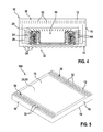
- Figure 4 illustrates a combined side view (in the lower part of the Figure) and top view (in the upper part of the Figure) of the example embodiment of Figure 2 showing in detail the compactness of the arrangement.
- the contacts 32 of the test portal 30 are easily accessible on the top surface 12 of the carrier.
- Figure 5 displays an example embodiment of a semiconductor package 100 comprising a carrier 10 according to the invention.
- the component 50 is covered by a seal 50, for instance a mold molded over the recess 22.
- the contacts 32 of the test portal 30 are still fully accessible after overmolding the component 50.
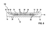
- Figure 6 shows in a side cut view the semiconductor package 100 of Figure 5 .
- the component 50 arranged on the seat 20 in the recess 22 comprises three stacked semiconductor dies 52 separated by spacers 54.
- the semiconductor package 100 is assembled by mounting the BGA internals such as semiconductor die 52, passive components (not shown) and the like within the recess 22 formed by the multi-layered printed circuit board (PCB) assembly (carrier 10). Both the top and bottom surfaces 12, 14 of the carrier 10 have metalized pads (contacts 32, 34), with one side (bottom surface 14) being bumped for surface mount technology (SMT) assembly with solder spheres 34.
- PCB routing with routing paths 38 ( Figures 7 , 8 ) allow interconnections between the BGA internals and either surface 12, 14, as well as between top and bottom surfaces 12, 14.
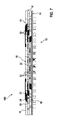
- FIGS 7 and 8 depict in different views the metallic interconnects or routing paths 38 which are arranged to provide interconnections between the component 50 mounted to the seat 20 and the top and bottom surfaces 12, 14 as well as between the bottom terminal region 36 and the contacts 32 of the test portal 30.
- the routing paths 38 are arranged in the carrier 10, particularly in the bottom as well as the side walls 16.
- Figure 9 illustrates an example embodiment of a semiconductor package 100 in form of a header/socket device, wherein a header 110 cooperates with a socket which provides the test portal 30.
- the header 110 has a multitude of pins 132 at the interface facing the contacts 32 of the test portal 30 so that the pins 132 can establish an electrical contact between the pins 132 and the contacts 32 of the test portal 30.
Landscapes
- Testing Of Individual Semiconductor Devices (AREA)
- Physics & Mathematics (AREA)
- Geometry (AREA)
Abstract
Description
- The invention relates to a semiconductor device and more specifically, to a semiconductor package.
- It is known in the art to provide test points on hybrid electronics modules. All test points must be routed to metalized points in one of the module surfaces which results in a routing effort as well as a high space requirement.
- It is an object of the invention to provide a carrier for a semiconductor package with reduced space requirements for routing test points to the semiconductor module.
- It is a further object of the invention to provide a semiconductor package with reduced space requirements for routing test points to the semiconductor module.
- The objects are achieved by the features of the independent claims. The other claims, the description and the drawing include favourable embodiments of the invention.
- According a first aspect of the invention, a carrier for a semiconductor package is proposed, having a top surface and a bottom surface separated by side walls, comprising a seat for a component and at least one terminal region for electrically connecting the component to the carrier when mounted to the seat, wherein a test portal is arranged at an outer surface of the carrier, and wherein one or more routing paths are arranged in the carrier for routing one or more electrical contacts arranged at the carrier to the test portal.
- It is of advantage that the invention allows for a standardized test point methodology. Module-level test systems for both engineering and production uses can be designed for a simplified header/socket model with minimal tooling change between testing different models.
- Expediently, the test portal comprises a multitude of test points which can be accessed from outside the carrier and, after assembly of the semiconductor package, from outside the semiconductor package. Advantageously, a standardized test-point solution is made available that reduces board-level routing and space requirements, which retains accessibility of the test points through the assembly process.
- The invention is particularly useful for hybrid electronics modules, such as semiconductor modules. Typically a semiconductor package is one of many components placed on the hybrid electronics module. The invention allows for reducing or eliminating the test points that have to be routed to the electronics module by incorporating the test portal on the semiconductor package.
- According to an advantageous embodiment, an outer terminal region may be arranged at the bottom surface comprising first contacts. The carrier can be used for surface mount technology (SMT). Particularly, one or more first electrical contacts may be arranged in the outer terminal region, wherein at least one first contact may be routed through the carrier to the test portal. More particularly, the outer terminal region may comprise a termination grid array, particularly one of a ball-grid array (BGA), pin-grid array (PGA), column-grid array (CGA), or land-grid array (LGA). Advantageously, the number of the electrical contacts in the grid array solder spheres in the grid ball array can be increased as needed to route test points originating externally from the outer terminal region to the test portal.
- According to an advantageous embodiment, the routing paths may be arranged to provide interconnections between the component (when mounted to the seat) and the top and bottom surfaces as well as between the bottom terminal region and the test portal. A standardized design can be provided for SMT packages.
- According to an advantageous embodiment, the test portal may be arranged at the an external surface, e.g. at the top surface and/or at one or more side walls. The contacts of the test portal can be easily accessed.
- According to an advantageous embodiment, the seat may be arranged in a recess surrounded by the side walls. This allows for sealing the seat when the component is mounted to the carrier, while the test portal can be arranged outside the recess. Optionally, instead of providing a recess in the side walls a selective/partial overmolding of the component can be used as well.
- According to an advantageous embodiment, the seat may be arranged to accommodate an electric component comprising two or more electric circuit layers, wherein each layer may be connectable separately to the terminal region. A compact design is possible with high density and complex devices.
- According to an advantageous embodiment, the seat may be arranged in a tiered terminal region. Establishing the electrical connections of multi-layered circuit boards in the recess is facilitated. The tiered structure is optional, as in more basic cases only a single semiconductor component may be included.
- According to another aspect of the invention, a semiconductor package is proposed comprising a carrier and an electric component, the carrier having a top surface and a bottom surface separated by side walls, comprising a seat for a component and at least one terminal region for electrically connecting the component to the carrier when mounted to the seat, wherein a test portal is arranged at an outer surface of the carrier, and wherein one or more routing paths are arranged in the carrier for routing one or more electrical contacts arranged at the carrier to the test portal.
- It is of advantage that the overall size of the end-use electronic module can shrink as surface real-estate for test points in the test portal and associated multi-level routing in the electric component can be reduced or eliminated. With a header/socket, the test point density can also be increased. Test points can be aligned on a specific grid pattern so that a "universal" socket could be used for multiple different semiconductor packages.
- According to an advantageous embodiment, an outer terminal region may be arranged at the bottom surface comprising first contacts, favourably one or more first electrical contacts are arranged in the outer terminal region and wherein at least one first contact is routed through the carrier to the test portal. While one or more connections from the outer terminal connection to the test portal may be implemented, this is not an absolute requirement. i.e., there could be embodiments where the test portal is only used to enhance test coverage of the component within the semiconductor package but not of the hybrid module.
- According to an advantageous embodiment, the routing paths may be arranged to provide interconnections between the component when mounted to the seat and the top and bottom surfaces as well as between the bottom terminal region and the test portal.
- According to an advantageous embodiment, the test portal may be arranged at an external surface, e.g. at the top surface and/or at side walls, thus providing easy accessibility for both for both engineering and production uses. Routing for top-side test points also facilitates the addition of additional electronic components such as decoupling caps on top of or within the BGA package. A decoupling cap is a specific type of small electronic component. However, any electronic component small enough to be mounted within or on top of the package could be used.
- According to an advantageous embodiment, the seat may be arranged to accommodate an electric component, which is sealed by a seal to protect the electric component in the carrier, and wherein the seal is arranged in an inner portion of the semiconductor package and the test portal is arranged in an outer portion of the semiconductor package.
- Favourably, the invention provides a termination-grid-array package with top-side accessible test points. Test points may address nodes originating from the contents of the package (i.e., semiconductor die) as well as test points originating from an electronic circuit (module) on which the package is mounted.
- The present invention together with the above-mentioned and other objects and advantages may best be understood from the following detailed description of the embodiments, but not restricted to the embodiments, wherein is shown in:
- Fig. 1
- an example embodiment of a carrier according to the invention;
- Fig. 2a
- a component wire bonded to the carrier of
Fig. 1 with a test portal at the top surface; - Fig. 2b
- a component wire bonded to the carrier of
Fig. 1 with a test portal at the top surface and the side walls; - Fig. 3
- in a bottom view the carrier of
Fig. 1 ; - Fig. 4
- a combined side and top view of the example embodiment of
Fig. 2a ; - Fig. 5
- an example embodiment of a semiconductor package comprising a carrier according to the invention;
- Fig. 6
- a side cut view the semiconductor package of
Fig. 5 ; - Fig. 7
- in a side view routing paths of an example embodiment of a carrier with a component wire bonded to the carrier according to the invention;
- Fig. 8
- a perspective, partially cut open top view of routing paths of the carrier of
Fig. 7 ; - Fig. 9
- a perspective, exploded view of a header/socket device.
- In the drawings, like elements are referred to with equal reference numerals. The drawings are merely schematic representations, not intended to portray specific parameters of the invention. Moreover, the drawings are intended to depict only typical embodiments of the invention and therefore should not be considered as limiting the scope of the invention.
-
Figure 1 depicts an example embodiment of acarrier 10 according to the invention. Thecarrier 10 has atop surface 12 and abottom surface 14 separated byside walls 16. Thecarrier 10 is advantageously embodied as a multi-layered printed circuit board assembly comprising aseat 20 for mounting anelectric component 50 such as a semiconductor die. - A first and a second
terminal region component 50 to thecarrier 10 are arranged in arecess 22 which includes theseat 20. Theterminal regions seat 20 to theupper surface 12. - A
test portal 30 is arranged at outer surfaces of thecarrier 10, e.g. at thetop surface 12 and atside walls 16. Multiple routing paths (38 inFigures 7 and8 are arranged in thecarrier 10 for routing one or more electrical contacts arranged at thecarrier 10 to thetest portal 30. Thetest portal 30 is arranged on thetop surface 12 of thecarrier 10 on two sides of therecess 22 and comprises a multitude ofcontacts 32, for instance metal plated pads. -
Figure 2a depicts acomponent 50 wire bonded withwires 60 to the carrier ofFigure 1 . Thetest portal 30 is arranged at two opposing sides of thetop surface 12.Figure 2b shows an arrangement where thetest portal 30 is arranged at two opposing sides of thetop surface 12 and at allside walls 16. Thecomponent 50 may for instance comprise three semiconductor dies 52 which are wire bonded to the respective terminals in theterminal regions recess 22. -
Figure 3 shows in a bottom view the carrier ofFigure 1 , displaying an outerterminal region 36 arranged at thebottom surface 14 of thecarrier 10. The outerterminal region 36 comprises firstelectrical contacts 34 wherein one or morefirst contact 34 are routed through thecarrier 10 to thecontacts 32 of thetest portal 30. The outerterminal region 36 can be embodied as a termination-grid array, by way of example as a ball grid array. A ball grid array (BGA) is a package of an integrated circuit with the bottom of the package covered or partly covered with solder balls or spheres in a grid pattern. The solder spheres conduct electrical signals from the integrated circuit of a printed circuit board (PCB). These solder spheres can be placed manually or with automated equipment and are held in place with a flux until soldering occurs. The device is placed on a PCB with terminal pads in a pattern that matches the array of solder spheres. The assembly is then heated, e.g. in a reflow oven or by an infrared heater, causing the solder spheres to melt. Surface tension causes the molten solder to hold the package in alignment with the PCB, at the correct separation distance, while the solder cools and solidifies. - The BGA allows for surface mount technology assembly of the
carrier 10. The top-side space of the BGA package is used as astandardized test portal 30 for both the component-level and end-use electronic module. An existing BGA bump I/O count (i.e. the number of the solder spheres 34) may be expanded as needed to route test points originating externally from the BGA to thetop side 12 of the package. -
Figure 4 illustrates a combined side view (in the lower part of the Figure) and top view (in the upper part of the Figure) of the example embodiment ofFigure 2 showing in detail the compactness of the arrangement. Thecontacts 32 of thetest portal 30 are easily accessible on thetop surface 12 of the carrier. -
Figure 5 displays an example embodiment of asemiconductor package 100 comprising acarrier 10 according to the invention. Thecomponent 50 is covered by aseal 50, for instance a mold molded over therecess 22. Thecontacts 32 of thetest portal 30 are still fully accessible after overmolding thecomponent 50. -
Figure 6 shows in a side cut view thesemiconductor package 100 ofFigure 5 . Thecomponent 50 arranged on theseat 20 in therecess 22 comprises three stacked semiconductor dies 52 separated byspacers 54. - The
semiconductor package 100 is assembled by mounting the BGA internals such as semiconductor die 52, passive components (not shown) and the like within therecess 22 formed by the multi-layered printed circuit board (PCB) assembly (carrier 10). Both the top andbottom surfaces carrier 10 have metalized pads (contacts 32, 34), with one side (bottom surface 14) being bumped for surface mount technology (SMT) assembly withsolder spheres 34. PCB routing with routing paths 38 (Figures 7 ,8 ) allow interconnections between the BGA internals and eithersurface bottom surfaces -
Figures 7 and8 depict in different views the metallic interconnects orrouting paths 38 which are arranged to provide interconnections between thecomponent 50 mounted to theseat 20 and the top andbottom surfaces terminal region 36 and thecontacts 32 of thetest portal 30. Therouting paths 38 are arranged in thecarrier 10, particularly in the bottom as well as theside walls 16. -
Figure 9 illustrates an example embodiment of asemiconductor package 100 in form of a header/socket device, wherein aheader 110 cooperates with a socket which provides thetest portal 30. Theheader 110 has a multitude ofpins 132 at the interface facing thecontacts 32 of thetest portal 30 so that thepins 132 can establish an electrical contact between thepins 132 and thecontacts 32 of thetest portal 30.
Claims (16)
- A carrier (10) for a semiconductor package (100), having a top surface (12) and a bottom surface (14) separated by side walls (16), comprising a seat (20) for a component (50) and at least one terminal region (24, 26) for electrically connecting the component (50) to the carrier (10) when mounted to the seat (20), wherein a test portal (30) is arranged at an outer surface of the carrier (10), and wherein one or more routing paths (38) are arranged in the carrier (10) for routing one or more electrical contacts arranged at the carrier (10) to the test portal (30).
- The carrier according to claim 1, wherein an outer terminal region (36) is arranged at the bottom surface (14) comprising first contacts (34).
- The carrier according to claim 1, wherein the outer terminal region (36) comprises a termination-grid array, particularly at least one of a ball-grid array (BGA), pin-grid array (PGA), column-grid array (CGA), or land-grid array.
- The carrier according to claim 3, wherein one or more first electrical contacts (34) are arranged in the outer terminal region (36).
- The carrier according to claim 4, wherein at least one first contact (34) is routed through the carrier (10) to the test portal (30).
- The carrier according to claim 1, wherein the routing paths (38) are arranged to provide interconnections between the component (50) when mounted to the seat (20) and the top and bottom surfaces (12, 14) as well as between the bottom terminal region (36) and the test portal (30).
- The carrier according to claim 1, wherein the test portal (30) is arranged at an external surface (12, 16).
- The carrier according to claim 1, wherein the seat (20) is arranged in a recess (22) surrounded by the side walls (16).
- The carrier according to claim 1, wherein the seat (20) is arranged to accommodate an electric component (50) comprising two or more electric circuit layers (52), wherein each layer (52) is connectable separately to the terminal region (24, 26).
- The carrier according to claim 1, wherein the seat (20) is arranged in a tiered terminal region (24, 26).
- A semiconductor package (100) comprising a carrier (10), the carrier (10) having a top surface (12) and a bottom surface (14) separated by side walls (16), comprising a seat (20) for a component (50) and at least one terminal region (24, 26) for electrically connecting the component (50) to the carrier (10) when mounted to the seat (20), wherein a test portal (30) is arranged at an outer surface of the carrier (10), and wherein one or more routing paths (38) are arranged in the carrier (10) for routing one or more electrical contacts arranged at the carrier (10) to the test portal (30).
- The semiconductor package according to claim 11, wherein an outer terminal region (36) is arranged at the bottom surface (14) comprising first contacts (34).
- The semiconductor package according to claim 12, wherein one or more first electrical contacts (34) are arranged in the outer terminal region (36) and wherein at least one first contact (34) is routed through the carrier (10) to the test portal (30).
- The semiconductor package according to claim 11, wherein the routing paths (38) are arranged to provide interconnections between the component (50) when mounted to the seat (20) and the top and bottom surfaces (12, 14) as well as between the bottom terminal region (36) and the test portal (30).
- The semiconductor package according to claim 11, wherein the test portal (30) is arranged at an external surface (12, 16).
- The semiconductor package according to claim 11, wherein the seat (20) is arranged to accommodate an electric component (50), which is sealed by a seal (70) to protect the electric component (50) in the carrier (10), and wherein the seal (70) is arranged in an inner portion of the semiconductor package (100) and the test portal (30) is arranged in an outer portion of the semiconductor package (100).
Applications Claiming Priority (1)
| Application Number | Priority Date | Filing Date | Title |
|---|---|---|---|
| US201161497966P | 2011-06-17 | 2011-06-17 |
Publications (2)
| Publication Number | Publication Date |
|---|---|
| EP2535926A2 true EP2535926A2 (en) | 2012-12-19 |
| EP2535926A3 EP2535926A3 (en) | 2015-08-05 |
Family
ID=46087515
Family Applications (1)
| Application Number | Title | Priority Date | Filing Date |
|---|---|---|---|
| EP12167254.7A Withdrawn EP2535926A3 (en) | 2011-06-17 | 2012-05-09 | Semiconductor package |
Country Status (3)
| Country | Link |
|---|---|
| US (1) | US8981546B2 (en) |
| EP (1) | EP2535926A3 (en) |
| JP (1) | JP2013004984A (en) |
Cited By (1)
| Publication number | Priority date | Publication date | Assignee | Title |
|---|---|---|---|---|
| WO2022090731A1 (en) * | 2020-10-30 | 2022-05-05 | Npl Management Limited | Ion microtrap assembly and method of making of making such an assembly |
Families Citing this family (3)
| Publication number | Priority date | Publication date | Assignee | Title |
|---|---|---|---|---|
| CN104966708B (en) | 2015-07-01 | 2018-06-12 | 英特尔公司 | Semiconductor Package Structure |
| US10916529B2 (en) * | 2018-03-29 | 2021-02-09 | Taiwan Semiconductor Manufacturing Company, Ltd. | Electronics card including multi-chip module |
| EP3603740A1 (en) * | 2018-08-02 | 2020-02-05 | BIOTRONIK SE & Co. KG | Implant |
Family Cites Families (11)
| Publication number | Priority date | Publication date | Assignee | Title |
|---|---|---|---|---|
| JPH05102262A (en) * | 1991-10-03 | 1993-04-23 | Hitachi Ltd | Semiconductor device and mounting device mounting the same |
| US5334857A (en) * | 1992-04-06 | 1994-08-02 | Motorola, Inc. | Semiconductor device with test-only contacts and method for making the same |
| JP3150560B2 (en) * | 1995-03-07 | 2001-03-26 | 松下電子工業株式会社 | Semiconductor device |
| JP3447908B2 (en) * | 1997-02-13 | 2003-09-16 | 富士通株式会社 | Ball grid array package |
| JP3052874B2 (en) * | 1997-02-19 | 2000-06-19 | 日本電気株式会社 | Probe device for BGA type semiconductor device |
| JPH1117058A (en) * | 1997-06-26 | 1999-01-22 | Nec Corp | BGA package, its test socket, and method of testing BGA package |
| US20040135242A1 (en) * | 2003-01-09 | 2004-07-15 | Hsin Chung Hsien | Stacked structure of chips |
| US7100814B2 (en) * | 2004-02-18 | 2006-09-05 | Cardiac Pacemakers, Inc. | Method for preparing integrated circuit modules for attachment to printed circuit substrates |
| JP4322844B2 (en) * | 2005-06-10 | 2009-09-02 | シャープ株式会社 | Semiconductor device and stacked semiconductor device |
| EP2071680A4 (en) * | 2006-09-19 | 2012-11-07 | Panasonic Corp | SOCKET, MODULE CARD AND INSPECTION SYSTEM USING THE MODULE CARD |
| JP2008277595A (en) * | 2007-05-01 | 2008-11-13 | Matsushita Electric Ind Co Ltd | Semiconductor device and manufacturing method thereof |
-
2012
- 2012-05-09 EP EP12167254.7A patent/EP2535926A3/en not_active Withdrawn
- 2012-05-29 US US13/482,511 patent/US8981546B2/en active Active
- 2012-06-15 JP JP2012135669A patent/JP2013004984A/en active Pending
Non-Patent Citations (1)
| Title |
|---|
| None |
Cited By (2)
| Publication number | Priority date | Publication date | Assignee | Title |
|---|---|---|---|---|
| WO2022090731A1 (en) * | 2020-10-30 | 2022-05-05 | Npl Management Limited | Ion microtrap assembly and method of making of making such an assembly |
| US12588526B2 (en) | 2020-10-30 | 2026-03-24 | Npl Management Limited | Ion microtrap assembly and method of making of making such an assembly |
Also Published As
| Publication number | Publication date |
|---|---|
| EP2535926A3 (en) | 2015-08-05 |
| US8981546B2 (en) | 2015-03-17 |
| JP2013004984A (en) | 2013-01-07 |
| US20120319288A1 (en) | 2012-12-20 |
Similar Documents
| Publication | Publication Date | Title |
|---|---|---|
| US20220117087A1 (en) | Stackable via package and method | |
| US5767580A (en) | Systems having shaped, self-aligning micro-bump structures | |
| KR100884172B1 (en) | Integrated circuit package stack and integrated circuit package formed by | |
| US8888504B2 (en) | Multilevel interconnection system | |
| CN113130435A (en) | Package structure and method for manufacturing the same | |
| US20100270667A1 (en) | Semiconductor package with multiple chips and substrate in metal cap | |
| US10707156B2 (en) | Electronic device | |
| US20100170706A1 (en) | Electronic module and method for manufacturing an electronic module | |
| US20110147908A1 (en) | Module for Use in a Multi Package Assembly and a Method of Making the Module and the Multi Package Assembly | |
| US8981546B2 (en) | Semiconductor package | |
| US20140353824A1 (en) | Package-on-package structure | |
| KR20080055642A (en) | Laminated package and its manufacturing method | |
| CN119731786A (en) | Power module package with molded through-hole and double-sided crimp pins | |
| EP2883430B1 (en) | A printed circuit board arrangement and a method for forming electrical connection at a printed circuit board | |
| KR101831680B1 (en) | Integrated device package, wire-to-die connector, and apparatus related thereto | |
| US8097950B2 (en) | Semiconductor device and electronic component module using the same | |
| US10653020B2 (en) | Electronic module and method for producing an electronic module | |
| CN105742274B (en) | Chip package vertical transition connector, board structure and production method | |
| US20220278089A1 (en) | Semiconductor package structure and packaging method thereof | |
| US20170133305A1 (en) | 3d system-level packaging methods and structures | |
| CN105957837A (en) | Packaging structure used for three-dimensional system level packaging and packaging method | |
| CN113972069B (en) | Method for manufacturing resin molded electronic component, and resin molded electronic component | |
| US10236270B2 (en) | Interposer and semiconductor module for use in automotive applications | |
| EP2996145B1 (en) | Inter-connection of a lead frame with a passive component intermediate structure | |
| JP4459421B2 (en) | Semiconductor device |
Legal Events
| Date | Code | Title | Description |
|---|---|---|---|
| PUAI | Public reference made under article 153(3) epc to a published international application that has entered the european phase |
Free format text: ORIGINAL CODE: 0009012 |
|
| AK | Designated contracting states |
Kind code of ref document: A2 Designated state(s): AL AT BE BG CH CY CZ DE DK EE ES FI FR GB GR HR HU IE IS IT LI LT LU LV MC MK MT NL NO PL PT RO RS SE SI SK SM TR |
|
| AX | Request for extension of the european patent |
Extension state: BA ME |
|
| PUAL | Search report despatched |
Free format text: ORIGINAL CODE: 0009013 |
|
| AK | Designated contracting states |
Kind code of ref document: A3 Designated state(s): AL AT BE BG CH CY CZ DE DK EE ES FI FR GB GR HR HU IE IS IT LI LT LU LV MC MK MT NL NO PL PT RO RS SE SI SK SM TR |
|
| AX | Request for extension of the european patent |
Extension state: BA ME |
|
| RIC1 | Information provided on ipc code assigned before grant |
Ipc: H01L 23/13 20060101AFI20150629BHEP Ipc: H01L 23/498 20060101ALI20150629BHEP |
|
| STAA | Information on the status of an ep patent application or granted ep patent |
Free format text: STATUS: THE APPLICATION IS DEEMED TO BE WITHDRAWN |
|
| 18D | Application deemed to be withdrawn |
Effective date: 20160206 |