EP2535904B1 - Ceramic heater, and manufacturing method thereof - Google Patents
Ceramic heater, and manufacturing method thereof Download PDFInfo
- Publication number
- EP2535904B1 EP2535904B1 EP12004535.6A EP12004535A EP2535904B1 EP 2535904 B1 EP2535904 B1 EP 2535904B1 EP 12004535 A EP12004535 A EP 12004535A EP 2535904 B1 EP2535904 B1 EP 2535904B1
- Authority
- EP
- European Patent Office
- Prior art keywords
- foam metal
- metal member
- electrode
- ceramic heater
- ceramic
- Prior art date
- Legal status (The legal status is an assumption and is not a legal conclusion. Google has not performed a legal analysis and makes no representation as to the accuracy of the status listed.)
- Not-in-force
Links
Images
Classifications
-
- H—ELECTRICITY
- H01—ELECTRIC ELEMENTS
- H01C—RESISTORS
- H01C1/00—Details
- H01C1/14—Terminals or tapping points specially adapted for resistors; Arrangements of terminals or tapping points on resistors
-
- H—ELECTRICITY
- H05—ELECTRIC TECHNIQUES NOT OTHERWISE PROVIDED FOR
- H05B—ELECTRIC HEATING; ELECTRIC LIGHT SOURCES NOT OTHERWISE PROVIDED FOR; CIRCUIT ARRANGEMENTS FOR ELECTRIC LIGHT SOURCES, IN GENERAL
- H05B3/00—Ohmic-resistance heating
- H05B3/02—Details
- H05B3/06—Heater elements structurally combined with coupling elements or holders
- H05B3/08—Heater elements structurally combined with coupling elements or holders having electric connections specially adapted for high temperatures
-
- H—ELECTRICITY
- H05—ELECTRIC TECHNIQUES NOT OTHERWISE PROVIDED FOR
- H05B—ELECTRIC HEATING; ELECTRIC LIGHT SOURCES NOT OTHERWISE PROVIDED FOR; CIRCUIT ARRANGEMENTS FOR ELECTRIC LIGHT SOURCES, IN GENERAL
- H05B3/00—Ohmic-resistance heating
- H05B3/10—Heating elements characterised by the composition or nature of the materials or by the arrangement of the conductor
- H05B3/12—Heating elements characterised by the composition or nature of the materials or by the arrangement of the conductor characterised by the composition or nature of the conductive material
- H05B3/14—Heating elements characterised by the composition or nature of the materials or by the arrangement of the conductor characterised by the composition or nature of the conductive material the material being non-metallic
- H05B3/141—Conductive ceramics, e.g. metal oxides, metal carbides, barium titanate, ferrites, zirconia, vitrous compounds
-
- H—ELECTRICITY
- H05—ELECTRIC TECHNIQUES NOT OTHERWISE PROVIDED FOR
- H05B—ELECTRIC HEATING; ELECTRIC LIGHT SOURCES NOT OTHERWISE PROVIDED FOR; CIRCUIT ARRANGEMENTS FOR ELECTRIC LIGHT SOURCES, IN GENERAL
- H05B2203/00—Aspects relating to Ohmic resistive heating covered by group H05B3/00
- H05B2203/022—Heaters specially adapted for heating gaseous material
- H05B2203/024—Heaters using beehive flow through structures
-
- Y—GENERAL TAGGING OF NEW TECHNOLOGICAL DEVELOPMENTS; GENERAL TAGGING OF CROSS-SECTIONAL TECHNOLOGIES SPANNING OVER SEVERAL SECTIONS OF THE IPC; TECHNICAL SUBJECTS COVERED BY FORMER USPC CROSS-REFERENCE ART COLLECTIONS [XRACs] AND DIGESTS
- Y10—TECHNICAL SUBJECTS COVERED BY FORMER USPC
- Y10T—TECHNICAL SUBJECTS COVERED BY FORMER US CLASSIFICATION
- Y10T29/00—Metal working
- Y10T29/49—Method of mechanical manufacture
- Y10T29/49002—Electrical device making
- Y10T29/49082—Resistor making
- Y10T29/49083—Heater type
Definitions
- the present invention relates to a ceramic heater provided with a ceramic resistor which is a resistor made of ceramic.
- Japanese Unexamined Patent Application Publication No. 9.106883 discloses a ceramic heater which is manufactured as follows. That is, main materials, of the ceramic heater, such as silicon carbide and metallic silicon are first mixed together, added with water, and then kneaded; the resulting mixture is extruded and molded in a honeycomb structure; the molded main materials are sintered, resulting in forming a ceramic resistor.
- An electrode is formed by applying silver paste having electrical conductivity on a surface of the ceramic resistor and then sintering such a ceramic resistor, or by performing thermal-spraying of pure aluminum onto a surface of the ceramic resistor.
- the electrode formed as above is pressed by a plate-like electrode presser. An electric wire is connected to the electrode presser.
- the following case may occur: due to small concaves and convexes, or wavy swells in the surface of the ceramic resistor on which the electrode is formed, a surface of the electrode is not flat. In this case, even if the electrode presser is pressed against the electrode, electric resistance may be biased depending on portions of the ceramic heater. As a result, a problem may arise in which temperature-rise performance of the ceramic heater is biased depending on the portions of the ceramic heater.
- a ceramic heater according to a first aspect of the present invention includes a ceramic resistor, at least one metallic film, and at least one foam metal member.
- the at least one metallic film is formed on at least one surface of the ceramic resistor.
- the at least one surface is assigned as at least one electrode plane.
- the at least one foam metal member is formed in a plate-like shape.
- the at least one foam metal member covers and is attached to the at least one metallic film.
- At least one electrode is attached to the at least one foam metal member and has a contact area with the at least one foam metal member smaller than an apparent area of the at least one foam metal member, the apparent area being an entire area of one surface of the at least one foam metal member.
- the at least one foam metal member is deformed corresponding to the concaves and convexes or the swells in the at least one electrode plane. For this reason, the at least one metallic film and the at least one foam metal member are attached to each other without forming gaps therebetween. Thus, it is possible to inhibit differences in electric resistance, and therefore, inhibit bias in temperature-rise performance depending on portions of the ceramic heater.
- the contact area between the at least one foam metal member and the at least one electrode is small, electric current can be distributed throughout the entire the ceramic resistor via the at least one foam metal member. Consequently, it is possible to cause the entire ceramic heater to generate heat in a substantially uniform manner. Thus, differences in temperature-rise performance can be suppressed.
- the at least one metallic film may be formed in any manners.
- the at least one metallic film may be formed over an entire area of the at least one electrode plane.
- the at least one foam metal member may cover and be attached over an entire area of the at least one metallic film.
- the at least one foam metal member may be attached to the at least one metallic film by diffusion-bonding.
- the diffusion-bonding allows more ensured attachment between the at least one foam metal member and the at least one metallic film without forming gaps therebetween.
- the at least one foam metal member may be metallically bonded to the at least one metallic film.
- the respective contact surfaces of the at least one foam metal member and the at least one metallic film are inhibited from directly contacting with an outer environment, thereby inhibiting increase of electric resistance over time.
- the at least one electrode may be attached to the at least one foam metal member in any manners.
- the at least one electrode may be attached to a generally central region of a surface of the at least one foam metal member so as to stand from the at least one foam metal member in a generally vertical direction.
- the ceramic resistor may have any shape.
- the ceramic resistor may be hexahedron shaped.
- the at least one metallic film may be two metallic films formed on a pair of opposing surfaces of the ceramic resistor.
- the at least one foam metal member may be two foam metal members attached respectively to the two metallic films.
- the at least one electrode may be two electrodes attached respectively to the two foam metal members.
- the at least one electrode may be attached to the at least one foam metal member by diffusion-bonding.
- the diffusion-bonding allows more ensured attachment between the at least one electrode and the at least one foam metal member without forming gaps therebetween.
- the at least one electrode may be metallically bonded to the at least one foam metal member.
- the respective contact surfaces of the at least one electrode and the at least one foam metal member are inhibited from directly contacting with an outer environment, thereby inhibiting increase of electric resistance over time.
- the ceramic resistor may have any shape, and for example, may have a honeycomb shape.
- the ceramic resistor formed in a honeycomb shape allows a fluid to flow through inside the ceramic resistor and thus, to increase a temperature of the fluid flowing through thereinside.
- a method for manufacturing a ceramic heater according to a second aspect of the present invention comprises the step of forming at least one metallic film on at least one surface of a ceramic resistor.
- the method further comprises the steps of: placing and attaching at least one foam metal member, which is formed in a plate-like shape, over the at least one metallic film; and attaching at least one electrode to the at least one foam metal member; the at least one electrode having a contact area with the at least one foam metal member smaller than an apparent area of the at least one foam metal member, and the apparent area being an entire area of one surface of the at least one foam metal member.
- the ceramic heater in the first aspect it is possible to manufacture the ceramic heater in the first aspect, and therefore, provide a ceramic heater in which temperature-rise performance is inhibited from being biased depending on portions of the ceramic heater
- a ceramic heater 1 is housed inside a duct 2.
- a fluid which is to be flowed through inside the duct 2 is air.
- the fluid is not limited to air, and may be a gas other than air or may be a liquid such as water, etc.
- the ceramic heater 1 includes a ceramic resistor 4 having a generally honeycomb structure. More specifically, the ceramic resistor 4 of the present embodiment is divided by a plurality of longitudinal ribs and a plurality of lateral ribs in a grid-like manner, so that a plurality of rectangular through holes 6 are formed in the ceramic resistor 4.
- the ceramic resistor 4 constituted as above is formed as follows: main materials such as silicon carbide and metallic silicon are first mixed together, added with water, and then kneaded; the resulting mixture is extruded and molded into a honeycomb structure; the molded main materials in honeycomb structure are reacted and sintered in a furnace under a nitrogen (inert gas) atmosphere; and as a result, the ceramic resistor 4, which is a composite of silicon carbide and silicon nitride, is formed.
- the ceramic resistor 4 has electrical conductivity, and is porous as explained above.
- the ceramic resistor 4 has an appearance of a cuboid shaped hexahedron.
- the through holes 6 have openings at end surfaces 4a and 4b of the ceramic resistor 4.
- the through holes 6 penetrate through the ceramic resistor 4 in a longitudinal direction of the ceramic resistor 4.
- Four surfaces of the ceramic resistor 4, which do not include the end surfaces 4a and 4b, are flat without a through hole.
- Electrode plane two opposing surfaces are assigned as a plane for an electrode (hereinafter referred to as "electrode plane”).
- Metallic films 8a and 8b are formed respectively on these two electrode planes.
- the metallic films 8a and 8b are formed over entire areas of the electrode planes.
- the metallic films 8a and 8b as such may be formed by applying silver paste having heat-resistance and electrical conductivity on the electrode planes and thereafter sintering the ceramic resistor 4 at a high temperature.
- the metallic films 8a and 8b may be formed by performing thermal-spraying of pure aluminum onto the electrode planes.
- Plate-like foam metal members 10 and 12 cover and are attached to the metallic films 8a and 8b, respectively.
- the foam metal members 10 and 12 are formed respectively in sizes sufficient to cover entire surfaces of the respective metallic films 8a and 8b.
- the foam metal members 10 and 12 are formed as below. Firstly, metallic powder, water-soluble binder, surfactant, and water are mixed together. Then, a non-water soluble organic solvent is further added to and mixed with the resulting mixture. Consequently, a compact in which all of the mixed materials are evenly dispersed and distributed is formed. By holding this compact at a constant temperature, the non-water soluble organic solvent contained in the compact is gasified and evaporated as a gas.
- the foam metal members 10 and 12 formed as above are sintered at a high temperature so as to sinter portions consisting of the metallic powders. Consequently, such sintered foam metal members 10 and 12 become a porous metal body having electrical conductivity.
- the porous metal body is composed of framework structures which enclose air pores formed by the air bubbles.
- a material of the metallic powders it is preferable to use a material having an excellent electrical conductivity, such as copper-based or aluminum-based materials.
- a diameter of the air pores in the foam metal members 10 and 12 and a porosity of the foam metal members 10 and 12 may be preferably determined by experiments, etc.
- the foam metal members 10 and 12 are attached, respectively, to the metallic films 8a and 8b by diffusion-bonding where the metallic films 8a and 8b and the foam metal members 10 and 12 are heated while being pressed against each other.
- the diffusion bonding causes interdiffusion between these metals which are in contact with each other.
- the ceramic resistor 4 can be diffusion-bonded to the foam metal members 10 and 12, respectively, via the metallic films 8a and 8b. Moreover, since there may be small concaves and convexes, or small wavy swells in the electrode planes of the ceramic resistor 4, these electrode planes may be coarse or have a low flatness.
- the foam metal members 10 and 12 can be closely attached, respectively, to the metallic films 8a and 8b without forming gaps therebetween. This is because, at the time when the foam metal members 10 and 12 are diffusion-bonded to the respective metallic films 8a and 8b, the foam metal members 10 and 12 are deformed corresponding to the concaves and convexes or the swells in the electrode planes.
- the small convexes in the electrode planes are entered into the air pores formed in attachment surfaces of the foam metal members 10 and 12.
- the small convexes are pressed into the attachment surfaces of the foam metal members 10 and 12.
- the concaves and convexes in the electrode planes are absorbed, and thus, entire surfaces of the foam metal members 10 and 12 are closely attached to the metallic films 8a and 8b, respectively.
- the foam metal members 10 and 12 are deformed along the swell.
- the entire surfaces of the foam metal members 10 and 12 are closely attached to the metallic films 8a and 8b, respectively.
- a metal electrode 14 is attached to a generally central region of a surface of the plate-like foam metal member 10.
- a metal electrode 16 is attached to a generally central region of a surface of the plate-like foam metal member 12.
- the electrodes 14 and 16 are attached, respectively, to the foam metal members 10 and 12 by diffusion-bonding.
- An attachment area between the electrode 14 and the foam metal member 10 is smaller than an apparent area of the foam metal member 10.
- an attachment area between the electrode 16 and the foam metal member 12 is smaller than an apparent area of the foam metal member 12.
- the electrodes 14 and 16 are provided to stand from the respective surfaces of the foam metal members 10 and 12 in a generally vertical direction,
- the surfaces of the foam metal members 10 and 12 consist of metal portions and air-pore portions. Specifically, in the surfaces of the foam metal members 10 and 12, the metal portions and the air-pore portions are positioned in an alternating manner.
- the apparent area of the foam metal member 10 is an entire area of one surface of the foam metal member 10.
- the one surface of the foam metal member 10 includes both of the metal portions and the air-pore portions, and faces to the electrode 14.
- the apparent area of the foam metal member 12 is an entire area of one surface of the foam metal member 12.
- the one surface of the foam metal member 12 includes both of the metal portions and the air-pore portions, and faces to the electrode 16.
- the above attachment areas are smaller than the respective apparent areas of the foam metal members 10 and 12.
- the above attachment areas are respective regions including both of the metal portions and the air-pore portions of the respective foam metal members 10 and 12.
- An attachment operation of three types of components can be facilitated by the following procedure: firstly, overlaying the foam metal member 10 onto the metallic film 8a formed on the ceramic resistor 4; then, further overlaying the electrode 14 onto the above foam metal member 10; and performing diffusion-bonding to the metallic film 8a, the foam metal member 10, and the electrode 14, at the same time.
- the attachment operation of the metallic film 8b, the foam metal member 12, and the electrode 16 can be facilitated by the same procedure as above.
- a contact surface between the metallic film 8a and the foam metal member 10, and a contact surface between the foam metal member 10 and the electrode 14, are closely attached and metallically bonded to each other.
- a contact surface between the metallic film 8b and the foam metal member 12, and a contact surface between the foam metal member 12 and the electrode 16 are closely attached and metallically bonded to each other.
- the ceramic heater 1 is to be covered by a flexible mat 20 which is not electrically conductive. Specifically, the ceramic heater 1 is covered by the mat 20 such that the end surfaces 4a and 4b of the ceramic resistor 4 are not covered and that the surfaces of the foam metal members 10 and 12 are covered. The electrodes 14 and 16 are projected outward from the mat 20.
- the ceramic heater 1 covered by the mat 20 is housed inside the duct 2.
- Each of the electrodes 14 and 16 is projected outward from the duct 2 and connected to a cable.
- the ceramic resistor 4 When the electrodes 14 and 16 are energized, the ceramic resistor 4 generates heat. Therefore, a fluid flowing through inside the duct 2 is heated by flowing through inside the through holes 6.
- the electrodes 14 and 16 When the electrodes 14 and 16 are energized, electric current flows from the electrodes 14 and 16 to the ceramic resistor 4 through the foam metal members 10 and 12 and then the metallic films 8a and 8b.
- the metallic films 8a and 8b are formed on the opposing electrode planes of the ceramic resistor 4. Therefore, a distance between the metallic films 8a and 8b in an energizing direction is uniform. Consequently, current-carrying can be uniformed.
- a resistance value of the foam metal members 10 and 12 can be sufficiently made lower than a resistance value of the ceramic resistor 4. Therefore, electric current can be distributed throughout an entire area of the ceramic resistor 4 via the foam metal members 10 and 12. Consequently, it is possible to cause the entire ceramic resistor 4 to generate heat in a substantially uniform manner.
- the foam metal members 10 and 12 have a lighter weight than a metal plate having a volume the same as a volume of the foam metal members 10 and 12. Moreover, the electrodes 14 and 16 can be formed in a smaller size. As above, it is possible to reduce a weight of the ceramic heater 1.
- the ceramic heater 1 can be made compact in size, the ceramic heater 1 can be used to warm up a small room such as a vehicle interior and a bathroom, etc. or to warm up a specific spot in an area.
Landscapes
- Engineering & Computer Science (AREA)
- Chemical & Material Sciences (AREA)
- Ceramic Engineering (AREA)
- Microelectronics & Electronic Packaging (AREA)
- Resistance Heating (AREA)
- Pressure Welding/Diffusion-Bonding (AREA)
- Surface Heating Bodies (AREA)
Description
- The present invention relates to a ceramic heater provided with a ceramic resistor which is a resistor made of ceramic.
- Japanese Unexamined Patent Application Publication No.
9.106883 - In the above-explained ceramic heater, the following case may occur: due to small concaves and convexes, or wavy swells in the surface of the ceramic resistor on which the electrode is formed, a surface of the electrode is not flat. In this case, even if the electrode presser is pressed against the electrode, electric resistance may be biased depending on portions of the ceramic heater. As a result, a problem may arise in which temperature-rise performance of the ceramic heater is biased depending on the portions of the ceramic heater.
- In one aspect of the present invention, it is desirable to provide a ceramic heater in which temperature-rise performance is inhibited from being biased depending on the portions of the ceramic heater.
- A ceramic heater according to a first aspect of the present invention includes a ceramic resistor, at least one metallic film, and at least one foam metal member. The at least one metallic film is formed on at least one surface of the ceramic resistor. The at least one surface is assigned as at least one electrode plane. The at least one foam metal member is formed in a plate-like shape. The at least one foam metal member covers and is attached to the at least one metallic film.
- At least one electrode is attached to the at least one foam metal member and has a contact area with the at least one foam metal member smaller than an apparent area of the at least one foam metal member, the apparent area being an entire area of one surface of the at least one foam metal member.
- In the ceramic heater constituted as above, even if there are concaves and convexes, or swells in the at least one electrode plane of the ceramic resistor, the at least one foam metal member is deformed corresponding to the concaves and convexes or the swells in the at least one electrode plane. For this reason, the at least one metallic film and the at least one foam metal member are attached to each other without forming gaps therebetween. Thus, it is possible to inhibit differences in electric resistance, and therefore, inhibit bias in temperature-rise performance depending on portions of the ceramic heater.
- If the contact area between the at least one foam metal member and the at least one electrode is small, electric current can be distributed throughout the entire the ceramic resistor via the at least one foam metal member. Consequently, it is possible to cause the entire ceramic heater to generate heat in a substantially uniform manner. Thus, differences in temperature-rise performance can be suppressed.
- Moreover, the at least one metallic film may be formed in any manners. For example, the at least one metallic film may be formed over an entire area of the at least one electrode plane.
- The at least one foam metal member may cover and be attached over an entire area of the at least one metallic film.
- The at least one foam metal member may be attached to the at least one metallic film by diffusion-bonding. The diffusion-bonding allows more ensured attachment between the at least one foam metal member and the at least one metallic film without forming gaps therebetween.
- Moreover, the at least one foam metal member may be metallically bonded to the at least one metallic film. In this case, the respective contact surfaces of the at least one foam metal member and the at least one metallic film are inhibited from directly contacting with an outer environment, thereby inhibiting increase of electric resistance over time.
- The at least one electrode may be attached to the at least one foam metal member in any manners. For example, the at least one electrode may be attached to a generally central region of a surface of the at least one foam metal member so as to stand from the at least one foam metal member in a generally vertical direction.
- Moreover, the ceramic resistor may have any shape. For example, the ceramic resistor may be hexahedron shaped. In this case, the at least one metallic film may be two metallic films formed on a pair of opposing surfaces of the ceramic resistor. Furthermore, the at least one foam metal member may be two foam metal members attached respectively to the two metallic films. Furthermore, the at least one electrode may be two electrodes attached respectively to the two foam metal members.
- The at least one electrode may be attached to the at least one foam metal member by diffusion-bonding. The diffusion-bonding allows more ensured attachment between the at least one electrode and the at least one foam metal member without forming gaps therebetween.
- The at least one electrode may be metallically bonded to the at least one foam metal member. In this case, the respective contact surfaces of the at least one electrode and the at least one foam metal member are inhibited from directly contacting with an outer environment, thereby inhibiting increase of electric resistance over time.
- The ceramic resistor may have any shape, and for example, may have a honeycomb shape. The ceramic resistor formed in a honeycomb shape allows a fluid to flow through inside the ceramic resistor and thus, to increase a temperature of the fluid flowing through thereinside.
- A method for manufacturing a ceramic heater according to a second aspect of the present invention comprises the step of forming at least one metallic film on at least one surface of a ceramic resistor. The method further comprises the steps of: placing and attaching at least one foam metal member, which is formed in a plate-like shape, over the at least one metallic film; and attaching at least one electrode to the at least one foam metal member; the at least one electrode having a contact area with the at least one foam metal member smaller than an apparent area of the at least one foam metal member, and the apparent area being an entire area of one surface of the at least one foam metal member.
- According to the above manufacturing method, it is possible to manufacture the ceramic heater in the first aspect, and therefore, provide a ceramic heater in which temperature-rise performance is inhibited from being biased depending on portions of the ceramic heater
- The invention will now be described below, by way of example, with reference to the accompanying drawings, in which:
-
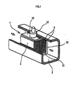
FIG. 1 is a partially cut-away perspective view of a duct to which a ceramic heater according to one embodiment of the present invention is incorporated; and -
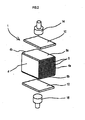
FIG. 2 is an exploded perspective view of the ceramic heater. - As shown in
FIGS. 1 and2 , a ceramic heater 1 is housed inside a duct 2. In the present embodiment, a fluid which is to be flowed through inside the duct 2 is air. However, the fluid is not limited to air, and may be a gas other than air or may be a liquid such as water, etc. - The ceramic heater 1 includes a ceramic resistor 4 having a generally honeycomb structure. More specifically, the ceramic resistor 4 of the present embodiment is divided by a plurality of longitudinal ribs and a plurality of lateral ribs in a grid-like manner, so that a plurality of rectangular through holes 6 are formed in the ceramic resistor 4.
- The ceramic resistor 4 constituted as above is formed as follows: main materials such as silicon carbide and metallic silicon are first mixed together, added with water, and then kneaded; the resulting mixture is extruded and molded into a honeycomb structure; the molded main materials in honeycomb structure are reacted and sintered in a furnace under a nitrogen (inert gas) atmosphere; and as a result, the ceramic resistor 4, which is a composite of silicon carbide and silicon nitride, is formed.
- The ceramic resistor 4 has electrical conductivity, and is porous as explained above. In the present embodiment, the ceramic resistor 4 has an appearance of a cuboid shaped hexahedron. The through holes 6 have openings at
end surfaces end surfaces - Among the four surfaces, two opposing surfaces are assigned as a plane for an electrode (hereinafter referred to as "electrode plane").
Metallic films metallic films metallic films metallic films - Plate-like
foam metal members metallic films foam metal members metallic films - The
foam metal members - As a result of this evaporation, a plurality of very fine and uniformly-sized air bubbles are generated inside the compact, thereby forming the
foam metal members foam metal members foam metal members foam metal members foam metal members foam metal members - In the present embodiment, the
foam metal members metallic films metallic films foam metal members - Since the
metallic films foam metal members metallic films - In the ceramic heater 1, even if there are concaves and convexes or swells in the electrode planes on which the
metallic films foam metal members metallic films foam metal members metallic films foam metal members - For example, the small convexes in the electrode planes are entered into the air pores formed in attachment surfaces of the
foam metal members foam metal members foam metal members metallic films - Moreover, even if there is a swell in the electrode planes, the
foam metal members foam metal members metallic films - A
metal electrode 14 is attached to a generally central region of a surface of the plate-likefoam metal member 10. Likewise, ametal electrode 16 is attached to a generally central region of a surface of the plate-likefoam metal member 12. In the present embodiment, theelectrodes foam metal members - An attachment area between the
electrode 14 and thefoam metal member 10 is smaller than an apparent area of thefoam metal member 10. Likewise, an attachment area between theelectrode 16 and thefoam metal member 12 is smaller than an apparent area of thefoam metal member 12. - The
electrodes foam metal members foam metal members foam metal members - The apparent area of the
foam metal member 10 is an entire area of one surface of thefoam metal member 10. The one surface of thefoam metal member 10 includes both of the metal portions and the air-pore portions, and faces to theelectrode 14. Likewise, the apparent area of thefoam metal member 12 is an entire area of one surface of thefoam metal member 12. The one surface of thefoam metal member 12 includes both of the metal portions and the air-pore portions, and faces to theelectrode 16. - The above attachment areas are smaller than the respective apparent areas of the
foam metal members foam metal members - An attachment operation of three types of components (i.e., the
metallic films foam metal members electrodes 14 and 16) can be facilitated by the following procedure: firstly, overlaying thefoam metal member 10 onto themetallic film 8a formed on the ceramic resistor 4; then, further overlaying theelectrode 14 onto the abovefoam metal member 10; and performing diffusion-bonding to themetallic film 8a, thefoam metal member 10, and theelectrode 14, at the same time. The attachment operation of themetallic film 8b, thefoam metal member 12, and theelectrode 16 can be facilitated by the same procedure as above. - Since the aforementioned three types of components have been diffusion-bonded, a contact surface between the
metallic film 8a and thefoam metal member 10, and a contact surface between thefoam metal member 10 and theelectrode 14, are closely attached and metallically bonded to each other. Similarly, a contact surface between themetallic film 8b and thefoam metal member 12, and a contact surface between thefoam metal member 12 and theelectrode 16, are closely attached and metallically bonded to each other. - As above, since the contact surfaces do not directly come into contact with an outer environment, increase in electric resistance over time may be suppressed.
- If the contact surfaces are not metallically bonded to each other, electric resistance increases depending on portions of the ceramic heater 1 due to oxide layer generated over time in the contact surfaces. If the electric resistance varies depending on the portions of the ceramic heater 1, temperature-rise performance of the ceramic heater 1 may be biased depending on portions of the ceramic heater 1.
- On the other hand, if the contact surfaces are closely attached and metallically bonded to each other, bias in temperature-rise performance may be suppressed.
- To use the ceramic heater 1, the ceramic heater 1 is to be covered by a
flexible mat 20 which is not electrically conductive. Specifically, the ceramic heater 1 is covered by themat 20 such that the end surfaces 4a and 4b of the ceramic resistor 4 are not covered and that the surfaces of thefoam metal members electrodes mat 20. - The ceramic heater 1 covered by the
mat 20 is housed inside the duct 2. Each of theelectrodes electrodes - When the
electrodes electrodes foam metal members metallic films metallic films metallic films - Moreover, in the case that the attachment areas between the
foam metal members respective electrodes foam metal members foam metal members - The
foam metal members foam metal members electrodes - As explained above, since the ceramic heater 1 can be made compact in size, the ceramic heater 1 can be used to warm up a small room such as a vehicle interior and a bathroom, etc. or to warm up a specific spot in an area.
- The present invention should not be limited to the above-explained embodiment. Rather, the present invention can be implemented in various manners without departing from the scope of the present invention.
Claims (11)
- A ceramic heater (1) comprising:a ceramic resistor (4);at least one metallic film (8a, 8b) that is formed on at least one surface of the ceramic resistor (4), the at least one surface being assigned as at least one electrode plane; characterised in, that there is further
at least one foam metal member (10, 12) that is formed in a plate-like shape, the at least one foam metal member covering and being attached to the at least one metallic film (8a, 8b); andat least one electrode (14, 16) being attached to the at least one foam metal member (10, 12) and having a contact area with the at least one foam metal member (10, 12) smaller than an apparent area of the at least one foam metal member (10, 12), the apparent area being an entire area of one surface of the at least one foam metal member (10, 12). - The ceramic heater (1) according to Claim 1,
wherein the at least one electrode (14, 16) is attached to a generally central region of a surface of the at least one foam metal member (10, 12) so as to stand from the at least one foam metal member (10, 12) in a generally vertical direction. - The ceramic heater (1) according to Claim 1 or 2,
wherein the ceramic resistor (4) is hexahedron shaped;
wherein the at least one metallic film (8a, 8b) is two metallic films (8a, 8b) formed on a pair of opposing surfaces of the ceramic resistor (4);
wherein the at least one foam metal member (10, 12) is two foam metal members (10, 12) attached respectively to the two metallic films (8a, 8b); and
wherein the at least one electrode (14, 16) is two electrodes (14, 16) attached respectively to the two foam metal members (10, 12). - The ceramic heater (1) according to any one of Claims 1 to 3,
wherein the at least one electrode (14, 16) is attached to the at least one foam metal member (10, 12) by diffusion-bonding. - The ceramic heater (1) according to any one of Claims 1 to 4,
wherein the at least one electrode (14, 16) is metallically bonded to the at least one foam metal member (10, 12). - The ceramic heater (1) according to any one of claims 1 to 5,
wherein the at least one metallic film (8a, 8b) is formed over an entire area of the at least one electrode plane. - The ceramic heater (1) according to any one of Claims 1 to 6,
wherein the at least one foam metal member (10, 12) covers and is attached over an entire area of the at least one metallic film (8a, 8b). - The ceramic heater (1) according to any one of Claims 1 to 7,
wherein the at least one foam metal member (10, 12) is attached to the at least one metallic film (8a, 8b) by diffusion-bonding. - The ceramic heater (1) according to any one of Claims 1 to 8,
wherein the at least one foam metal member (10, 12) is metallically bonded to the at least one metallic film (8a, 8b). - The ceramic heater (1) according to any one of Claims 1 to 9,
wherein the ceramic resistor (4) is formed in a honeycomb shape. - A method for manufacturing a ceramic heater (1), comprising the step of:forming at least one metallic film (8a, 8b) on at least one surface of a ceramic resistor (4); characterised in that, the method further comprising the steps of:placing and attaching at least one foam metal member (10, 12), which is formed in a plate-like shape, over the at least one metallic film (8a, 8b); andattaching at least one electrode (14, 16) to the at least one foam metal member (10, 12); the at least one electrode (14, 16) having a contact area with the at least one foam metal member (10, 12) smaller than an apparent area of the at least one foam metal member (10, 12), and the apparent area being an entire area of one surface of the at least one foam metal member (10, 12).
Applications Claiming Priority (1)
| Application Number | Priority Date | Filing Date | Title |
|---|---|---|---|
| JP2011133303A JP5937304B2 (en) | 2011-06-15 | 2011-06-15 | Ceramic heater |
Publications (2)
| Publication Number | Publication Date |
|---|---|
| EP2535904A1 EP2535904A1 (en) | 2012-12-19 |
| EP2535904B1 true EP2535904B1 (en) | 2014-09-03 |
Family
ID=46384116
Family Applications (1)
| Application Number | Title | Priority Date | Filing Date |
|---|---|---|---|
| EP12004535.6A Not-in-force EP2535904B1 (en) | 2011-06-15 | 2012-06-15 | Ceramic heater, and manufacturing method thereof |
Country Status (3)
| Country | Link |
|---|---|
| US (1) | US20120318784A1 (en) |
| EP (1) | EP2535904B1 (en) |
| JP (1) | JP5937304B2 (en) |
Families Citing this family (2)
| Publication number | Priority date | Publication date | Assignee | Title |
|---|---|---|---|---|
| CN106556138A (en) * | 2016-10-31 | 2017-04-05 | 江阴市国豪电热电器制造有限公司 | A kind of air duct type electric heater of homogeneous heating |
| JP2019036571A (en) * | 2017-08-10 | 2019-03-07 | Koa株式会社 | Manufacturing method of resistor |
Family Cites Families (12)
| Publication number | Priority date | Publication date | Assignee | Title |
|---|---|---|---|---|
| US2718577A (en) * | 1953-02-13 | 1955-09-20 | Wiegand Co Edwin L | Electric heating devices |
| US3163841A (en) * | 1962-01-02 | 1964-12-29 | Corning Glass Works | Electric resistance heater |
| US3956614A (en) * | 1975-04-21 | 1976-05-11 | Universal Oil Products Company | Electric current distribution means for a ceramic type of electrical resistance heater element |
| JPS58184287A (en) * | 1982-04-20 | 1983-10-27 | 日本特殊陶業株式会社 | Honeycomb type heater |
| US4922163A (en) * | 1988-12-08 | 1990-05-01 | Westinghouse Electric Corp. | Actively cooled brush box assembly |
| JPH09106883A (en) * | 1996-08-29 | 1997-04-22 | Sharp Corp | Ceramic heater manufacturing method |
| DE19854173C2 (en) * | 1998-11-24 | 2000-11-23 | Fritz Michael Streuber | Metal foam molded body |
| JP2001319760A (en) * | 2000-05-09 | 2001-11-16 | Narumi China Corp | Heater substrate |
| JP2002367810A (en) * | 2001-06-11 | 2002-12-20 | Nec Tokin Corp | Macromolecular ptc element and its manufacturing method |
| JP2005237140A (en) * | 2004-02-20 | 2005-09-02 | Toyota Motor Corp | Substrate and substrate wiring method |
| DE102008017157B4 (en) * | 2008-04-03 | 2022-10-06 | Vitesco Technologies GmbH | Contact element and printed circuit board arrangement |
| US8327911B2 (en) * | 2009-08-09 | 2012-12-11 | Rolls-Royce Corporation | Method for forming a cast article |
-
2011
- 2011-06-15 JP JP2011133303A patent/JP5937304B2/en not_active Expired - Fee Related
-
2012
- 2012-06-15 EP EP12004535.6A patent/EP2535904B1/en not_active Not-in-force
- 2012-06-15 US US13/524,004 patent/US20120318784A1/en not_active Abandoned
Also Published As
| Publication number | Publication date |
|---|---|
| JP2013004270A (en) | 2013-01-07 |
| EP2535904A1 (en) | 2012-12-19 |
| JP5937304B2 (en) | 2016-06-22 |
| US20120318784A1 (en) | 2012-12-20 |
Similar Documents
| Publication | Publication Date | Title |
|---|---|---|
| US8071913B2 (en) | Heating device | |
| RU2550799C2 (en) | High-temperature high performance thermoelectric module | |
| US20190359032A1 (en) | Radiant heater device | |
| JP6342769B2 (en) | Electrostatic chuck | |
| JP6625468B2 (en) | Honeycomb structure and manufacturing method thereof | |
| US20060032622A1 (en) | Thermal assembly and method for fabricating the same | |
| CN107226708B (en) | Bonded body and method for producing bonded body | |
| CN112292738B (en) | Ceramic multilayer component and method for producing a ceramic multilayer component | |
| JP6632885B2 (en) | Thermal switch element | |
| JP2017112353A (en) | Chip resistor | |
| JP2019522349A (en) | Thermoelectric leg and thermoelectric element including the same | |
| JP6547641B2 (en) | heatsink | |
| JP6554379B2 (en) | Zygote | |
| EP2535904A1 (en) | Ceramic heater, and manufacturing method thereof | |
| JP2016074587A (en) | Bonded body and method of manufacturing the bonded body | |
| CN105659399A (en) | Thermoelectric conversion device having thermoelectric conversion element connected thereto via wiring pattern, and method for manufacturing thermoelectric conversion device having thermoelectric conversion element connected thereto via wiring pattern | |
| JP7686884B1 (en) | Semiconductor manufacturing equipment parts | |
| KR102713025B1 (en) | Wafer loading platform | |
| JP6093130B2 (en) | heater | |
| US9242445B2 (en) | Method for producing bonded body | |
| JP7075335B2 (en) | Multilayer board and its manufacturing method | |
| JP2011175837A (en) | Ceramic heater | |
| JP5517816B2 (en) | Ceramic body with conductive layer, and joined body of ceramic and metal | |
| JP7017967B2 (en) | Heater and heater system | |
| WO2022075172A1 (en) | Porous body, heat-dissipating structure, and electronic apparatus |
Legal Events
| Date | Code | Title | Description |
|---|---|---|---|
| PUAI | Public reference made under article 153(3) epc to a published international application that has entered the european phase |
Free format text: ORIGINAL CODE: 0009012 |
|
| AK | Designated contracting states |
Kind code of ref document: A1 Designated state(s): AL AT BE BG CH CY CZ DE DK EE ES FI FR GB GR HR HU IE IS IT LI LT LU LV MC MK MT NL NO PL PT RO RS SE SI SK SM TR |
|
| AX | Request for extension of the european patent |
Extension state: BA ME |
|
| 17P | Request for examination filed |
Effective date: 20130618 |
|
| RBV | Designated contracting states (corrected) |
Designated state(s): AL AT BE BG CH CY CZ DE DK EE ES FI FR GB GR HR HU IE IS IT LI LT LU LV MC MK MT NL NO PL PT RO RS SE SI SK SM TR |
|
| GRAP | Despatch of communication of intention to grant a patent |
Free format text: ORIGINAL CODE: EPIDOSNIGR1 |
|
| INTG | Intention to grant announced |
Effective date: 20140207 |
|
| RIN1 | Information on inventor provided before grant (corrected) |
Inventor name: KOBAYASHI, ARATA Inventor name: HAMADA, KAZUICHI |
|
| GRAP | Despatch of communication of intention to grant a patent |
Free format text: ORIGINAL CODE: EPIDOSNIGR1 |
|
| GRAS | Grant fee paid |
Free format text: ORIGINAL CODE: EPIDOSNIGR3 |
|
| INTG | Intention to grant announced |
Effective date: 20140528 |
|
| RAP1 | Party data changed (applicant data changed or rights of an application transferred) |
Owner name: FUTABA INDUSTRIAL CO. LTD. |
|
| GRAA | (expected) grant |
Free format text: ORIGINAL CODE: 0009210 |
|
| AK | Designated contracting states |
Kind code of ref document: B1 Designated state(s): AL AT BE BG CH CY CZ DE DK EE ES FI FR GB GR HR HU IE IS IT LI LT LU LV MC MK MT NL NO PL PT RO RS SE SI SK SM TR |
|
| REG | Reference to a national code |
Ref country code: GB Ref legal event code: FG4D |
|
| REG | Reference to a national code |
Ref country code: AT Ref legal event code: REF Ref document number: 685965 Country of ref document: AT Kind code of ref document: T Effective date: 20140915 Ref country code: CH Ref legal event code: EP |
|
| REG | Reference to a national code |
Ref country code: IE Ref legal event code: FG4D |
|
| REG | Reference to a national code |
Ref country code: DE Ref legal event code: R096 Ref document number: 602012002916 Country of ref document: DE Effective date: 20141016 |
|
| REG | Reference to a national code |
Ref country code: SE Ref legal event code: TRGR |
|
| REG | Reference to a national code |
Ref country code: AT Ref legal event code: MK05 Ref document number: 685965 Country of ref document: AT Kind code of ref document: T Effective date: 20140903 |
|
| PG25 | Lapsed in a contracting state [announced via postgrant information from national office to epo] |
Ref country code: ES Free format text: LAPSE BECAUSE OF FAILURE TO SUBMIT A TRANSLATION OF THE DESCRIPTION OR TO PAY THE FEE WITHIN THE PRESCRIBED TIME-LIMIT Effective date: 20140903 Ref country code: GR Free format text: LAPSE BECAUSE OF FAILURE TO SUBMIT A TRANSLATION OF THE DESCRIPTION OR TO PAY THE FEE WITHIN THE PRESCRIBED TIME-LIMIT Effective date: 20141204 Ref country code: LT Free format text: LAPSE BECAUSE OF FAILURE TO SUBMIT A TRANSLATION OF THE DESCRIPTION OR TO PAY THE FEE WITHIN THE PRESCRIBED TIME-LIMIT Effective date: 20140903 Ref country code: NO Free format text: LAPSE BECAUSE OF FAILURE TO SUBMIT A TRANSLATION OF THE DESCRIPTION OR TO PAY THE FEE WITHIN THE PRESCRIBED TIME-LIMIT Effective date: 20141203 Ref country code: FI Free format text: LAPSE BECAUSE OF FAILURE TO SUBMIT A TRANSLATION OF THE DESCRIPTION OR TO PAY THE FEE WITHIN THE PRESCRIBED TIME-LIMIT Effective date: 20140903 |
|
| REG | Reference to a national code |
Ref country code: NL Ref legal event code: VDEP Effective date: 20140903 |
|
| REG | Reference to a national code |
Ref country code: LT Ref legal event code: MG4D |
|
| PG25 | Lapsed in a contracting state [announced via postgrant information from national office to epo] |
Ref country code: LV Free format text: LAPSE BECAUSE OF FAILURE TO SUBMIT A TRANSLATION OF THE DESCRIPTION OR TO PAY THE FEE WITHIN THE PRESCRIBED TIME-LIMIT Effective date: 20140903 Ref country code: RS Free format text: LAPSE BECAUSE OF FAILURE TO SUBMIT A TRANSLATION OF THE DESCRIPTION OR TO PAY THE FEE WITHIN THE PRESCRIBED TIME-LIMIT Effective date: 20140903 Ref country code: CY Free format text: LAPSE BECAUSE OF FAILURE TO SUBMIT A TRANSLATION OF THE DESCRIPTION OR TO PAY THE FEE WITHIN THE PRESCRIBED TIME-LIMIT Effective date: 20140903 Ref country code: HR Free format text: LAPSE BECAUSE OF FAILURE TO SUBMIT A TRANSLATION OF THE DESCRIPTION OR TO PAY THE FEE WITHIN THE PRESCRIBED TIME-LIMIT Effective date: 20140903 Ref country code: AT Free format text: LAPSE BECAUSE OF FAILURE TO SUBMIT A TRANSLATION OF THE DESCRIPTION OR TO PAY THE FEE WITHIN THE PRESCRIBED TIME-LIMIT Effective date: 20140903 |
|
| PG25 | Lapsed in a contracting state [announced via postgrant information from national office to epo] |
Ref country code: NL Free format text: LAPSE BECAUSE OF FAILURE TO SUBMIT A TRANSLATION OF THE DESCRIPTION OR TO PAY THE FEE WITHIN THE PRESCRIBED TIME-LIMIT Effective date: 20140903 |
|
| RAP2 | Party data changed (patent owner data changed or rights of a patent transferred) |
Owner name: FUTABA INDUSTRIAL CO. LTD. |
|
| PG25 | Lapsed in a contracting state [announced via postgrant information from national office to epo] |
Ref country code: RO Free format text: LAPSE BECAUSE OF FAILURE TO SUBMIT A TRANSLATION OF THE DESCRIPTION OR TO PAY THE FEE WITHIN THE PRESCRIBED TIME-LIMIT Effective date: 20140903 Ref country code: PT Free format text: LAPSE BECAUSE OF FAILURE TO SUBMIT A TRANSLATION OF THE DESCRIPTION OR TO PAY THE FEE WITHIN THE PRESCRIBED TIME-LIMIT Effective date: 20150105 Ref country code: SK Free format text: LAPSE BECAUSE OF FAILURE TO SUBMIT A TRANSLATION OF THE DESCRIPTION OR TO PAY THE FEE WITHIN THE PRESCRIBED TIME-LIMIT Effective date: 20140903 Ref country code: IS Free format text: LAPSE BECAUSE OF FAILURE TO SUBMIT A TRANSLATION OF THE DESCRIPTION OR TO PAY THE FEE WITHIN THE PRESCRIBED TIME-LIMIT Effective date: 20150103 Ref country code: EE Free format text: LAPSE BECAUSE OF FAILURE TO SUBMIT A TRANSLATION OF THE DESCRIPTION OR TO PAY THE FEE WITHIN THE PRESCRIBED TIME-LIMIT Effective date: 20140903 |
|
| PG25 | Lapsed in a contracting state [announced via postgrant information from national office to epo] |
Ref country code: PL Free format text: LAPSE BECAUSE OF FAILURE TO SUBMIT A TRANSLATION OF THE DESCRIPTION OR TO PAY THE FEE WITHIN THE PRESCRIBED TIME-LIMIT Effective date: 20140903 |
|
| REG | Reference to a national code |
Ref country code: DE Ref legal event code: R097 Ref document number: 602012002916 Country of ref document: DE |
|
| PLBE | No opposition filed within time limit |
Free format text: ORIGINAL CODE: 0009261 |
|
| STAA | Information on the status of an ep patent application or granted ep patent |
Free format text: STATUS: NO OPPOSITION FILED WITHIN TIME LIMIT |
|
| PG25 | Lapsed in a contracting state [announced via postgrant information from national office to epo] |
Ref country code: DK Free format text: LAPSE BECAUSE OF FAILURE TO SUBMIT A TRANSLATION OF THE DESCRIPTION OR TO PAY THE FEE WITHIN THE PRESCRIBED TIME-LIMIT Effective date: 20140903 |
|
| 26N | No opposition filed |
Effective date: 20150604 |
|
| PG25 | Lapsed in a contracting state [announced via postgrant information from national office to epo] |
Ref country code: IT Free format text: LAPSE BECAUSE OF FAILURE TO SUBMIT A TRANSLATION OF THE DESCRIPTION OR TO PAY THE FEE WITHIN THE PRESCRIBED TIME-LIMIT Effective date: 20140903 |
|
| PG25 | Lapsed in a contracting state [announced via postgrant information from national office to epo] |
Ref country code: SI Free format text: LAPSE BECAUSE OF FAILURE TO SUBMIT A TRANSLATION OF THE DESCRIPTION OR TO PAY THE FEE WITHIN THE PRESCRIBED TIME-LIMIT Effective date: 20140903 |
|
| PG25 | Lapsed in a contracting state [announced via postgrant information from national office to epo] |
Ref country code: MC Free format text: LAPSE BECAUSE OF FAILURE TO SUBMIT A TRANSLATION OF THE DESCRIPTION OR TO PAY THE FEE WITHIN THE PRESCRIBED TIME-LIMIT Effective date: 20140903 |
|
| REG | Reference to a national code |
Ref country code: CH Ref legal event code: PL |
|
| PG25 | Lapsed in a contracting state [announced via postgrant information from national office to epo] |
Ref country code: LU Free format text: LAPSE BECAUSE OF FAILURE TO SUBMIT A TRANSLATION OF THE DESCRIPTION OR TO PAY THE FEE WITHIN THE PRESCRIBED TIME-LIMIT Effective date: 20150615 |
|
| REG | Reference to a national code |
Ref country code: IE Ref legal event code: MM4A |
|
| PG25 | Lapsed in a contracting state [announced via postgrant information from national office to epo] |
Ref country code: CH Free format text: LAPSE BECAUSE OF NON-PAYMENT OF DUE FEES Effective date: 20150630 Ref country code: LI Free format text: LAPSE BECAUSE OF NON-PAYMENT OF DUE FEES Effective date: 20150630 Ref country code: IE Free format text: LAPSE BECAUSE OF NON-PAYMENT OF DUE FEES Effective date: 20150615 |
|
| REG | Reference to a national code |
Ref country code: FR Ref legal event code: PLFP Year of fee payment: 5 |
|
| PG25 | Lapsed in a contracting state [announced via postgrant information from national office to epo] |
Ref country code: BE Free format text: LAPSE BECAUSE OF FAILURE TO SUBMIT A TRANSLATION OF THE DESCRIPTION OR TO PAY THE FEE WITHIN THE PRESCRIBED TIME-LIMIT Effective date: 20140903 |
|
| PGFP | Annual fee paid to national office [announced via postgrant information from national office to epo] |
Ref country code: GB Payment date: 20160621 Year of fee payment: 5 Ref country code: CZ Payment date: 20160614 Year of fee payment: 5 |
|
| PGFP | Annual fee paid to national office [announced via postgrant information from national office to epo] |
Ref country code: FR Payment date: 20160627 Year of fee payment: 5 Ref country code: SE Payment date: 20160620 Year of fee payment: 5 |
|
| PG25 | Lapsed in a contracting state [announced via postgrant information from national office to epo] |
Ref country code: MT Free format text: LAPSE BECAUSE OF FAILURE TO SUBMIT A TRANSLATION OF THE DESCRIPTION OR TO PAY THE FEE WITHIN THE PRESCRIBED TIME-LIMIT Effective date: 20140903 |
|
| PG25 | Lapsed in a contracting state [announced via postgrant information from national office to epo] |
Ref country code: SM Free format text: LAPSE BECAUSE OF FAILURE TO SUBMIT A TRANSLATION OF THE DESCRIPTION OR TO PAY THE FEE WITHIN THE PRESCRIBED TIME-LIMIT Effective date: 20140903 Ref country code: HU Free format text: LAPSE BECAUSE OF FAILURE TO SUBMIT A TRANSLATION OF THE DESCRIPTION OR TO PAY THE FEE WITHIN THE PRESCRIBED TIME-LIMIT; INVALID AB INITIO Effective date: 20120615 Ref country code: BG Free format text: LAPSE BECAUSE OF FAILURE TO SUBMIT A TRANSLATION OF THE DESCRIPTION OR TO PAY THE FEE WITHIN THE PRESCRIBED TIME-LIMIT Effective date: 20140903 |
|
| PG25 | Lapsed in a contracting state [announced via postgrant information from national office to epo] |
Ref country code: TR Free format text: LAPSE BECAUSE OF FAILURE TO SUBMIT A TRANSLATION OF THE DESCRIPTION OR TO PAY THE FEE WITHIN THE PRESCRIBED TIME-LIMIT Effective date: 20140903 |
|
| REG | Reference to a national code |
Ref country code: SE Ref legal event code: EUG |
|
| PG25 | Lapsed in a contracting state [announced via postgrant information from national office to epo] |
Ref country code: CZ Free format text: LAPSE BECAUSE OF NON-PAYMENT OF DUE FEES Effective date: 20170615 |
|
| GBPC | Gb: european patent ceased through non-payment of renewal fee |
Effective date: 20170615 |
|
| PG25 | Lapsed in a contracting state [announced via postgrant information from national office to epo] |
Ref country code: SE Free format text: LAPSE BECAUSE OF NON-PAYMENT OF DUE FEES Effective date: 20170616 |
|
| REG | Reference to a national code |
Ref country code: FR Ref legal event code: ST Effective date: 20180228 |
|
| PG25 | Lapsed in a contracting state [announced via postgrant information from national office to epo] |
Ref country code: GB Free format text: LAPSE BECAUSE OF NON-PAYMENT OF DUE FEES Effective date: 20170615 |
|
| PG25 | Lapsed in a contracting state [announced via postgrant information from national office to epo] |
Ref country code: FR Free format text: LAPSE BECAUSE OF NON-PAYMENT OF DUE FEES Effective date: 20170630 |
|
| PG25 | Lapsed in a contracting state [announced via postgrant information from national office to epo] |
Ref country code: MK Free format text: LAPSE BECAUSE OF FAILURE TO SUBMIT A TRANSLATION OF THE DESCRIPTION OR TO PAY THE FEE WITHIN THE PRESCRIBED TIME-LIMIT Effective date: 20140903 |
|
| PGFP | Annual fee paid to national office [announced via postgrant information from national office to epo] |
Ref country code: DE Payment date: 20180625 Year of fee payment: 7 |
|
| PG25 | Lapsed in a contracting state [announced via postgrant information from national office to epo] |
Ref country code: AL Free format text: LAPSE BECAUSE OF FAILURE TO SUBMIT A TRANSLATION OF THE DESCRIPTION OR TO PAY THE FEE WITHIN THE PRESCRIBED TIME-LIMIT Effective date: 20140903 |
|
| REG | Reference to a national code |
Ref country code: DE Ref legal event code: R119 Ref document number: 602012002916 Country of ref document: DE |
|
| PG25 | Lapsed in a contracting state [announced via postgrant information from national office to epo] |
Ref country code: DE Free format text: LAPSE BECAUSE OF NON-PAYMENT OF DUE FEES Effective date: 20200101 |