EP2533608A1 - Multiple channel light source power supply with output protection - Google Patents
Multiple channel light source power supply with output protection Download PDFInfo
- Publication number
- EP2533608A1 EP2533608A1 EP12170919A EP12170919A EP2533608A1 EP 2533608 A1 EP2533608 A1 EP 2533608A1 EP 12170919 A EP12170919 A EP 12170919A EP 12170919 A EP12170919 A EP 12170919A EP 2533608 A1 EP2533608 A1 EP 2533608A1
- Authority
- EP
- European Patent Office
- Prior art keywords
- converter circuits
- circuit
- voltage converter
- output
- current
- Prior art date
- Legal status (The legal status is an assumption and is not a legal conclusion. Google has not performed a legal analysis and makes no representation as to the accuracy of the status listed.)
- Granted
Links
Images


Classifications
-
- H—ELECTRICITY
- H05—ELECTRIC TECHNIQUES NOT OTHERWISE PROVIDED FOR
- H05B—ELECTRIC HEATING; ELECTRIC LIGHT SOURCES NOT OTHERWISE PROVIDED FOR; CIRCUIT ARRANGEMENTS FOR ELECTRIC LIGHT SOURCES, IN GENERAL
- H05B47/00—Circuit arrangements for operating light sources in general, i.e. where the type of light source is not relevant
- H05B47/20—Responsive to malfunctions or to light source life; for protection
- H05B47/23—Responsive to malfunctions or to light source life; for protection of two or more light sources connected in series
-
- H—ELECTRICITY
- H05—ELECTRIC TECHNIQUES NOT OTHERWISE PROVIDED FOR
- H05B—ELECTRIC HEATING; ELECTRIC LIGHT SOURCES NOT OTHERWISE PROVIDED FOR; CIRCUIT ARRANGEMENTS FOR ELECTRIC LIGHT SOURCES, IN GENERAL
- H05B45/00—Circuit arrangements for operating light-emitting diodes [LED]
- H05B45/50—Circuit arrangements for operating light-emitting diodes [LED] responsive to malfunctions or undesirable behaviour of LEDs; responsive to LED life; Protective circuits
- H05B45/54—Circuit arrangements for operating light-emitting diodes [LED] responsive to malfunctions or undesirable behaviour of LEDs; responsive to LED life; Protective circuits in a series array of LEDs
-
- Y—GENERAL TAGGING OF NEW TECHNOLOGICAL DEVELOPMENTS; GENERAL TAGGING OF CROSS-SECTIONAL TECHNOLOGIES SPANNING OVER SEVERAL SECTIONS OF THE IPC; TECHNICAL SUBJECTS COVERED BY FORMER USPC CROSS-REFERENCE ART COLLECTIONS [XRACs] AND DIGESTS
- Y02—TECHNOLOGIES OR APPLICATIONS FOR MITIGATION OR ADAPTATION AGAINST CLIMATE CHANGE
- Y02B—CLIMATE CHANGE MITIGATION TECHNOLOGIES RELATED TO BUILDINGS, e.g. HOUSING, HOUSE APPLIANCES OR RELATED END-USER APPLICATIONS
- Y02B20/00—Energy efficient lighting technologies, e.g. halogen lamps or gas discharge lamps
- Y02B20/30—Semiconductor lamps, e.g. solid state lamps [SSL] light emitting diodes [LED] or organic LED [OLED]
Definitions
- the protection switch 112 may be any component or group of components having a conducting or "closed” state and a non-conducting or “open” state.
- the protection switch 112 may include a transistor.
- the output DC reg of the front end circuit 102 is coupled to the plurality of voltage converter circuits 106-1, 106-2, ... 106-N, and when the protection switch is in a non-conducting or "open” state, the output DC reg of the front end circuit 102 is decoupled from the plurality of voltage converter circuits 106-1, 106-2, ... 106-N.
- Each of the voltage converter circuits in the plurality of voltage converter circuits 106a-1 ... 106a-N shown in FIG. 2 may have the same buck converter configuration.
- the voltage converter 106a-N for example, includes a metal-oxide field effect transistor (MOSFET) QN which acts as a switch, a switch controller 204-N, a resistor RN, a diode DN, and an inductor LN.
- MOSFET metal-oxide field effect transistor
- 106a-N particularly the plurality of switches Q1... QN, are coupled to the low side of the output DC reg of the front end circuit 102 through the protection switch 112a and the current sense circuit 116a.
- the protection switch 112a when the protection switch 112a is in a conducting or "closed” (i.e., "on") state, the low side of the output DC reg of the front end circuit 102 is coupled to the plurality of voltage converter circuits 106a-1 ... 106a-N, but when the protection switch 112a is in a non-conducting or "open” (i.e., "off”) state, the low side of the output DC reg of the front end circuit 102 is decoupled from the plurality of voltage converter circuits 106a-1 ... 106a-N, thereby disabling the supply of power to the outputs/channels of the power supply circuit 100a.
- the controller circuit 114b When the current through the resistor Rsense (i.e., the current sense circuit 116b), and hence the voltage V Sense , provided to an input of the controller circuit 114b exceeds a predetermined level, there may be a short or fault in one or more of the plurality of voltage converter circuits 106a-1 ... 106a-N. In response to the voltage V Sense exceeding the predetermined level, therefore, the controller circuit 114b is configured to provide an output to a gate of the BJT 302 through the resistors Rd and Rc to place the BJT 302 in a conducting state.
- the switch controllers 204-1 ... 204-N place the plurality of switches Q2 ... QN in a non-conducting ("open") state, thereby disabling power delivery to the associated light sources 108a-1 ... 108a-N when the switches are functioning properly.
- FIG. 5 illustrates one embodiment of a current sense circuit 116c including a bypass switch 502 and a current sensor 504.
- the current sensor 504 may be configured as one or more resistors (e.g. Rsense shown in FIGs. 2 , 3 , and 6 ), coupled between the low side output of the front end circuit 102 and the plurality of voltage converter circuits 106-1, 106-2, ... 106-N, e.g. directly as shown in FIG. 3 or through the protection switch 112a as shown in FIG. 2 .
- the voltage V Sense across the current sensor 504 may be provided as an input to the controller circuit 114.
- the controller circuit 114 may provide an output to the switch controllers of the voltage converter circuits 106a-1 ... 106a-N to disable delivery of power delivery of power to the light sources 108a-1 ... 108a-N and may provide a bypass control signal to the bypass switch 502 to place the bypass switch in a non-conducting (or "open") state.
- the control circuit 114 may provide an output to the switch controllers of the voltage converter circuits 106a-1 ... 106a-N to enable delivery of power delivery of power to the light sources 108a-1 ... 108a-N and may also provide a bypass control signal to the bypass switch 502 to place the bypass switch 502 in a conducting (or "closed) state.
- the current I Sense is shunted around the current sensor 504 through the bypass switch 502. Any resistive loss associated with the current sense circuit 116c is thus reduced or eliminated resulting in improved efficiency compared to a configuration that does not include a bypass switch 502.
- a front end circuit is decoupled from the plurality of voltage converter circuits, step 705, when the current sense output exceeds the predetermined level.
- a state of a protection switch coupled between the front end circuit and the plurality of voltage converter circuits is changed, step 708.
- the bypass switch is placed in a conducting state to shunt current around the current sensor, and each voltage converter circuit in the plurality of voltage converter circuits is enabled, so that the plurality of voltage converter circuits are functioning to supply power to one or more light sources connected to the one or more output channels, step 706, when the current sense output does not exceed the predetermined level.
Landscapes
- Dc-Dc Converters (AREA)
- Circuit Arrangement For Electric Light Sources In General (AREA)
Abstract
Description
- The present invention relates to lighting, and more specifically, to power supplies for lighting.
- Certain power supplies used in the United States are subject to the safety regulations established by the Underwriters Laboratory, particularly the UL1310 Class 2 standard. The UL1310 standard limits the voltage, current, and power of each output of power supplies classified as Class 2 supplies. These limits must be met even under single component fault conditions. The power limit on a UL1310 Class 2 power supply, for example, is currently 100 Watts per output channel. Each channel/output of a power supply may be configured to drive a separate light source, e.g. a solid state light source (i.e., light-emitting diode (LED), organic light emitting diode (OLED), etc.), a gas-discharge lamp, or an incandescent lamp, among others.
- Such power supplies often utilize two voltage conversion stages, i.e. a front end stage and an output stage. The front end stage may receive an input voltage, e.g. a 120VAC voltage, and convert the input voltage to a regulated DC output voltage. The output stage may receive the DC output of the front end stage and provide a regulated DC output using a DC/ DC converter for each channel of the power supply. Each of the stages is thus capable of limiting the output voltage, current, and power.
- With a single channel power supply, the power limit of both the front end stage and the output stage may be set to less than 100 Watts, so that the stages serve as backups to each other. In a multiple channel/output power supply, each of the output channels, when combined, may be capable of delivering more than 100 Watts. Therefore, the output power limit of the front end stage in a multiple channel power supply may need to be set at higher than 100 Watts, and cannot serve to backup a potential single component fault in a single channel of the output stage.
- Perhaps the highest impact fault that may occur in a multiple channel/output power supply is when the regulation of one or more of the outputs is shorted (e.g., a MOSFET or inductor short of an output buck regulator), which may result in the faulty output delivering the maximum front end power on that single faulty channel. This is not likely an issue on a single channel/output power supply if the power limit of the front end is less than the 100 Watts maximum limit for the output per UL1310. However, this can be a significant issue when the faulty channel is in a multiple channel/output power supply, because the power limit for the front end is likely higher than 100 Watts.
- In some known configurations, the potential for a single faulty output channel delivering more than 100 Watts is addressed by providing additional protection circuitry on each output channel. The protection circuitry may monitor the voltage and current for each output channel, and may turn off the channel and/or the entire power supply if one of the values representing the voltage, current, or power is too high. The additional protection circuitry, however, requires more components and more space, adding both additional monetary and efficiency costs. Alternatively, of course, a power supply could simply offer no more than 100 Watts combined across all of its channels.
- Embodiments of the present invention provide a power supply with a protection circuit between a front end stage and an output stage, where the output stage includes a plurality of voltage converter circuits. Each of the voltage converter circuits provides a separate associated output to each output channel of the power supply. A current sense circuit is coupled to the voltage converter circuits and provides a current sense output to a controller circuit. When the current through one or more of the voltage converter circuits exceeds a pre-determined value as represented by the current sense output, the controller circuit provides an output to a protection switch for decoupling the output of the front end stage from the voltage converter circuits. According, if there is a short circuit or other fault in any of the voltage converter circuits of the output stage, all of the voltage converter circuits of the output stage are effectively turned "off" to avoid excessive power (e.g., power greater than 100 Watts) on any of the output power supply channels.
- In some embodiments, it may be desirable to reduce or eliminate inefficiency caused by resistive losses associated with the current sense circuit. In such embodiments, the current sense circuit may include a current sensor for providing the current sense output and a bypass switch coupled in parallel with the current sensor. To determine whether there are shorts in the one or more of the voltage converter circuits, the bypass switch may be placed in a non-conducting state so that current representative of current through the voltage converter circuit flows through the current sensor to establish the current sense output. If the current sense output exceeds the pre-determined threshold, the controller circuit provides an output to a protection switch for decoupling the output of the front end stage from the voltage converter circuits. If the current sense output does not exceed the pre-determined threshold, the controller circuit provides an output to the protection switch for coupling the output of the front end stage to the voltage converter circuits and places the bypass switch in a conducting state to shunt current around the current sensor. Shunting current around the current sensor when the power supply circuit is functioning normally to supply current to the voltage converter circuits reduces or eliminates inefficiency caused by resistive losses associated with the current sensor
- Embodiments of such a power supply circuit thus provide output protection for a multiple channel power supply without requiring additional circuitry on each channel of the power supply. This provides size, cost, reliability, and efficiency advantages. In addition, embodiments may include a current sense circuit that provides a current sense output that is a voltage output, thus providing very little additional energy losses as a result of the current sense circuit. Also, when the voltage converter circuits are decoupled from the front end stage by the protection switch, the front end stage may enter a standby mode, keeping the power consumption of the power supply low.
- In an embodiment, there is provided a light source power supply circuit having multiple output channels. The light source power supply circuit includes: a front end circuit configured to receive an input voltage and provide a regulated front end direct current (DC) voltage; a plurality of voltage converter circuits, each of the voltage converter circuits in the plurality of voltage converter circuits being configured to receive the regulated front end DC voltage and provide a separate associated DC output for an associated one of the multiple output channels; a protection switch coupled between the plurality of voltage converter circuits and the front end circuit, the protection switch having a conducting state to couple the front end DC voltage to the plurality of voltage converter circuits and a non-conducting state to decouple the front end DC voltage from the plurality of voltage converter circuits; a current sense circuit coupled to the plurality of voltage converter circuits, the current sense circuit including a current sensor and a bypass switch coupled in parallel with the current sensor, the bypass switch having a conducting state to shunt current around the current sensor and a non-conducting state to allow current to flow through the current sensor, whereby when the bypass switch is in the non-conducting state a voltage across the current sensor establishes a current sense output representative of current through at least one of the voltage converter circuits in the plurality of voltage converter circuits; and a controller circuit configured to place the protection switch in the non-conducting state in response to the current sense output.
- In a related embodiment, the plurality of voltage converter circuits may include a plurality of switches, and the controller circuit may be configured to provide an output to place a switch in the plurality of switches in a non-conducting state so that power is not delivered by the switch in the plurality of switches to a light source connected to an output channel of the light source power supply circuit associated with that switch.
- In another related embodiment, the protection switch may be coupled between a low side output of the front end circuit and the plurality of voltage converter circuits. In a further related embodiment, the plurality of voltage converter circuits may be a plurality of switching converter circuits, and the current sensor may include at least one resistor, the at least one resistor being coupled to each of the switching converter circuits in the plurality of switching converter circuits to sense current through the plurality of switching converter circuits, and the current sense output may include a voltage across the at least one resistor. In a further related embodiment, the protection switch may include a transistor having a gate coupled to the controller, a source coupled to the at least one resistor, and a drain coupled to each of the switching converter circuits in the plurality of switching converter circuits. In a further related embodiment, the drain may be coupled to a switch portion of each switching converter circuit in the plurality of switching converter circuits through a resistor.
- In yet another related embodiment, the protection switch may be coupled between a high side output of the front end circuit and the plurality of voltage converter circuits. In a further related embodiment, the current sensor may include at least one resistor coupled between a low side output of the front end circuit and ground, and the current sense output may include a voltage across the at least one resistor.
- In still another related embodiment, each of the voltage converter circuits in the plurality of voltage converter circuits may be configured as a buck converter. In another related embodiment, the bypass switch may include a transistor.
- In another embodiment, there is provided a multiple output channel light source power supply circuit. The multiple output channel light source power supply circuit includes: a front end circuit configured to receive an input voltage and provide a regulated front end direct current (DC) voltage; a plurality of voltage converter circuits, each of the voltage converter circuits being configured as a buck converter and configured to receive the regulated front end DC voltage and provide a separate associated DC output for an associated one of the multiple output channels; a protection switch coupled between the plurality of voltage converter circuits and a low side output of the front end circuit, the protection switch having a conducting state to couple the front end DC voltage to the plurality of voltage converter circuits and a non-conducting state to decouple the front end DC voltage from the plurality of voltage converter circuits; a current sense circuit coupled to the plurality of voltage converter circuits, the current sense circuit including a current sensor and a bypass switch coupled in parallel with the current sensor, the bypass switch having a conducting state to shunt current around the current sensor and a non-conducting state to allow current to flow through the current sensor, whereby when the bypass switch is in the non-conducting state a voltage across the current sensor establishes a current sense output representative of current through at least one of the voltage converter circuits; and a controller circuit configured to provide an output to place the protection switch in a non-conducting state so that power is not delivered to light sources connected to the multiple output channels, wherein the controller circuit provides the output in response to the current sense output.
- In a related embodiment, the protection switch may include a transistor having a gate coupled to the controller, a source coupled to at least one resistor, and a drain coupled to each of the voltage converter circuits in the plurality of voltage converter circuits. In a further related embodiment, the drain may be coupled to each of the voltage converter circuits in the plurality of voltage converter circuits through a resistor.
- In another related embodiment, the plurality of voltage converter circuits is a plurality of switching converter circuits, and the current sensor includes at least one resistor coupled to each of the switching converter circuits in the plurality of switching converter circuits. In another related embodiment, the bypass switch comprises a transistor.
- In another embodiment, there is provided a method of protecting against supplying excessive power at one or more output channels of a multiple output channel power supply. The method includes: placing a bypass switch in a non-conducting state, the bypass switch being coupled in parallel with a current sensor; disabling each voltage converter circuit in a plurality of voltage converter circuits, so that the plurality of voltage converter circuits are not functioning to supply power to one or more light sources connected to the one or more output channels; detecting a current through the current sensor to establish a current sense output representative of current through the plurality of voltage converter circuits after disabling; determining whether the current sense output exceeds a predetermined level; if the current sense output exceeds the predetermined level, decoupling a front end circuit from the plurality of voltage converter circuits; and if the current sense output does not exceed the predetermined level, then placing the bypass switch in a conducting state to shunt current around the current sensor, and enabling each voltage converter circuit in the plurality of voltage converter circuits, so that the plurality of voltage converter circuits are functioning to supply power to one or more light sources connected to the one or more output channels.
- In a related embodiment, disabling may include placing a switch portion of each of the voltage converter circuits in the plurality of voltage converter circuits in a non-conducting state. In another related embodiment, decoupling may include changing a state of a protection switch coupled between the front end circuit and the plurality of voltage converter circuits.
- The foregoing and other objects, features and advantages disclosed herein will be apparent from the following description of particular embodiments disclosed herein, as illustrated in the accompanying drawings in which like reference characters refer to the same parts throughout the different views. The drawings are not necessarily to scale, emphasis instead being placed upon illustrating the principles disclosed herein.
-
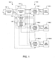
FIG. 1 shows a block diagram of a power supply according to embodiments disclosed herein. -
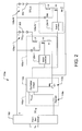
FIG. 2 is a circuit diagram of a power supply according to embodiments disclosed herein. -
FIG. 3 is another circuit diagram of a power supply according to embodiments disclosed herein. -
FIG. 4 is a block flow diagram of a method according to embodiments disclosed herein. -
FIG. 5 shows a block diagram of a current sense circuit according to embodiments disclosed herein. -
FIG. 6 is a circuit diagram of a power supply according to embodiments disclosed herein. -
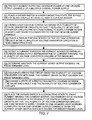
FIG. 7 is a block flow diagram of a method according to embodiments disclosed herein. -
FIG. 1 shows a simplified block diagram of apower supply circuit 100. Thepower supply circuit 100 includes a knownfront end circuit 102 and anoutput stage 104. Theoutput stage 104 includes a plurality of voltage converter circuits 106-1, 106-2, ... 106-N for driving separate associated light sources 108-1, 108-2, ... 108-N, and aprotection circuit 110. Theprotection circuit 110 includes aprotection switch 112, acontroller circuit 114, and acurrent sense circuit 116. Thefront end circuit 102 may include known circuit configurations for receiving an input voltage Vin, either directly or through a known dimmer circuit (not shown), and providing a regulated direct current (DC) output DCreg to the plurality of voltage converter circuits 106-1, 106-2, ... 106-N through theprotection circuit 110. In some embodiments, for example, the input voltage Vin may be an alternating current (AC) input provided directly from a 120VAC/60Hz line source. It is to be understood, however, that a system according to embodiments described herein may operate from a DC source or other AC sources, such as but not limited to a source providing 220-240 VAC at 50-60 Hz. - For example, the
front end circuit 102 may incorporate a known rectifier circuit for receiving the input voltage Vin, a known switching converter circuit, and a controller for controlling a switch within the switching converter. A variety of rectifier circuit configurations are well-known in the art. In some embodiments, for example, the rectifier circuit may include a known diode bridge rectifier or H-bridge rectifier. The switching converter circuit may receive the rectified AC output from the rectifier and provide the stable, regulated DC output DCreg to the plurality of voltage converter circuits 106-1, 106-2, ... 106-N through theprotection circuit 110. A variety of switching converter configurations, including, for example, buck converters, boost converters, buck-boost converters, etc., are well-known in the art. These devices generally include a switch, e.g. a transistor, which is selectively operated to allow energy to be stored in an energy storage device, e.g. an inductor, and then transferred to a load, such as a light source, e.g. using one or more filter capacitors. Another known type of switching converter includes a known transformer-based switching converter, such as a "flyback" converter. In a transformer-based switching converter, the primary side of the transformer may be coupled to the rectified AC output of the rectifier. The regulated DC output voltage is provided at the secondary side of the transformer, which is electrically isolated from the primary side of the transformer. - A variety of controllers for controlling the switch of a switching converter are well-known. In embodiments wherein the switching converter configuration is a buck converter, for example, the controller may be a model number TPS40050 controller presently available from Texas Instruments Corporation of Dallas, Texas, USA. The switching converter circuit may also include a known power factor correction (PFC) circuit.
- The plurality of voltage converter circuits 106-1, 106-2, ... 106-N may each include a known switching converter circuit (resulting in a plurality of switching converter circuits). The plurality of switching converter circuits may each include a switch (resulting in a plurality of switches), as described above. The plurality of switching converter circuits may include a known controller for controlling the plurality of switches. The plurality of voltage converter circuits 106-1, 106-2, ... 106-N may each receive the regulated DC output DCreg of the
front end circuit 102 and provide an associated DC output DCout1, DCout2, ... DCoutN to an associated one of the light sources 108-1, 108-2, ... 108-N. Each associated DC output DCout1, DCout2, ... DCoutN of a voltage converter circuit in the plurality of voltage converter circuits 106-1, 106-2, ... 106-N may be referred to herein as a "channel" or "output" of thepower supply circuit 100. The associated light sources 108-1, 108-2, ... 108-N may include any combination of any type of known light sources, such as but not limited to incandescent lamps, gas-discharge lamps, or solid state light sources. If an associated light source 108-1, 108-2, .. . 108-N is a solid state light source, it may include groups of solid state light sources (e.g., LED(s)) interconnected in series and/or parallel configurations. - Current through each of the voltage converter circuits in the plurality of voltage converter circuits 106-1, 106-2, ... 106-N may be fed back to the
current sense circuit 116, which may provide a current sense output to thecontroller circuit 114. In some embodiments, thecurrent sense circuit 116 may be configured as one or more resistors (shown inFIGs. 2 and3 ), and the current sense output may be a voltage across the resistor(s) that is representative of the current through one or more of the voltage converter circuits in the plurality of voltage converter circuits 106-1, 106-2, ... 106-N. When thecurrent sense circuit 116 provides a current sense output that exceeds a predefined threshold, thecontroller circuit 114 provides an output to theprotection switch 112 to change the conductive state of theprotection switch 112 from a state where the output DCreg of thefront end circuit 102 is coupled to the plurality of voltage converter circuits 106-1, 106-2, ... 106-N (i.e., a conducting state) to a state where the output DCreg of thefront end circuit 102 is decoupled from the plurality of voltage converter circuits 106-1, 106-2, ... 106-N (i.e., a non-conducting state). - The
protection switch 112 may be any component or group of components having a conducting or "closed" state and a non-conducting or "open" state. In some embodiments, for example, theprotection switch 112 may include a transistor. When theprotection switch 112 is in a conducting or "closed" state, the output DCreg of thefront end circuit 102 is coupled to the plurality of voltage converter circuits 106-1, 106-2, ... 106-N, and when the protection switch is in a non-conducting or "open" state, the output DCreg of thefront end circuit 102 is decoupled from the plurality of voltage converter circuits 106-1, 106-2, ... 106-N. Thecontroller circuit 114 may be any type of circuit configured to provide an output for changing the state of theprotection switch 112 in response to the current sense output of thecurrent sense circuit 116. For example, thecontroller circuit 114 may be a microcontroller configured to change the conduction state of theprotection switch 112 when the current sense output exceeds a predetermined threshold. - In embodiments wherein the plurality of voltage converter circuits 106-1, 106-2, . .. 106-N are configured as a plurality of switching converters including a plurality of switches, the
controller circuit 112 may also be configured to provide an output to each of the voltage converter circuits in the plurality of voltage converter circuits 106-1, 106-2, ... 106-N for placing the plurality of switches within the plurality of voltage converter circuits 106-1, 106-2, ... 106-N in a non-conducting or "open" state whereby, assuming there is no fault in the plurality of voltage converter switches 106-1, 106-2, ... 106-N, no power is provided to the associated light sources 108-1, 108-2, ... 108-N at the output of the plurality of voltage converter circuits 106-1, 106-2, ... 106-N. For example, thecontroller circuit 114 may be configured to disable the gate drive of a transistor switch of a switching converter in the plurality of switching converters, to thereby turn the switching converter off, so that no power is supplied to the associated light source by the transistor switch. - With this configuration, when the
controller circuit 114 turns the voltage converter circuits 106-1, 106-2, ... 106-N "off" (i.e., in a non-conducting / "open" state), there should be little or no current through the plurality of switches in the plurality of switching converters, and the current sense output of thecurrent sense circuit 116 should be below the predetermined threshold for causing a change in the conduction state of theprotection switch 112. However, in the event of, for example, a short occurring in a switch in the plurality of voltage converter circuits 106-1, 106-2, ... 106-N, e.g. across a transistor switch thereof, thecurrent sense circuit 116 will provide a current sense output to thecontroller circuit 114 that is above the pre-determined threshold. In response, thecontroller circuit 114 will change the conduction state of theprotection switch 112 to decouple the regulated DC output DCreg of thefront end circuit 102 from the plurality of voltage converter circuits 106-1, 106-2, ... 106-N. Accordingly, in thepower supply circuit 100, theprotection circuit 110 acts to protect against a fault in the plurality of voltage converter circuits 106-1, 106-2, ... 106-N that would potentially result in excessive power being supplied to one or more of the associated light sources 108-1, 108-2, ... 108-N. In some embodiments, for example, the component values of thecurrent sense circuit 116 and the predetermined threshold set in thecontroller circuit 114 may be established to decouple thefront end circuit 102 from the plurality of voltage converter circuits 106-1, 106-2, ... 106-N before a fault in one of the plurality of voltage converter circuits 106-1, 106-2, ... 106-N causes the power provided to an associated channel of thepower supply circuit 100 to exceed 100W, thereby providing compliance with the UL1310 class 2 standard. - A power supply (also referred to throughout as a "power supply circuit") according to embodiments described herein may be provided in a variety of configurations.
FIG. 2 illustrates apower supply circuit 100a, including afront end circuit 102, aprotection circuit 110a, and an output stage including a plurality ofvoltage converter circuits 106a-1 ... 106a-N, each of which is configured to provide an associated output/channel for driving an associatedlight source 108a-1 ... 108a-N. InFIG. 2 , the associatedlight sources 108a-1 ... 108a-N are configured as a plurality of series connectedlight emitting diodes 202. It is to be understood, however, that separate outputs/channels for driving any type of light source and/or different types of light sources on each channel may be used without departing from the scope of the invention. In embodiments where solid state light sources are among the associatedlight sources 108a-1 ... 108a-N, each of the solid state light sources may include any number of solid state light sources coupled in series, parallel, parallel combinations of series solid state light sources, or a single solid state light source. The operating characteristics and number of solid state light sources coupled to one of the outputs/channels of a power supply circuit according to embodiments described throughout may be different from the operating characteristics and number of solid state light sources coupled to another one of the outputs/channels. - In
FIG. 2 , the plurality ofvoltage converter circuits 106a-1 ... 106a-N are provided in a known buck converter configuration. Thevoltage converter circuit 106a-1, for example, includes a metal-oxide field effect transistor (MOSFET) Q2 that acts as a switch, a switch controller 204-1, a resistor R1, a diode D1, and an inductor L1. The source of the MOSFET Q2 is coupled to the low side of the output DCreg from thefront end circuit 102 through the resistor R1 and theprotection circuit 110a, and the drain of the MOSFET Q2 is coupled to the high side of the output DCreg from thefront end circuit 102 through the inductor L1 and the associatedlight source 108a-1. The diode D1 is coupled from the drain of the MOSFET Q2 to the high side of the output DCreg from thefront end circuit 102, and is reverse biased relative to the high side of the output DCreg from thefront end circuit 102. The switch controller 204-1 is coupled to the gate of the MOSFET Q2 for providing a pulse-width modulated (PWM) gate drive signal to open and close the MOSFET Q2 in a known manner. In some embodiments, for example, the switch controller 204-1 may be a model number TPS40050 controller presently available from Texas Instruments Corporation of Dallas, Texas, USA. - Each of the voltage converter circuits in the plurality of
voltage converter circuits 106a-1 ... 106a-N shown inFIG. 2 may have the same buck converter configuration. Thevoltage converter 106a-N, for example, includes a metal-oxide field effect transistor (MOSFET) QN which acts as a switch, a switch controller 204-N, a resistor RN, a diode DN, and an inductor LN. The source of the MOSFET QN is coupled to the low side of the output DCreg from thefront end circuit 102 through the resistor RN and theprotection circuit 110a, and the drain of the MOSFET QN is coupled to the high side of the output DCreg from thefront end circuit 102 through the inductor LN and the associatedlight source 108a-N. The diode DN is coupled from the drain of the MOSFET QN to the high side of the output DCreg from thefront end circuit 102, and is reverse biased relative to the high side of the output DCreg from thefront end circuit 102. The switch controller 204-N is coupled to the gate of the MOSFET QN for providing a PWM gate drive signal to open and close the MOSFET QN in a known manner. - The
protection circuit 110a includes aprotection switch 112a, acurrent sense circuit 116a, and acontroller circuit 114a. InFIG. 2 , theprotection switch 112a is configured as a MOSFET Q1, where the source of the MOSFET Q1 is coupled to the low side of the output DCreg of thefront end circuit 102 through thecurrent sense circuit 116a, which is configured as a resistor Rsense. The drain of the MOSFET Q1 is coupled to the source of each of the switches in the plurality of switches Q2 ... QN in the plurality ofvoltage converter circuits 106a-1 ... 106a-N through the resistors R1... RN, respectively. With this configuration, the plurality ofvoltage converter circuits 106a-1. .. 106a-N, particularly the plurality of switches Q1... QN, are coupled to the low side of the output DCreg of thefront end circuit 102 through theprotection switch 112a and thecurrent sense circuit 116a. Thus, when theprotection switch 112a is in a conducting or "closed" (i.e., "on") state, the low side of the output DCreg of thefront end circuit 102 is coupled to the plurality ofvoltage converter circuits 106a-1 ... 106a-N, but when theprotection switch 112a is in a non-conducting or "open" (i.e., "off") state, the low side of the output DCreg of thefront end circuit 102 is decoupled from the plurality ofvoltage converter circuits 106a-1 ... 106a-N, thereby disabling the supply of power to the outputs/channels of thepower supply circuit 100a. - The gate of the MOSFET Q1 is coupled to the
controller circuit 114a, and voltage VSense across the resistor Rsense is provided as an input to thecontroller circuit 114a. When the current through the resistor Rsense, and hence the voltage VSense, provided as an input to thecontroller circuit 114a exceeds a predetermined level, there may be a short or fault in one or more of the plurality ofvoltage converter circuits 106a-1 ... 106a-N. For example, there may be a short across the switch Q2 or the switch QN, leading to a potential for excess power delivered at the associated output/channel of thepower supply circuit 100a. In response to the voltage VSense exceeding the predetermined level, therefore, thecontroller circuit 114a is configured to provide an output to the gate of the MOSFET Q1 to place the MOSEFT Q1 in a non-conducting or "open" state, thereby decoupling the output DCreg from thefront end circuit 102 from the plurality ofvoltage converter circuits 106a-1... 106a-N and disabling supply of power to all the outputs/channels of thepower supply circuit 100a. - In
FIG. 2 , thecontroller circuit 114a is configured to provide an output to each of the switch controllers 204-1 ... 204-N in the plurality ofvoltage converter circuits 106a-1 ... 106a-N to enable and disable the PWM gate drive output of the switch controllers 204-1... 204-N to the plurality of switches Q2 ... QN. When the switch controllers 204-1... 204-N are enabled by the output of thecontroller circuit 114a, the PWM gate drive signals of the switch controllers 204-1 ... 204-N drive the gates of the plurality of switches Q2 ... QN to place the plurality of switches Q2 ... QN in alternately conducting ("closed") and non-conducting ("open") states to deliver power to the associatedlight sources 108a-1 ... 108a-N coupled thereto. When the switch controllers 204-1 ... 204-N are disabled by the output of thecontroller circuit 114a, the switch controllers 204-1... 204-N place the plurality of switches Q2... QN in a non-conducting ("open") state thereby disabling power delivery to the associatedlight sources 108a-1 ... 108a-N when the switches are functioning properly. - Faults or shorts in the plurality of
voltage converter circuits 106a-1 ... 106a-N that would potentially cause excessive power delivery to the outputs/channels of thepower supply circuit 100a may be detected by providing an output from thecontroller circuit 114a to the switch controllers 204-1... 204-N to place the plurality of switches Q2 ... QN in an non-conducting ("open") state and disable power delivery to the light sources. When the plurality of switches Q2 ... QN are placed in a non-conducting state, and Q1 is in a conducting ("closed") state, there should be very little current through the resistor Rsense if there is no fault in the plurality of switches Q2 ... QN. In such situations, the voltage VSense would not exceed the predetermined value set in thecontroller circuit 114a, and thecontroller circuit 114a would continue to provide an output to the gate of the MOSFET Q1 to keep the MOSFET Q1 in a conducting ("closed") state for coupling the output DCreg of thefront end circuit 102 to the plurality ofvoltage converter circuits 106a-1 ... 106a-N. Thecontroller circuit 114a may then provide an output to the switch controllers 204-1... 204-N to enable the gate drive output to the plurality of switches Q2... QN to resume normal operation and delivery of power to the associatedlight sources 108a-1 ... 108a-N. - However, in the event of a fault in one or more of the plurality of
voltage converter circuits 106a-1 ... 106a-N, such as a short across one or more of the switches in the plurality of switches Q2 ... QN, when the plurality of switches Q2 ... QN are placed in a non-conducting ("open') state, current may pass through the short, through the MOSFET Q1 and through the resistor Rsense. This may cause a voltage VSense that exceeds the predetermined value set in thecontroller circuit 114a. In response, thecontroller circuit 114a may provide an output to the gate of the MOSFET Q1 to place the MOSFET Q1 in a non-conducting state to decouple the output DCreg of thefront end circuit 102 from the plurality ofvoltage converter circuits 106a-1 ... 106a-N to thereby cease delivery of power to the output channels. - Another configuration of a
power supply circuit 100b is illustrated inFIG. 3 . Thepower supply circuit 100b includes afront end circuit 102, aprotection circuit 110b, and an output stage including a plurality ofvoltage converter circuits 106a-1 ... 106a-N, each of which is configured to provide an associated output/channel for driving an associatedlight source 108a-1 ... 108a-N. Thefront end circuit 102, the plurality ofvoltage converter circuits 106a-1 ... 106a-N, and the associatedlight sources 108a-1 ... 108a-N shown inFIG. 3 are the same as those shown and described in connection with thepower supply circuit 100a shown inFIG. 2 . For simplicity, the description of thefront end circuit 102, the plurality ofvoltage converter circuits 106a-1 ... 106a-N, and the associatedlight sources 108a-1 ... 108a-N will not be repeated in connection with thepower supply circuit 100b ofFIG. 3 . - The
protection circuit 110b ofFIG. 3 includes aprotection switch 112b, acurrent sense circuit 116b, and acontroller circuit 114b. Thecurrent sense circuit 116b is configured as a resistor Rsense through which the low side of the output DCreg of thefront end circuit 102 is coupled to ground. The sources of the plurality of switches Q2 .. . QN are coupled to ground through the resistors R1 ... RN, respectively. - The
protection switch 112b is configured as a MOSFET Q1 and a drain of the MOSFET Q1 is coupled to the high side of the output DCreg of thefront end circuit 102 through a resistor Ra. A source of the MOSFET Q1 is coupled to the drain of each of the switches in the plurality of switches Q2 ... QN in the plurality ofvoltage converter circuits 106a-1 ... 106a-N through the associatedlight sources 108a-1 ... 108a-N and the inductors L1 ... LN, respectively, and also through the reverse biased diodes D1... DN. With this configuration, the plurality ofvoltage converter circuits 106a-1 ... 106aN, particularly the plurality of switches Q2 ... QN, are coupled to the high side of the output DCreg of thefront end circuit 102 through theprotection switch 112b and the resistor Ra. Thus, when theprotection switch 112b is in a conducting or "closed" state, the high side of the output DCreg of thefront end circuit 102 is coupled to the plurality ofvoltage converter circuits 106a-1 ... 106a-N, but when theprotection switch 112b is in a non-conducting or "open' state, the high side of the output DCreg of thefront end circuit 102 is decoupled from the plurality ofvoltage converter circuits 106a-1 ... 106aN, thereby disabling the supply of power to the outputs/channels of thepower supply circuit 100b. - A gate of the MOSFET Q1 is coupled to a collector of a bipolar junction transistor (BJT) 302 and also to the drain of the MOSFET Q1 through a resistor Rb. An emitter of the
BJT 302 is coupled to ground. A base of theBJT 302 is coupled to an output of thecontroller circuit 114b through resistors Rc and Rd, and a junction between the resistors Rc and Rd is coupled to ground through a filter capacitor C1. When the current through the resistor Rsense (i.e., thecurrent sense circuit 116b), and hence the voltage VSense, provided to an input of thecontroller circuit 114b exceeds a predetermined level, there may be a short or fault in one or more of the plurality ofvoltage converter circuits 106a-1 ... 106a-N. In response to the voltage VSense exceeding the predetermined level, therefore, thecontroller circuit 114b is configured to provide an output to a gate of theBJT 302 through the resistors Rd and Rc to place theBJT 302 in a conducting state. When theBJT 302 is in a conducting state, the MOSFET Q1 is placed in a non-conducting or "open" state, thereby decoupling the output DCreg from thefront end circuit 102 from the plurality ofvoltage converter circuits 106a-1 ... 106a-N, and disabling supply of power to all the outputs/channels of thepower supply circuit 100b. - The
controller circuit 114b is configured to provide an output to each of the switch controllers 204-1... 204-N to enable and disable the PWM gate drive output of the switch controllers 204-1 ... 204-N to the plurality of switches Q2 ... QN. When the switch controllers 204-1 ... 204-N are enabled by the output of thecontroller circuit 114b, the PWM gate drive signals of the switch controllers 204-1... 204-N drive the gates of the plurality of switches Q2 ... QN to place the plurality of switches Q2 ... QN in alternately conducting ("closed") and non-conducting ("open") states to deliver power to the associatedlight sources 108a-1 ... 108a-N coupled thereto. When the switch controllers 204-1 ... 204-N are disabled by the output of thecontroller circuit 114b, the switch controllers 204-1 ... 204-N place the plurality of switches Q2 ... QN in a non-conducting ("open") state, thereby disabling power delivery to the associatedlight sources 108a-1 ... 108a-N when the switches are functioning properly. - Faults or shorts in the plurality of
voltage converter circuits 106a-1 ... 106a-N that would potentially cause excessive power delivery to the outputs/channels of thepower supply circuit 100b may be detected by providing an output from thecontroller circuit 114b to the switch controllers 204-1... 204-N to place the plurality of switches Q2 ... QN in an non-conducting ("open') state and disable power delivery to the associatedlight sources 108a-1 ... 108a-N. When the plurality of switches Q2 ... QN are placed in a non-conducting state, and the MOSFET Q1 is in a conducting ("closed") state, the current through the resistor Rsense should be relatively low. In this case, the voltage VSense would not exceed the predetermined value set in thecontroller circuit 114b, and thecontroller circuit 114b would continue to provide an output to theBJT 302 to keep the MOSFET Q1 in a conducting state for coupling the output DCreg of thefront end circuit 102 to the plurality ofvoltage converter circuits 106a-1 ... 106a-N. Thecontroller circuit 114b may then provide an output to the switch controllers 204-1... 204-N to enable the gate drive output to the plurality of switches Q2 ... QN to resume normal operation and delivery of power to the associated light sources108a-1 ... 108aN. - However, in the event of a fault in one or more of the plurality of
voltage converter circuits 106a-1 ... 106a-N, when the plurality of switches Q2 ... QN are placed in a non-conducting state, a current through the resistor Rsense may increase compared to when no fault exists. This may cause a voltage VSense that exceeds the predetermined value set in thecontroller circuit 114b. In response, thecontroller circuit 114b may provide an output to theBJT 302 to place the MOSFET Q1 in a non-conducting state to decouple the output DCreg of thefront end circuit 102 from the plurality ofvoltage converter circuits 106a-1 ... 106a-N, to thereby cease delivery of power to the output channels. -
FIG. 4 is a block flow diagram of amethod 400 and 600 of protecting against supplying excessive power at one or more output channels of a multiple output channel power supply, such as thepower supply circuits FIGs. 1 ,2 , and3 , according to embodiments described herein. The illustrated block flow diagram may be shown and described as including a particular sequence of steps. It is to be understood, however, that the sequence of steps merely provides an example of how the general functionality described herein can be implemented. The steps do not have to be executed in the order presented unless otherwise indicated. - In the
method 400, each voltage converter circuit in a plurality of voltage converter circuits is disabled,step 401, so that the plurality of voltage converter circuits are not functioning to supply power to one or more light sources connected to the one or more output channels of the power supply. A current is detected through the plurality of voltage converter circuits after disabling to establish a current sense output,step 402. It is determined whether or not the current sense output exceeds a predetermined level,step 403, and if so, in response, a front end circuit is decoupled from the plurality of voltage converter circuits,step 404. In some embodiments, disabling includes placing a switch portion of each of the voltage converter circuits in the plurality of voltage converter circuits in a non-conducting state, step 405. In some embodiments, decoupling includes changing a state of a protection switch coupled between the front end circuit and the plurality of voltage converter circuits, step 406. - With reference again to
FIG. 1 , in embodiments wherein thecurrent sense circuit 116 includes one or more resistors, e.g. Rsense inFIGs. 2 and3 , thecurrent sense circuit 116 has an associated resistive loss during operation of thepower supply circuit 100. The inefficiency associated with the resistive loss may not be tolerable in some embodiments and/or applications. To reduce or avoid such inefficiency, thecurrent sense circuit 116 may be provided with a bypass switch that effectively establishes a short circuit through thecurrent sense circuit 116 during delivery of power to thelight sources 108a-1 ... 108a-N. -
FIG. 5 , for example, illustrates one embodiment of acurrent sense circuit 116c including abypass switch 502 and acurrent sensor 504. Thecurrent sensor 504 may be configured as one or more resistors (e.g. Rsense shown inFIGs. 2 ,3 , and6 ), coupled between the low side output of thefront end circuit 102 and the plurality of voltage converter circuits 106-1, 106-2, ... 106-N, e.g. directly as shown inFIG. 3 or through theprotection switch 112a as shown inFIG. 2 . As described above, the voltage VSense across thecurrent sensor 504 may be provided as an input to thecontroller circuit 114. When the voltage VSense exceeds a predetermined level, there may be a short or fault in one or more of the plurality ofvoltage converter circuits 106a-1... 106a-N. In response to the voltage VSense exceeding the predetermined level, thecontroller circuit 114 is configured to provide an output that places theprotection switch 112 in a state that decouples the output DCreg of thefront end circuit 102 from the plurality ofvoltage converter circuits 106a-1 ... 106a-N, thereby disabling supply of power to all the outputs/channels of thepower supply circuit 100. - The
bypass switch 502 is coupled in parallel with thecurrent sensor 504 and is configured to receive a bypass control signal from thecontroller circuit 114. Thebypass switch 502 may be any component or group of components having a conducting or "closed" state and a non-conducting or "open" state controlled by the bypass control signal from thecontroller circuit 114. In some embodiments, for example, thebypass switch 502 may include a transistor. When thebypass switch 502 is in a non-conducting or "open" state, thebypass switch 502 exhibits a very high resistance (e.g. an open circuit) whereby current ISense passes through thecurrent sensor 504 but not through thebypass switch 502. However, when thebypass switch 502 is in a conducting or "closed" state, thebypass switch 502 exhibits a very low resistance (e.g. a short circuit) whereby current ISense is shunted around thecurrent sensor 504 and through thebypass switch 502. - With reference again
FIG. 1 along withFIG. 5 , in general, upon power-up (or at one or more times during operation) of apower supply circuit 100 including acurrent sense circuit 116c as shown inFIG. 5 , thecontroller circuit 114 may provide an output to the switch controllers of thevoltage converter circuits 106a-1 ... 106a-N to disable delivery of power delivery of power to thelight sources 108a-1 ... 108a-N and may provide a bypass control signal to thebypass switch 502 to place the bypass switch in a non-conducting (or "open") state. With the delivery of power disabled and thebypass switch 502 in an open state, the current ISense flows through thecurrent sensor 504 and thecontroller circuit 114 may sense the voltage VSense across thecurrent sensor 504 to determine whether VSense exceeds a predetermined threshold. If the voltage VSense exceeds the predetermined threshold thecontroller circuit 114 may continue to disable delivery of power delivery of power to thelight sources 108a-1... 108a-N and may also provide an output to theprotection switch 112 to decouple the output DCreg of thefront end circuit 102 from the plurality ofvoltage converter circuits 106a-1 ... 106a-N, thereby disabling supply of power to all the outputs/channels of thepower supply circuit 100. - However, if the voltage VSense does not exceed the predetermined threshold, the
control circuit 114 may provide an output to the switch controllers of thevoltage converter circuits 106a-1 ... 106a-N to enable delivery of power delivery of power to thelight sources 108a-1 ... 108a-N and may also provide a bypass control signal to thebypass switch 502 to place thebypass switch 502 in a conducting (or "closed) state. In this configuration, the current ISense is shunted around thecurrent sensor 504 through thebypass switch 502. Any resistive loss associated with thecurrent sense circuit 116c is thus reduced or eliminated resulting in improved efficiency compared to a configuration that does not include abypass switch 502. - Again, a
current sense circuit 116c including abypass switch 502 may be provided in any embodiment consistent with the present disclosure. By way of example only,FIG. 6 illustrates one embodiment of apower supply circuit 100c including aprotection circuit 110c. Theprotection circuit 110c includes acurrent sense circuit 116c, acontroller circuit 114a and aprotection switch 112a. Thecurrent sense circuit 116c includes acurrent sensor 504a and abypass switch 502a. Thecurrent sensor 504a is configured as a resistor Rsense, and thebypass switch 502a is configured as a MOSFET Qb coupled in parallel with Rsense, i.e. Rsense is coupled between the source and drain of Qb. The gate of Qb is coupled to thecontroller circuit 114a. Thecontroller circuit 114a is configured to provide a bypass control signal to the gate of Qb for changing the conductive state of Qb. - The
power supply circuit 100c further includes afront end circuit 102 and an output stage including a plurality ofvoltage converter circuits 106a-1 ... 106a-N, each of which is configured to provide an associated output/channel for driving an associatedlight source 108a-1 ... 108a-N. In general, thefront end circuit 102, theprotection switch circuit 110c, the plurality ofvoltage converter circuits 106a-1 ... 106aN, and the associatedlight sources 108a-1 ... 108a-N function in the same manner as described above in connection withFIG. 2 , except the bypass switch Qb in thecurrent sense circuit 116c shunts current ISense around the current sensor Rsense during delivery of power to thelight sources 108a-1 ... 108a-N. - In particular, in the embodiment illustrated in
FIG. 6 , faults or shorts in the plurality ofvoltage converter circuits 106a-1 ... 106a-N that would potentially cause excessive power delivery to the outputs/channels of thepower supply circuit 100c may be detected by providing an output from thecontroller circuit 114a to the switch controllers 204-1 ... 204-N to place the plurality of switches Q2 ... QN in an non-conducting ("open") state and disable power delivery to thelight sources 108a-1 ... 108a-N. Thecontroller circuit 114a also provides a bypass control signal to the bypass switch Qb to place the bypass switch in a non-conducting (or "open") state. These outputs of thecontroller circuit 114a may be provided only at power-up of thecircuit 100c, e.g. in a time period immediately following application of Vin to thefront end circuit 102, or at one or more times during operation of thepower supply circuit 100c, e.g. at periodic intervals. When the bypass switch Qb and the plurality of switches Q2 . .. QN are placed in a non-conducting state, and Q1 is in a conducting ("closed") state, there should be very little current through the resistor Rsense if there is no fault in the plurality of switches Q2 ... QN. - In this situation, the voltage VSense would not exceed the predetermined value set in the
controller circuit 114a, and thecontroller circuit 114a would continue to provide an output to the gate of the MOSFET Q1 to keep the MOSFET Q1 in a conducting ("closed") state for coupling the output DCreg of thefront end circuit 102 to the plurality ofvoltage converter circuits 106a-1 ... 106a-N. Thecontroller circuit 114a would also provide an output to the switch controllers 204-1... 204-N to enable the gate drive output to the plurality of switches Q2 ... QN to allow normal operation and delivery of power to the associatedlight sources 108a-1 ... 108a-N. In addition, thecontroller circuit 114a would provide a bypass control signal to the gate of Qb to place Qb in a conducting state, thereby shunting current ISense around the resistor Rsense and through Qb to reduce or avoid inefficiency caused by resistive loss associated with Rsense. - However, in the event of a fault in one or more of the plurality of
voltage converter circuits 106a-1 ... 106a-N, such as a short across one or more of the switches in the plurality of switches Q2 ... QN, when the plurality of switches Q2 ... QN are placed in a non-conducting ("open") state, current ISense may pass through the short, through the MOSFET Q1 and through the resistor Rsense with Qb held in an open state by the bypass control signal from thecontroller circuit 114a. This may cause a voltage VSense that exceeds the predetermined value set in thecontroller circuit 114a. In response, thecontroller circuit 114a may provide an output to the gate of the MOSFET Q1 to place the MOSFET Q1 in a non-conducting state to decouple the output DCreg of thefront end circuit 102 from the plurality ofvoltage converter circuits 106a-1 ... 106aN to thereby cease delivery of power to the output channels. -
FIG. 7 is a block flow diagram of amethod 700 of protecting against supplying excessive power at one or more output channels of a multiple output channel power supply, such as thepower supply circuits FIGs. 1 ,2 , and3 and6 , according to embodiments described herein. The illustrated block flow diagram may be shown and described as including a particular sequence of steps. It is to be understood, however, that the sequence of steps merely provides an example of how the general functionality described herein can be implemented. The steps do not have to be executed in the order presented unless otherwise indicated. - In the
method 700, a bypass switch is placed in a non-conducting state,step 701, the bypass switch being coupled in parallel with a current sensor. Each voltage converter circuit in a plurality of voltage converter circuits is disabled,step 702, so that the plurality of voltage converter circuits are not functioning to supply power to one or more light sources connected to the one or more output channels. In some embodiments, to disable each voltage converter circuit, a switch portion of each of the voltage converter circuits in the plurality of voltage converter circuits is placed in a non-conducting state, step 707. A current through the current sensor is detected,step 703, to establish a current sense output representative of current through the plurality of voltage converter circuits after disabling. Whether the current sense output exceeds a predetermined level is determined,step 704. A front end circuit is decoupled from the plurality of voltage converter circuits,step 705, when the current sense output exceeds the predetermined level. In some embodiments, to decouple the front end circuit, a state of a protection switch coupled between the front end circuit and the plurality of voltage converter circuits is changed, step 708. The bypass switch is placed in a conducting state to shunt current around the current sensor, and each voltage converter circuit in the plurality of voltage converter circuits is enabled, so that the plurality of voltage converter circuits are functioning to supply power to one or more light sources connected to the one or more output channels,step 706, when the current sense output does not exceed the predetermined level. - The methods and systems described herein are not limited to a particular hardware or software configuration, and may find applicability in many computing or processing environments. The methods and systems may be implemented in hardware or software, or a combination of hardware and software. The methods and systems may be implemented in one or more computer programs, where a computer program may be understood to include one or more processor executable instructions. The computer program(s) may execute on one or more programmable processors, and may be stored on one or more storage medium readable by the processor (including volatile and non-volatile memory and/or storage elements), one or more input devices, and/or one or more output devices. The processor thus may access one or more input devices to obtain input data, and may access one or more output devices to communicate output data. The input and/or output devices may include one or more of the following: Random Access Memory (RAM), Redundant Array of Independent Disks (RAID), floppy drive, CD, DVD, magnetic disk, internal hard drive, external hard drive, memory stick, or other storage device capable of being accessed by a processor as provided herein, where such aforementioned examples are not exhaustive, and are for illustration and not limitation.
- The computer program(s) may be implemented using one or more high level procedural or object-oriented programming languages to communicate with a computer system; however, the program(s) may be implemented in assembly or machine language, if desired. The language may be compiled or interpreted.
- As provided herein, the processor(s) may thus be embedded in one or more devices that may be operated independently or together in a networked environment, where the network may include, for example, a Local Area Network (LAN), wide area network (WAN), and/or may include an intranet and/or the internet and/or another network. The network(s) may be wired or wireless or a combination thereof and may use one or more communications protocols to facilitate communications between the different processors. The processors may be configured for distributed processing and may utilize, in some embodiments, a client-server model as needed. Accordingly, the methods and systems may utilize multiple processors and/or processor devices, and the processor instructions may be divided amongst such single- or multiple-processor/ devices.
- The device(s) or computer systems that integrate with the processor(s) may include, for example, a personal computer(s), workstation(s) (e.g., Sun, HP), personal digital assistant(s) (PDA(s)), handheld device(s) such as cellular telephone(s) or smart cellphone(s), laptop(s), handheld computer(s), or another device(s) capable of being integrated with a processor(s) that may operate as provided herein. Accordingly, the devices provided herein are not exhaustive and are provided for illustration and not limitation.
- References to "a microprocessor" and "a processor", or "the microprocessor" and "the processor," may be understood to include one or more microprocessors that may communicate in a stand-alone and/or a distributed environment(s), and may thus be configured to communicate via wired or wireless communications with other processors, where such one or more processor may be configured to operate on one or more processor-controlled devices that may be similar or different devices. Use of such "microprocessor" or "processor" terminology may thus also be understood to include a central processing unit, an arithmetic logic unit, an application-specific integrated circuit (IC), and/or a task engine, with such examples provided for illustration and not limitation.
- Furthermore, references to memory, unless otherwise specified, may include one or more processor-readable and accessible memory elements and/or components that may be internal to the processor-controlled device, external to the processor-controlled device, and/or may be accessed via a wired or wireless network using a variety of communications protocols, and unless otherwise specified, may be arranged to include a combination of external and internal memory devices, where such memory may be contiguous and/or partitioned based on the application. Accordingly, references to a database may be understood to include one or more memory associations, where such references may include commercially available database products (e.g., SQL, Informix, Oracle) and also proprietary databases, and may also include other structures for associating memory such as links, queues, graphs, trees, with such structures provided for illustration and not limitation.
- References to a network, unless provided otherwise, may include one or more intranets and/or the internet. References herein to microprocessor instructions or microprocessor-executable instructions, in accordance with the above, may be understood to include programmable hardware.
- Unless otherwise stated, use of the word "substantially" may be construed to include a precise relationship, condition, arrangement, orientation, and/or other characteristic, and deviations thereof as understood by one of ordinary skill in the art, to the extent that such deviations do not materially affect the disclosed methods and systems.
- Throughout the entirety of the present disclosure, use of the articles "a" and/or "an" and/or "the" to modify a noun may be understood to be used for convenience and to include one, or more than one, of the modified noun, unless otherwise specifically stated. The terms "comprising", "including" and "having" are intended to be inclusive and mean that there may be additional elements other than the listed elements.
- Elements, components, modules, and/or parts thereof that are described and/or otherwise portrayed through the figures to communicate with, be associated with, and/or be based on, something else, may be understood to so communicate, be associated with, and or be based on in a direct and/or indirect manner, unless otherwise stipulated herein.
- Although the methods and systems have been described relative to a specific embodiment thereof, they are not so limited. Obviously many modifications and variations may become apparent in light of the above teachings. Many additional changes in the details, materials, and arrangement of parts, herein described and illustrated, may be made by those skilled in the art.
Claims (15)
- A light source power supply circuit (100) having multiple output channels, comprising:a front end circuit (102) configured to receive an input voltage and provide a regulated front end direct current (DC) voltage;a plurality of voltage converter circuits (106-1, 106-2, ... 106-N), each of the voltage converter circuits (106-1, 106-2, ... 106-N) in the plurality of voltage converter circuits (106-1, 106-2, ... 106-N) being configured to receive the regulated front end DC voltage and provide a separate associated DC output for an associated one of the multiple output channels;a protection switch (112) coupled between the plurality of voltage converter circuits (106-1, 106-2, ... 106-N) and the front end circuit (102), the protection switch (112) having a conducting state to couple the front end DC voltage to the plurality of voltage converter circuits (106-1, 106-2, ... 106-N) and a non-conducting state to decouple the front end DC voltage from the plurality of voltage converter circuits (106-1, 106-2, ... 106-N);a current sense circuit (116) coupled to the plurality of voltage converter circuits (106-1, 106-2, ... 106-N), the current sense circuit (116) comprising a current sensor and a bypass switch coupled in parallel with the current sensor, the bypass_switch having a conducting state to shunt current around the current sensor and a non-conducting state to allow current to flow through the current sensor, whereby when the bypass switch is in the non-conducting state a voltage across the current sensor establishes a current sense output representative of current through at least one of the voltage converter circuits (106-1, 106-2, ... 106-N) in the plurality of voltage converter circuits (106-1, 106-2, ... 106-N); anda controller circuit (114) configured to place the protection switch (112) in the non-conducting state in response to the current sense output.
- The light source power supply circuit (100) of claim 1, wherein the plurality of voltage converter circuits (106-1, 106-2, ... 106-N) comprises a plurality of switches, and wherein the controller circuit (114) is configured to provide an output to place a switch in the plurality of switches in a non-conducting state so that power is not delivered by the switch in the plurality of switches to a light source connected to an output channel of the light source power supply circuit (100) associated with that switch.
- The light source power supply circuit (100) of any one of claims 1 or 2, wherein the protection switch (112) is coupled between a low side output of the front end circuit (102) and the plurality of voltage converter circuits (106-1, 106-2, ... 106-N).
- The light source power supply circuit (100) of claim 3, wherein the plurality of voltage converter circuits (106-1, 106-2, ... 106-N) is a plurality of switching converter circuits, and wherein the current sensor comprises at least one resistor coupled to each of the switching converter circuits in the plurality of switching converter circuits to sense current through the plurality of switching converter circuits.
- The light source power supply circuit (100) of claim 4, wherein the protection switch (112) comprises a transistor having a gate coupled to the controller, a source coupled to the at least one resistor, and a drain coupled to each of the switching converter circuits in the plurality of switching converter circuits.
- The light source power supply circuit (100) of claim 5, wherein the drain is coupled to a switch portion of each switching converter circuit in the plurality of switching converter circuits through a resistor.
- The light source power supply circuit (100) of any one of claims 1 to 6, wherein the protection switch (112) is coupled between a high side output of the front end circuit (102) and the plurality of voltage converter circuits (106-1, 106-2, ... 106-N).
- The light source power supply circuit (100) of claim 7, wherein the current sensor comprises at least one resistor coupled between a low side output of the front end circuit (102) and ground.
- The light source power supply circuit (100) of any one of claims 1 to 8, wherein the bypass switch comprises a transistor.
- The light source power supply circuit (100) of any one of claims 1 to 9,
wherein each of the voltage converter circuits (106-1, 106-2, ... 106-N) being configured as a buck converter;
wherein the protection switch (112) is coupled between the plurality of voltage converter circuits (106-1, 106-2, ... 106-N) and a low side output of the front end circuit (102);
wherein the controller circuit (114) is configured to provide an output to place the protection switch (112) in the non-conducting state so that power is not delivered to light sources connected to the multiple output channels. - The light source power supply circuit (100) of claim 10, wherein the plurality of voltage converter circuits (106-1, 106-2, ... 106-N) is a plurality of switching converter circuits, and wherein the current sensor comprises at least one resistor coupled to each of the switching converter circuits in the plurality of switching converter circuits.
- The light source power supply circuit (100) of claim 11, wherein the bypass switch comprises a transistor.
- A method of protecting against supplying excessive power at one or more output channels of a multiple output channel power supply, comprising:placing a bypass switch in a non-conducting state, the bypass switch being coupled in parallel with a current sensor;disabling each voltage converter circuit in a plurality of voltage converter circuits (106-1, 106-2, ... 106-N), so that the plurality of voltage converter circuits (106-1, 106-2, . .. 106-N) are not functioning to supply power to one or more light sources connected to the one or more output channels;detecting a current through the current sensor to establish a current sense output representative of current through the plurality of voltage converter circuits (106-1, 106-2, ... 106-N) after disabling;determining whether the current sense output exceeds a predetermined level;decoupling a front end circuit (102) from the plurality of voltage converter circuits (106-1, 106-2, ... 106-N) when the current sense output exceeds the predetermined level; andplacing the bypass switch in a conducting state to shunt current around the current sensor, and enabling each voltage converter circuit in the plurality of voltage converter circuits (106-1, 106-2, ... 106-N), so that the plurality of voltage converter circuits (106-1, 106-2, ... 106-N) are functioning to supply power to one or more light sources connected to the one or more output channels, when the current sense output does not exceed the predetermined level.
- The method of claim 13, wherein disabling comprises:placing a switch portion of each of the voltage converter circuits (106-1, 106-2, ... 106-N) in the plurality of voltage converter circuits (106-1, 106-2, ... 106-N) in a non-conducting state.
- The method of claim 13, wherein decoupling comprises:changing a state of a protection switch (112) coupled between the front end circuit (102) and the plurality of voltage converter circuits (106-1, 106-2, ... 106-N).
Applications Claiming Priority (4)
| Application Number | Priority Date | Filing Date | Title |
|---|---|---|---|
| US201161495291P | 2011-06-09 | 2011-06-09 | |
| US201161537562P | 2011-09-21 | 2011-09-21 | |
| US13/404,415 US8653736B2 (en) | 2011-06-09 | 2012-02-24 | Multiple channel light source power supply with output protection |
| US13/448,890 US8587203B2 (en) | 2011-06-09 | 2012-04-17 | Multiple channel light source power supply with output protection |
Publications (2)
| Publication Number | Publication Date |
|---|---|
| EP2533608A1 true EP2533608A1 (en) | 2012-12-12 |
| EP2533608B1 EP2533608B1 (en) | 2017-01-04 |
Family
ID=46513630
Family Applications (1)
| Application Number | Title | Priority Date | Filing Date |
|---|---|---|---|
| EP12170919.0A Active EP2533608B1 (en) | 2011-06-09 | 2012-06-06 | Multiple channel light source power supply with output protection |
Country Status (2)
| Country | Link |
|---|---|
| US (1) | US8587203B2 (en) |
| EP (1) | EP2533608B1 (en) |
Cited By (4)
| Publication number | Priority date | Publication date | Assignee | Title |
|---|---|---|---|---|
| WO2014132188A1 (en) * | 2013-02-27 | 2014-09-04 | Koninklijke Philips N.V. | Detection of a hazard condition of a load |
| NL2018081B1 (en) * | 2016-12-27 | 2018-07-03 | Eldolab Holding Bv | Light source power supply |
| US10165652B2 (en) | 2015-07-31 | 2018-12-25 | Koito Manufacturing Co., Ltd. | Lighting circuit and vehicle lamp employing same |
| EP3603346A4 (en) * | 2017-03-22 | 2020-11-04 | 10644137 Canada Inc. | LED DEVICE WITH INTEGRATED POWER SUPPLY AND METHOD OF USING THEREOF |
Families Citing this family (20)
| Publication number | Priority date | Publication date | Assignee | Title |
|---|---|---|---|---|
| US9089024B2 (en) | 2010-05-11 | 2015-07-21 | Arkalumen Inc. | Methods and apparatus for changing a DC supply voltage applied to a lighting circuit |
| US9086435B2 (en) * | 2011-05-10 | 2015-07-21 | Arkalumen Inc. | Circuits for sensing current levels within a lighting apparatus incorporating a voltage converter |
| US9192009B2 (en) | 2011-02-14 | 2015-11-17 | Arkalumen Inc. | Lighting apparatus and method for detecting reflected light from local objects |
| WO2012122638A1 (en) | 2011-03-16 | 2012-09-20 | Arkalumen Inc. | Lighting apparatus and methods for controlling lighting apparatus using ambient light levels |
| US8939604B2 (en) | 2011-03-25 | 2015-01-27 | Arkalumen Inc. | Modular LED strip lighting apparatus |
| US9060400B2 (en) | 2011-07-12 | 2015-06-16 | Arkalumen Inc. | Control apparatus incorporating a voltage converter for controlling lighting apparatus |
| JP5988207B2 (en) * | 2012-09-07 | 2016-09-07 | パナソニックIpマネジメント株式会社 | Solid-state light-emitting element driving device, lighting device, and lighting fixture |
| JP6247455B2 (en) * | 2013-05-17 | 2017-12-13 | ローム株式会社 | LIGHT EMITTING ELEMENT DRIVE CIRCUIT, AND LIGHT EMITTING DEVICE AND ELECTRONIC DEVICE USING THE SAME |
| JP6164059B2 (en) * | 2013-11-15 | 2017-07-19 | ソニー株式会社 | Display device, electronic apparatus, and display device driving method |
| CN105992432B (en) | 2015-02-05 | 2018-09-04 | 台达电子工业股份有限公司 | Power supply circuit applied to L ED load |
| US9992829B2 (en) | 2015-05-05 | 2018-06-05 | Arkalumen Inc. | Control apparatus and system for coupling a lighting module to a constant current DC driver |
| US9775211B2 (en) | 2015-05-05 | 2017-09-26 | Arkalumen Inc. | Circuit and apparatus for controlling a constant current DC driver output |
| US10225904B2 (en) | 2015-05-05 | 2019-03-05 | Arkalumen, Inc. | Method and apparatus for controlling a lighting module based on a constant current level from a power source |
| US9992836B2 (en) | 2015-05-05 | 2018-06-05 | Arkawmen Inc. | Method, system and apparatus for activating a lighting module using a buffer load module |
| US10568180B2 (en) | 2015-05-05 | 2020-02-18 | Arkalumen Inc. | Method and apparatus for controlling a lighting module having a plurality of LED groups |
| US9603227B2 (en) * | 2015-06-23 | 2017-03-21 | Panasonic Intellectual Property Management Co., Ltd. | Semiconductor light source driving apparatus |
| CN107567147B (en) * | 2017-09-29 | 2019-08-27 | 广州市浩洋电子股份有限公司 | A kind of Ethernet lamp light control system and method for stage lighting |
| US11689377B2 (en) * | 2020-09-30 | 2023-06-27 | Maxim Integrated Products, Inc. | Power control of powered devices in a system with power over the ethernet |
| US11594950B2 (en) * | 2021-01-22 | 2023-02-28 | Leviton Manufacturing Co., Inc. | Low ground current AC-DC power supply for no-neutral electrical devices and fault protection therefor |
| CA3247008A1 (en) * | 2022-04-01 | 2023-10-05 | DMF, Inc. | Low-voltage lighting systems |
Citations (3)
| Publication number | Priority date | Publication date | Assignee | Title |
|---|---|---|---|---|
| US20090009088A1 (en) * | 2007-07-06 | 2009-01-08 | Koito Manufacturing Co., Ltd. | Lighting control device of lighting device for vehicle |
| WO2009151743A2 (en) * | 2008-04-18 | 2009-12-17 | Osram Sylvania, Inc. | Low loss input channel detection device for a direct current powered lighting system |
| DE102009027326A1 (en) * | 2009-01-05 | 2010-07-08 | Robert Bosch Gmbh | Circuit arrangement for detecting breakdown of electrical load, particularly in electrical system of motor vehicle, is provided with sensor device, driver unit and shunt |
Family Cites Families (4)
| Publication number | Priority date | Publication date | Assignee | Title |
|---|---|---|---|---|
| JP4148908B2 (en) * | 2004-02-16 | 2008-09-10 | 株式会社小糸製作所 | Vehicle lighting |
| US7202608B2 (en) * | 2004-06-30 | 2007-04-10 | Tir Systems Ltd. | Switched constant current driving and control circuit |
| JP4451376B2 (en) * | 2005-11-04 | 2010-04-14 | 株式会社小糸製作所 | Lighting control device for vehicle lamp |
| JP4869744B2 (en) * | 2006-03-09 | 2012-02-08 | 株式会社 日立ディスプレイズ | LED lighting device and liquid crystal display device using the same |
-
2012
- 2012-04-17 US US13/448,890 patent/US8587203B2/en active Active
- 2012-06-06 EP EP12170919.0A patent/EP2533608B1/en active Active
Patent Citations (3)
| Publication number | Priority date | Publication date | Assignee | Title |
|---|---|---|---|---|
| US20090009088A1 (en) * | 2007-07-06 | 2009-01-08 | Koito Manufacturing Co., Ltd. | Lighting control device of lighting device for vehicle |
| WO2009151743A2 (en) * | 2008-04-18 | 2009-12-17 | Osram Sylvania, Inc. | Low loss input channel detection device for a direct current powered lighting system |
| DE102009027326A1 (en) * | 2009-01-05 | 2010-07-08 | Robert Bosch Gmbh | Circuit arrangement for detecting breakdown of electrical load, particularly in electrical system of motor vehicle, is provided with sensor device, driver unit and shunt |
Cited By (9)
| Publication number | Priority date | Publication date | Assignee | Title |
|---|---|---|---|---|
| WO2014132188A1 (en) * | 2013-02-27 | 2014-09-04 | Koninklijke Philips N.V. | Detection of a hazard condition of a load |
| US9750109B2 (en) | 2013-02-27 | 2017-08-29 | Oledworks Gmbh | Detection of a hazard condition of a load |
| US10165652B2 (en) | 2015-07-31 | 2018-12-25 | Koito Manufacturing Co., Ltd. | Lighting circuit and vehicle lamp employing same |
| US10383193B2 (en) | 2015-07-31 | 2019-08-13 | Koito Manufacturing Co., Ltd. | Lighting circuit and vehicle lamp employing same |
| NL2018081B1 (en) * | 2016-12-27 | 2018-07-03 | Eldolab Holding Bv | Light source power supply |
| WO2018124878A1 (en) | 2016-12-27 | 2018-07-05 | Eldolab Holding B.V. | Light source power supply |
| EP3603346A4 (en) * | 2017-03-22 | 2020-11-04 | 10644137 Canada Inc. | LED DEVICE WITH INTEGRATED POWER SUPPLY AND METHOD OF USING THEREOF |
| US10907778B2 (en) | 2017-03-22 | 2021-02-02 | 10644137 Canada Inc. | LED apparatus with integrated power supply and a method of employing same |
| US11576241B2 (en) | 2017-03-22 | 2023-02-07 | 10644137 Canada Inc. | LED apparatus with integrated power supply and a method of employing same |
Also Published As
| Publication number | Publication date |
|---|---|
| US20120313529A1 (en) | 2012-12-13 |
| US8587203B2 (en) | 2013-11-19 |
| EP2533608B1 (en) | 2017-01-04 |
Similar Documents
| Publication | Publication Date | Title |
|---|---|---|
| EP2533608B1 (en) | Multiple channel light source power supply with output protection | |
| US8653736B2 (en) | Multiple channel light source power supply with output protection | |
| US10616966B2 (en) | Apparatus, method and system for providing AC line power to lighting devices | |
| JP5635598B2 (en) | Apparatus, method, and system for supplying AC line power to a lighting device | |
| US8324840B2 (en) | Apparatus, method and system for providing AC line power to lighting devices | |
| US9894730B2 (en) | Apparatus and system for providing power to solid state lighting | |
| US9084322B2 (en) | Bi-level current configurable driver | |
| US8937438B2 (en) | Power supply with restart circuit | |
| CA2776185C (en) | Multiple channel light source power supply with output protection | |
| US20120068626A1 (en) | Auto-Sensing Switching Regulator to Drive A Light Source Through A Current Regulator | |
| JP6182074B2 (en) | High efficiency low energy storage drive circuit for solid state light source | |
| US11510301B2 (en) | Adaptive ripple in a solid state lighting driver circuit |
Legal Events
| Date | Code | Title | Description |
|---|---|---|---|
| PUAI | Public reference made under article 153(3) epc to a published international application that has entered the european phase |
Free format text: ORIGINAL CODE: 0009012 |
|
| AK | Designated contracting states |
Kind code of ref document: A1 Designated state(s): AL AT BE BG CH CY CZ DE DK EE ES FI FR GB GR HR HU IE IS IT LI LT LU LV MC MK MT NL NO PL PT RO RS SE SI SK SM TR |
|
| AX | Request for extension of the european patent |
Extension state: BA ME |
|
| 17P | Request for examination filed |
Effective date: 20130608 |
|
| RBV | Designated contracting states (corrected) |
Designated state(s): AL AT BE BG CH CY CZ DE DK EE ES FI FR GB GR HR HU IE IS IT LI LT LU LV MC MK MT NL NO PL PT RO RS SE SI SK SM TR |
|
| 17Q | First examination report despatched |
Effective date: 20150407 |
|
| GRAP | Despatch of communication of intention to grant a patent |
Free format text: ORIGINAL CODE: EPIDOSNIGR1 |
|
| INTG | Intention to grant announced |
Effective date: 20160725 |
|
| GRAS | Grant fee paid |
Free format text: ORIGINAL CODE: EPIDOSNIGR3 |
|
| GRAA | (expected) grant |
Free format text: ORIGINAL CODE: 0009210 |
|
| AK | Designated contracting states |
Kind code of ref document: B1 Designated state(s): AL AT BE BG CH CY CZ DE DK EE ES FI FR GB GR HR HU IE IS IT LI LT LU LV MC MK MT NL NO PL PT RO RS SE SI SK SM TR |
|
| REG | Reference to a national code |
Ref country code: GB Ref legal event code: FG4D |
|
| REG | Reference to a national code |
Ref country code: CH Ref legal event code: EP |
|
| REG | Reference to a national code |
Ref country code: AT Ref legal event code: REF Ref document number: 860367 Country of ref document: AT Kind code of ref document: T Effective date: 20170115 |
|
| REG | Reference to a national code |
Ref country code: IE Ref legal event code: FG4D |
|
| REG | Reference to a national code |
Ref country code: CH Ref legal event code: NV Representative=s name: BOVARD AG PATENT- UND MARKENANWAELTE, CH |
|
| REG | Reference to a national code |
Ref country code: DE Ref legal event code: R096 Ref document number: 602012027293 Country of ref document: DE |
|
| REG | Reference to a national code |
Ref country code: LT Ref legal event code: MG4D Ref country code: NL Ref legal event code: MP Effective date: 20170104 |
|
| REG | Reference to a national code |
Ref country code: FR Ref legal event code: PLFP Year of fee payment: 6 |
|
| PG25 | Lapsed in a contracting state [announced via postgrant information from national office to epo] |
Ref country code: NL Free format text: LAPSE BECAUSE OF FAILURE TO SUBMIT A TRANSLATION OF THE DESCRIPTION OR TO PAY THE FEE WITHIN THE PRESCRIBED TIME-LIMIT Effective date: 20170104 |
|
| PG25 | Lapsed in a contracting state [announced via postgrant information from national office to epo] |
Ref country code: FI Free format text: LAPSE BECAUSE OF FAILURE TO SUBMIT A TRANSLATION OF THE DESCRIPTION OR TO PAY THE FEE WITHIN THE PRESCRIBED TIME-LIMIT Effective date: 20170104 Ref country code: LT Free format text: LAPSE BECAUSE OF FAILURE TO SUBMIT A TRANSLATION OF THE DESCRIPTION OR TO PAY THE FEE WITHIN THE PRESCRIBED TIME-LIMIT Effective date: 20170104 Ref country code: HR Free format text: LAPSE BECAUSE OF FAILURE TO SUBMIT A TRANSLATION OF THE DESCRIPTION OR TO PAY THE FEE WITHIN THE PRESCRIBED TIME-LIMIT Effective date: 20170104 Ref country code: NO Free format text: LAPSE BECAUSE OF FAILURE TO SUBMIT A TRANSLATION OF THE DESCRIPTION OR TO PAY THE FEE WITHIN THE PRESCRIBED TIME-LIMIT Effective date: 20170404 Ref country code: GR Free format text: LAPSE BECAUSE OF FAILURE TO SUBMIT A TRANSLATION OF THE DESCRIPTION OR TO PAY THE FEE WITHIN THE PRESCRIBED TIME-LIMIT Effective date: 20170405 Ref country code: IS Free format text: LAPSE BECAUSE OF FAILURE TO SUBMIT A TRANSLATION OF THE DESCRIPTION OR TO PAY THE FEE WITHIN THE PRESCRIBED TIME-LIMIT Effective date: 20170504 |
|
| PG25 | Lapsed in a contracting state [announced via postgrant information from national office to epo] |
Ref country code: BG Free format text: LAPSE BECAUSE OF FAILURE TO SUBMIT A TRANSLATION OF THE DESCRIPTION OR TO PAY THE FEE WITHIN THE PRESCRIBED TIME-LIMIT Effective date: 20170404 Ref country code: LV Free format text: LAPSE BECAUSE OF FAILURE TO SUBMIT A TRANSLATION OF THE DESCRIPTION OR TO PAY THE FEE WITHIN THE PRESCRIBED TIME-LIMIT Effective date: 20170104 Ref country code: RS Free format text: LAPSE BECAUSE OF FAILURE TO SUBMIT A TRANSLATION OF THE DESCRIPTION OR TO PAY THE FEE WITHIN THE PRESCRIBED TIME-LIMIT Effective date: 20170104 Ref country code: PL Free format text: LAPSE BECAUSE OF FAILURE TO SUBMIT A TRANSLATION OF THE DESCRIPTION OR TO PAY THE FEE WITHIN THE PRESCRIBED TIME-LIMIT Effective date: 20170104 Ref country code: ES Free format text: LAPSE BECAUSE OF FAILURE TO SUBMIT A TRANSLATION OF THE DESCRIPTION OR TO PAY THE FEE WITHIN THE PRESCRIBED TIME-LIMIT Effective date: 20170104 Ref country code: PT Free format text: LAPSE BECAUSE OF FAILURE TO SUBMIT A TRANSLATION OF THE DESCRIPTION OR TO PAY THE FEE WITHIN THE PRESCRIBED TIME-LIMIT Effective date: 20170504 Ref country code: SE Free format text: LAPSE BECAUSE OF FAILURE TO SUBMIT A TRANSLATION OF THE DESCRIPTION OR TO PAY THE FEE WITHIN THE PRESCRIBED TIME-LIMIT Effective date: 20170104 |
|
| REG | Reference to a national code |
Ref country code: DE Ref legal event code: R097 Ref document number: 602012027293 Country of ref document: DE |
|
| PG25 | Lapsed in a contracting state [announced via postgrant information from national office to epo] |
Ref country code: CZ Free format text: LAPSE BECAUSE OF FAILURE TO SUBMIT A TRANSLATION OF THE DESCRIPTION OR TO PAY THE FEE WITHIN THE PRESCRIBED TIME-LIMIT Effective date: 20170104 Ref country code: SK Free format text: LAPSE BECAUSE OF FAILURE TO SUBMIT A TRANSLATION OF THE DESCRIPTION OR TO PAY THE FEE WITHIN THE PRESCRIBED TIME-LIMIT Effective date: 20170104 Ref country code: EE Free format text: LAPSE BECAUSE OF FAILURE TO SUBMIT A TRANSLATION OF THE DESCRIPTION OR TO PAY THE FEE WITHIN THE PRESCRIBED TIME-LIMIT Effective date: 20170104 Ref country code: RO Free format text: LAPSE BECAUSE OF FAILURE TO SUBMIT A TRANSLATION OF THE DESCRIPTION OR TO PAY THE FEE WITHIN THE PRESCRIBED TIME-LIMIT Effective date: 20170104 |
|
| PLBE | No opposition filed within time limit |
Free format text: ORIGINAL CODE: 0009261 |
|
| STAA | Information on the status of an ep patent application or granted ep patent |
Free format text: STATUS: NO OPPOSITION FILED WITHIN TIME LIMIT |
|
| PG25 | Lapsed in a contracting state [announced via postgrant information from national office to epo] |
Ref country code: DK Free format text: LAPSE BECAUSE OF FAILURE TO SUBMIT A TRANSLATION OF THE DESCRIPTION OR TO PAY THE FEE WITHIN THE PRESCRIBED TIME-LIMIT Effective date: 20170104 Ref country code: SM Free format text: LAPSE BECAUSE OF FAILURE TO SUBMIT A TRANSLATION OF THE DESCRIPTION OR TO PAY THE FEE WITHIN THE PRESCRIBED TIME-LIMIT Effective date: 20170104 |
|
| 26N | No opposition filed |
Effective date: 20171005 |
|
| PG25 | Lapsed in a contracting state [announced via postgrant information from national office to epo] |
Ref country code: MC Free format text: LAPSE BECAUSE OF FAILURE TO SUBMIT A TRANSLATION OF THE DESCRIPTION OR TO PAY THE FEE WITHIN THE PRESCRIBED TIME-LIMIT Effective date: 20170104 |
|
| PG25 | Lapsed in a contracting state [announced via postgrant information from national office to epo] |
Ref country code: SI Free format text: LAPSE BECAUSE OF FAILURE TO SUBMIT A TRANSLATION OF THE DESCRIPTION OR TO PAY THE FEE WITHIN THE PRESCRIBED TIME-LIMIT Effective date: 20170104 |
|
| REG | Reference to a national code |
Ref country code: IE Ref legal event code: MM4A |
|
| PG25 | Lapsed in a contracting state [announced via postgrant information from national office to epo] |
Ref country code: LU Free format text: LAPSE BECAUSE OF NON-PAYMENT OF DUE FEES Effective date: 20170606 Ref country code: IE Free format text: LAPSE BECAUSE OF NON-PAYMENT OF DUE FEES Effective date: 20170606 |
|
| REG | Reference to a national code |
Ref country code: BE Ref legal event code: MM Effective date: 20170630 |
|
| REG | Reference to a national code |
Ref country code: FR Ref legal event code: PLFP Year of fee payment: 7 |
|
| PGFP | Annual fee paid to national office [announced via postgrant information from national office to epo] |
Ref country code: CH Payment date: 20180621 Year of fee payment: 7 |
|
| PG25 | Lapsed in a contracting state [announced via postgrant information from national office to epo] |
Ref country code: BE Free format text: LAPSE BECAUSE OF NON-PAYMENT OF DUE FEES Effective date: 20170630 |
|
| PG25 | Lapsed in a contracting state [announced via postgrant information from national office to epo] |
Ref country code: MT Free format text: LAPSE BECAUSE OF NON-PAYMENT OF DUE FEES Effective date: 20170606 |
|
| PGFP | Annual fee paid to national office [announced via postgrant information from national office to epo] |
Ref country code: IT Payment date: 20180621 Year of fee payment: 15 |
|
| REG | Reference to a national code |
Ref country code: AT Ref legal event code: UEP Ref document number: 860367 Country of ref document: AT Kind code of ref document: T Effective date: 20170104 |
|
| PG25 | Lapsed in a contracting state [announced via postgrant information from national office to epo] |
Ref country code: HU Free format text: LAPSE BECAUSE OF FAILURE TO SUBMIT A TRANSLATION OF THE DESCRIPTION OR TO PAY THE FEE WITHIN THE PRESCRIBED TIME-LIMIT; INVALID AB INITIO Effective date: 20120606 |
|
| PG25 | Lapsed in a contracting state [announced via postgrant information from national office to epo] |
Ref country code: CY Free format text: LAPSE BECAUSE OF NON-PAYMENT OF DUE FEES Effective date: 20170104 |
|
| REG | Reference to a national code |
Ref country code: DE Ref legal event code: R079 Ref document number: 602012027293 Country of ref document: DE Free format text: PREVIOUS MAIN CLASS: H05B0033080000 Ipc: H05B0045000000 |
|
| PG25 | Lapsed in a contracting state [announced via postgrant information from national office to epo] |
Ref country code: MK Free format text: LAPSE BECAUSE OF FAILURE TO SUBMIT A TRANSLATION OF THE DESCRIPTION OR TO PAY THE FEE WITHIN THE PRESCRIBED TIME-LIMIT Effective date: 20170104 |
|
| REG | Reference to a national code |
Ref country code: CH Ref legal event code: PL |
|
| REG | Reference to a national code |
Ref country code: AT Ref legal event code: MM01 Ref document number: 860367 Country of ref document: AT Kind code of ref document: T Effective date: 20190606 |
|
| PG25 | Lapsed in a contracting state [announced via postgrant information from national office to epo] |
Ref country code: TR Free format text: LAPSE BECAUSE OF FAILURE TO SUBMIT A TRANSLATION OF THE DESCRIPTION OR TO PAY THE FEE WITHIN THE PRESCRIBED TIME-LIMIT Effective date: 20170104 |
|
| PG25 | Lapsed in a contracting state [announced via postgrant information from national office to epo] |
Ref country code: IT Free format text: LAPSE BECAUSE OF NON-PAYMENT OF DUE FEES Effective date: 20190606 Ref country code: AT Free format text: LAPSE BECAUSE OF NON-PAYMENT OF DUE FEES Effective date: 20190606 |
|
| PG25 | Lapsed in a contracting state [announced via postgrant information from national office to epo] |
Ref country code: LI Free format text: LAPSE BECAUSE OF NON-PAYMENT OF DUE FEES Effective date: 20190630 Ref country code: CH Free format text: LAPSE BECAUSE OF NON-PAYMENT OF DUE FEES Effective date: 20190630 |
|
| PG25 | Lapsed in a contracting state [announced via postgrant information from national office to epo] |
Ref country code: AL Free format text: LAPSE BECAUSE OF FAILURE TO SUBMIT A TRANSLATION OF THE DESCRIPTION OR TO PAY THE FEE WITHIN THE PRESCRIBED TIME-LIMIT Effective date: 20170104 |
|
| REG | Reference to a national code |
Ref country code: FR Ref legal event code: PLFP Year of fee payment: 12 |
|
| PGFP | Annual fee paid to national office [announced via postgrant information from national office to epo] |
Ref country code: DE Payment date: 20250402 Year of fee payment: 14 |
|
| PGFP | Annual fee paid to national office [announced via postgrant information from national office to epo] |
Ref country code: GB Payment date: 20250401 Year of fee payment: 14 |
|
| PGFP | Annual fee paid to national office [announced via postgrant information from national office to epo] |
Ref country code: FR Payment date: 20250401 Year of fee payment: 14 |