EP2533442A1 - Wireless communication apparatus - Google Patents
Wireless communication apparatus Download PDFInfo
- Publication number
- EP2533442A1 EP2533442A1 EP11739775A EP11739775A EP2533442A1 EP 2533442 A1 EP2533442 A1 EP 2533442A1 EP 11739775 A EP11739775 A EP 11739775A EP 11739775 A EP11739775 A EP 11739775A EP 2533442 A1 EP2533442 A1 EP 2533442A1
- Authority
- EP
- European Patent Office
- Prior art keywords
- signal
- processing unit
- correction
- filter
- communication device
- Prior art date
- Legal status (The legal status is an assumption and is not a legal conclusion. Google has not performed a legal analysis and makes no representation as to the accuracy of the status listed.)
- Withdrawn
Links
- 238000004891 communication Methods 0.000 title claims abstract description 44
- 238000012937 correction Methods 0.000 claims abstract description 94
- 238000012545 processing Methods 0.000 claims abstract description 76
- 230000005540 biological transmission Effects 0.000 claims abstract description 38
- 230000003321 amplification Effects 0.000 claims abstract description 15
- 238000003199 nucleic acid amplification method Methods 0.000 claims abstract description 15
- 238000009434 installation Methods 0.000 claims abstract description 12
- 238000001514 detection method Methods 0.000 claims abstract description 8
- 238000004458 analytical method Methods 0.000 claims description 2
- 238000010586 diagram Methods 0.000 description 12
- 238000000034 method Methods 0.000 description 7
- 230000006866 deterioration Effects 0.000 description 4
- 230000001629 suppression Effects 0.000 description 2
- 230000015572 biosynthetic process Effects 0.000 description 1
- 239000000969 carrier Substances 0.000 description 1
- 238000006243 chemical reaction Methods 0.000 description 1
- 125000004122 cyclic group Chemical group 0.000 description 1
- 238000013461 design Methods 0.000 description 1
- 230000010363 phase shift Effects 0.000 description 1
- 238000003786 synthesis reaction Methods 0.000 description 1
Images


Classifications
-
- H—ELECTRICITY
- H04—ELECTRIC COMMUNICATION TECHNIQUE
- H04B—TRANSMISSION
- H04B1/00—Details of transmission systems, not covered by a single one of groups H04B3/00 - H04B13/00; Details of transmission systems not characterised by the medium used for transmission
- H04B1/02—Transmitters
- H04B1/04—Circuits
- H04B1/0475—Circuits with means for limiting noise, interference or distortion
-
- H—ELECTRICITY
- H04—ELECTRIC COMMUNICATION TECHNIQUE
- H04J—MULTIPLEX COMMUNICATION
- H04J11/00—Orthogonal multiplex systems, e.g. using WALSH codes
- H04J11/0023—Interference mitigation or co-ordination
Definitions
- the present invention relates to a radio communication device.
- This application claims priority to and the benefits of Japanese Patent Application No. 2010-021381 filed on Feb. 2, 2010 , the disclosure of which is incorporated herein by reference.
- orthogonal frequency-division multiplexing (referred to as OFDM below) that is one of multi-carrier communication systems is designed to correct deviation caused by a low-pass filter (referred to as LPF below) that suppresses a loop-back signal generated from a digital analog conversion circuit, thereby reducing distortion of an OFDM signal.
- LPF low-pass filter
- an OFDM signal with low distortion is generated by correcting deviation in advance according to the attenuation characteristic and the group delay characteristic of an LPF circuit.
- it is necessary to know characteristics of a filter in advance but there are cases in which the filter characteristics are not known in advance.
- Patent Document 1 Japanese Unexamined Patent Application, First Publication No. H06-311134
- the present invention has been achieved in view of the above circumstances, and it is an object of the present invention to improve communication quality even when characteristics of a desired signal for transmission vary.
- a radio communication device includes an amplification unit configured to amplify a transmission signal; an antenna transmitting an amplification signal amplified by the amplification unit; a detection unit configured to detect a reflection signal that is the amplification signal reflected from a side of the antenna; and a correction processing unit configured to correct the transmission signal, wherein the correction processing unit is configured to correct the transmission signal based on the reflection signal when installation of a filter through which the amplification signal passes is recognized.
- the reflection signal may be a signal reflected by the filter.
- the radio communication device of the aspect of the present invention may further include a coupled line configured to receive the reflection signal, and the filter may be disposed between the antenna and the coupled line.
- the correction processing unit may be configured to recognize the installation of the filter when it is informed of manipulation of an operator.
- the correction processing unit may be configured to recognize the installation of the filter based on an analysis result of the reflection signal.
- the transmission signal may be a multicarrier signal including a plurality of subcarrier signals
- the correction processing unit may be configured to correct a phase and an amplitude of a specific subcarrier signal of the multicarrier signal based on the reflection signal.
- the correction processing unit may be configured to correct a phase of a subcarrier signal having delay based on the reflection signal.
- FIG. 1 is a block configuration diagram of a radio communication device according to an embodiment of the present invention.
- a radio communication device 100 includes a baseband unit 110, a transmission circuit 120, a duplexer (Dup) 126, a reflection wave detection circuit 130, a coupled line 131 and an antenna 140.
- the radio communication device 100 is described as a stationary radio communication device such as a base station.
- the antenna 140 transmits a transmission signal, which is output from the transmission circuit 120 through the duplexer 126, to another radio terminal (not shown) as a transmission wave.
- a reflection signal reflected from a side of the antenna 140 is input to the radio communication device 100 through a line that connects the radio communication device 100 with the antenna 140.
- the coupled line 131 separates the transmission signal input from the transmission circuit 120 and the reflection signal reflected from the side of the antenna 140, and outputs the transmission signal to the antenna 140 and the reflection signal to the reflection wave detection circuit 130.
- OFDM of a frequency division duplex (FDD) scheme is employed, and thus the duplexer 126 electrically separates a transmission path and a reception path.
- the duplexer 126 separates the transmission signal and a reception signal.
- description of a reception circuit that processes the reception signal in the radio communication device 100 is omitted.
- the duplexer 126 switches between transmission and reception by a switch at predetermined time intervals.
- a band pass filter for suppressing an unnecessary (spurious) wave of a surrounding band of a necessary band of a desired signal may be installed between the coupled line 131 and the antenna 140.
- FIGS. 7A and 7B show that a band of a post-filter characteristic 72a narrows compared with a pre-filter-processing characteristic 71a.
- FIG. 7B it can be seen that group delay of a post-filter characteristic 72b increases in a low-frequency region compared with a pre-filter-processing characteristic 71b.
- the baseband unit 110 includes a modulation processing unit 111, a memory 112, an FFT processing unit 113, a correction processing unit 114, an IFFT processing unit 115 and a carrier control unit 116.
- the modulation processing unit 111 first divides a data string (e.g., a binary data string) into N pieces of parallel data through demultiplexing, modulates each piece of parallel data by quadrature amplitude modulation (referred to as QAM below), phase-shift keying (referred to as PSK below) or the like, and stores the modulated signal (a signal in the frequency domain as a complex number) in the memory 112.
- QAM quadrature amplitude modulation
- PSK phase-shift keying
- a signal ⁇ modulated by the modulation processing unit 111 is represented by Equation (1) below.
- N is the number of carriers
- ⁇ j (j is an integer from 0 to N-1) is a signal of each subcarrier.
- the FFT processing unit 113 outputs a reflection signal (complex number) that is output from the reflection wave detection circuit 130 and subjected to FFT processing using a fast Fourier transform (referred to as FFT below) to the correction processing unit 144. Specifically, the FFT processing unit 113 performs FFT processing on N reflection signals X k (k is an integer from 0 to N-1) and thereby calculates N complex sequences (k is an integer from 0 to N-1) from Equation (2) below.
- FFT fast Fourier transform
- e is a Napier's number
- i is an imaginary unit
- ⁇ is the ratio of the circumference of a circle to its diameter
- j is (an integer from 0 to N-1).
- the correction processing unit 114 corrects each subcarrier of the transmission signal based on the reflection signal output from the FFT processing unit 113. Details are described below.
- a modulation signal ⁇ j (j is an integer from 0 to N-1) of each pre-correction subcarrier that is read out from the memory 112 by the correction processing unit 114 is represented by Equation (3) below.
- ⁇ j A s j ⁇ exp i ⁇ ⁇ s j
- a s (j) is an amplitude of the modulation signal ⁇ j of the subcarrier
- ⁇ s (j) is a phase of the modulation signal ⁇ j of the subcarrier.
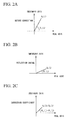
- the modulation signal ⁇ j of the pre-correction subcarrier is represented in a complex plane as shown in FIG. 2A .
- a reflection signal X j (j is an integer from 0 to N-1) of a subcarrier output from the FFT processing unit 113 is represented by Equation (4) below.
- a r (j) is an amplitude of the reflection signal X j of the subcarrier
- ⁇ r (j) is a phase of the reflection signal X j of the subcarrier.
- the reflection signal X j of the subcarrier is represented in the complex plane as shown in FIG. 2B .
- the correction processing unit 114 calculates a correction coefficient c j of each subcarrier from the subcarrier signal X j (j is an integer from 0 to N-1) of the reflection wave output from the FFT processing unit 113 and the modulation signal ⁇ j (j is an integer from 0 to N-1) of each OFDM subcarrier read out from the memory 112 using Equation (5) below, and stores the calculated correction coefficient c j of each subcarrier in the memory 112.
- the amount of correction in an amplitude direction is A s (j)/ A r (j)
- the amount of correction of a phase component is ⁇ s (j)- ⁇ r (j)
- the correction coefficient is represented in the complex plane as shown in FIG. 2C . Both amplitude and phase can be corrected by a correction coefficient.
- the correction processing unit 114 calculates a post-correction signal ⁇ coeff from the calculated correction coefficient c j and the modulation signal ⁇ j of each OFDM subcarrier using Equation (6) below, and outputs the calculated post-correction signal ⁇ coeff to the IFFT processing unit 115.
- the IFFT processing unit 115 performs an inverse FFT (referred to as IFFT below) on the correction signal ⁇ coeff output from the correction processing unit 114, thereby converting the correction signal ⁇ coeff into an OFDM signal in the time domain. Also, the IFFT processing unit 115 inserts a cyclic prefix (CP) between respective OFDM signals as a guide interval, and outputs an in-phase signal I to a digital analog converter (DAC) 121 and a quadrature phase signal Q to a DAC 122.
- CP cyclic prefix
- the transmission circuit 120 includes the DAC 121, the DAC 122, a quadrature modulator 123, a band pass filter 124, a high output power amplifier 125, and a frequency oscillator 127.
- the DAC 121 converts the in-phase signal I output from the IFFT processing unit 115 from a digital signal to an analog signal, and outputs the analog signal to the quadrature modulator 123.
- the DAC 122 converts the quadrature phase signal Q output from the IFFT processing unit 115 from a digital signal to an analog signal, and outputs the analog signal to the quadrature modulator 123.
- the frequency oscillator 127 (includes a phase-locked loop (PLL) not shown) generates a carrier wave of a predetermined band set by the carrier control unit 116, and outputs the generated carrier wave to the quadrature modulator 123.
- the quadrature modulator 123 generates the transmission signal by modulating the analog signal input from the DAC 121 and the analog signal output from the DAC 122 using a cosine wave and a sine wave of the carrier wave output from the frequency oscillator 127, and outputs the transmission signal to the band pass filter 124.
- the band pass filter 124 generates a signal from which unnecessary components are removed by applying the filter to the synthesis signal output from the quadrature modulator 123, and outputs the signal from which the unnecessary components have been removed to the high output power amplifier 125.
- the high output power amplifier 125 amplifies the signal, from which the unnecessary components have been removed and which is input from the band pass filter 124, with a predetermined gain to a power required for outputting, and then outputs the amplified signal to the duplexer 126.
- the reflection wave detection circuit 130 includes a detector 132 (Det), an amplifier 133, and an analog digital converter (ADC) 134.
- the detector 132 (Det) detects a reflection signal that is reflected from the side of the antenna 140 and input through the coupled line 131, and outputs the detected reflection signal to the amplifier 133.
- the amplifier 133 amplifies the reflection signal output from the detector 132 to a level required by the ADC 134, and outputs the amplified reflection signal to the ADC 134.
- the ADC 134 converts the reflection signal (analog signal) output from the amplifier 133 into a digital signal, and outputs the digital signal to the FFT processing unit 113.
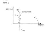
- a degraded fraction and the amount of correction of group delay will be described below using FIG. 3 to FIG. 5 .
- a horizontal axis is frequency
- a vertical axis is group delay.
- the correction processing unit 114 determines to correct the degraded fraction 22 of the group delay of a subcarrier that becomes a correction target, calculates a correction coefficient from Equation (5) above, and multiplies a pre-correction signal of each subcarrier by a correction coefficient of the subcarrier using Equation (6), thereby changing the pre-correction signal of the subcarrier to a post-improvement group delay characteristic 21.
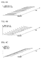
- FIGS. 4A, 4B, and 4C a horizontal axis is frequency, a vertical axis is group delay, and a third axis is time.
- FIG. 4A illustrates a group delay characteristic of a transmission signal, and in FIG. 4A , the transmission signal has the uniform group delay characteristic with respect to all frequencies.
- FIG. 4B illustrates a group delay characteristic of a reflection signal when a filter for suppressing spurious is additionally installed on an antenna. In FIG. 4B , group delay of the reflection signal increases in a low frequency band due to influence of the filter.
- FIG. 4C illustrates the amount of correction of group delay calculated by subtracting the group delay characteristic of the reflection signal from the group delay characteristic of the transmission signal.
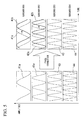
- FIG. 5 a horizontal axis is time, and a vertical axis is amplitude.
- This drawing shows an example in which the correction processing unit 114 performs correction, and thereby phases progress in connection with subcarrier I and subcarrier 2 (subcarrieres that are correction targets) in a low frequency band that may deteriorate, and processing is not performed on subcarrier 3 and subcarrier 4 in a high frequency band.
- the correction processing unit 114 performs correction, so that a phase of a pre-correction signal 41 a of subcarrier 1 progresses, and the pre-correction signal 41a becomes a post-correction signal 41b.
- the correction processing unit 114 performs correction, so that a phase of a pre-correction signal 42a of subcarrier 2 progresses, and the pre-correction signal 42a becomes a post-correction signal 42b.
- changes in phase are not made for signals of subcarrier 3 and subcarrier 4, and the signals remain as a signal 43 and a signal 44 respectively.
- the correction processing unit 114 performs phase correction as illustrated in FIG. 5 by multiplying a pre-correction signal of each subcarrier, which is a correction target, by a correction coefficient of Equation (5). In this manner, it is possible to improve a group delay characteristic.
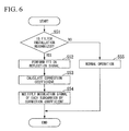
- FIG. 6 is a flowchart of phase correction by the correction processing unit 114.
- the correction processing unit 114 checks whether or not an external filter is installed between the antenna 140 and the coupled line 131.
- a method for the correction processing unit 114 to check installation of a filter will be described below. For example, by manipulation of an operator through an input interface, the correction processing unit 114 may be informed of installation of a filter and recognize installation of a filter. The correction processing unit 114 may recognize installation of a filter from characteristics of a reflection signal based on results obtained by analyzing the reflection signal subjected to FFT processing.
- the correction processing unit 114 may analyze a reflection signal obtained by performing FFT processing on a regularly-transmitted signal (e.g., broadcast channel or downlink shared channel in a communication scheme provided by Third Generation Patnership Project (3GPP)). Also, filter information on characteristics of an installed filter may be stored in advance in the memory 112, and the correction processing unit 114 may determine installation of the filter from the filter information and characteristics of a reflection signal.
- a regularly-transmitted signal e.g., broadcast channel or downlink shared channel in a communication scheme provided by Third Generation Patnership Project (3GPP)
- filter information on characteristics of an installed filter may be stored in advance in the memory 112, and the correction processing unit 114 may determine installation of the filter from the filter information and characteristics of a reflection signal.
- the correction processing unit 114 When the correction processing unit 114 does not recognize that a filter is installed (No in step S51), as a normal operation, the correction processing unit 114 reads out a correction coefficient and a modulation signal calculated on a previous occasion from the memory 112, generates a correction signal by multiplying the modulation signal by the correction coefficient, and outputs the correction signal to the IFFT processing unit 115 (step S55).
- the FFT processing unit 113 When the correction processing unit 114 recognizes that a filter is installed on the side of the antenna 140 (Yes in step S51), the FFT processing unit 113 generates an FFT signal by performing FFT processing on a reflection signal input from the ADC 130, and outputs the FFT signal to the correction processing unit 114 (step S52). Subsequently, the correction processing unit 114 calculates a correction coefficient of each subcarrier from the FFT signal and the modulation signal read out from the memory using Equation (5) above (step S53). Subsequently, the correction processing unit 114 calculates a correction signal by multiplying a modulation signal of each subcarrier by the calculated coefficient, and outputs the correction signal to the IFFT processing unit 115 (step S54). Then, the present processing ends.
- the radio communication device 100 can correct group delay of a transmission signal using a reflection signal, and thereby can improve communication quality even when characteristics of the transmission signal vary after the radio communication device 100 is installed.
- a band pass filter for suppressing spurious installed on an antenna side is installed between a base station and the antenna when the radio communication device 100 is the base station. Also, when the base station is a type installed on a rooftop, the band pass filter may be installed inside a case of the base station.
Landscapes
- Engineering & Computer Science (AREA)
- Computer Networks & Wireless Communication (AREA)
- Signal Processing (AREA)
- Transmitters (AREA)
Abstract
Description
- The present invention relates to a radio communication device.
This application claims priority to and the benefits of Japanese Patent Application No.2010-021381 filed on Feb. 2, 2010 - In Patent Document 1, orthogonal frequency-division multiplexing (referred to as OFDM below) that is one of multi-carrier communication systems is designed to correct deviation caused by a low-pass filter (referred to as LPF below) that suppresses a loop-back signal generated from a digital analog conversion circuit, thereby reducing distortion of an OFDM signal. Specifically, an OFDM signal with low distortion is generated by correcting deviation in advance according to the attenuation characteristic and the group delay characteristic of an LPF circuit. For the method disclosed in Patent Document 1, it is necessary to know characteristics of a filter in advance, but there are cases in which the filter characteristics are not known in advance.
- Patent Document 1 Japanese Unexamined Patent Application, First Publication No.
H06-311134 - For example, when a radio communication device is installed and then a radio wave of a desired signal for transmission interferes to generate spurious, it is further necessary to install an external filter on an antenna. In this case, the newly installed external filter deteriorates deviation of amplitude and phase in a band used for communication, which causes deterioration of communication quality.
- The present invention has been achieved in view of the above circumstances, and it is an object of the present invention to improve communication quality even when characteristics of a desired signal for transmission vary.
- A radio communication device according to an aspect of the present invention includes an amplification unit configured to amplify a transmission signal; an antenna transmitting an amplification signal amplified by the amplification unit; a detection unit configured to detect a reflection signal that is the amplification signal reflected from a side of the antenna; and a correction processing unit configured to correct the transmission signal, wherein the correction processing unit is configured to correct the transmission signal based on the reflection signal when installation of a filter through which the amplification signal passes is recognized.
- In the radio communication device of the aspect of the present invention, the reflection signal may be a signal reflected by the filter.
- The radio communication device of the aspect of the present invention may further include a coupled line configured to receive the reflection signal, and the filter may be disposed between the antenna and the coupled line.
- In the radio communication device of the aspect of the present invention, the correction processing unit may be configured to recognize the installation of the filter when it is informed of manipulation of an operator.
- In the radio communication device of the aspect of the present invention, the correction processing unit may be configured to recognize the installation of the filter based on an analysis result of the reflection signal.
- In the radio communication device of the aspect of the present invention, the transmission signal may be a multicarrier signal including a plurality of subcarrier signals, and the correction processing unit may be configured to correct a phase and an amplitude of a specific subcarrier signal of the multicarrier signal based on the reflection signal.
- In the radio communication device of the aspect of the present invention, the correction processing unit may be configured to correct a phase of a subcarrier signal having delay based on the reflection signal.
- According to the present invention, even when characteristics of a desired signal for transmission vary, it is possible to improve communication quality.
-
-
FIG. 1 is a block configuration diagram of a radio communication device according to an embodiment of the present invention. -
FIG. 2A is a diagram showing a pre-correction signal on a complex plane. -
FIG. 2B is a diagram showing a reflection signal on the complex plane. -
FIG. 2C is a diagram showing a correction coefficient on the complex plane. -
FIG. 3 is a diagram illustrating a degraded fraction and the amount of correction of group delay. -
FIG. 4A is a diagram illustrating a group delay characteristic of a transmission signal. -
FIG. 4B is a diagram illustrating a group delay characteristic of a reflection signal. -
FIG. 4C is a diagram illustrating the amount of correction of group delay calculated by subtracting the group delay characteristic (FIG. 4B ) of the reflection signal from the group delay characteristic (FIG. 4A ) of the transmission signal. -
FIG. 5 is a diagram illustrating correction of phase on a time axis when group delay is in a low-frequency band. -
FIG. 6 is a flowchart of phase correction by acorrection processing unit 114. -
FIG. 7A is a diagram showing an example of a change in amplitude and group delay before and after suppression of spurious in a surrounding band. -
FIG. 7B is a diagram showing another example of a change in amplitude and group delay before and after suppression of spurious in a surrounding band. - Hereinafter, embodiments of the present invention will be described in detail with reference to the drawings.
FIG. 1 is a block configuration diagram of a radio communication device according to an embodiment of the present invention. Aradio communication device 100 includes abaseband unit 110, atransmission circuit 120, a duplexer (Dup) 126, a reflectionwave detection circuit 130, a coupledline 131 and anantenna 140. In the present embodiment, theradio communication device 100 is described as a stationary radio communication device such as a base station. - The
antenna 140 transmits a transmission signal, which is output from thetransmission circuit 120 through theduplexer 126, to another radio terminal (not shown) as a transmission wave. When theantenna 140 transmits the transmission signal, a reflection signal reflected from a side of theantenna 140 is input to theradio communication device 100 through a line that connects theradio communication device 100 with theantenna 140.
The coupledline 131 separates the transmission signal input from thetransmission circuit 120 and the reflection signal reflected from the side of theantenna 140, and outputs the transmission signal to theantenna 140 and the reflection signal to the reflectionwave detection circuit 130.
In the present embodiment, OFDM of a frequency division duplex (FDD) scheme is employed, and thus theduplexer 126 electrically separates a transmission path and a reception path.
Theduplexer 126 separates the transmission signal and a reception signal. Here, description of a reception circuit that processes the reception signal in theradio communication device 100 is omitted. Also, when a time division duplex (TDD) scheme is used, theduplexer 126 switches between transmission and reception by a switch at predetermined time intervals.
After theradio communication device 100 is installed, a band pass filter for suppressing an unnecessary (spurious) wave of a surrounding band of a necessary band of a desired signal may be installed between the coupledline 131 and theantenna 140. - When such a filter is used, deviation of amplitude and phase in a band used for communication deteriorates. As the detailed deterioration, deterioration of amplitude and a group delay characteristic after the spurious of a surrounding band is suppressed will be described using
FIGS. 7A and 7B . In an example shown inFIG. 7A , it can be seen that a band of apost-filter characteristic 72a narrows compared with a pre-filter-processing characteristic 71a. In an example shown inFIG. 7B , it can be seen that group delay of a post-filter characteristic 72b increases in a low-frequency region compared with a pre-filter-processing characteristic 71b. - It has been known that, when spurious is suppressed using a filter in this manner, a group delay characteristic is distorted, and as a result, communication quality of a single-carrier communication system deteriorates. In order to reduce the deterioration in communication quality, a method of avoiding or prohibiting allocation of a deteriorated channel using a multi-carrier communication system has been used. In addition to the method of avoiding or prohibiting allocation of a deteriorated subcarrier, a method of setting a low modulation scheme for a deteriorated subcarrier has been used in OFDM, but there was no preferred method.
- The
baseband unit 110 includes amodulation processing unit 111, amemory 112, anFFT processing unit 113, acorrection processing unit 114, anIFFT processing unit 115 and acarrier control unit 116. - The
modulation processing unit 111 first divides a data string (e.g., a binary data string) into N pieces of parallel data through demultiplexing, modulates each piece of parallel data by quadrature amplitude modulation (referred to as QAM below), phase-shift keying (referred to as PSK below) or the like, and stores the modulated signal (a signal in the frequency domain as a complex number) in thememory 112.
In OFDM, a signal Φ modulated by themodulation processing unit 111 is represented by Equation (1) below. -

- Here, N is the number of carriers, and ϕj (j is an integer from 0 to N-1) is a signal of each subcarrier.
- The
FFT processing unit 113 outputs a reflection signal (complex number) that is output from the reflectionwave detection circuit 130 and subjected to FFT processing using a fast Fourier transform (referred to as FFT below) to the correction processing unit 144.
Specifically, theFFT processing unit 113 performs FFT processing on N reflection signals Xk (k is an integer from 0 to N-1) and thereby calculates N complex sequences (k is an integer from 0 to N-1) from Equation (2) below. -

- Here, e is a Napier's number, i is an imaginary unit, π is the ratio of the circumference of a circle to its diameter, and j is (an integer from 0 to N-1).
- The
correction processing unit 114 corrects each subcarrier of the transmission signal based on the reflection signal output from theFFT processing unit 113. Details are described below. A modulation signal ϕj (j is an integer from 0 to N-1) of each pre-correction subcarrier that is read out from thememory 112 by thecorrection processing unit 114 is represented by Equation (3) below. -

- Here, As(j) is an amplitude of the modulation signal ϕj of the subcarrier, and θs(j) is a phase of the modulation signal ϕj of the subcarrier. The modulation signal ϕj of the pre-correction subcarrier is represented in a complex plane as shown in
FIG. 2A . A reflection signal Xj (j is an integer from 0 to N-1) of a subcarrier output from theFFT processing unit 113 is represented by Equation (4) below. -

- Ar(j) is an amplitude of the reflection signal Xj of the subcarrier, and θr(j) is a phase of the reflection signal Xj of the subcarrier. The reflection signal Xj of the subcarrier is represented in the complex plane as shown in
FIG. 2B . - The
correction processing unit 114 calculates a correction coefficient cj of each subcarrier from the subcarrier signal Xj (j is an integer from 0 to N-1) of the reflection wave output from theFFT processing unit 113 and the modulation signal ϕj (j is an integer from 0 to N-1) of each OFDM subcarrier read out from thememory 112 using Equation (5) below, and stores the calculated correction coefficient cj of each subcarrier in thememory 112. -

- Here, the amount of correction in an amplitude direction is As(j)/ Ar(j), the amount of correction of a phase component is θs(j)-θr(j), and the correction coefficient is represented in the complex plane as shown in
FIG. 2C . Both amplitude and phase can be corrected by a correction coefficient.
Thecorrection processing unit 114 calculates a post-correction signal Φcoeff from the calculated correction coefficient cj and the modulation signal ϕj of each OFDM subcarrier using Equation (6) below, and outputs the calculated post-correction signal Φcoeff to theIFFT processing unit 115. -

- The
IFFT processing unit 115 performs an inverse FFT (referred to as IFFT below) on the correction signal Φcoeff output from thecorrection processing unit 114, thereby converting the correction signal Φcoeff into an OFDM signal in the time domain.
Also, theIFFT processing unit 115 inserts a cyclic prefix (CP) between respective OFDM signals as a guide interval, and outputs an in-phase signal I to a digital analog converter (DAC) 121 and a quadrature phase signal Q to aDAC 122. - The
transmission circuit 120 includes theDAC 121, theDAC 122, aquadrature modulator 123, aband pass filter 124, a highoutput power amplifier 125, and afrequency oscillator 127. - The
DAC 121 converts the in-phase signal I output from theIFFT processing unit 115 from a digital signal to an analog signal, and outputs the analog signal to thequadrature modulator 123.
TheDAC 122 converts the quadrature phase signal Q output from theIFFT processing unit 115 from a digital signal to an analog signal, and outputs the analog signal to thequadrature modulator 123. - The frequency oscillator 127 (includes a phase-locked loop (PLL) not shown) generates a carrier wave of a predetermined band set by the
carrier control unit 116, and outputs the generated carrier wave to thequadrature modulator 123.
Thequadrature modulator 123 generates the transmission signal by modulating the analog signal input from theDAC 121 and the analog signal output from theDAC 122 using a cosine wave and a sine wave of the carrier wave output from thefrequency oscillator 127, and outputs the transmission signal to theband pass filter 124. - The
band pass filter 124 generates a signal from which unnecessary components are removed by applying the filter to the synthesis signal output from thequadrature modulator 123, and outputs the signal from which the unnecessary components have been removed to the highoutput power amplifier 125.
The highoutput power amplifier 125 amplifies the signal, from which the unnecessary components have been removed and which is input from theband pass filter 124, with a predetermined gain to a power required for outputting, and then outputs the amplified signal to theduplexer 126. - The reflection
wave detection circuit 130 includes a detector 132 (Det), anamplifier 133, and an analog digital converter (ADC) 134.
The detector 132 (Det) detects a reflection signal that is reflected from the side of theantenna 140 and input through the coupledline 131, and outputs the detected reflection signal to theamplifier 133.
Theamplifier 133 amplifies the reflection signal output from thedetector 132 to a level required by theADC 134, and outputs the amplified reflection signal to theADC 134.
TheADC 134 converts the reflection signal (analog signal) output from theamplifier 133 into a digital signal, and outputs the digital signal to theFFT processing unit 113. - Details of processing of the
correction processing unit 114 will be described below usingFIG. 3 to FIG. 5 . First, usingFIG. 3 , a degraded fraction and the amount of correction of group delay will be described. In this drawing, a horizontal axis is frequency, and a vertical axis is group delay.
When a filter that cuts a low frequency region is newly installed between the coupledline 131 and theantenna 140 in order to suppress close spurious, group delay of the filter increases in a low frequency region. In this manner, a peak of group delay (adegraded fraction 22 of the group delay) as shown inFIG. 3 is observed.
Thecorrection processing unit 114 determines to correct thedegraded fraction 22 of the group delay of a subcarrier that becomes a correction target, calculates a correction coefficient from Equation (5) above, and multiplies a pre-correction signal of each subcarrier by a correction coefficient of the subcarrier using Equation (6), thereby changing the pre-correction signal of the subcarrier to a post-improvement group delay characteristic 21. - Next, correction described in
FIG. 3 will be described usingFIGS. 4A, 4B, and 4C . InFIGS. 4A, 4B, and 4C , a horizontal axis is frequency, a vertical axis is group delay, and a third axis is time.FIG. 4A illustrates a group delay characteristic of a transmission signal, and inFIG. 4A , the transmission signal has the uniform group delay characteristic with respect to all frequencies.FIG. 4B illustrates a group delay characteristic of a reflection signal when a filter for suppressing spurious is additionally installed on an antenna. InFIG. 4B , group delay of the reflection signal increases in a low frequency band due to influence of the filter.FIG. 4C illustrates the amount of correction of group delay calculated by subtracting the group delay characteristic of the reflection signal from the group delay characteristic of the transmission signal. - Next, correction described in
FIG. 3 will be described usingFIG. 5 . InFIG. 5 , a horizontal axis is time, and a vertical axis is amplitude. This drawing shows an example in which thecorrection processing unit 114 performs correction, and thereby phases progress in connection with subcarrier I and subcarrier 2 (subcarrieres that are correction targets) in a low frequency band that may deteriorate, and processing is not performed on subcarrier 3 and subcarrier 4 in a high frequency band. Specifically, thecorrection processing unit 114 performs correction, so that a phase of apre-correction signal 41 a of subcarrier 1 progresses, and thepre-correction signal 41a becomes apost-correction signal 41b. Likewise, thecorrection processing unit 114 performs correction, so that a phase of apre-correction signal 42a of subcarrier 2 progresses, and thepre-correction signal 42a becomes apost-correction signal 42b. In addition, changes in phase are not made for signals of subcarrier 3 and subcarrier 4, and the signals remain as asignal 43 and asignal 44 respectively.
As described above, thecorrection processing unit 114 performs phase correction as illustrated inFIG. 5 by multiplying a pre-correction signal of each subcarrier, which is a correction target, by a correction coefficient of Equation (5). In this manner, it is possible to improve a group delay characteristic. - Processing flow of phase correction by the
correction processing unit 114 will be described.FIG. 6 is a flowchart of phase correction by thecorrection processing unit 114.
First, thecorrection processing unit 114 checks whether or not an external filter is installed between theantenna 140 and the coupledline 131.
A method for thecorrection processing unit 114 to check installation of a filter will be described below.
For example, by manipulation of an operator through an input interface, thecorrection processing unit 114 may be informed of installation of a filter and recognize installation of a filter.
Thecorrection processing unit 114 may recognize installation of a filter from characteristics of a reflection signal based on results obtained by analyzing the reflection signal subjected to FFT processing. At this time, thecorrection processing unit 114 may analyze a reflection signal obtained by performing FFT processing on a regularly-transmitted signal (e.g., broadcast channel or downlink shared channel in a communication scheme provided by Third Generation Patnership Project (3GPP)). Also, filter information on characteristics of an installed filter may be stored in advance in thememory 112, and thecorrection processing unit 114 may determine installation of the filter from the filter information and characteristics of a reflection signal.
When thecorrection processing unit 114 does not recognize that a filter is installed (No in step S51), as a normal operation, thecorrection processing unit 114 reads out a correction coefficient and a modulation signal calculated on a previous occasion from thememory 112, generates a correction signal by multiplying the modulation signal by the correction coefficient, and outputs the correction signal to the IFFT processing unit 115 (step S55). - When the
correction processing unit 114 recognizes that a filter is installed on the side of the antenna 140 (Yes in step S51), theFFT processing unit 113 generates an FFT signal by performing FFT processing on a reflection signal input from theADC 130, and outputs the FFT signal to the correction processing unit 114 (step S52). Subsequently, thecorrection processing unit 114 calculates a correction coefficient of each subcarrier from the FFT signal and the modulation signal read out from the memory using Equation (5) above (step S53). Subsequently, thecorrection processing unit 114 calculates a correction signal by multiplying a modulation signal of each subcarrier by the calculated coefficient, and outputs the correction signal to the IFFT processing unit 115 (step S54). Then, the present processing ends. - As described above, the
radio communication device 100 can correct group delay of a transmission signal using a reflection signal, and thereby can improve communication quality even when characteristics of the transmission signal vary after theradio communication device 100 is installed. - Although embodiments of the present invention have thus far been described in detail with reference to the drawings, the detailed configuration is not limited to these embodiments but includes design and the like within a scope that does not depart from the spirit of the present invention. A band pass filter for suppressing spurious installed on an antenna side is installed between a base station and the antenna when the
radio communication device 100 is the base station. Also, when the base station is a type installed on a rooftop, the band pass filter may be installed inside a case of the base station. - According to the present invention, even when an unnecessary wave of a surrounding band of a necessary band is suppressed and characteristics of a desired signal for transmission vary, it is possible to improve communication quality.
-
- 100
- radio communication device
- 110
- baseband unit
- 111
- modulation processing unit
- 112
- memory
- 113
- FFT processing unit
- 114
- correction processing unit
- 115
- IFFT processing unit
- 116
- carrier control unit
- 120
- transmission circuit
- 121
- DAC
- 122
- DAC
- 123
- quadrature modulator
- 124
- band pass filter
- 125
- high output power amplifier
- 126
- duplexer
- 127
- frequency oscillator
- 130
- reflection wave detection circuit
- 131
- coupled line
- 132
- detector
- 133
- amplifier
- 134
- ADC
- 140
- antenna
Claims (7)
- A radio communication device comprising:an amplification unit configured to amplify a transmission signal;an antenna transmitting an amplification signal amplified by the amplification unit;a detection unit configured to detect a reflection signal that is the amplification signal reflected from a side of the antenna; anda correction processing unit configured to correct the transmission signal,wherein the correction processing unit is configured to correct the transmission signal based on the reflection signal when installation of a filter through which the amplification signal passes is recognized.
- The radio communication device according to claim 1, wherein the reflection signal is a signal reflected by the filter.
- The radio communication device according to claim 2, further comprising a coupled line receiving the reflection signal,
wherein the filter is disposed between the antenna and the coupled line. - The radio communication device according to claim 1, wherein the correction processing unit is configured to recognize the installation of the filter when it is informed of manipulation of an operator.
- The radio communication device according to claim 1, wherein the correction processing unit is configured to recognize the installation of the filter based on an analysis result of the reflection signal.
- The radio communication device according to claim 2, wherein the transmission signal is a multicarrier signal including a plurality of subcarrier signals, and
the correction processing unit is configured to correct a phase and an amplitude of a specific subcarrier signal of the multicarrier signal based on the reflection signal. - The radio communication device according to claim 6, wherein the correction processing unit is configured to correct a phase of a subcarrier signal having delay based on the reflection signal.
Applications Claiming Priority (2)
| Application Number | Priority Date | Filing Date | Title |
|---|---|---|---|
| JP2010021381 | 2010-02-02 | ||
| PCT/JP2011/052132 WO2011096427A1 (en) | 2010-02-02 | 2011-02-02 | Wireless communication apparatus |
Publications (2)
| Publication Number | Publication Date |
|---|---|
| EP2533442A1 true EP2533442A1 (en) | 2012-12-12 |
| EP2533442A4 EP2533442A4 (en) | 2016-06-01 |
Family
ID=44355423
Family Applications (1)
| Application Number | Title | Priority Date | Filing Date |
|---|---|---|---|
| EP11739775.2A Withdrawn EP2533442A4 (en) | 2010-02-02 | 2011-02-02 | WIRELESS COMMUNICATION APPARATUS |
Country Status (6)
| Country | Link |
|---|---|
| US (1) | US8798179B2 (en) |
| EP (1) | EP2533442A4 (en) |
| JP (1) | JP5456068B2 (en) |
| KR (1) | KR20120115402A (en) |
| CN (1) | CN102742196A (en) |
| WO (1) | WO2011096427A1 (en) |
Cited By (1)
| Publication number | Priority date | Publication date | Assignee | Title |
|---|---|---|---|---|
| FR3002345A1 (en) * | 2013-02-15 | 2014-08-22 | St Microelectronics Sa | METHOD AND DEVICE FOR TRANSMITTING A RADIO FREQUENCY SIGNAL |
Families Citing this family (6)
| Publication number | Priority date | Publication date | Assignee | Title |
|---|---|---|---|---|
| JP5752005B2 (en) * | 2010-12-17 | 2015-07-22 | 京セラ株式会社 | Transmitter |
| JP2013046077A (en) * | 2011-08-22 | 2013-03-04 | Kyocera Corp | Radio communication system |
| WO2014061444A1 (en) * | 2012-10-17 | 2014-04-24 | 株式会社村田製作所 | Transceiver device |
| JP6275423B2 (en) * | 2013-09-06 | 2018-02-07 | 株式会社Nttドコモ | Wireless base station, wireless communication system, and wireless communication method |
| WO2015151745A1 (en) * | 2014-03-31 | 2015-10-08 | 株式会社村田製作所 | Transmission/reception apparatus and reflected signal suppression method |
| CN110411334B (en) * | 2019-07-01 | 2021-04-06 | 上海工程技术大学 | Improved phase carrier PGC demodulation method and system |
Family Cites Families (18)
| Publication number | Priority date | Publication date | Assignee | Title |
|---|---|---|---|---|
| US4011512A (en) * | 1975-05-21 | 1977-03-08 | Motorola, Inc. | Electrical component failure detection apparatus |
| JP2781946B2 (en) * | 1993-04-27 | 1998-07-30 | シャープ株式会社 | Orthogonal frequency division multiplex signal generator |
| CN1166138C (en) * | 2000-07-20 | 2004-09-08 | 华为技术有限公司 | Adaptive digital pre-distortion method and device for wideband transmitter |
| CN1254925C (en) * | 2001-09-27 | 2006-05-03 | 株式会社东芝 | Portable radio apparatus |
| EP1514379A2 (en) * | 2002-05-31 | 2005-03-16 | Koninklijke Philips Electronics N.V. | Message routing in a radio network |
| TWI220817B (en) * | 2003-08-22 | 2004-09-01 | Benq Corp | Antenna matching device and method thereof |
| DE102004047724A1 (en) * | 2003-09-30 | 2005-05-25 | Infineon Technologies Ag | Transmission device for transceiver, has complex multiplication unit to logically combines predistortion coefficient with baseband signals, and power amplifier to compensate for amplitude modulation/phase modulation distortion |
| US20080008109A1 (en) * | 2004-09-21 | 2008-01-10 | Jeffrey Ollis | Method and apparatus for bridging wireless control networks |
| KR100678946B1 (en) * | 2004-11-26 | 2007-02-07 | 삼성전자주식회사 | Method and apparatus for sharing channels in coordinator-based wireless network |
| EP1819038A4 (en) * | 2004-11-30 | 2008-07-09 | Fujitsu Ltd | SIGNAL EXTRACTION CIRCUIT AND DISTORTION AMPLIFIER THEREFOR |
| JP4619230B2 (en) | 2004-12-15 | 2011-01-26 | 株式会社日立国際電気 | Distortion compensation amplifier |
| GB0503291D0 (en) * | 2005-02-17 | 2005-03-23 | Eleksen Ltd | Mobile communication |
| DE102005015713B4 (en) | 2005-04-06 | 2009-01-08 | Tuchenhagen Dairy Systems Gmbh | Method and device for degassing and maintaining a continuous volume flow of a milk to be treated in an ultra-high-temperature (UHT) system |
| JP2006340166A (en) * | 2005-06-03 | 2006-12-14 | Nippon Dengyo Kosaku Co Ltd | Distortion compensation amplifier |
| JP4792273B2 (en) * | 2005-10-18 | 2011-10-12 | 株式会社日立国際電気 | amplifier |
| EP2033325A2 (en) * | 2006-04-26 | 2009-03-11 | Qualcomm Incorporated | Duty cycling power scheme |
| US7843834B2 (en) * | 2006-09-15 | 2010-11-30 | Itron, Inc. | Use of minimal propagation delay path to optimize a mesh network |
| US8351874B2 (en) * | 2008-04-08 | 2013-01-08 | Telefonaktiebolaget Lm Ericsson (Publ) | System and method for adaptive antenna impedance matching |
-
2011
- 2011-02-02 KR KR1020127021216A patent/KR20120115402A/en not_active Ceased
- 2011-02-02 US US13/576,140 patent/US8798179B2/en not_active Expired - Fee Related
- 2011-02-02 EP EP11739775.2A patent/EP2533442A4/en not_active Withdrawn
- 2011-02-02 WO PCT/JP2011/052132 patent/WO2011096427A1/en not_active Ceased
- 2011-02-02 JP JP2011552795A patent/JP5456068B2/en not_active Expired - Fee Related
- 2011-02-02 CN CN201180007714XA patent/CN102742196A/en active Pending
Non-Patent Citations (1)
| Title |
|---|
| See references of WO2011096427A1 * |
Cited By (2)
| Publication number | Priority date | Publication date | Assignee | Title |
|---|---|---|---|---|
| FR3002345A1 (en) * | 2013-02-15 | 2014-08-22 | St Microelectronics Sa | METHOD AND DEVICE FOR TRANSMITTING A RADIO FREQUENCY SIGNAL |
| US9270300B2 (en) | 2013-02-15 | 2016-02-23 | Stmicroelectronics Sa | Radio frequency signal transmission method and device |
Also Published As
| Publication number | Publication date |
|---|---|
| US20120314807A1 (en) | 2012-12-13 |
| JP5456068B2 (en) | 2014-03-26 |
| WO2011096427A1 (en) | 2011-08-11 |
| JPWO2011096427A1 (en) | 2013-06-10 |
| KR20120115402A (en) | 2012-10-17 |
| EP2533442A4 (en) | 2016-06-01 |
| US8798179B2 (en) | 2014-08-05 |
| CN102742196A (en) | 2012-10-17 |
Similar Documents
| Publication | Publication Date | Title |
|---|---|---|
| US8798179B2 (en) | Radio communication device | |
| US20140355718A1 (en) | Device for modifying trajectories | |
| US20170118060A1 (en) | Blind Carrier Synchronization Method of OFDM Wireless Communication Systems | |
| US9130623B2 (en) | User equipment and method for radio communication system | |
| US9967126B2 (en) | Method to generate a wireless waveform for use in a wireless communication system, a wireless communication system and computer program products thereof | |
| US12244334B2 (en) | Selecting a modulation scheme to mitigate specific fault types in 5G and 6G | |
| US20020181610A1 (en) | Multicarrier transmission apparatus and multicarrier transmission method | |
| EP3439255B1 (en) | A method to provide increased robustness against noise and interference in wireless communications, a transmitter and computer program products thereof | |
| US9838735B2 (en) | Prevention of erroneous detection of signal | |
| US20160128010A1 (en) | Single carrier frequency domain equalizer time synchronization in a broadband transceiver | |
| US20100232530A1 (en) | Communication apparatus | |
| US20050052990A1 (en) | Orthogonal frequency division multiplexing error vector magnitude calibration based on separate multi-tone measurement | |
| WO2016039668A2 (en) | Interference mitigation | |
| US7894540B2 (en) | Method and apparatus for reducing phase noise in orthogonal frequency division multiplexing systems | |
| JPH11289312A (en) | Multi-carrier wireless communication device | |
| US8861641B2 (en) | Wireless communication device and wireless communication method | |
| EP1724956A1 (en) | Radio system and radio communication device | |
| US8363750B2 (en) | Apparatus, method and computer program for error compensation | |
| US8780942B2 (en) | Communication device and a delay amount detection method | |
| JP4998207B2 (en) | Communication apparatus and method for compensating for in-phase quadrature mismatch | |
| EP2706714A1 (en) | Signal processing device and method of processing at least two input signals for a transmitter of a communications device | |
| US20140254503A1 (en) | Signal detector for uplink control channel and time error correction method thereof | |
| KR20130104837A (en) | Operating method of transmitter in a wireless comunication | |
| KR20110041283A (en) | Signal receiving device and method in wireless communication system and system for same |
Legal Events
| Date | Code | Title | Description |
|---|---|---|---|
| PUAI | Public reference made under article 153(3) epc to a published international application that has entered the european phase |
Free format text: ORIGINAL CODE: 0009012 |
|
| 17P | Request for examination filed |
Effective date: 20120731 |
|
| AK | Designated contracting states |
Kind code of ref document: A1 Designated state(s): AL AT BE BG CH CY CZ DE DK EE ES FI FR GB GR HR HU IE IS IT LI LT LU LV MC MK MT NL NO PL PT RO RS SE SI SK SM TR |
|
| DAX | Request for extension of the european patent (deleted) | ||
| RA4 | Supplementary search report drawn up and despatched (corrected) |
Effective date: 20160503 |
|
| RIC1 | Information provided on ipc code assigned before grant |
Ipc: H04B 1/04 20060101ALI20160426BHEP Ipc: H04J 11/00 20060101AFI20160426BHEP |
|
| STAA | Information on the status of an ep patent application or granted ep patent |
Free format text: STATUS: THE APPLICATION HAS BEEN WITHDRAWN |
|
| 18W | Application withdrawn |
Effective date: 20171103 |